WO2022249233A1 - ソフトエラー検出装置とその方法 - Google Patents
ソフトエラー検出装置とその方法 Download PDFInfo
- Publication number
- WO2022249233A1 WO2022249233A1 PCT/JP2021/019580 JP2021019580W WO2022249233A1 WO 2022249233 A1 WO2022249233 A1 WO 2022249233A1 JP 2021019580 W JP2021019580 W JP 2021019580W WO 2022249233 A1 WO2022249233 A1 WO 2022249233A1
- Authority
- WO
- WIPO (PCT)
- Prior art keywords
- soft error
- memory unit
- unit
- memory
- error detection
- Prior art date
- Legal status (The legal status is an assumption and is not a legal conclusion. Google has not performed a legal analysis and makes no representation as to the accuracy of the status listed.)
- Ceased
Links
Images




Classifications
-
- G—PHYSICS
- G06—COMPUTING OR CALCULATING; COUNTING
- G06F—ELECTRIC DIGITAL DATA PROCESSING
- G06F11/00—Error detection; Error correction; Monitoring
- G06F11/07—Responding to the occurrence of a fault, e.g. fault tolerance
- G06F11/16—Error detection or correction of the data by redundancy in hardware
-
- G—PHYSICS
- G11—INFORMATION STORAGE
- G11C—STATIC STORES
- G11C29/00—Checking stores for correct operation ; Subsequent repair; Testing stores during standby or offline operation
- G11C29/52—Protection of memory contents; Detection of errors in memory contents
Definitions
- the present invention relates to a soft error detection device and method for detecting soft errors that occur in electronic equipment due to incident particle radiation.
- Particle radiation has the properties of particles, such as proton beams, alpha rays, and neutron beams.
- particles such as proton beams, alpha rays, and neutron beams.
- neutrons are produced when cosmic rays from outer space collide with oxygen and nitrogen in the atmosphere.
- a semiconductor device for example, memory
- a "soft error” may have a serious impact on social infrastructure in some cases.
- Non-Patent Document 1 a technology to identify the particle radiation energy that caused soft errors using FPGA (Field Programmable Gate Array) and measure the rate of soft errors generated for each particle radiation energy is disclosed, for example, in Non-Patent Document 1.
- FPGA Field Programmable Gate Array
- Non-Patent Document 1 detects soft errors by rewriting data in the lookup table (equivalent to the above memory) for determining the circuit configuration of the FPGA. However, it uses only one bit of the register that specifies the range of the lookup table. In other words, only part of the lookup table of the FPGA can be used.
- the conventional technology has the problem that the memory area (semiconductor device) where soft errors are detected is not fully utilized.
- the present invention has been made in view of this problem, and it is an object of the present invention to provide a soft error detection device and method that can effectively utilize the memory area where soft errors are detected.
- a soft error detection device is a soft error detection device that detects a soft error caused by incidence of particle radiation, comprising: a frequency divider that divides a clock signal input from the outside; a code length selection unit for selecting a code length of a binary code representing the operating state of the device, a first memory unit storing predetermined data, and a second memory unit storing data different from the first memory unit , a first multiplexer for selecting data from either one of said first memory unit and said second memory unit based on the selected binary code; and a third memory storing the same data as said first memory unit. a fourth memory unit storing the same data as the second memory unit; and selecting data from either the third memory unit or the fourth memory unit based on the selected binary code.
- a second multiplexer compares a first output signal output by the first multiplexer and a second output signal output by the second multiplexer in synchronization with the clock signal, and detects the soft error when they do not match. and a soft error detection unit.
- a soft error detection method is a soft error detection method performed by the above soft error detection device, wherein the frequency divider divides the frequency of the clock signal input from the outside, and the code length A selection unit selects a code length of a binary code representing an operation state of the frequency dividing unit, and a first multiplexer selects a first memory unit storing predetermined data based on the selected binary code, and the Select one of the data in the second memory section storing data different from the data in the first memory section, and the second multiplexer stores the same data as in the first memory section based on the selected binary code.
- the gist of the invention is to compare the output signal and a second output signal output by the second multiplexer, and to detect the soft error when they do not match.
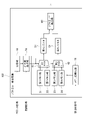
- FIG. 1 is a block diagram showing a functional configuration example of a soft error detection device according to a first embodiment of the present invention
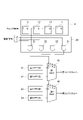
- FIG. 2 is a configuration diagram showing a specific example of a frequency dividing section and a code length selecting section shown in FIG. 1
- FIG. 2 is a configuration diagram showing a specific example of a first multiplexer shown in FIG. 1
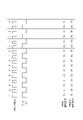
- FIG. 2 is a time chart showing an operation example of a frequency divider and first and second registers shown in FIG. 1
- 4 is a time chart showing another operation example of the frequency divider and the first and second registers shown in FIG. 1
- It is a figure which shows the relationship example of neutron energy and flight time.
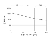
- FIG. 2 is a flow chart showing a processing procedure of a soft error detection method performed by the soft error detection device shown in FIG. 1; It is a figure which shows the relationship example of the time-of-flight of a neutron, and a logical failure occurrence probability. It is a figure which shows the relationship example of neutron energy and flight time.
- FIG. 1 is a block diagram showing a functional configuration example of a soft error detection device according to the first embodiment of the present invention.
- the soft error detection device 100 shown in FIG. 1 detects soft errors caused by incident particle radiation.
- Particle radiation refers to beta rays, proton rays, and neutron rays that have the properties of particles (electrons, protons, neutrons) among radiation.
- particle radiation enters a semiconductor device, it may cause the soft error described above.
- the soft error detection device 100 includes a frequency dividing section 10, a code length selecting section 20, a first memory section 31, a second memory section 32, a first multiplexer 41, a third memory section 33, a fourth memory section 34, and a second multiplexer. 42 , a first register 51 , a second register 52 , a soft error detection section 60 and a memory initialization section 70 .
- the frequency dividing unit 10 is a frequency dividing circuit that divides the input clock signal, and can be composed of flip-flops.
- the frequency dividing unit 10 having four T-type flip-flops connected in cascade outputs frequencies obtained by dividing the frequency of the clock signal into 1/2, 1/4, 1/8 and 1/16.
- the code length selection unit 20 selects the code length of the binary code representing the operating state of the frequency division unit 10 .
- the code length selection unit 20 outputs the selected binary code whose code length is selected.
- the operating state of the frequency divider 10 is the state of each flip-flop in the process of dividing the clock signal.
- the frequency divider 10 which is formed by connecting four T-type flip-flops in cascade, has 16 operating states from 0 to F represented by hexadecimal numbers. Details of the frequency divider 10 and the code length selector 20 will be described later.
- the first memory unit 31 stores predetermined data.
- the first memory unit 31 is composed of, for example, a RAM and is set to all "0". The greater the amount of data in the first memory unit 31, the higher the "soft error" detection efficiency.
- the amount of data in the first memory unit 31 will be explained with an example of 8 bits, for example.
- the amount of data can be set to an arbitrary size by arranging a large number of first memory units 31 in the depth direction of the drawing.
- the first memory unit 31 can be set to an arbitrary data amount by arranging the same configuration in parallel.
- the second memory section 32 stores data different from that of the first memory section 31 . All "0"s in the first memory unit 31 are set to “1"s. Other points are the same as the first memory unit 31 .
- the first multiplexer 41 selects either the first memory unit 31 or the second memory unit 32 based on the selected binary code representing the operation state of the frequency dividing unit 10 selected by the code length selecting unit 20. or select data.
- the first MUX 41 selects the data of the first memory section 31 .
- the first MUX 41 selects the data of the second memory unit 32 .
- the first MUX 41 alternately selects data in the first memory section 31 and the second memory section 32 each time the state of the selected binary code changes.
- data "0" in the first memory section 31 and data "1" in the second memory section 32 are alternately selected corresponding to the state of the selected binary code.
- the third memory section 33 stores the same data as the first memory section 31.
- the third memory section 33 is configured similarly to the first memory section 31 .
- the fourth memory section 34 stores the same data as the second memory section 32 .
- the fourth memory section 34 is configured similarly to the second memory section 32 .
- the second multiplexer 42 (hereinafter referred to as the second MUX 42) selects either the third memory unit 43 or the fourth memory unit 34 based on the selected binary code representing the operation state of the frequency dividing unit 10 selected by the code length selecting unit 20. or select data.
- the second MUX 42 selects the data of the third memory section 43.
- FIG. Also, when the output of the code length selection unit 20 is “1”, the second MUX 42 selects the data of the fourth memory unit 44 .
- the first memory section 31 and the third memory section 33, the second memory section 32 and the fourth memory section 34, and the first MUX 41 and the second MUX 42 are the same. Therefore, when no soft error occurs (when each of the first memory unit 31 to the fourth memory unit 34 does not change due to neutrons), each of the first MUX 41 and the second MUX 42 selects the same data.
- the first register 51 holds the selection signal (first output signal) of the first MUX 41 in synchronization with the above clock signal.
- the clock signal of the first register 51 is the same as the clock signal input to the frequency divider 10, and is omitted from FIG.
- the second register 52 holds the selection signal (second output signal) of the second MUX 42 in synchronization with the above clock signal. As with the first register 51, the notation of the clock signal of the second register 52 is omitted.
- the soft error detection unit 60 compares the first output signal output by the first MUX 41 in synchronization with the clock signal and the second output signal output by the second MUX 42, and detects a "soft error” if they do not match.
- the soft error detection unit 60 is composed of, for example, an exclusive OR (EXOR gate).
- each of the first memory section 31 to the fourth memory section 34 is assumed to be 8 bits. Also, each of the first and second MUXes 41 and 42, the first and second registers 51 and 52, and the soft error detection section 60 will be explained using one example.
- FIG. 2 is a configuration diagram showing a specific example of the frequency divider 10 and the code length selector 20 according to this embodiment.
- the first and second MUXs 41 and 42 and the first and second registers 51 and 52 shown in FIG. 2 are the same as those in FIG. 1 as is clear from the reference numerals.
- the frequency divider 10 has a configuration in which, for example, four T-type flip-flops (hereinafter referred to as T-type FFs) are connected in series.
- a clock signal is input to the T terminal of the T-type FF11 in the first stage, and the Q output of the T-type FF11 is input to the T terminal of the T-type FF12 in the next stage.
- the Q output of the T-type FF 12 is input to the T terminal of the T-type FF 13 in the third stage, and the Q output of the T-type FF 13 is input to the T terminal of the T-type FF 14 in the fourth stage.
- the frequency divider 10 is configured by connecting four T-type FFs 11 to 14 in cascade.
- the code length selection unit 20 is composed of, for example, four logical products (AND gates) enabled by each of the 4-bit control signals S1 to S4.
- the Q output of the T-type FF 11 is connected to the other terminal of the logical product 21, one terminal of which is connected to the control signal S1.
- the logical product 22 to which the Q output of the T-type FF 12 is connected is enabled by the control signal S2.
- a logical product 23 to which the Q output of the T-type FF 13 is connected is enabled by the control signal S3.
- a logical product 24 to which the Q output of the T-type FF 14 is connected is enabled by the control signal S4.
- the code length selection unit 20 outputs the selected binary code whose code length is selected based on the control signals S1 to S4.
- FIG. 3 is a configuration diagram showing a specific example of the first MUX 41.
- the first MUX 41 is composed of 15 MUXes (reference numerals omitted) controlled by the selected binary code output from the code length selection section 20. 2 Select each bit of the memory section 32 . Each of the four selected binary codes is connected to input terminals ⁇ to ⁇ of the first MUX 41 .
- the input terminals ⁇ to ⁇ of the first MUX 41 are inputs to a 4-input 1-output address selection circuit.
- the first MUX 41 selects one bit from each bit of the first memory section 31 and the second memory section 32 corresponding to the state of the selected binary code (input terminals ⁇ to ⁇ ).
- the states represented by 4 bits of input terminals ⁇ to ⁇ are represented by 16 states 0 to F(15).
- the first MUX 41 selects the first bit 311 of the first memory section 31 .
- the operation of the first MUX 41 described above is the same for the second MUX 42 as well.
- the second MUX 42 is different in that one bit is selected from each bit of the third memory section 33 and the fourth memory section 34 .
- FIG. 4 is a time chart showing the selected binary code output by the code length selection unit 20, the selection signal of the first MUX 41, and the selection signal of the second MUX 42, respectively.
- the horizontal direction in FIG. 4 represents the passage of time, and the vertical direction represents the state of each signal.
- FIG. 4 shows selected binary codes (input terminals ⁇ to ⁇ ) when the control signals S1 to S4 are all "1".
- each Q output of the T-type FFs 11-14 of the frequency divider 10 changes at the rising edge of the clock signal
- each Q output of the T-type FFs 11-14 is 0, 0, 0, 0 (0) at the rising edge of the clock signal. to 1,1,1,1 (F).
- the Q outputs of the T-type FFs 11 to 14 are E, D, C, B, A, 9, 8, 7, 6, 5, 4, 3, 2, 1, 1, 2, 3 in synchronization with the rising edge of the clock signal It changes in the order of 0.
- This F to 0 matches the selected binary code (input terminals ⁇ to ⁇ ).
- the first MUX 41 selects the eighth bit 328 of the second memory section 32 . Also, the second MUX 42 in this case selects the eighth bit 348 of the fourth memory unit 34 .
- the first MUX 41 selects the eighth bit 318 of the first memory section 31 . Also, the second MUX 42 in this case selects the eighth bit 338 of the third memory unit 33 .
- the first MUX 41 selects one of the data of the first memory section 31 and the second memory section 32 set to the same data
- the second MUX 42 selects the data of the third memory section 33 set to the same data.
- One of the data in the fourth memory section 34 is selected.
- the first register 51 (Fig. 1) holds the signal selected by the first MUX 41 in synchronization with the clock signal. Also, the second register 52 similarly holds the signal selected by the first MUX 42 .
- the soft error detection unit 60 compares the signals held by the first register 51 and the second register 52 (output signals of each register), and detects a soft error when they do not match. If no soft error occurs, the signals held in the first register 51 and the second register 52 always match. Therefore, the output of the soft error detector (EXOR gate) 60 is always "0".
- the soft error detection unit 60 When the Q outputs of the T-type FFs 11 to 14 are 8, for example, and the signals held in the first register 51 and the second register 52 do not match, the soft error detection unit 60 immediately detects a soft error (EXOR gate). The output changes to "1" (not shown). When a soft error is detected, a control section (not shown) generates an initialization signal, and a memory initialization section 70 initializes the first memory section 31 to the fourth memory section 34 to predetermined data.
- a soft error EXOR gate
- the data for initializing the first memory unit 31 to the fourth memory unit 34 are, for example, all “0” or all “1” above. Data to be compared are not limited to all "0” or all “1". The process of soft error detection and initialization of the memory section may be repeated.
- the memory initialization unit 70 may be omitted.
- a controller (not shown) controls the memory initialization unit 70 .
- a control unit will be described in a second embodiment.
- the code length of the selected binary code is 4 bits in this way, it is possible to detect soft errors by comparing all the corresponding bits in the first memory unit 31 to the fourth memory unit 34 .
- the comparison can be performed in 16 periods of the clock signal.
- the code length of the selected binary code is 1 bit, only the input signal ⁇ is valid, and a soft error is detected by comparing some corresponding bits in the first memory unit 31 to the fourth memory unit 34. do.
- FIG. 5 is a time chart showing each of the selected binary code, the selection signal of the first MUX 41, and the selection signal of the second MUX 42 when the code length of the selected binary code is 1 bit.
- the first MUX 41 alternately selects the 5th bit 31-5 and the 1st bit 31-1 of the first memory section 31 .
- the second MUX 42 alternately selects the fifth bit 33-5 and the first bit 33-1 of the third memory section 33 .
- the corresponding 2 bits in the first memory unit 31 to the fourth memory unit 34 are compared to detect a soft error.
- soft errors can be detected with a resolution of 10 ns (5 ns ⁇ 2).
- Table 1 shows the relationship between the code length of the selected binary code, detection resolution, and detection efficiency.
- the detection efficiency is the ratio of the size of the memory areas of the first memory unit 31 to the fourth memory unit 34 used for soft error detection. It is a ratio based on the case where it is fixed to 1”.
- the detection resolution is the time interval for detecting soft errors. By reducing the size of the memory areas of the first memory unit 31 to the fourth memory unit 34 used for soft error detection, it is possible to reduce the detection resolution and detect soft errors. It should be noted that if the detection resolution is reduced, the detection efficiency will deteriorate.
- the soft error detection resolution and detection efficiency can be varied by changing the code length of the selected binary code.
- the energy of particle radiation is proportional to its flight speed. Therefore, by setting the code length (selected binary code) corresponding to the energy region of the particle radiation to be measured, it is possible to efficiently measure the soft error.
- FIG. 6 is a diagram showing an example of the relationship between neutron energy and flight time.
- the horizontal axis of FIG. 6 is the neutron energy [MeV], and the vertical axis is the neutral flight speed.
- soft errors caused by fast neutrons can be detected in a short time
- soft errors caused by slow neutrons can be detected in a long time without exception.
- the soft error detection device 100 is a soft error detection device that detects soft errors caused by incidence of particle radiation.
- a code length selection unit 20 for selecting a code length of a binary code representing the operating state of the frequency dividing unit 10, a first memory unit 31 storing predetermined data, and data different from the first memory unit 31.
- the second memory unit 32 stored, the first MUX 41 that selects data in either the first memory unit 31 or the second memory unit 32 based on the selected binary code, and the same as the first memory unit 31
- a third memory unit 33 storing data, a fourth memory unit 34 storing the same data as the second memory unit 32, and a third memory unit 33 and a fourth memory unit based on the selected binary code.
- Effective use of memory areas means reducing unused memory areas (or eliminating unused areas). According to this embodiment, by setting the code length of the selected binary code to 4 bits, all the bits of the first to fourth memory units 31 to 34 can be used to detect soft errors.
- each functional component of the first memory unit 31, the second memory unit 32, the third memory unit 33, the fourth memory unit 34, the first MUX 41, and the second MUX 42 is a combinational logic circuit of FPGA (combination logic circuit). information) can be replaced with a lookup table (truth table).
- the first memory unit 31, the second memory unit 32, the third memory unit 33, the fourth memory unit 34, the first MUX 41, and the second MUX 42 may be configured with FGPA lookup tables.
- a configuration including other functional configuration units (the frequency dividing unit 10, etc.) and a sequential circuit can also be realized by FPGA. As a result, development costs can be reduced.
- the code length selection unit 20 selects the code length of the binary code representing the operating state of the frequency division unit 10 based on the control signals S1 to S4 input from the outside. Thereby, the detection resolution and detection efficiency of the soft error detection device 100 can be varied from the outside.
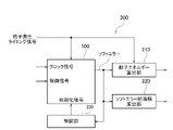
- FIG. 7 is a block diagram showing a functional configuration example of a soft error detection device according to the second embodiment of the present invention.
- a soft error detection device 200 shown in FIG. 7 is obtained by adding a particle energy calculation unit 210, a soft error cross-sectional area calculation unit 220, and a control unit 230 to the soft error detection device 100 (FIG. 1).
- the particle energy calculation unit 210 calculates the particle energy of particle radiation based on the difference between the time when the particle radiation was generated and the detection time when the soft error was detected.
- the generation time of particle radiation is obtained from the particle generation timing signal input from the outside.
- the particle generation timing signal is a signal representing the time when a target that generates particle radiation is irradiated with, for example, protons.
- the particle energy calculation unit 210 starts measuring an internal timer (not shown) upon input of the particle generation timing signal. After that, when the output of the soft error detection unit 60 (soft error detection device 100) changes (“0” ⁇ “1”), the timer is stopped to measure the flight time of the particle radiation.
- the soft error detection device 100 is placed in an environment where particle radiation is applied.
- Other functional components of the soft error detection device 200 are placed in an environment where particle radiation is not applied.
- An environment that is not irradiated with particle radiation is, for example, a space surrounded by shielding walls.
- the particle energy calculator 210 that has measured the time of flight of the particle radiation calculates the particle energy E n by the time of flight method (equation (1)).
- m0 is the mass of the particle radiation
- c is the speed of light
- L is the distance between the target and the soft error detection device 100
- t is the above difference.
- the soft error cross-sectional area calculation unit 220 calculates the soft error cross-sectional area by dividing the number of detected soft errors by the number of particle radiation incident on a unit area.
- the number of detected soft errors is obtained by repeatedly changing the output of the soft error detection unit 60 for a predetermined period of time.
- the control unit 230 operates the memory initialization unit 70 to initialize the data in the first memory unit 31 to the fourth memory unit 34 and repeat the operation of soft error detection for a predetermined time.
- the soft error detection device 100 is operated as follows. The number of iterations is the number of detected soft errors.
- the number of particle radiation incident on a unit area may be measured by measuring the number of environments in which the particle radiation is irradiated, or may be stored in advance as a constant in the soft error cross-sectional area calculation unit 220. good.
- the soft error cross section represents the probability of occurrence of soft errors caused by one particle radiation per unit area.
- the soft error cross section is used to calculate the failure rate of semiconductor devices due to soft errors.
- the soft error detection device 200 may include either one of the particle energy calculator 210 and the soft error cross-sectional area calculator 220, or both.
- the soft error detection device 200 includes a particle energy calculator 210 that calculates the particle energy of particle radiation based on the difference between the particle radiation generation time and the detection time when the soft error is detected. Thereby, the particle energy of the particle radiation can be calculated.
- the soft error detection device 200 also includes a soft error cross-sectional area calculator 220 that calculates a soft error cross-sectional area by dividing the number of detected soft errors by the number of particle radiation incident on a unit area. Thereby, the soft error cross-sectional area can be calculated.
- FIG. 8 is a flowchart showing a processing procedure of a soft error detection method performed by the soft error detection device 100. As shown in FIG.
- the frequency divider 10 divides the frequency of the clock signal (step S1).
- the code length selection unit 20 outputs a selected binary code having a selected code length of the binary code representing the operating state of the frequency division unit 10 (step S2).
- the first MUX 41 selects data in either the first memory section 31 or the second memory section 32 based on the selected binary code.
- the first register 51 then holds the output signal of the second MUX 42 in synchronization with the clock signal (step S3).
- the second MUX 42 selects data in either the third memory section 33 or the fourth memory section 34 based on the selected binary code. Then, the second register 52 holds the output signal of the first MUX 41 in synchronization with the clock signal (step S4).
- the soft error detection unit 60 synchronizes with the clock signal, compares the first output signal output by the first MUX 41 and the second output signal output by the second MUX 42, and detects a soft error when they do not match (step S5).
- the processing of steps S1 to S4 is repeated until a soft error is detected (NO in step S5).
- the soft error detection method is a soft error detection method performed by the soft error detection device 100 that detects soft errors caused by incidence of particle radiation.
- the code length selection unit 20 selects the code length of the binary code representing the operating state of the frequency division unit 10, and the first MUX 41 selects the binary code based on the selected binary code. Either the first memory section 31 storing predetermined data or the second memory section 32 storing data different from the first memory section 31 is selected, and the second MUX 42 converts the selected binary Data is selected from one of the third memory section 33 storing the same data as the first memory section 31 and the fourth memory section 34 storing the same data as the second memory section 32 based on the code, and clocked.
- the first output signal output by the first MUX 41 and the second output signal output by the second MUX 42 are compared, and if they do not match, a soft error is detected. Accordingly, it is possible to provide a soft error detection method capable of effectively utilizing a memory area in which soft errors are detected.
- FIG. 9 is a diagram showing an example of the relationship between the time of flight of neutrons (particle radiation) and the probability of logical failure occurrence.
- the horizontal axis of FIG. 9 is the time of flight [ns], and the vertical axis is the logical fault occurrence probability.
- neutrons with short flight times cause many logical disturbances. Since flight time and neutron (particle radiation) energy are proportional (Fig. 6), high-energy neutrons cause many logical disturbances (soft errors).
- the detection resolution can be set according to the magnitude of the energy of the particle radiation. That is, the detection resolution is set small for neutrons with high energy. Also, the detection resolution is set large for neutrons with small energy. This makes it possible to reduce the statistical error of soft errors.
- FIG. 10 is a diagram showing an example of the relationship between neutron energy and soft error cross section.
- the horizontal axis of FIG. 10 is the neutron energy [Mev], and the vertical axis is the soft error cross section.
- the characteristics shown in Fig. 10 have large variations in the soft error cross section for neutron energies of 3 Mev or less. According to the soft error detection devices 100 and 200, the variation can be reduced by setting a large detection resolution for neutrons in this energy band.
- the soft error detection devices 100 and 200 can reduce the statistical error and shorten the measurement time.
- the data amount of the first memory unit 31 to the fourth memory unit 34 is 8 bits. can be easily increased to the order of
- the frequency divider 10 has been described with an example in which four T-type FFs are cascaded, the present invention is not limited to this example. It is possible to configure an arbitrary number of stages corresponding to the amount of data in the memory.
Landscapes
- Engineering & Computer Science (AREA)
- Theoretical Computer Science (AREA)
- Quality & Reliability (AREA)
- Physics & Mathematics (AREA)
- General Engineering & Computer Science (AREA)
- General Physics & Mathematics (AREA)
- Measurement Of Radiation (AREA)
Abstract
外部から入力されるクロック信号を分周する分周部10と、分周部10の動作状態を表す二進符号の符号長を選択する符号長選択部20と、所定のデータが格納された第1メモリ部31と、第1メモリ部31と異なるデータが格納された第2メモリ部32と、選択された二進符号に基づいて第1メモリ部31と第2メモリ部32のどちらか一方のデータを選択する第1MUX41と、第1メモリ部31と同じデータが格納された第3メモリ部33と、第2メモリ部32と同じデータが格納された第4メモリ部34と、選択された二進符号に基づいて第3メモリ部33と第4メモリ部34のどちらか一方のデータを選択する第2MUX42と、クロック信号に同期させて第1MUX41が出力する第1出力信号と、クロック信号に同期させて第2MUX42が出力する第2出力信号を比較し、不一致の場合にソフトエラーを検出するソフトエラー検出部60とを備える。
Description
本発明は、粒子放射線の入射によって電子機器に生じるソフトエラーを検出するソフトエラー検出装置とその方法に関する。
粒子放射線は、放射線の中でも陽子線、アルファ線、中性子線のように粒子の性質を持つものである。例えば中性子は、宇宙から降り注ぐ宇宙線が大気圏中の酸素や窒素に衝突することで発生する。この中性子が、電子機器の半導体デバイス(例えばメモリ)に衝突すると、保存されていたデータが書き変わる「ソフトエラー」を引き起こす。「ソフトエラー」は、場合によっては社会インフラに重大な影響を及ぼす可能性がある。
上記のソフトエラーを検出するために、FPGA(Field Programmable Gate Array)を用いてソフトエラーを引き起こした粒子放射線のエネルギーを特定し、その粒子放射線のエネルギー毎にソフトエラーを発生させる割合を計測する技術が、例えば非特許文献1に開示されている。
Hidenori Iwashita , Gentaro Funatsu, Hirotaka Sato, Takashi Kamiyama, Michihiro Furusaka, Stephen A. Wender, Eric Pitcher, and Yoshiaki Kiyanagi,"Energy-Resolved Soft-Error Rate Measurements for 1-800 MeV Neutrons by the Time-of-Flight Technique at LANSCE",IEEE TRANSACTIONS ON NUCLEAR SCIENCE, VOL. 67, NO. 11, NOVEMBER 2020
非特許文献1に開示された技術は、ソフトエラーをFPGAの回路構成を決定するためのルックアップテーブル(上記のメモリに相当)のデータの書き変わりで検出するものである。しかし、ルックアップテーブルの範囲を指定するレジスタを1ビットしか使用していない。つまり、FPGAのルックアップテーブルの一部分しか使用できていない。
このように従来の技術は、ソフトエラーが検知されるメモリ領域(半導体デバイス)を十分に生かしていないという課題がある。
本発明は、この課題に鑑みてなされたものであり、ソフトエラーが検知されるメモリ領域を有効に活用できるソフトエラー検出装置とその方法を提供することを目的とする。
本発明の一態様に係るソフトエラー検出装置は、粒子放射線の入射によって生じるソフトエラーを検出するソフトエラー検出装置において、外部から入力されるクロック信号を分周する分周部と、前記分周部の動作状態を表す二進符号の符号長を選択する符号長選択部と、所定のデータが格納された第1メモリ部と、前記第1メモリ部と異なるデータが格納された第2メモリ部と、選択された二進符号に基づいて前記第1メモリ部と前記第2メモリ部のどちらか一方のデータを選択する第1マルチプレクサと、前記第1メモリ部と同じデータが格納された第3メモリ部と、前記第2メモリ部と同じデータが格納された第4メモリ部と、選択された二進符号に基づいて前記第3メモリ部と前記第4メモリ部のどちらか一方のデータを選択する第2マルチプレクサと、前記クロック信号に同期させて、前記第1マルチプレクサが出力する第1出力信号と前記第2マルチプレクサが出力する第2出力信号を比較し、不一致の場合に前記ソフトエラーを検出するソフトエラー検出部とを備えることを要旨とする。
また、本発明の一態様に係るソフトエラー検出方法は、上記のソフトエラー検出装置が行うソフトエラー検出方法であって、分周部は、外部から入力されるクロック信号を分周し、符号長選択部は、前記分周部の動作状態を表す二進符号の符号長を選択し、第1マルチプレクサは、選択された二進符号に基づいて所定のデータが格納された第1メモリ部と前記第1メモリ部と異なるデータが格納定された第2メモリ部のどちらか一方のデータを選択し、第2マルチプレクサは、選択された二進符号に基づいて前記第1メモリ部と同じデータが格納された第3メモリ部と前記第2メモリ部と同じデータが格納された第4メモリ部のどちらか一方のデータを選択し、前記クロック信号に同期させて、前記第1マルチプレクサが出力する第1出力信号と前記第2マルチプレクサが出力する第2出力信号を比較し、不一致の場合に前記ソフトエラーを検出することを要旨とする。
本発明によれば、ソフトエラーが検知されるメモリ領域を有効に活用できるソフトエラー検出装置とその方法を提供することができる。
以下、本発明の実施形態について図面を用いて説明する。複数の図面中同一のものには同じ参照符号を付し、説明は繰り返さない。
〔第1実施形態〕
図1は、本発明の第1実施形態に係るソフトエラー検出装置の機能構成例を示すブロック図である。図1に示すソフトエラー検出装置100は、粒子放射線の入射によって生じるソフトエラーを検出するものである。
図1は、本発明の第1実施形態に係るソフトエラー検出装置の機能構成例を示すブロック図である。図1に示すソフトエラー検出装置100は、粒子放射線の入射によって生じるソフトエラーを検出するものである。
粒子放射線とは、放射線の中でも粒子(電子、陽子、中性子)の性質を持つベータ線、陽子線、及び中性子線等のことである。粒子放射線が半導体デバイスに入射すると、上記のソフトエラーを生じさせる場合がある。
ソフトエラー検出装置100は、分周部10、符号長選択部20、第1メモリ部31、第2メモリ部32、第1マルチプレクサ41、第3メモリ部33、第4メモリ部34、第2マルチプレクサ42、第1レジスタ51、第2レジスタ52、ソフトエラー検出部60、及びメモリ初期化部70を備える。
分周部10は、入力されるクロック信号を分周する分周回路であり、フリップフロップで構成できる。例えば、4つのT型フリップフロップを縦続接続させた分周部10は、クロック信号の周波数を1/2、1/4、1/8、1/16に分周したそれぞれの周波数を出力する。
符号長選択部20は、分周部10の動作状態を表す二進符号の符号長を選択する。符号長選択部20は、符号長が選択された選択二進符号を出力する。分周部10の動作状態とは、クロック信号を分周する過程の各フリップフロップの状態である。4つのT型フリップフロップを縦続接続させた分周部10は、16進数で表される0~Fの16の動作状態を持つ。分周部10と符号長選択部20について詳しくは後述する。
第1メモリ部31は、所定のデータを格納する。第1メモリ部31は、例えばRAMで構成され全て「0」に設定される。第1メモリ部31のデータ量は、多い程、「ソフトエラー」の検出効率を高めることができる。
つまり、半導体デバイス内における第1メモリ部31の面積が大きい程、中性子が衝突し易くなる。よって、第1メモリ部31のデータ量は多い程好ましい。
ここでは説明の都合により、第1メモリ部31のデータ量は、例えば8ビットの例で説明する。なお、図1において、図面の奥行き方向に第1メモリ部31を多数配置することでデータ量は任意の大きさに設定することが可能である。
例えば、図1の奥行き方向に第1メモリ部31を32個重ねて構成した場合(図示せず)、そのデータ量は32×8=256ビットである。このように、第1メモリ部31は、同じ構成を並列に配置することで任意のデータ量に設定することができる。
第2メモリ部32は、第1メモリ部31と異なるデータが格納される。第1メモリ部31の全て「0」に対して、全て「1」に設定される。その他の点は、第1メモリ部31と同じである。
第1マルチプレクサ41(以降、第1MUX41)は、符号長選択部20で選択された分周部10の動作状態を表す選択二進符号に基づいて第1メモリ部31と第2メモリ部32のどちらか一方のデータを選択する。符号長選択部20の出力が「0」の場合、第1MUX41は第1メモリ部31のデータを選択する。また、符号長選択部20の出力が「1」の場合、第1MUX41は第2メモリ部32のデータを選択する。
したがって、第1MUX41は、選択二進符号の状態が変化する度に、第1メモリ部31と第2メモリ部32のデータを交互に選択する。この例の場合は、選択二進符号の状態に対応させて第1メモリ部31のデータ「0」と、第2メモリ部32のデータ「1」を交互に選択する。
第3メモリ部33は、第1メモリ部31と同じデータが格納される。第3メモリ部33は、第1メモリ部31と同様に構成される。
第4メモリ部34は、第2メモリ部32と同じデータが格納される。第4メモリ部34は、第2メモリ部32と同様に構成される。
第2マルチプレクサ42(以降、第2MUX42)は、符号長選択部20で選択された分周部10の動作状態を表す選択二進符号に基づいて第3メモリ部43と第4メモリ部34のどちらか一方のデータを選択する。符号長選択部20の出力が「0」の場合、第2MUX42は第3メモリ部43のデータを選択する。また、符号長選択部20の出力が「1」の場合、第2MUX42は第4メモリ部44のデータを選択する。
このように、第1メモリ部31と第3メモリ部33、第2メモリ部32と第4メモリ部34、及び第1MUX41と第2MUX42のそれぞれは同じものである。したがって、ソフトエラーが生じない場合(第1メモリ部31~第4メモリ部34のそれぞれが中性子によって変化しない場合)においては、第1MUX41と第2MUX42のそれぞれは同じデータを選択する。
第1レジスタ51は、上記のクロック信号に同期させて第1MUX41の選択信号(第1出力信号)を保持する。第1レジスタ51のクロック信号は、分周部10に入力されるクロック信号と同じであり、図1ではその表記を省略している。
第2レジスタ52は、上記のクロック信号に同期させて第2MUX42の選択信号(第2出力信号)を保持する。第1レジスタ51と同様に第2レジスタ52のクロック信号の表記は省略している。
ソフトエラー検出部60は、クロック信号に同期させて第1MUX41が出力する第1出力信号と、第2MUX42が出力する第2出力信号を比較し、不一致の場合に「ソフトエラー」を検出する。ソフトエラー検出部60は、例えば排他的論理和(EXORゲート)で構成される。
例えば、図1の奥行き方向に第1メモリ部31を32個重ねて構成した場合、第1MUX41、第2MUX42、第1レジスタ51、第2レジスタ52、及びソフトエラー検出部60のそれぞれも32個重ねて構成される。
以降の説明において、第1メモリ部31~第4メモリ部34のそれぞれのデータ量は8ビットとする。また、第1・第2MUX41,42、第1・第2レジスタ51,52、及びソフトエラー検出部60のそれぞれは1個の例で説明する。
(分周部と符号長選択部)
図2は、本実施形態に係る分周部10と符号長選択部20の具体例を示す構成図である。図2に示す第1・第2MUX41,42、第1・第2レジスタ51,52は、参照符号から明らかなように図1と同じものである。
図2は、本実施形態に係る分周部10と符号長選択部20の具体例を示す構成図である。図2に示す第1・第2MUX41,42、第1・第2レジスタ51,52は、参照符号から明らかなように図1と同じものである。
分周部10は、例えば4つのT型フリップフロップ(以降、T型FF)が直列に接続された構成である。初段のT型FF11のT端子にクロック信号が入力され、T型FF11のQ出力が次段のT型FF12のT端子に入力される。T型FF12のQ出力が3段目のT型FF13のT端子に入力され、T型FF13のQ出力が4段目のT型FF14のT端子に入力される。このように分周部10は、4個のT型FF11~14が縦続接続されて構成される。
符号長選択部20は、例えば4ビットの制御信号S1~S4のそれぞれによって有効になる4つの論理積(ANDゲート)で構成される。制御信号S1が一方の端子に接続される論理積21の他方の端子はT型FF11のQ出力が接続される。
T型FF12のQ出力が接続される論理積22は制御信号S2で有効になる。T型FF13のQ出力が接続される論理積23は制御信号S3で有効になる。T型FF14のQ出力が接続される論理積24は制御信号S4で有効になる。
このように、符号長選択部20は、制御信号S1~S4に基づいて符号長が選択された選択二進符号を出力する。
図3は、第1MUX41の具体例を示す構成図である。第1MUX41は、符号長選択部20が出力する選択二進符号で制御される15個のMUX(参照符号省略)で構成され、選択二進符号の状態に対応させて第1メモリ部31と第2メモリ部32の各ビットを選択する。4つの選択二進符号のそれぞれは、第1MUX41の入力端子α~Δに接続される。
第1MUX41の入力端子α~Δは、4入力1出力のアドレス選択回路の入力である。第1MUX41は、選択二進符号(入力端子α~Δ)の状態に対応させて第1メモリ部31と第2メモリ部32の各ビットの中から一つのビットを選択する。
ここで、入力端子α~Δの4ビットで表される状態を0~F(15)の16状態で表現する。入力端子α~Δの状態が0(α=0,β=0,γ0,Δ=0)の場合、第1MUX41は第1メモリ部31の1ビット目311を選択する。入力端子α~Δの状態が1(α=0,β=0,γ0,Δ=1)の場合は第2メモリ部32の1ビット目321を選択する。
同様に、入力端子α~Δの状態が2(α=0,β=0,γ1,Δ=0)で第1メモリ部31の2ビット目312、その状態が3(α=0,β=0,γ1,Δ=1)で第2メモリ部32の2ビット目322がそれぞれ選択される。途中省略、状態が14(α=1,β=1,γ1,Δ=0)で第1メモリ部31の8ビット目318、状態が15(α=1,β=1,γ1,Δ=1)で第2メモリ部32の8ビット目328が選択される。
以上説明した第1MUX41の動作は、第2MUX42についても同様である。ただし、第2MUX42は、第3メモリ部33と第4メモリ部34の各ビットの中から一つのビットを選択する点で異なる。
図4は、符号長選択部20が出力する選択二進符号、第1MUX41の選択信号、及び第2MUX42の選択信号のそれぞれを示すタイムチャートである。図4の横方向は時間経過を表し、縦方向は各信号の状態を表す。図4は、制御信号S1~S4が全て「1」の場合の選択二進符号(入力端子α~Δ)を示す。
分周部10のT型FF11~14は、クロック信号の立ち上がりエッジで変化すると仮定すると、クロック信号の立ち上がりエッジで、T型FF11~14の各Q出力は0,0,0,0(0)から1,1,1,1(F)に変化する。その後、T型FF11~14のQ出力は、クロック信号の立ち上がりエッジに同期して、E,D,C,B,A,9,8,7,6,5,4,3,2,1,0の順に変化する。このF~0は、選択二進符号(入力端子α~Δ)に一致している。
選択二進符号がFの場合、第1MUX41は第2メモリ部32の8ビット目328を選択する。また、この場合の第2MUX42は第4メモリ部34の8ビット目348を選択する。
選択二進符号がEの場合、第1MUX41は第1メモリ部31の8ビット目318を選択する。また、この場合の第2MUX42は第3メモリ部33の8ビット目338を選択する。
このように第1MUX41は、同じデータに設定された第1メモリ部31と第2メモリ部32のデータの一方を選択する、又、第2MUX42は、同じデータに設定された第3メモリ部33と第4メモリ部34のデータの一方を選択する。
第1レジスタ51(図1)は、クロック信号に同期させて第1MUX41で選択された信号を保持する。また、第2レジスタ52は、同様に第1MUX42で選択された信号を保持する。
ソフトエラー検出部60は、第1レジスタ51と第2レジスタ52がそれぞれ保持した信号(各レジスタの出力信号)を比較し、不一致の場合にソフトエラーを検出する。ソフトエラーが生じていない場合は、第1レジスタ51と第2レジスタ52でそれぞれ保持した信号は必ず一致する。よって、ソフトエラー検出部(EXORゲート)60の出力は常に「0」である。
第1メモリ部31~第4メモリ部34の何処かのビットが中性子によって変化すると、第1レジスタ51と第2レジスタ52でそれぞれ保持した信号の一方が変化する。その結果、第1レジスタ51と第2レジスタ52がそれぞれ保持する信号は不一致となり、ソフトエラー検出部60はソフトエラーを検出する。
T型FF11~14のQ出力が例えば8の状態において、第1レジスタ51と第2レジスタ52でそれぞれ保持した信号が不一致になると、ソフトエラー検出部60は直ちにソフトエラーを検出(EXORゲート)の出力が「1」に変化する(図示せず)。ソフトエラーが検出されると、制御部(図示せず)が初期化信号を生成し、メモリ初期化部70は第1メモリ部31~第4メモリ部34を所定のデータに初期化する。
第1メモリ部31~第4メモリ部34を初期化するデータは、例えば上記の全て「0」又は全て「1」である。なお、比較するデータは全て「0」又は全て「1」に限られない。このソフトエラー検出とメモリ部の初期化の処理は、繰り返し行ってもよい。
ソフトエラー検出を繰り返し行わない場合、メモリ初期化部70は無くても構わない。メモリ初期化部70の制御は制御部(図示せず)が行う。制御部については第2実施形態で説明する。
このように選択二進符号の符号長を4ビットとすると、第1メモリ部31~第4メモリ部34の対応する全てのビットを比較してソフトエラーを検出することができる。その比較は、クロック信号の16周期で行うことができる。
クロック信号の周波数を200Mhzと仮定した場合、80ns(5ns×16)の分解能でソフトエラーを検出することができる。
また、選択二進符号の符号長を1ビットとすると、入力信号Δのみが有効であり、第1メモリ部31~第4メモリ部34の対応する一部のビットを比較してソフトエラーを検出する。
図5は、選択二進符号の符号長を1ビットとした場合の選択二進符号、第1MUX41の選択信号、及び第2MUX42の選択信号のそれぞれを示すタイムチャートである。
図5に示すように、選択二進符号の符号長を1ビットにした場合、第1MUX41は第1メモリ部31の5ビット目315と1ビット目311を交互に選択する。また、第2MUX42は第3メモリ部33の5ビット目335と1ビット目331を交互に選択する。
このように選択二進符号の符号を1ビットとすると、第1メモリ部31~第4メモリ部34の対応する2ビットを比較してソフトエラーを検出する。この場合、検出する対象のメモリ領域は狭くなるが10ns(5ns×2)の分解能でソフトエラーを検出することができる。
表1に、選択二進符号の符号長、検出分解能、及び検出効率の関係を示す。

ここで検出効率は、ソフトエラーの検出に使用する第1メモリ部31~第4メモリ部34のメモリ領域の大きさの比率であり、検出効率=1は選択二進符号を「0」又は「1」に固定した場合を基準とする比率である。
検出分解能は、ソフトエラーを検出する時間間隔である。ソフトエラー検出に使用する第1メモリ部31~第4メモリ部34のメモリ領域の大きさを小さくすると検出分解能を小さくしてソフトエラーを検出することができる。なお、検出分解能を小さくすると検出効率は悪くなる。
表1に示すように、選択二進符号の符号長を変えることでソフトエラーの検出分解能と検出効率を可変することができる。
粒子放射線のエネルギーは、その飛行速度に比例する。よって、計測対象の粒子放射線のエネルギー領域に対応させた符号長(選択二進符号)にすることで、ソフトエラーを効率的に計測することが可能である。
図6は、中性子エネルギーと飛行時間の関係例を示す図である。図6の横軸は中性子エネルギー[MeV]、縦軸は中性性の飛行速度である。
図6に示すように、中性子エネルギーが小さいと飛行時間は長く、そのエネルギーが大きいと飛行時間は短くなる。したがって、計測対象の中性子エネルギーに対応させて符号長を変えることで、ソフトエラーを効率的に計測することができる。
つまり、高速な中性子によるソフトエラーは短い時間で検出でき、低速な中性子によるソフトエラーは長い時間で漏れなく検出することができる。
以上説明したように、本実施形態に係るソフトエラー検出装置100は、粒子放射線の入射によって生じるソフトエラーを検出するソフトエラー検出装置において、外部から入力されるクロック信号を分周する分周部10と、分周部10の動作状態を表す二進符号の符号長を選択する符号長選択部20と、所定のデータが格納された第1メモリ部31と、第1メモリ部31と異なるデータが格納された第2メモリ部32と、選択された二進符号に基づいて第1メモリ部31と第2メモリ部32のどちらか一方のデータを選択する第1MUX41と、第1メモリ部31と同じデータが格納された第3メモリ部33と、第2メモリ部32と同じデータが格納された第4メモリ部34と、選択された二進符号に基づいて第3メモリ部33と第4メモリ部34のどちらか一方のデータを選択する第2MUX42と、クロック信号に同期させて、第1MUX41が出力する第1出力信号と第2MUX42が出力する第2出力信号を比較し、不一致の場合にソフトエラーを検出するソフトエラー検出部60とを備える。これにより、ソフトエラーが検知されるメモリ領域を有効に活用できるソフトエラー検出装置を提供することができる。
メモリ領域を有効に活用とは、未使用のメモリ領域を小さくする(又は未使用の領域を無くす)ことを意味する。本実施形態によれば、選択二進符号の符号長を4ビットにすることで第1メモリ部31~第4メモリ部34の全てのビットを使用してソフトエラーを検出することができる。
なお、上記の第1メモリ部31、第2メモリ部32、第3メモリ部33、第4メモリ部34、第1MUX41、及び第2MUX42の各機能構成部は、FPGAの組み合わせ論理(組合せロジックの回路情報)を実現するルックアップテーブル(真理値表)に置き替えることが可能である。
つまり、第1メモリ部31、第2メモリ部32、第3メモリ部33、第4メモリ部34、第1MUX41、及び第2MUX42は、FGPAのルックアップテーブルで構成してもよい。その場合、他の機能構成部(分周部10等)及び順序回路を含む構成もFPGAで実現することができる。これにより、開発費を安価にすることができる。
また、符号長選択部20は、外部から入力される制御信号S1~S4に基づいて分周部10の動作状態を表す二進符号の符号長を選択する。これにより、外部からソフトエラー検出装置100の検出分解能と検出効率を可変することができる。
〔第2実施形態〕
図7は、本発明の第2実施形態に係るソフトエラー検出装置の機能構成例を示すブロック図である。図7に示すソフトエラー検出装置200は、ソフトエラー検出装置100(図1)に、粒子エネルギー算出部210、ソフトエラー断面積算出部220、及び制御部230を付加したものである。
図7は、本発明の第2実施形態に係るソフトエラー検出装置の機能構成例を示すブロック図である。図7に示すソフトエラー検出装置200は、ソフトエラー検出装置100(図1)に、粒子エネルギー算出部210、ソフトエラー断面積算出部220、及び制御部230を付加したものである。
粒子エネルギー算出部210は、粒子放射線の発生時刻とソフトエラーを検出した検出時刻の差分に基づいて粒子放射線の粒子エネルギーを算出する。
粒子放射線の発生時刻は、外部から入力される粒子発生タイミング信号で得られる。粒子発生タイミング信号は、粒子放射線を生成するターゲットに例えば陽子を照射した時刻を表す信号である。
粒子エネルギー算出部210は、粒子発生タイミング信号の入力で内部のタイマー(図示せず)の計測を開始させる。その後、ソフトエラー検出部60(ソフトエラー検出装置100)の出力が変化(「0」→「1」)したらタイマーの計測を停止させて粒子放射線の飛行時間を計測する。
なお、ソフトエラー検出装置100は、粒子放射線が照射される環境に配置される。それ以外のソフトエラー検出装置200の機能構成部(粒子エネルギー算出部210等)は、粒子放射線が照射されない環境に配置される。粒子放射線が照射されない環境は、例えば遮蔽壁で囲まれた空間である。
粒子放射線の飛行時間を計測した粒子エネルギー算出部210は、飛行時間法(式(1))により粒子エネルギーEnを算出する。

ここでm0は粒子放射線の質量、cは光速、Lはターゲットとソフトエラー検出装置100との間の距離、tは上記の差分である。
ソフトエラー断面積算出部220は、ソフトエラーの検出数を、単位面積に入射する粒子放射線の数で除してソフトエラー断面積を算出する。
ソフトエラーの検出数は、ソフトエラー検出部60の出力の変化を、所定時間の間繰り返して求める。制御部230は、ソフトエラーが検出されると、メモリ初期化部70を作用させて第1メモリ部31~第4メモリ部34のデータの初期化→ソフトエラー検出の動作を所定時間の間繰り返すようにソフトエラー検出装置100を動作させる。この繰り返しの回数がソフトエラーの検出数になる。
単位面積に入射する粒子放射線の数は、粒子放射線が照射される環境のその数を測定器で測定してもよいし、予め定数としてソフトエラー断面積算出部220内に記憶させるようにしてもよい。
ソフトエラー断面積は、1つの粒子放射線が単位面積当たりに引き起こすソフトエラーの発生確率を表す。ソフトエラー断面積は、ソフトエラーによる半導体デバイスの故障率を計算するのに用いる。
ソフトエラー検出装置200は、粒子エネルギー算出部210とソフトエラー断面積算出部220のどちらか一方、又は両方を備えてもよい。
つまり、ソフトエラー検出装置200は、粒子放射線の発生時刻とソフトエラーを検出した検出時刻の差分に基づいて粒子放射線の粒子エネルギーを算出する粒子エネルギー算出部210を備える。これにより、粒子放射線の粒子エネルギーを算出することができる。
また、ソフトエラー検出装置200は、ソフトエラーの検出数を、単位面積に入射す粒子放射線の数で除してソフトエラー断面積を算出するソフトエラー断面積算出部220を備える。これにより、ソフトエラー断面積を算出することができる。
(ソフトエラー検出方法)
図8は、ソフトエラー検出装置100が行うソフトエラー検出方法の処理手順を示すフローチャートである。
図8は、ソフトエラー検出装置100が行うソフトエラー検出方法の処理手順を示すフローチャートである。
ソフトエラー検出装置100が動作を開始すると分周部10は、クロック信号を分周する(ステップS1)。
次に、符号長選択部20は、分周部10の動作状態を表す二進符号の符号長を選択した選択二進符号を出力する(ステップS2)。
次に、第1MUX41は、選択二進符号に基づいて第1メモリ部31と第2メモリ部32のどちらか一方のデータを選択する。そして、第1レジスタ51は、クロック信号に同期させて第2MUX42の出力信号を保持する(ステップS3)。
また、第2MUX42は、選択二進符号に基づいて第3メモリ部33と第4メモリ部34のどちらか一方のデータを選択する。そして、第2レジスタ52は、クロック信号に同期させて第1MUX41の出力信号を保持する(ステップS4)。
そして、ソフトエラー検出部60は、クロック信号に同期させて、第1MUX41が出力する第1出力信号と第2MUX42が出力する第2出力信号を比較し、不一致の場合にソフトエラーを検出する(ステップS5)。ステップS1~S4の処理はソフトエラーが検出されるまで繰り返される(ステップS5のNO)。
以上説明したように、本実施形態に係るソフトエラー検出方法は、粒子放射線の入射によって生じるソフトエラーを検出するソフトエラー検出装置100が行うソフトエラー検出方法であって、分周部10は、外部から入力されるクロック信号を分周し、符号長選択部20は、分周部10の動作状態を表す二進符号の符号長を選択し、第1MUX41は、選択された二進符号に基づいて所定のデータが格納された第1メモリ部31と第1メモリ部31と異なるデータが格納定された第2メモリ部32のどちらか一方のデータを選択し、第2MUX42は、選択された二進符号に基づいて第1メモリ部31と同じデータが格納された第3メモリ部33と第2メモリ部32と同じデータが格納された第4メモリ部34のどちらか一方のデータを選択し、クロック信号に同期させて、第1MUX41が出力する第1出力信号と第2MUX42が出力する第2出力信号を比較し、不一致の場合にソフトエラーを検出する。これにより、ソフトエラーが検知されるメモリ領域を有効に活用できるソフトエラー検出方法を提供することができる。
(効果)
図9は、中性子(粒子放射線)の飛行時間と論理障害発生確率の関係例を示す図である。図9の横軸は飛行時間[ns]、縦軸は論理障害発生確率である。
図9は、中性子(粒子放射線)の飛行時間と論理障害発生確率の関係例を示す図である。図9の横軸は飛行時間[ns]、縦軸は論理障害発生確率である。
図9に示すように、飛行時間の短い中性子は論理障害を多く生じさせる。飛行時間と中性子(粒子放射線)エネルギーは比例(図6)するので、高エネルギーの中性子は多くの論理障害(ソフトエラー)を生じさせる。
本実施形態に係るソフトエラー検出装置100,200によれば、粒子放射線のエネルギーの大きさに対応させて検出分解能を設定できる。つまり、エネルギーの大きな中性子に対しては検出分解能を小さく設定する。また、エネルギーの小さな中性子に対しては検出分解能を大きく設定する。これにより、ソフトエラーの統計誤差を小さくすることができる。
図10は、中性子エネルギーとソフトエラー断面積の関係例を示す図である。図10の横軸は中性子エネルギー[Mev]、縦軸はソフトエラー断面積である。
図10に示す特性は、3Mev以下の中性子エネルギーに対するソフトエラー断面積のバラツキが大きい。ソフトエラー検出装置100,200によれば、このエネルギー帯の中性子に対して検出分解能を大きく設定することでバラツキを小さくすることができる。
また、高いエネルギーの中性子に対しては検出分解能を小さく設定することで短時間での計測が可能になる。
このように、ソフトエラー検出装置100,200は、統計誤差を小さくすることができ、又、計測時間を短縮することができる。
なお、上記の実施形態では、第1メモリ部31~第4メモリ部34のデータ量を8ビットの例で説明したが、各メモリ部を並列に構成することでデータ量は、例えば数十メガビットのオーダーに容易に増やすことが可能である。
また、分周部10は、T型FFを4つ縦続接続した例で説明したが、本発明はこの例に限定されない。メモリのデータ量に対応させた任意の段数で構成することが可能である。
このように、本発明はここでは記載していない様々な実施形態等を含むことは勿論である。したがって、本発明の技術的範囲は上記の説明から妥当な特許請求の範囲に係る発明特定事項によってのみ定められるものである。
10:分周部
20:符号長選択部
31:第1メモリ部
32:第2メモリ部
33:第3メモリ部
34:第4メモリ部
41:第1マルチプレクサ
42:第2マルチプレクサ
51:第1レジスタ
52:第2レジスタ
60:ソフトエラー検出部
100,200:ソフトエラー検出装置
210:粒子エネルギー算出部
220:ソフトエラー断面積算出部
20:符号長選択部
31:第1メモリ部
32:第2メモリ部
33:第3メモリ部
34:第4メモリ部
41:第1マルチプレクサ
42:第2マルチプレクサ
51:第1レジスタ
52:第2レジスタ
60:ソフトエラー検出部
100,200:ソフトエラー検出装置
210:粒子エネルギー算出部
220:ソフトエラー断面積算出部
Claims (6)
- 粒子放射線の入射によって生じるソフトエラーを検出するソフトエラー検出装置において、
外部から入力されるクロック信号を分周する分周部と、
前記分周部の動作状態を表す二進符号の符号長を選択する符号長選択部と、
所定のデータが格納された第1メモリ部と、
前記第1メモリ部と異なるデータが格納された第2メモリ部と、
選択された二進符号に基づいて前記第1メモリ部と前記第2メモリ部のどちらか一方のデータを選択する第1マルチプレクサと、
前記第1メモリ部と同じデータが格納された第3メモリ部と、
前記第2メモリ部と同じデータが格納された第4メモリ部と、
選択された二進符号に基づいて前記第3メモリ部と前記第4メモリ部のどちらか一方のデータを選択する第2マルチプレクサと、
前記クロック信号に同期させて、前記第1マルチプレクサが出力する第1出力信号と前記第2マルチプレクサが出力する第2出力信号を比較し、不一致の場合に前記ソフトエラーを検出するソフトエラー検出部と
を備えるソフトエラー検出装置。 - 前記第1メモリ部、前記第2メモリ部、前記第3メモリ部、前記第4メモリ部、前記第1マルチプレクサ、及び前記第2マルチプレクサは、FPGAのルックアップテーブルである
請求項1に記載のソフトエラー検出装置。 - 前記符号長選択部は、
外部から入力される制御信号に基づいて前記二進符号の符号長を選択する
請求項1又は2に記載のソフトエラー検出装置。 - 前記粒子放射線の発生時刻と前記ソフトエラーを検出した検出時刻の差分に基づいて前記粒子放射線の粒子エネルギーを算出する粒子エネルギー算出部
を備える請求項1乃至3の何れかに記載のソフトエラー検出装置。 - 前記ソフトエラーの検出数を、単位面積に入射する前記粒子放射線の数で除してソフトエラー断面積を算出するソフトエラー断面積算出部
を備える請求項1乃至4の何れかに記載のソフトエラー検出装置。 - 粒子放射線の入射によって生じるソフトエラーを検出するソフトエラー検出装置が行うソフトエラー検出方法であって、
分周部は、外部から入力されるクロック信号を分周し、
符号長選択部は、前記分周部の動作状態を表す二進符号の符号長を選択し、
第1マルチプレクサは、選択された二進符号に基づいて所定のデータが格納された第1メモリ部と前記第1メモリ部と異なるデータが格納定された第2メモリ部のどちらか一方のデータを選択し、
第2マルチプレクサは、選択された二進符号に基づいて前記第1メモリ部と同じデータが格納された第3メモリ部と前記第2メモリ部と同じデータが格納された第4メモリ部のどちらか一方のデータを選択し、
前記クロック信号に同期させて、前記第1マルチプレクサが出力する第1出力信号と前記第2マルチプレクサが出力する第2出力信号を比較し、不一致の場合に前記ソフトエラーを検出する
ソフトエラー検出方法。
Priority Applications (2)
| Application Number | Priority Date | Filing Date | Title |
|---|---|---|---|
| JP2023523717A JP7610163B2 (ja) | 2021-05-24 | 2021-05-24 | ソフトエラー検出装置とその方法 |
| PCT/JP2021/019580 WO2022249233A1 (ja) | 2021-05-24 | 2021-05-24 | ソフトエラー検出装置とその方法 |
Applications Claiming Priority (1)
| Application Number | Priority Date | Filing Date | Title |
|---|---|---|---|
| PCT/JP2021/019580 WO2022249233A1 (ja) | 2021-05-24 | 2021-05-24 | ソフトエラー検出装置とその方法 |
Publications (1)
| Publication Number | Publication Date |
|---|---|
| WO2022249233A1 true WO2022249233A1 (ja) | 2022-12-01 |
Family
ID=84229614
Family Applications (1)
| Application Number | Title | Priority Date | Filing Date |
|---|---|---|---|
| PCT/JP2021/019580 Ceased WO2022249233A1 (ja) | 2021-05-24 | 2021-05-24 | ソフトエラー検出装置とその方法 |
Country Status (2)
| Country | Link |
|---|---|
| JP (1) | JP7610163B2 (ja) |
| WO (1) | WO2022249233A1 (ja) |
Citations (3)
| Publication number | Priority date | Publication date | Assignee | Title |
|---|---|---|---|---|
| JPH06103099A (ja) * | 1992-09-17 | 1994-04-15 | Nec Corp | 故障検出保護器 |
| JP2001215255A (ja) * | 2000-02-02 | 2001-08-10 | Hitachi Ltd | 半導体デバイスのソフトエラー耐性評価方法及び評価装置 |
| JP2007052596A (ja) * | 2005-08-17 | 2007-03-01 | Toshiba Corp | ソフトエラー検出回路 |
-
2021
- 2021-05-24 WO PCT/JP2021/019580 patent/WO2022249233A1/ja not_active Ceased
- 2021-05-24 JP JP2023523717A patent/JP7610163B2/ja active Active
Patent Citations (3)
| Publication number | Priority date | Publication date | Assignee | Title |
|---|---|---|---|---|
| JPH06103099A (ja) * | 1992-09-17 | 1994-04-15 | Nec Corp | 故障検出保護器 |
| JP2001215255A (ja) * | 2000-02-02 | 2001-08-10 | Hitachi Ltd | 半導体デバイスのソフトエラー耐性評価方法及び評価装置 |
| JP2007052596A (ja) * | 2005-08-17 | 2007-03-01 | Toshiba Corp | ソフトエラー検出回路 |
Also Published As
| Publication number | Publication date |
|---|---|
| JP7610163B2 (ja) | 2025-01-08 |
| JPWO2022249233A1 (ja) | 2022-12-01 |
Similar Documents
| Publication | Publication Date | Title |
|---|---|---|
| US7310757B2 (en) | Error detection on programmable logic resources | |
| US3924181A (en) | Test circuitry employing a cyclic code generator | |
| Ting et al. | Isolation-based decorrelation of stochastic circuits | |
| US8447548B2 (en) | Method using time to digital converter for direct measurement of set pulse widths | |
| Rajski et al. | Modular compactor of test responses | |
| US11828788B2 (en) | Single-event transient (SET) pulse measuring circuit capable of eliminating impact thereof, and integrated circuit chip | |
| EP2455771B1 (en) | Measurement device and measurement method | |
| CN104636687A (zh) | 提高硬件木马检测分辨率的电路设计方法及硬件木马检测方法 | |
| US12158552B2 (en) | Nuclear reaction detection device, method and program | |
| JP7610163B2 (ja) | ソフトエラー検出装置とその方法 | |
| El-Hadbi et al. | On-the-fly and sub-gate-delay resolution TDC based on self-timed ring: A proof of concept | |
| Malik et al. | Unifying cordic and box-muller algorithms: An accurate and efficient gaussian random number generator | |
| CN119993228A (zh) | 存储器中计算系统及降低其功耗的方法 | |
| US4551838A (en) | Self-testing digital circuits | |
| US12436740B2 (en) | High throughput linear feedback shift register | |
| Leong et al. | Fast radiation monitoring in FPGA-based designs | |
| US10838799B2 (en) | Parallel error calculation | |
| US5719798A (en) | Programmable modulo k counter | |
| RT et al. | Rectifying the Impact of Multiple Cell Upsets in Memory Devices | |
| CN115981128B (zh) | 时间测量装置和时间测量方法 | |
| CN116482959B (zh) | 分段式时间数字转换器、控制方法、介质、设备及终端 | |
| Pratt | Fast pseudo-random number generators for computers | |
| Tabassum et al. | Design and Implementation of Low Power LFSR for Fast ATPG Process | |
| Subari et al. | Fault injection test on mitigated benchmark circuits using FPGA | |
| Yang et al. | Low-Dead-Time High-precision FPGA-Based Time-to-Digital Converters with Event-aggregation Encoder |
Legal Events
| Date | Code | Title | Description |
|---|---|---|---|
| 121 | Ep: the epo has been informed by wipo that ep was designated in this application |
Ref document number: 21942891 Country of ref document: EP Kind code of ref document: A1 |
|
| WWE | Wipo information: entry into national phase |
Ref document number: 2023523717 Country of ref document: JP |
|
| NENP | Non-entry into the national phase |
Ref country code: DE |
|
| 122 | Ep: pct application non-entry in european phase |
Ref document number: 21942891 Country of ref document: EP Kind code of ref document: A1 |