WO2022244194A1 - 電極端子、半導体装置および半導体装置の製造方法 - Google Patents
電極端子、半導体装置および半導体装置の製造方法 Download PDFInfo
- Publication number
- WO2022244194A1 WO2022244194A1 PCT/JP2021/019177 JP2021019177W WO2022244194A1 WO 2022244194 A1 WO2022244194 A1 WO 2022244194A1 JP 2021019177 W JP2021019177 W JP 2021019177W WO 2022244194 A1 WO2022244194 A1 WO 2022244194A1
- Authority
- WO
- WIPO (PCT)
- Prior art keywords
- ball
- electrode
- electrode terminal
- terminal according
- engaging portion
- Prior art date
- Legal status (The legal status is an assumption and is not a legal conclusion. Google has not performed a legal analysis and makes no representation as to the accuracy of the status listed.)
- Ceased
Links
Images


Classifications
-
- H—ELECTRICITY
- H01—ELECTRIC ELEMENTS
- H01R—ELECTRICALLY-CONDUCTIVE CONNECTIONS; STRUCTURAL ASSOCIATIONS OF A PLURALITY OF MUTUALLY-INSULATED ELECTRICAL CONNECTING ELEMENTS; COUPLING DEVICES; CURRENT COLLECTORS
- H01R13/00—Details of coupling devices of the kinds covered by groups H01R12/70 or H01R24/00 - H01R33/00
- H01R13/02—Contact members
- H01R13/22—Contacts for co-operating by abutting
- H01R13/24—Contacts for co-operating by abutting resilient; resiliently-mounted
- H01R13/2407—Contacts for co-operating by abutting resilient; resiliently-mounted characterized by the resilient means
-
- H—ELECTRICITY
- H01—ELECTRIC ELEMENTS
- H01R—ELECTRICALLY-CONDUCTIVE CONNECTIONS; STRUCTURAL ASSOCIATIONS OF A PLURALITY OF MUTUALLY-INSULATED ELECTRICAL CONNECTING ELEMENTS; COUPLING DEVICES; CURRENT COLLECTORS
- H01R13/00—Details of coupling devices of the kinds covered by groups H01R12/70 or H01R24/00 - H01R33/00
- H01R13/02—Contact members
- H01R13/22—Contacts for co-operating by abutting
- H01R13/24—Contacts for co-operating by abutting resilient; resiliently-mounted
- H01R13/2464—Contacts for co-operating by abutting resilient; resiliently-mounted characterized by the contact point
- H01R13/2478—Contacts for co-operating by abutting resilient; resiliently-mounted characterized by the contact point spherical
Definitions
- the present disclosure relates to electrode terminals, semiconductor devices, and methods of manufacturing semiconductor devices.
- Patent Document 1 electrically connects a first contact provided on an electrical wiring body and a second contact provided on an electrical component via a conductive ball.
- a connection structure is disclosed. In the connection structure, the ball is pressed and held between the first contact and the second contact.
- connection structure when a load is applied in a direction perpendicular to the pressure contact force, the ball rolls on the contact. If the magnitude of the load exceeds a certain level, the ball may separate from the contact, resulting in poor conduction.
- the present disclosure has been made in view of the above, and an object thereof is to provide an electrode terminal, a semiconductor device, and a method of manufacturing a semiconductor device that can suppress the occurrence of poor conduction.
- An electrode terminal includes a conductive ball and a support member that supports the ball.
- the support member has electrical conductivity.
- An engaging portion is provided on at least part of the surface of the ball.
- the engaging portion has a convex shape or a concave shape.
- An engaged portion corresponding to the engaging portion is provided in the supporting member. The engaging portion is arranged to contact the engaged portion when the ball rotates through a certain angle.
- the engaging portion contacts the engaged portion when the ball rotates by a certain angle.
- the rotation angle of the ball is restricted, so that the occurrence of poor conduction is suppressed.
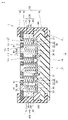
- FIG. 1 is a schematic vertical cross-sectional view showing the configuration of a semiconductor device according to a first embodiment
- FIG. FIG. 2 is a schematic vertical cross-sectional view showing the configuration of electrode terminals of the semiconductor device according to the first embodiment
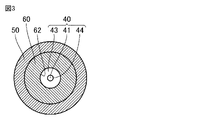
- FIG. 3 is a schematic cross-sectional view taken along line III-III of FIG. 2
- FIG. 2 is a flowchart schematically showing a method of manufacturing a semiconductor device according to Embodiment 1; It is a vertical cross-sectional schematic diagram which shows the process which engages a positioning jig with an engaging part. It is a vertical cross-sectional schematic diagram which shows the process of making a ball
- FIG. 7 is a schematic vertical cross-sectional view showing the configuration of an electrode terminal according to Embodiment 2;
- FIG. 11 is a schematic vertical cross-sectional view showing the configuration of an electrode terminal according to Embodiment 3;
- FIG. 10 is a schematic vertical cross-sectional view showing the configuration of an electrode terminal according to Embodiment 4;
- FIG. 11 is a schematic vertical cross-sectional view showing the configuration of an electrode terminal according to Embodiment 5;
- FIG. 11 is a schematic vertical cross-sectional view showing a configuration of an electrode terminal according to a modification of Embodiment 5;
- FIG. 12 is a schematic vertical cross-sectional view showing the configuration of an electrode terminal according to Embodiment 6;
- FIG. 11 is a schematic vertical cross-sectional view showing the configuration of an electrode terminal according to Embodiment 7;
- FIG. 16 is a view showing a state in which the ball in the electrode terminal of FIG. 15 has rotated by a certain angle;
- FIG. 12 is a schematic vertical cross-sectional view showing a configuration of an electrode terminal according to a modification of Embodiment 7;
- FIG. 18 is a view showing a state in which the ball in the electrode terminal of FIG. 17 has rotated by a certain angle;
- FIG. 11 is a schematic vertical cross-sectional view showing the configuration of an electrode terminal according to Embodiment 8;
- FIG. 20 is a schematic cross-sectional view showing the configuration of an electrode terminal according to Embodiment 9
- FIG. 1 is a schematic vertical cross-sectional view showing the configuration of a semiconductor device 1 according to Embodiment 1.
- the semiconductor device 1 mainly includes electrode terminals 200, a circuit board 110, a semiconductor element 20, a first electrode 81, a second electrode 31, a base plate 10, and a case . have in The electrode terminal 200 has a ball 40 , a support member 140 and an elastic body 71 . The details of the configuration of the electrode terminal 200 will be described later.
- the circuit board 110 is arranged above the electrode terminals 200 .
- the circuit board 110 has a substantially flat plate shape.
- the circuit board 110 has a first surface 112 and a first back surface 111 .
- the first back surface 111 is located opposite the first surface 112 .
- the circuit board 110 is provided with a first through hole 114 penetrating through the first surface 112 and the first back surface 111 .
- the first electrode 81 is inside the first through hole 114 .
- the first electrode 81 is connected with the electrode terminal 200 . More specifically, the first electrode 81 and the electrode terminal 200 may be threaded so as to be fastened together.
- the semiconductor element 20 is arranged below the electrode terminals 200 .
- the semiconductor element 20 has a substantially flat plate shape.
- Semiconductor element 20 has a second surface 21 and a second back surface 22 .
- the second surface 21 is arranged to face the first back surface 111 of the circuit board 110 .
- the second back surface 22 is located opposite the second surface 21 .
- a second electrode 31 is provided on the second surface 21 .
- the second electrode 31 is in direct contact with the ball 40 of the electrode terminal 200 .
- the second electrode 31 is electrically connected to the first electrode 81 via the electrode terminal 200 .
- the base plate 10 has a third surface 13 and a third back surface 14 .
- the base plate 10 is arranged below the semiconductor element 20 .
- the third surface 13 is in contact with the second back surface 22 .
- the third back surface 14 is located opposite the third front surface 13 .
- the case 130 fixes the circuit board 110 and the base plate 10 so as to sandwich them from both sides.
- the semiconductor device 1 further has a third electrode 80 , a fourth electrode 30 , a plate electrode 90 , a block electrode 100 , a compression coil spring 70 and a positioning plate 120 .
- the circuit board 110 is provided with a second through hole 115 passing through the first surface 112 and the first back surface 111 .
- the third electrode 80 is inside the second through hole 115 .
- a fourth electrode 30 is provided on the second surface 21 of the semiconductor element 20 .
- the plate electrode 90 is arranged on the fourth electrode 30 .
- the block electrode 100 is sandwiched between the plate electrode 90 and the third electrode 80 .
- the block electrode 100 is cylindrical.
- the compression coil spring 70 is arranged inside the block electrode 100 .
- the compression coil spring 70 is sandwiched between the plate electrode 90 and the third electrode 80 .
- the third electrode 80 is electrically connected to the fourth electrode 30 via the plate electrode 90 and block electrode 100 .
- the third electrode 80 may be electrically connected to the fourth electrode 30 via the plate electrode 90 and the compression coil spring 70 .
- the positioning plate 120 positions the semiconductor element 20 .
- the positioning plate 120 is made of resin, for example.
- the positioning plate 120 is arranged on the side surface of the semiconductor element 20 .
- the base plate 10 further has grooves 11 .
- the groove portion 11 is provided on the side surface of the base plate 10 .
- the case 130 has a first protrusion 132 , a second protrusion 133 and a third protrusion 134 .
- the first convex portion 132 and the second convex portion 133 sandwich the circuit board 110 vertically.
- the first protrusion 132 is in contact with the first surface 112 .
- Second convex portion 133 is in contact with each of first rear surface 111 and positioning plate 120 .
- the third protrusion 134 is inserted into the groove 11 of the base plate 10 .
- the first convex portion 132 and the third convex portion 134 vertically sandwich the circuit board 110 and the base plate 10 .
- a pressing force is applied to the first surface 112 of the circuit board 110 by the first protrusion 132 .
- the pressure contact force is a force in the direction from the first surface 112 toward the first back surface 111 .
- the compression coil spring 70 is compressed by the pressing force.
- the third electrode 80 transmits pressure contact force to the fourth electrode 30 via the block electrode 100 and the plate electrode 90 .
- the first electrode 81 transmits pressure contact force to the second electrode 31 via the electrode terminal 200 .
- FIG. 2 is a schematic vertical cross-sectional view showing the configuration of the electrode terminals of the semiconductor device according to the first embodiment.
- the ball 40 of the electrode terminal 200 is conductive.
- Ball 40 has a surface 43 .
- the surface 43 constitutes a spherical surface.
- Support member 140 supports ball 40 .
- the support member 140 has electrical conductivity.
- the support member 140 has a pressing portion 60 and a tubular portion 50 .
- the pressing part 60 is arranged above the ball 40 .
- the holding portion 60 is, for example, cylindrical.
- the pressing portion 60 has a first upper end surface 68 , a first lower end surface 69 , a first inner wall surface 62 , a first outer wall surface 61 and a first corner portion 63 .
- the first lower end surface 69 is provided on the opposite side of the first upper end surface 68 .
- the first outer wall surface 61 is provided outside the first inner wall surface 62 .
- the first corner portion 63 is the boundary between the first inner wall surface 62 and the first lower end surface 69 .
- the first corner 63 is in contact with the ball 40 .
- the tubular portion 50 surrounds each of the pressing portion 60 and the ball 40 .
- the tubular portion 50 has a tubular portion 51 , a second upper end surface 55 , a second lower end surface 56 , a support portion 52 , a second inner wall surface 54 and a second outer wall surface 53 .
- the cylindrical portion 51 has a cylindrical shape.
- the second lower end surface 56 is provided on the opposite side of the second upper end surface 55 .
- the support portion 52 extends inward along the second lower end surface 56 .
- the support portion 52 protrudes inward from the second inner wall surface 54 .
- the support portion 52 is cylindrical.
- the second inner wall surface 54 is arranged along the first outer wall surface 61 of the pressing portion 60 .
- the second outer wall surface 53 is provided on the opposite side of the second inner wall surface 54 .
- the ball 40 is arranged so as to fit into the hole formed by the support portion 52 . That is, the support portion 52 is in contact with the ball 40 .
- the elastic body 71 is in contact with the first upper end face 68 of the pressing portion 60 . That is, the pressing portion 60 is sandwiched between the elastic body 71 and the ball 40 .
- the elastic body 71 is arranged inside the tubular portion 50 .
- the elastic body 71 is, for example, a compression coil spring.
- the elastic body 71 presses the ball 40 against the second electrode 31 via the pressing portion 60 .
- the elastic body 71 may press the ball 40 against the support portion 52 via the pressing portion 60 .
- a second upper end face 55 of the tubular portion 50 is connected to the first electrode 81 of the circuit board 110 .
- the first electrode 81 and the cylindrical portion 50 may be threaded so that they can be fastened together.
- the upper end of the elastic body 71 is in contact with the first electrode 81 .
- Ball 40 is electrically connected to first electrode 81 via cylindrical portion 50 , pressing portion 60 and elastic body 71 .
- Ball 40 is electrically connected to second electrode 31 of semiconductor element 20 .
- An engaging portion 41 is provided on at least part of the surface 43 of the ball 40 .
- the engaging portion 41 has, for example, a convex shape.
- the engagement portion 41 may be cylindrical.
- the engaging portion 41 may have a polygonal prism shape.
- the engaging portion 41 has side surfaces 44 .
- the side surface 44 is continuous with the surface 43 of the ball 40 .
- An engaged portion corresponding to the engaging portion 41 is provided in the pressing portion 60 .
- the engaged portion is, for example, the first inner wall surface 62 of the pressing portion 60 .
- the first inner wall surface 62 forms, for example, a cylindrical hole.
- FIG. 3 is a schematic cross-sectional view taken along line III-III in FIG.
- the cross section shown in FIG. 3 is perpendicular to the direction in which the ball 40 is pressed against the second electrode 31 .
- the engaging portion 41 is arranged at the center of the first inner wall surface 62 of the pressing portion 60 .
- the side surface 44 of the engaging portion 41 is arranged so as to come into contact with the first inner wall surface 62, which is the engaged portion, when the ball 40 rotates by a certain angle.
- the first inner wall surface 62 forms, for example, a circular hole.
- the pressing portion 60 has, for example, an annular shape.
- the tubular portion 50 has, for example, an annular shape. The tubular portion 50 surrounds the pressing portion 60 .
- the pressing portion 60 surrounds the engaging portion 41 .
- FIG. 4 is a flow diagram schematically showing the method of manufacturing the semiconductor device according to the first embodiment.
- the method of manufacturing the semiconductor device according to the first embodiment comprises a step of engaging positioning jig 42 with engaging portion 41 (S10), and connecting ball 40 to an electrode on semiconductor element 20. It mainly includes a contact step (S20), a step of attaching the case 130 (S30), and a step of removing the positioning jig 42 (S40).
- FIG. 5 is a schematic vertical cross-sectional view showing a process of engaging the positioning jig 42 with the engaging portion 41.
- a circuit board 110 to which electrode terminals 200 are attached is prepared.
- a first through hole 114 , a second through hole 115 , and a third through hole 113 are formed in the circuit board 110 .
- the first electrode 81 and the third electrode 80 are inside the first through hole 114 and the second through hole 115 of the circuit board 110, respectively.
- the first electrode 81 may be attached to the first through hole 114 by press fitting.
- the third electrode 80 may be attached to the second through hole 115 by press fitting.
- the electrode terminal 200 is connected with the first electrode 81 .
- the first electrode 81 and the electrode terminal 200 may be threaded so as to be fastened together.
- the first electrode 81 may be perforated so that the electrode terminal 200 can be press-fitted.
- the circuit board 110 is arranged so that the electrode terminals 200 are positioned above.
- the engaging portion 41 of the ball 40 is arranged in a direction facing the first rear surface 111 of the circuit board 110 by gravity.
- the positioning jig 42 has, for example, a rod-shaped portion 46 and a second recess 47 provided in the rod-shaped portion 46 .
- the positioning jig 42 is inserted into the electrode terminal 200 through the third through hole 113 of the circuit board 110 .
- the engaging portion 41 of the ball 40 engages with the second recessed portion 47 of the positioning jig 42 . This positions the ball 40 so that it does not rotate.
- a plurality of positioning jigs 42 may be connected together. This makes it easier to insert the positioning jig 42 into the electrode terminal 200 .
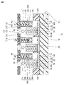
- FIG. 6 is a schematic vertical cross-sectional view showing the process of bringing the ball 40 into contact with the electrode on the semiconductor element 20.
- a base plate 10 provided with a semiconductor element 20 and a second electrode 31 is prepared.
- the third surface 13 of the base plate 10 is in contact with the second back surface 22 of the semiconductor element 20 .
- a second electrode 31 and a fourth electrode 30 are provided on the second surface 21 of the semiconductor element 20 .
- a plate electrode 90 is arranged on the fourth electrode 30 .
- Block electrode 100 and compression coil spring 70 are arranged on plate electrode 90 .
- the positioning plate 120 positions the semiconductor element 20 .
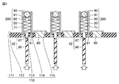
- the circuit board 110 is inverted from the state shown in FIG. Ball 40 is arranged to face second electrode 31 . A pressure contact force is then applied to the circuit board 110 . Circuit board 110 moves in the direction of the arrow. The ball 40 contacts the second electrode 31 while the engaging portion 41 is engaged with the positioning jig 42 . The third electrode 80 contacts each of the block electrode 100 and the compression coil spring 70 . The compression coil spring 70 and the elastic body 71 are in a compressed state.
- FIG. 7 is a schematic vertical cross-sectional view showing the process of attaching the case 130.
- the case 130 sandwiches the circuit board 110 and the base plate 10 from both sides.
- the case 130 has a first protrusion 132 , a second protrusion 133 and a third protrusion 134 .
- the first convex portion 132 and the second convex portion 133 sandwich the circuit board 110 vertically.
- the third protrusion 134 is inserted into the groove 11 of the base plate 10 .
- the circuit board 110 is pressed against the first protrusion 132 from above.
- circuit board 110 receives an elastic force from each of compression coil spring 70 and elastic body 71 .
- the elastic force is a force in the direction from the first back surface 111 of the circuit board 110 toward the first surface 112 .
- FIG. 8 is a schematic vertical cross-sectional view showing the process of removing the positioning jig 42.
- the positioning jig 42 is removed.
- the positioning jig 42 may be removed by pulling it upward from the semiconductor device 1 .
- the positioning jig 42 may be removed by turning the semiconductor device 1 upside down and dropping it using gravity.
- the third through hole 113 formed in the circuit board 110 may be closed. As a result, it is possible to prevent foreign matter from entering the interior of the electrode terminal 200 through the third through hole 113 . Therefore, it is possible to prevent foreign matter from staying at the contact portion between the ball 40 and the pressing portion 60 or the contact portion between the ball 40 and the cylindrical portion 50 . Therefore, it is possible to prevent the foreign matter from hindering the rotation of the ball 40 .
- Embodiment 1 When a shearing force is applied to the semiconductor device 1 , relative displacement in the shearing direction occurs between the electrode terminals 200 and the semiconductor element 20 . At this time, the ball 40 rotates while contacting the second electrode 31 of the semiconductor element 20 . As the shear force increases, the rotation angle of the ball 40 increases. Shear force is a force in a direction perpendicular to the pressure contact force. Shear forces are generated, for example, by temperature cycling or vibration.
- the engaging portion 41 is provided on the surface 43 of the ball 40 .
- the support member 140 is provided with a first inner wall surface 62 as an engaged portion.
- engaging portion 41 comes into contact with first inner wall surface 62 after ball 40 rotates by a certain angle. This stops the rotation of the ball 40 .
- the frictional force between the ball 40 and the second electrode 31 of the semiconductor element 20 increases. Therefore, separation between the ball 40 and the second electrode 31 is prevented. Therefore, it is possible to suppress the occurrence of poor conduction between the ball 40 and the second electrode 31 .
- the ball 40 If the ball 40 is not provided with the engaging portion 41, the ball 40 rolls endlessly. Therefore, in order to prevent the ball 40 and the second electrode 31 from separating, it is necessary to increase the size of the second electrode 31 . According to the electrode terminal 200 according to Embodiment 1, the rolling range of the ball 40 can be restricted according to the size of the second electrode 31 . Therefore, the electrode terminal 200 according to the first embodiment can reduce the size of the semiconductor device 1 compared to the case where the engaging portion 41 is not provided.
- the electrode terminal 200 according to Embodiment 1 when the magnitude of the shearing force is less than a certain value, the rotation angle of the ball 40 is small, so the engaging portion 41 and the first inner wall surface 62 do not come into contact with each other. Therefore, the ball 40 rolls on the second electrode 31 of the semiconductor element 20 . If the electrode terminal 200 does not have the ball 40, the electrode terminal 200 and the second electrode 31 rub against each other at the contact portion. Therefore, the electrode terminal 200 according to Embodiment 1 can suppress the friction applied to the second electrode 31 as compared with the case where the ball 40 is not provided. Therefore, damage to the second electrode 31 can be prevented. Therefore, poor conduction can be prevented between the ball 40 and the second electrode 31 .
- the electrode terminal 200 has the elastic body 71 arranged to press the ball 40 against the support member 140 . Therefore, the ball 40 can be pressed against the second electrode 31 of the semiconductor element 20 more strongly.
- the support member 140 has the pressing portion 60 sandwiched between the elastic body 71 and the ball 40 .
- a lower end of the elastic body 71 is in contact with the first upper end surface 68 of the pressing portion 60 .
- the first upper end surface 68 is substantially flat.
- the lower end of the elastic body 71 is in contact with the surface 43 of the ball 40 .
- Surface 43 is spherical. Therefore, the lower end of the elastic body 71 deforms along the surface 43 . Therefore, in the electrode terminal 200 according to Embodiment 1, deformation of the elastic body 71 is suppressed as compared with the case where the support member 140 does not have the pressing portion 60 . Therefore, the elastic body 71 can stably press the ball 40 against the second electrode 31 .
- the support member 140 has the tubular portion 50 surrounding the pressing portion 60 and the ball 40 .
- the displacement of the pressing portion 60 in the shear direction is suppressed by the cylindrical portion 50 . Therefore, the ball 40 can be stably pressed against the second electrode 31 .
- the engaged portion is the first inner wall surface 62 of the pressing portion 60 .
- the first inner wall surface 62 forms a cylindrical hole.
- the diameter of the hole formed by the first inner wall surface 62 can be easily changed during manufacturing.
- the rotation angle range of the ball 40 is changed. Therefore, when the first inner wall surface 62 forms a cylindrical hole, the range of rotation angle of the ball 40 can be easily changed. This makes it possible to easily change the range of the rotation angle of the ball 40 according to the size of the second electrode 31 .
- only one electrode terminal 200 among the plurality of electrode terminals 200 can reduce the range of the rotation angle of the ball 40 .
- the smaller the range of the rotation angle of the ball 40 the easier it is for the ball 40 to stop rotating.
- the frictional force increases between the ball 40 and the second electrode 31 .
- the contact portion between the ball 40 and the second electrode 31 wears, shortening the time (remaining life) until conduction failure occurs. Therefore, the life of only one semiconductor element 20 among the plurality of semiconductor elements 20 can be shortened.
- a plurality of combinations of electrode terminals 200 and semiconductor elements 20 are prepared.
- the diameter of the hole formed by the first inner wall surface 62 of the electrode terminal 200 is different for each.
- the remaining life of the semiconductor device 1 can be estimated by acquiring the relationship between the hole diameter and the number of loads until the conduction failure occurs.
- the material of the ball 40 and the engaging portion 41 may be, for example, a metal-plated rubber material. However, when designing the range of the rotation angle of the ball 40, it is necessary to consider deformation due to contact between the engaging portion 41 and the engaged portion. Therefore, the material of the ball 40 and the engaging portion 41 is preferably metal.
- Embodiment 2 Next, an electrode terminal according to Embodiment 2 will be described. In the following, differences from the electrode terminals according to Embodiment 1 will be mainly described, and similar descriptions will not be repeated.
- FIG. 9 is a vertical cross-sectional schematic diagram showing the configuration of the electrode terminal 200 according to the second embodiment.
- the first concave portion 45 is an engaging portion. That is, the engaging portion may be concave. It is desirable that the first recess 45 constitutes a cylindrical hole.
- the pressing portion 60 has a fourth convex portion 66 .
- the fourth convex portion 66 is an engaged portion. At least part of the fourth protrusion 66 is located inside the first recess 45 .
- the fourth convex portion 66 is provided on the first lower end surface 69 .
- the fourth convex portion 66 contacts the inner wall surface forming the first concave portion 45 of the ball 40 when the ball 40 rotates more than a certain amount.
- the electrode terminal according to the second embodiment can also obtain the same effect as the electrode terminal according to the first embodiment.
- Embodiment 3 Next, an electrode terminal according to Embodiment 3 will be described. In the following, differences from the electrode terminals according to Embodiment 1 will be mainly described, and similar descriptions will not be repeated.
- FIG. 10 is a schematic vertical cross-sectional view showing the configuration of the electrode terminal 200 according to Embodiment 3.
- the engaging portion 41 may have a first portion 151 and a second portion 152 .
- the engaged portion is the first lower end surface 69 of the pressing portion 60 .
- Each of the first portion 151 and the second portion 152 is arranged between the first lower end surface 69 of the pressing portion 60 and the second inner wall surface 54 of the tubular portion 50 .
- the pressing portion 60 of the electrode terminal 200 according to Embodiment 3 does not have a hole. Therefore, foreign matter can be prevented from entering through the hole of the pressing portion 60 from above. Therefore, it is possible to prevent foreign matter from staying at the contact portion between the ball 40 and the pressing portion 60 or the contact portion between the ball 40 and the cylindrical portion 50 . As a result, it is possible to prevent the foreign matter from hindering the rotation of the ball 40 .
- Embodiment 4 Next, an electrode terminal according to Embodiment 4 will be described. In the following, differences from the electrode terminals according to Embodiment 1 will be mainly described, and similar descriptions will not be repeated.
- FIG. 11 is a schematic vertical cross-sectional view showing the configuration of the electrode terminal 200 according to Embodiment 4.
- the engaging portion 41 may have a first portion 151 and a second portion 152 .
- the engaged portion may be provided on the tubular portion 50 .
- the engaged portion is the second lower end surface 56 of the tubular portion 50 .
- Each of first portion 151 and second portion 152 is arranged between semiconductor element 20 and second lower end surface 56 of cylindrical portion 50 .
- Each of the first portion 151 and the second portion 152 is desirably arranged so as not to contact the second electrode 31 when the ball 40 rotates.
- the pressing portion 60 of the electrode terminal 200 according to Embodiment 4 does not have a hole.
- the electrode terminal according to Embodiment 4 is not limited to the configuration described above.
- the electrode terminal according to Embodiment 4 may not have the pressing portion 60, for example.
- the ball contacts the elastic body 71 .
- the electrode terminal according to Embodiment 4 may not have the elastic body 71, for example.
- the pressing portion 60 may be in contact with the first rear surface 111 of the circuit board 110 .
- the electrode terminal according to Embodiment 4 may not have both the elastic body 71 and the pressing portion 60, for example.
- ball 40 may be in direct contact with first back surface 111 .
- Ball 40 may be in direct contact with first electrode 81 .
- Embodiment 5 Next, an electrode terminal according to Embodiment 5 will be described. In the following, differences from the electrode terminals according to Embodiment 1 will be mainly described, and similar descriptions will not be repeated.
- FIG. 12 is a schematic vertical cross-sectional view showing the configuration of the electrode terminal 200 according to Embodiment 5.
- FIG. FIG. 13 is a schematic vertical cross-sectional view showing the configuration of an electrode terminal 200 according to a modification of the fifth embodiment.
- the elastic body 71 may be a disc spring.
- six disc springs 72 are stacked in series.
- six disc springs 72 are stacked in parallel.
- the disc springs 72 may be stacked in a combination of series and parallel.
- the electrode terminal according to the fifth embodiment and the electrode terminal according to the modification of the fifth embodiment can also obtain the same effect as the electrode terminal according to the first embodiment.
- Embodiment 6 Next, an electrode terminal according to Embodiment 6 will be described. In the following, differences from the electrode terminals according to Embodiment 1 will be mainly described, and similar descriptions will not be repeated.
- FIG. 14 is a schematic vertical cross-sectional view showing the configuration of the electrode terminal 200 according to Embodiment 6.
- the pressing portion 60 may have the first concave spherical surface 2 .
- the first concave spherical surface 2 continues to each of the first inner wall surface 62 and the first lower end surface 69 .
- the first concave spherical surface 2 follows the contour of the ball 40 .
- the first concave spherical surface 2 is in surface contact with the ball 40 . Therefore, wear of the contact portion between the ball 40 and the pressing portion 60 can be suppressed. Furthermore, the electrical connection between the ball 40 and the pressing portion 60 becomes more stable.
- the tubular portion 50 may have a second concave spherical surface 58 .
- the second concave spherical surface 58 is provided on the support portion 52 .
- the second concave spherical surface 58 follows the contour of the ball 40 .
- the second concave spherical surface 58 is in surface contact with the ball 40 . Therefore, wear of the contact portion between the ball 40 and the cylindrical portion 50 can be suppressed.
- the electrical connection between the ball 40 and the tubular portion 50 is more stable.
- Embodiment 7 Next, an electrode terminal according to Embodiment 7 will be described. In the following, differences from the electrode terminals according to Embodiment 1 will be mainly described, and similar descriptions will not be repeated.
- FIG. 15 is a schematic vertical cross-sectional view showing the configuration of the electrode terminal 200 according to Embodiment 7.
- FIG. FIG. 16 is a diagram showing a state in which the ball 40 in the electrode terminal 200 of FIG. 15 is rotated by a certain angle.
- the engaging portion 41 may be conical.
- the side surface 44 of the engaging portion 41 and the first inner wall surface 62 of the pressing portion 60 are in line contact. Therefore, the contact area between the engaging portion 41 and the first inner wall surface 62 increases compared to when the engaging portion 41 has a cylindrical shape. Therefore, wear of the contact portion between the engaging portion 41 and the first inner wall surface 62 can be suppressed.
- FIG. 17 is a vertical cross-sectional schematic diagram showing the configuration of an electrode terminal 200 according to a modification of Embodiment 7.
- the first inner wall surface 62 of the pressing portion 60 may be configured to have a mortar shape. From another point of view, the hole formed by the first inner wall surface 62 may have a truncated cone shape. The cross-sectional area of the hole formed by the first inner wall surface 62 may be smaller on the first lower end surface 69 side than on the first upper end surface 68 side.
- the engaging portion 41 has a cylindrical shape.
- FIG. 18 is a diagram showing a state in which the ball 40 in the electrode terminal 200 of FIG. 17 has been rotated by a certain angle. As shown in FIG. 18, when the ball 40 rotates by a certain angle, the side surface 44 of the engaging portion 41 and the first inner wall surface 62 of the pressing portion 60 are in line contact. Therefore, the electrode terminal 200 according to the modification of the seventh embodiment can also obtain the same effect as the electrode terminal according to the seventh embodiment.
- Embodiment 8 Next, an electrode terminal according to Embodiment 8 will be described. In the following, differences from the electrode terminals according to Embodiment 1 will be mainly described, and similar descriptions will not be repeated.
- FIG. 19 is a schematic vertical cross-sectional view showing the configuration of an electrode terminal 200 according to Embodiment 8.
- the pressing portion 60 may have a first member 64 and a second member 65 .
- the first member 64 contacts the ball 40 .
- the second member 65 is tubular.
- a second member 65 extends from the first member 64 opposite the ball 40 .
- the second member 65 is arranged to surround the elastic body 71 .
- the first member 64 constitutes a first lower end surface 69 .
- the second member 65 constitutes a third upper end surface 67 .
- the third upper end face 67 is arranged to face the first electrode 81 .
- the third upper end surface 67 and the first electrode 81 are slightly separated from each other when no upward force is applied to the semiconductor device 1 in a cross-sectional view.
- the pressing portion 60 has the second member 65 , the third upper end surface 67 of the pressing portion 60 comes into contact with the first electrode 81 when the pressing portion 60 is displaced upward by a certain distance. Therefore, the pressing portion 60 stops. That is, the pressing portion 60 has a limited range of upward displacement. Accordingly, the upward displacement range of the ball 40 is similarly limited. This can prevent the ball 40 and the second electrode 31 from being separated from each other.
- Embodiment 9 Next, an electrode terminal according to Embodiment 9 will be described. In the following, differences from the electrode terminals according to Embodiment 1 will be mainly described, and similar descriptions will not be repeated.
- FIG. 20 is a schematic cross-sectional view showing the configuration of an electrode terminal 200 according to Embodiment 9.
- the schematic cross-sectional view shown in FIG. 20 corresponds to the schematic cross-sectional view shown in FIG.
- the outer shape of the cylindrical portion 50 may be a polygonal prism shape. More specifically, the outer shape of the tubular portion 50 may be a quadrangular prism shape or a hexagonal prism shape.
- the space around the electrode terminal 200 can be used more efficiently than when the outer shape of the tubular portion 50 is a columnar shape.
- the thickness of the cylindrical portion 50 can be increased. Thereby, the strength of the tubular portion 50 can be increased. Furthermore, the stability of electrical connection between the first electrode 81 and the ball 40 via the cylindrical portion 50 is improved.
Landscapes
- Connecting Device With Holders (AREA)
- Coupling Device And Connection With Printed Circuit (AREA)
- Measuring Leads Or Probes (AREA)
Priority Applications (3)
| Application Number | Priority Date | Filing Date | Title |
|---|---|---|---|
| PCT/JP2021/019177 WO2022244194A1 (ja) | 2021-05-20 | 2021-05-20 | 電極端子、半導体装置および半導体装置の製造方法 |
| DE112021007682.5T DE112021007682T5 (de) | 2021-05-20 | 2021-05-20 | Elektrodenanschluss, halbleitereinrichtung und verfahren zum herstellen einer halbleitereinrichtung |
| JP2023522124A JP7515715B2 (ja) | 2021-05-20 | 2021-05-20 | 電極端子、半導体装置および半導体装置の製造方法 |
Applications Claiming Priority (1)
| Application Number | Priority Date | Filing Date | Title |
|---|---|---|---|
| PCT/JP2021/019177 WO2022244194A1 (ja) | 2021-05-20 | 2021-05-20 | 電極端子、半導体装置および半導体装置の製造方法 |
Publications (1)
| Publication Number | Publication Date |
|---|---|
| WO2022244194A1 true WO2022244194A1 (ja) | 2022-11-24 |
Family
ID=84141552
Family Applications (1)
| Application Number | Title | Priority Date | Filing Date |
|---|---|---|---|
| PCT/JP2021/019177 Ceased WO2022244194A1 (ja) | 2021-05-20 | 2021-05-20 | 電極端子、半導体装置および半導体装置の製造方法 |
Country Status (3)
| Country | Link |
|---|---|
| JP (1) | JP7515715B2 (https=) |
| DE (1) | DE112021007682T5 (https=) |
| WO (1) | WO2022244194A1 (https=) |
Citations (3)
| Publication number | Priority date | Publication date | Assignee | Title |
|---|---|---|---|---|
| JPH0316075U (https=) * | 1989-06-29 | 1991-02-18 | ||
| JP2000331141A (ja) * | 1999-05-17 | 2000-11-30 | Sony Corp | 情報記録媒体および情報記録媒体を備える電子機器 |
| JP2013051052A (ja) * | 2011-08-30 | 2013-03-14 | Denso Corp | 脱着接続構造 |
-
2021
- 2021-05-20 DE DE112021007682.5T patent/DE112021007682T5/de active Pending
- 2021-05-20 JP JP2023522124A patent/JP7515715B2/ja active Active
- 2021-05-20 WO PCT/JP2021/019177 patent/WO2022244194A1/ja not_active Ceased
Patent Citations (3)
| Publication number | Priority date | Publication date | Assignee | Title |
|---|---|---|---|---|
| JPH0316075U (https=) * | 1989-06-29 | 1991-02-18 | ||
| JP2000331141A (ja) * | 1999-05-17 | 2000-11-30 | Sony Corp | 情報記録媒体および情報記録媒体を備える電子機器 |
| JP2013051052A (ja) * | 2011-08-30 | 2013-03-14 | Denso Corp | 脱着接続構造 |
Also Published As
| Publication number | Publication date |
|---|---|
| DE112021007682T5 (de) | 2024-02-29 |
| JPWO2022244194A1 (https=) | 2022-11-24 |
| JP7515715B2 (ja) | 2024-07-12 |
Similar Documents
| Publication | Publication Date | Title |
|---|---|---|
| US8632369B2 (en) | Terminal connecting device for energy storage module | |
| KR101288274B1 (ko) | 콘택트 프로브 및 그것을 구비한 반도체 소자용 소켓 | |
| KR102166677B1 (ko) | 멤스 포고 핀 및 이를 이용한 검사 방법 | |
| KR101715750B1 (ko) | 반도체 디바이스를 검사하기 위한 프로브 및 그를 사용하는 테스트 소켓 | |
| KR101704710B1 (ko) | 검사장치용 프로브 | |
| CN101496458A (zh) | 用于将电气或电子部件、尤其是印刷电路板固定在壳体中的方法及其固定元件 | |
| KR101493901B1 (ko) | 반도체 패키지 테스트용 유연성 실리콘 부싱 소켓 | |
| KR102473943B1 (ko) | 테스트 소켓용 핀 및 이를 포함하는 테스트 소켓 | |
| JP2008535175A (ja) | 密閉型バッテリー用ケーシング | |
| JP2024511510A (ja) | プローブコンタクト | |
| US10488439B2 (en) | Compressible layer with integrated bridge in IC testing apparatus | |
| JPH08203644A (ja) | Lsiパッケージ用ソケット | |
| US8926343B2 (en) | Electrical interconnect device employing an array of conductive elastomer columns | |
| KR102121754B1 (ko) | 상하 2개의 영역으로 구분되는 단일 코일 스프링을 포함하는 테스트 소켓 | |
| WO2022244194A1 (ja) | 電極端子、半導体装置および半導体装置の製造方法 | |
| US9017859B2 (en) | Secondary battery structure | |
| US10473713B2 (en) | Interposer block with retractable spring pin top cover plate | |
| JP2009158404A (ja) | コンタクト部材及びコンタクト部材の接続方法及びソケット | |
| JP7274853B2 (ja) | コンタクトピンおよびソケット | |
| JP5636908B2 (ja) | ソケットおよび電子装置 | |
| KR102170384B1 (ko) | 멤스 플런저를 이용하여 콘택 공차 범위가 확장되는 포고 핀 | |
| CN211047393U (zh) | 加压组件 | |
| JP2004257831A (ja) | 接触子及び電気的接続装置 | |
| KR20060088416A (ko) | 프로브 유닛의 평탄화 장치 | |
| TWM511948U (zh) | 壓合機構 |
Legal Events
| Date | Code | Title | Description |
|---|---|---|---|
| 121 | Ep: the epo has been informed by wipo that ep was designated in this application |
Ref document number: 21940808 Country of ref document: EP Kind code of ref document: A1 |
|
| WWE | Wipo information: entry into national phase |
Ref document number: 2023522124 Country of ref document: JP |
|
| WWE | Wipo information: entry into national phase |
Ref document number: 112021007682 Country of ref document: DE |
|
| 122 | Ep: pct application non-entry in european phase |
Ref document number: 21940808 Country of ref document: EP Kind code of ref document: A1 |