WO2022209119A1 - 半導体加工用粘着テープおよび半導体装置の製造方法 - Google Patents
半導体加工用粘着テープおよび半導体装置の製造方法 Download PDFInfo
- Publication number
- WO2022209119A1 WO2022209119A1 PCT/JP2022/000573 JP2022000573W WO2022209119A1 WO 2022209119 A1 WO2022209119 A1 WO 2022209119A1 JP 2022000573 W JP2022000573 W JP 2022000573W WO 2022209119 A1 WO2022209119 A1 WO 2022209119A1
- Authority
- WO
- WIPO (PCT)
- Prior art keywords
- adhesive tape
- meth
- buffer layer
- semiconductor
- semiconductor wafer
- Prior art date
- Legal status (The legal status is an assumption and is not a legal conclusion. Google has not performed a legal analysis and makes no representation as to the accuracy of the status listed.)
- Ceased
Links
Images


Classifications
-
- B—PERFORMING OPERATIONS; TRANSPORTING
- B32—LAYERED PRODUCTS
- B32B—LAYERED PRODUCTS, i.e. PRODUCTS BUILT-UP OF STRATA OF FLAT OR NON-FLAT, e.g. CELLULAR OR HONEYCOMB, FORM
- B32B27/00—Layered products comprising a layer of synthetic resin
- B32B27/06—Layered products comprising a layer of synthetic resin as the main or only constituent of a layer, which is next to another layer of the same or of a different material
- B32B27/08—Layered products comprising a layer of synthetic resin as the main or only constituent of a layer, which is next to another layer of the same or of a different material of synthetic resin
-
- B—PERFORMING OPERATIONS; TRANSPORTING
- B32—LAYERED PRODUCTS
- B32B—LAYERED PRODUCTS, i.e. PRODUCTS BUILT-UP OF STRATA OF FLAT OR NON-FLAT, e.g. CELLULAR OR HONEYCOMB, FORM
- B32B27/00—Layered products comprising a layer of synthetic resin
- B32B27/30—Layered products comprising a layer of synthetic resin comprising vinyl (co)polymers; comprising acrylic (co)polymers
- B32B27/308—Layered products comprising a layer of synthetic resin comprising vinyl (co)polymers; comprising acrylic (co)polymers comprising acrylic (co)polymers
-
- B—PERFORMING OPERATIONS; TRANSPORTING
- B32—LAYERED PRODUCTS
- B32B—LAYERED PRODUCTS, i.e. PRODUCTS BUILT-UP OF STRATA OF FLAT OR NON-FLAT, e.g. CELLULAR OR HONEYCOMB, FORM
- B32B27/00—Layered products comprising a layer of synthetic resin
- B32B27/36—Layered products comprising a layer of synthetic resin comprising polyesters
-
- C—CHEMISTRY; METALLURGY
- C09—DYES; PAINTS; POLISHES; NATURAL RESINS; ADHESIVES; COMPOSITIONS NOT OTHERWISE PROVIDED FOR; APPLICATIONS OF MATERIALS NOT OTHERWISE PROVIDED FOR
- C09J—ADHESIVES; NON-MECHANICAL ASPECTS OF ADHESIVE PROCESSES IN GENERAL; ADHESIVE PROCESSES NOT PROVIDED FOR ELSEWHERE; USE OF MATERIALS AS ADHESIVES
- C09J133/00—Adhesives based on homopolymers or copolymers of compounds having one or more unsaturated aliphatic radicals, each having only one carbon-to-carbon double bond, and at least one being terminated by only one carboxyl radical, or of salts, anhydrides, esters, amides, imides, or nitriles thereof; Adhesives based on derivatives of such polymers
- C09J133/04—Homopolymers or copolymers of esters
- C09J133/06—Homopolymers or copolymers of esters of esters containing only carbon, hydrogen and oxygen, the oxygen atom being present only as part of the carboxyl radical
- C09J133/062—Copolymers with monomers not covered by C09J133/06
- C09J133/066—Copolymers with monomers not covered by C09J133/06 containing -OH groups
-
- C—CHEMISTRY; METALLURGY
- C09—DYES; PAINTS; POLISHES; NATURAL RESINS; ADHESIVES; COMPOSITIONS NOT OTHERWISE PROVIDED FOR; APPLICATIONS OF MATERIALS NOT OTHERWISE PROVIDED FOR
- C09J—ADHESIVES; NON-MECHANICAL ASPECTS OF ADHESIVE PROCESSES IN GENERAL; ADHESIVE PROCESSES NOT PROVIDED FOR ELSEWHERE; USE OF MATERIALS AS ADHESIVES
- C09J201/00—Adhesives based on unspecified macromolecular compounds
-
- C—CHEMISTRY; METALLURGY
- C09—DYES; PAINTS; POLISHES; NATURAL RESINS; ADHESIVES; COMPOSITIONS NOT OTHERWISE PROVIDED FOR; APPLICATIONS OF MATERIALS NOT OTHERWISE PROVIDED FOR
- C09J—ADHESIVES; NON-MECHANICAL ASPECTS OF ADHESIVE PROCESSES IN GENERAL; ADHESIVE PROCESSES NOT PROVIDED FOR ELSEWHERE; USE OF MATERIALS AS ADHESIVES
- C09J7/00—Adhesives in the form of films or foils
- C09J7/20—Adhesives in the form of films or foils characterised by their carriers
- C09J7/29—Laminated material
-
- C—CHEMISTRY; METALLURGY
- C09—DYES; PAINTS; POLISHES; NATURAL RESINS; ADHESIVES; COMPOSITIONS NOT OTHERWISE PROVIDED FOR; APPLICATIONS OF MATERIALS NOT OTHERWISE PROVIDED FOR
- C09J—ADHESIVES; NON-MECHANICAL ASPECTS OF ADHESIVE PROCESSES IN GENERAL; ADHESIVE PROCESSES NOT PROVIDED FOR ELSEWHERE; USE OF MATERIALS AS ADHESIVES
- C09J7/00—Adhesives in the form of films or foils
- C09J7/30—Adhesives in the form of films or foils characterised by the adhesive composition
- C09J7/38—Pressure-sensitive adhesives [PSA]
- C09J7/381—Pressure-sensitive adhesives [PSA] based on macromolecular compounds obtained by reactions involving only carbon-to-carbon unsaturated bonds
- C09J7/385—Acrylic polymers
-
- H—ELECTRICITY
- H10—SEMICONDUCTOR DEVICES; ELECTRIC SOLID-STATE DEVICES NOT OTHERWISE PROVIDED FOR
- H10P—GENERIC PROCESSES OR APPARATUS FOR THE MANUFACTURE OR TREATMENT OF DEVICES COVERED BY CLASS H10
- H10P52/00—Grinding, lapping or polishing of wafers, substrates or parts of devices
-
- H—ELECTRICITY
- H10—SEMICONDUCTOR DEVICES; ELECTRIC SOLID-STATE DEVICES NOT OTHERWISE PROVIDED FOR
- H10P—GENERIC PROCESSES OR APPARATUS FOR THE MANUFACTURE OR TREATMENT OF DEVICES COVERED BY CLASS H10
- H10P72/00—Handling or holding of wafers, substrates or devices during manufacture or treatment thereof
- H10P72/30—Handling or holding of wafers, substrates or devices during manufacture or treatment thereof for conveying, e.g. between different workstations
-
- H—ELECTRICITY
- H10—SEMICONDUCTOR DEVICES; ELECTRIC SOLID-STATE DEVICES NOT OTHERWISE PROVIDED FOR
- H10P—GENERIC PROCESSES OR APPARATUS FOR THE MANUFACTURE OR TREATMENT OF DEVICES COVERED BY CLASS H10
- H10P72/00—Handling or holding of wafers, substrates or devices during manufacture or treatment thereof
- H10P72/70—Handling or holding of wafers, substrates or devices during manufacture or treatment thereof for supporting or gripping
- H10P72/74—Handling or holding of wafers, substrates or devices during manufacture or treatment thereof for supporting or gripping using temporarily an auxiliary support
- H10P72/7402—Wafer tapes, e.g. grinding or dicing support tapes
-
- H—ELECTRICITY
- H10—SEMICONDUCTOR DEVICES; ELECTRIC SOLID-STATE DEVICES NOT OTHERWISE PROVIDED FOR
- H10P—GENERIC PROCESSES OR APPARATUS FOR THE MANUFACTURE OR TREATMENT OF DEVICES COVERED BY CLASS H10
- H10P72/00—Handling or holding of wafers, substrates or devices during manufacture or treatment thereof
- H10P72/70—Handling or holding of wafers, substrates or devices during manufacture or treatment thereof for supporting or gripping
- H10P72/74—Handling or holding of wafers, substrates or devices during manufacture or treatment thereof for supporting or gripping using temporarily an auxiliary support
- H10P72/7416—Handling or holding of wafers, substrates or devices during manufacture or treatment thereof for supporting or gripping using temporarily an auxiliary support used during dicing or grinding
-
- H—ELECTRICITY
- H10—SEMICONDUCTOR DEVICES; ELECTRIC SOLID-STATE DEVICES NOT OTHERWISE PROVIDED FOR
- H10P—GENERIC PROCESSES OR APPARATUS FOR THE MANUFACTURE OR TREATMENT OF DEVICES COVERED BY CLASS H10
- H10P95/00—Generic processes or apparatus for manufacture or treatments not covered by the other groups of this subclass
-
- C—CHEMISTRY; METALLURGY
- C09—DYES; PAINTS; POLISHES; NATURAL RESINS; ADHESIVES; COMPOSITIONS NOT OTHERWISE PROVIDED FOR; APPLICATIONS OF MATERIALS NOT OTHERWISE PROVIDED FOR
- C09J—ADHESIVES; NON-MECHANICAL ASPECTS OF ADHESIVE PROCESSES IN GENERAL; ADHESIVE PROCESSES NOT PROVIDED FOR ELSEWHERE; USE OF MATERIALS AS ADHESIVES
- C09J2203/00—Applications of adhesives in processes or use of adhesives in the form of films or foils
- C09J2203/326—Applications of adhesives in processes or use of adhesives in the form of films or foils for bonding electronic components such as wafers, chips or semiconductors
Definitions
- the present invention relates to an adhesive tape for semiconductor processing, and more particularly, a method of forming grooves on the surface of a wafer, or forming a modified region inside the wafer with a laser, and singulating the wafer by stress or the like during grinding of the backside of the wafer.
- the present invention relates to an adhesive tape preferably used for temporarily holding a semiconductor wafer or chip when manufacturing a semiconductor device using , and a method of manufacturing a semiconductor device using the adhesive tape.
- the semiconductor chips mounted on them are similarly required to be smaller and thinner.
- the wafer is fixed on a grinding table, the back side of the wafer is ground, and the wafer is ground by grinding.
- a construction method called a dicing before grinding (DBG) method for obtaining chips by singulating is sometimes used.
- DBG dicing before grinding
- LDBG Laser Dicing Before Grinding
- a semiconductor processing called a backgrind sheet is placed on the wafer surface to protect the circuits on the wafer surface and to hold the semiconductor wafer and semiconductor chips. It is common to attach an adhesive tape for The adhesive tape for semiconductor processing is fixed to the grinding table, and the back surface is ground. After grinding the back surface, an adhesive tape having an adhesive layer is attached to the ground surface, or a protective film forming tape is attached to form a protective film. After that, the adhesive tape for semiconductor processing attached to the surface of the wafer is peeled off after its adhesive strength is reduced by irradiation with energy rays such as ultraviolet rays. Through such steps, an adhesive layer and a protective film forming layer are formed on the back surface of the chip.
- a laminated adhesive tape that includes a base material, an adhesive layer, and a buffer layer is sometimes used as an adhesive tape for semiconductor processing.
- An adhesive tape for semiconductor processing is described, for example, in Patent Document 1 (Japanese Unexamined Patent Application Publication No. 2015-183008).
- the buffer layer is made of a soft resin, and is provided to absorb vibrations generated when the backside of the wafer is ground, and to reduce irregularities caused by foreign matter, thereby stably and flatly holding the wafer on the grinding table.
- a plurality of individualized semiconductor chips (hereinafter sometimes referred to as "chip group") are temporarily held on an adhesive tape for semiconductor processing, and are subjected to the energy beam irradiation process and pick-up process, which are the next processes. be transported.
- the surface of the semiconductor processing adhesive tape on which the chip group is held is sucked by a jig called a chuck to remove the semiconductor processing adhesive tape and the chip group from the grinding table and transport them to the next process. is doing.
- a vacuum chuck for sucking the holding surface of the chip group has been widely used. However, since the vacuum chuck directly contacts the back surface of the chip, the chip may be damaged or contaminated.
- the Bernoulli chuck 20 is composed of an arc portion 22 on which a pad 21 is arranged and an arm portion 23 connected to the arc portion 22 .
- the so-called Bernoulli effect is utilized to eject gas toward the chip group 24 to form a negative pressure region for suction. Therefore, the chip group 24 can be sucked without contact.
- the chip group can be transported to the next process without being damaged or contaminated.
- a phenomenon called "chipping" in which the edges of the chips were damaged, increased.
- the present inventors obtained the following findings.
- the Bernoulli chuck 20 is composed of the arc portion 22 on which the pad 21 is arranged and the arm portion 23 connected to the arc portion 22 .
- the circular arc portion 22 is slightly smaller than the outer peripheral shape of the chip group 24 (that is, the outer peripheral shape of the wafer) and attracts the outer edge of the chip group 24 .
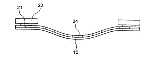
- No suction force acts on the inner periphery. Therefore, when the group of chips 24 is sucked by the Bernoulli chuck 20 and removed from the grinding table, the outer edge of the semiconductor processing adhesive tape 10 is sucked, but the inner circumference is not sucked, and the self-weight of the tape and chips causes the inside of the semiconductor processing adhesive tape 10 to be sucked.
- the circumference hangs down and curves (Fig. 3). As a result, the split chips come into contact with each other, and chipping occurs in which the ends of the chips are damaged.
- the chip spacing (kerf width) is relatively wide, so contact between chips does not occur frequently. Chipping occurs frequently due to contact between chips in contact with each other. In particular, chipping is likely to occur in ultra-thin chips whose bending strength has decreased due to progress in thinning.
- an object of the present invention is to suppress the occurrence of chipping even when a group of chips is conveyed using a Bernoulli chuck.
- the gist of the present invention for the purpose of solving such problems is as follows.
- a pressure-sensitive adhesive tape having a base material, a buffer layer provided on one side of the base material, and an adhesive layer provided on the other side of the base material,
- the semiconductor wafer In the step of grinding the back surface of a semiconductor wafer in which grooves are formed in the surface of the semiconductor wafer or in which a modified region is formed in the semiconductor wafer, and singulating the semiconductor wafer into semiconductor chips by the grinding, the semiconductor wafer
- the semiconductor wafer having the adhesive tape attached to the front surface and having the groove or the modified region formed therein is ground from the back side, and separated into a plurality of chips starting from the groove or the modified region.
- a method of manufacturing a semiconductor device comprising:
- the bending resistance of the tape is controlled within an appropriate range.
- the tape does not warp even when the tape is taped, and the occurrence of chipping can be suppressed.
- FIG. 1 shows a usage mode of a Bernoulli chuck.
- FIG. 3 is a cross-sectional view of FIG. 2;
- Form semiconductor processing means that it can be used in each process such as transportation of semiconductor wafers, back grinding, dicing, and pickup of semiconductor chips.
- the "front surface” of a semiconductor wafer refers to the surface on which circuits are formed, and the “back surface” refers to the surface on which no circuits are formed. Separation of a semiconductor wafer means dividing the semiconductor wafer into individual circuits to obtain semiconductor chips.
- DBG refers to a method in which a groove of a predetermined depth is formed on the front side of the wafer, then the wafer is ground from the back side, and the wafer is singulated by grinding.
- the grooves formed on the surface side of the wafer are formed by a method such as blade dicing, laser dicing or plasma dicing.
- LDBG is a modification of DBG, and refers to a method in which a laser is used to provide a modified region inside the wafer, and the wafer is singulated by stress or the like during grinding of the back surface of the wafer.
- a Bernoulli chuck as shown in FIG. 2, is composed of an arc portion 22 in which a pad 21 is arranged and an arm portion 23 connected to the arc portion.
- the specific configuration thereof is not particularly limited, and various commercially available products can be used.
- the arc may be a closed circular shape (donut shape).
- the so-called Bernoulli effect is used to eject gas toward the chip group to form a negative pressure region, thereby sucking the chips. Therefore, the chip group can be sucked in a non-contact manner.
- the adhesive tape for semiconductor processing according to the present invention may be simply referred to as "adhesive tape".
- the adhesive tape 10 means a laminate including a substrate 11 and an adhesive layer 12, as shown in FIG.
- the adhesive tape 10 has a buffer layer 13 on the surface of the substrate 11 opposite to the adhesive layer 12 .
- a primer layer may be formed on the surface of the substrate on the pressure-sensitive adhesive layer side, and a release sheet may be laminated on the surface of the pressure-sensitive adhesive layer to protect the pressure-sensitive adhesive layer until use.
- the base material may be a single layer or may be a multilayer. The same applies to the adhesive layer and the buffer layer.
- the bending resistance of the laminate of the base material 11 and the buffer layer 13 is 68 mm or more, preferably 69 mm or more.
- the upper limit of the bending resistance is not particularly limited, but if the bending resistance is too high, peeling of the adhesive tape 10 may become difficult. . Since the bending resistance of the laminated body of the base material 11 and the buffer layer 13 included in the semiconductor processing adhesive tape 10 is within the above range, the semiconductor processing adhesive tape 10 holding the chip group is supported by the Bernoulli chuck 20. Even when the adhesive tape 10 is pressed, the adhesive tape 10 is not easily deformed and sagging can be prevented. As a result, contact between chips is reduced, and chipping can be suppressed.
- Bending resistance is measured by the cantilever method.
- the laminate of the base material 11 and the buffer layer 13 was cut into 20 mm width x 150 mm length, and the bending resistance was measured at 23°C and 50% RH using a cantilever type bending resistance tester (manufactured by TOYOSEIKI). Measure (based on JIS L1086). Static electricity affects the measured bending resistance, so static electricity is removed before measurement.
- the laminated body is in roll form, the values in the CD (cross direction) direction are evaluated because the MD (machine direction) direction has large variations.
- the adhesive layer 12 is removed with a solvent or the like. Bending stiffness is measured after removal.
- each member is not particularly limited as long as the bending resistance of the laminate of the base material 11 and the buffer layer 13 is within the above range.
- a preferred configuration of each member of the adhesive tape for semiconductor processing will be described in more detail.
- the Young's modulus of the base material 11 at 23° C. is preferably 1000 MPa or more. If a base material with a Young's modulus of less than 1000 MPa is used, the holding performance of the adhesive tape on the semiconductor wafer or semiconductor chip is reduced, and vibrations, etc. during back grinding cannot be suppressed, resulting in chipping or breakage of the semiconductor chip. easier.
- the inner peripheral portion of the adhesive tape which is not affected by the suction force of the Bernoulli chuck, hangs down and curves.
- the chips on the inner periphery of the adhesive tape may come into contact with each other and chipping may occur.
- the Young's modulus of the base material is set to 1000 MPa or more at 23° C., the performance of holding the semiconductor wafer or semiconductor chip by the adhesive tape is enhanced, suppressing vibration during back grinding, etc., and preventing chipping and breakage of the semiconductor chip. can.
- the Young's modulus of the substrate at 23° C. is more preferably 1800 to 30000 MPa, still more preferably 2500 to 6000 MPa.
- the thickness of the substrate is not particularly limited, it is preferably 80 ⁇ m or less, more preferably 15 to 70 ⁇ m, even more preferably 20 to 60 ⁇ m.
- the thickness of the base material is preferably 80 ⁇ m or less, more preferably 15 to 70 ⁇ m, even more preferably 20 to 60 ⁇ m.
- the material of the substrate is not particularly limited as long as it satisfies the above physical properties, and various resin films can be used.
- a base material having a Young's modulus of 1000 MPa or more at 23° C. for example, polyethylene terephthalate, polyethylene naphthalate, polybutylene terephthalate, polyesters such as wholly aromatic polyesters, polyimides, polyamides, polycarbonates, polyacetals, modified polyphenylene oxides, and polyphenylene sulfides. , polysulfone, polyetherketone, and biaxially oriented polypropylene.
- a film containing one or more selected from a polyester film, a polyamide film, a polyimide film, and a biaxially stretched polypropylene film is preferable, more preferably a polyester film, and further preferably a polyethylene terephthalate film.
- the substrate may contain plasticizers, lubricants, infrared absorbers, ultraviolet absorbers, fillers, colorants, antistatic agents, antioxidants, catalysts, etc., as long as they do not impair the effects of the present invention. good.
- the substrate may be transparent or opaque, and may be colored or vapor-deposited as desired.
- the base material may be subjected to adhesion treatment such as corona treatment in order to improve adhesion with at least one of the buffer layer and the adhesive layer.
- the substrate may have the resin film described above and a primer layer coated on at least one surface of the resin film.
- the primer layer-forming composition for forming the primer layer is not particularly limited, but examples thereof include compositions containing polyester-based resins, urethane-based resins, polyester-urethane-based resins, acrylic-based resins, and the like.
- the primer layer-forming composition may optionally contain a cross-linking agent, a photopolymerization initiator, an antioxidant, a softening agent (plasticizer), a filler, an antirust agent, a pigment, a dye, and the like. .
- the thickness of the primer layer is preferably 0.01-10 ⁇ m, more preferably 0.03-5 ⁇ m.
- the thickness of the primer layer in the examples of the present application is smaller than the thickness of the base material, the thickness of the resin film having the primer layer and the thickness of the base material are substantially the same.
- the material of the primer layer is soft, it has little effect on the Young's modulus, and the Young's modulus of the substrate is substantially the same as that of the resin film even when the primer layer is provided.
- the Young's modulus of the base material can be controlled by selecting the resin composition, adding a plasticizer, and stretching conditions during resin film production. Specifically, when a polyethylene terephthalate film is used as the substrate, the Young's modulus of the substrate tends to decrease as the content of the ethylene component in the copolymer component increases. Moreover, when the amount of the plasticizer blended with respect to the resin composition constituting the base material is increased, the Young's modulus of the base material tends to decrease.
- the pressure-sensitive adhesive layer 12 is not particularly limited as long as it has appropriate pressure-sensitive adhesiveness at room temperature, but preferably has a shear storage modulus of 0.05 to 0.50 MPa at 23°C. Circuits and the like are formed on the surface of a semiconductor wafer, and the surface is usually uneven. By setting the shear storage elastic modulus of the adhesive layer within the above range, when the adhesive tape is applied to the wafer surface having unevenness, the unevenness of the wafer surface and the adhesive layer are sufficiently contacted, and the adhesive layer is smoothed. Adhesiveness can be exhibited appropriately. Therefore, it is possible to reliably fix the adhesive tape to the semiconductor wafer and to appropriately protect the wafer surface during back grinding.
- the shear storage modulus of the adhesive layer is more preferably 0.12 to 0.35 MPa.
- the shear storage elastic modulus of the adhesive layer means the shear storage elastic modulus before curing by energy ray irradiation when the adhesive layer is formed from an energy ray-curable adhesive.
- the shear storage modulus can be measured by the following method.
- a measurement sample is obtained by punching a pressure-sensitive adhesive layer having a thickness of about 0.5 to 1 mm into a circle having a diameter of 7.9 mm.
- the elastic modulus of the measurement sample is measured when the temperature is changed at a temperature increase rate of 3 ° C./min in the temperature range of -30 ° C. to 150 ° C. at a frequency of 1 Hz. .
- the elastic modulus at the measurement temperature of 23°C is taken as the shear storage elastic modulus at 23°C.
- the thickness of the pressure-sensitive adhesive layer is preferably less than 100 ⁇ m, more preferably 5-80 ⁇ m, even more preferably 10-70 ⁇ m.
- the adhesive layer is formed of, for example, an acrylic adhesive, a urethane adhesive, a rubber adhesive, a silicone adhesive, or the like, with the acrylic adhesive being preferred.
- the adhesive layer is preferably formed from an energy ray-curable adhesive.
- an energy ray-curable adhesive for forming the adhesive layer for example, in addition to a non-energy ray-curable adhesive resin (also referred to as “adhesive resin I”), an energy ray-curable compound other than the adhesive resin can be used.
- An energy ray-curable pressure-sensitive adhesive composition (hereinafter also referred to as “X-type pressure-sensitive adhesive composition”) can be used.
- an energy ray-curable adhesive resin hereinafter also referred to as “adhesive resin II" obtained by introducing an unsaturated group into the side chain of a non-energy ray-curable adhesive resin is used.
- a pressure-sensitive adhesive composition (hereinafter, also referred to as "Y-type pressure-sensitive adhesive composition”) containing as a main component and not containing an energy ray-curable compound other than the pressure-sensitive adhesive resin may also be used.
- an energy ray-curable adhesive a combined type of X-type and Y-type, that is, in addition to the energy ray-curable adhesive resin II, an energy ray-curable adhesive containing an energy ray-curable compound other than the adhesive resin is used.
- An adhesive composition hereinafter also referred to as "XY type adhesive composition" may be used.
- the XY-type adhesive composition it is preferable to use the XY-type adhesive composition.
- the XY type it is possible to have sufficient adhesive properties before curing, while sufficiently reducing the peel strength to the semiconductor wafer after curing.
- the adhesive may be formed from a non-energy ray-curable adhesive composition that does not cure even when irradiated with energy rays.
- the non-energy ray-curable adhesive composition contains at least the non-energy ray-curable adhesive resin I, but does not contain the energy ray-curable adhesive resin II and the energy ray-curable compound. be.
- adhesive resin is used as a term indicating one or both of the above-described adhesive resin I and adhesive resin II.
- specific adhesive resins include acrylic resins, urethane resins, rubber resins, and silicone resins, with acrylic resins being preferred.
- the acrylic pressure-sensitive adhesive in which an acrylic resin is used as the pressure-sensitive adhesive resin will be described in more detail below.
- Acrylic polymer is used for acrylic resin.
- the acrylic polymer is obtained by polymerizing a monomer containing at least an alkyl (meth)acrylate, and contains structural units derived from the alkyl (meth)acrylate.
- Alkyl (meth)acrylates include those having 1 to 20 carbon atoms in the alkyl group, and the alkyl group may be linear or branched.
- alkyl (meth)acrylates include methyl (meth)acrylate, ethyl (meth)acrylate, isopropyl (meth)acrylate, n-propyl (meth)acrylate, n-butyl (meth)acrylate, 2-ethylhexyl (meth)acrylate, ) acrylate, n-octyl (meth)acrylate, isooctyl (meth)acrylate, nonyl (meth)acrylate, decyl (meth)acrylate, undecyl (meth)acrylate, dodecyl (meth)acrylate and the like. You may use an alkyl (meth)acrylate individually or in combination of 2 or more types.
- the acrylic polymer preferably contains a structural unit derived from an alkyl (meth)acrylate whose alkyl group has 4 or more carbon atoms.
- the number of carbon atoms in the alkyl (meth)acrylate is preferably 4-12, more preferably 4-6.
- the alkyl (meth)acrylate having an alkyl group having 4 or more carbon atoms is preferably an alkyl acrylate.
- an alkyl group having a carbon number of 4 or more is added in order to adjust the elastic modulus and adhesive properties of the pressure-sensitive adhesive layer.
- a copolymer containing 1 to 3 alkyl (meth)acrylate-derived structural units is preferred.
- the alkyl (meth)acrylate is preferably an alkyl (meth)acrylate having 1 or 2 carbon atoms, more preferably methyl (meth)acrylate, and most preferably methyl methacrylate.
- the content of the alkyl (meth)acrylate having 1 to 3 carbon atoms in the alkyl group is preferably 1 to 30 parts by mass, more preferably 3 to 26 parts by mass, with respect to 100 parts by mass of the total amount of the monomer. parts by mass, more preferably 6 to 22 parts by mass.
- the acrylic polymer preferably has structural units derived from a functional group-containing monomer in addition to the structural units derived from the alkyl (meth)acrylate described above.
- the functional group of the functional group-containing monomer includes a hydroxyl group, a carboxyl group, an amino group, an epoxy group and the like.
- the functional group-containing monomer reacts with a cross-linking agent described later to become a cross-linking starting point, or reacts with an unsaturated group-containing compound to introduce an unsaturated group into the side chain of the acrylic polymer. be.
- Functional group-containing monomers include hydroxyl group-containing monomers, carboxy group-containing monomers, amino group-containing monomers, epoxy group-containing monomers, and the like.
- a hydroxyl group-containing monomer, a carboxy group-containing monomer, an amino group-containing monomer, an epoxy group-containing monomer, and the like may be used alone or in combination of two or more.
- hydroxyl group-containing monomers and carboxy group-containing monomers are preferably used, and hydroxyl group-containing monomers are more preferably used.
- hydroxyl group-containing monomers examples include 2-hydroxyethyl acrylate, 2-hydroxyethyl methacrylate, 2-hydroxypropyl (meth) acrylate, 3-hydroxypropyl (meth) acrylate, 2-hydroxybutyl (meth) acrylate, 3- Hydroxyalkyl (meth)acrylates such as hydroxybutyl (meth)acrylate and 4-hydroxybutyl (meth)acrylate; unsaturated alcohols such as vinyl alcohol and allyl alcohol;
- Carboxy group-containing monomers include, for example, ethylenically unsaturated monocarboxylic acids such as (meth)acrylic acid and crotonic acid; ethylenically unsaturated dicarboxylic acids such as fumaric acid, itaconic acid, maleic acid and citraconic acid, and their anhydrides , 2-carboxyethyl methacrylate and the like.
- monocarboxylic acids such as (meth)acrylic acid and crotonic acid
- dicarboxylic acids such as fumaric acid, itaconic acid, maleic acid and citraconic acid, and their anhydrides
- 2-carboxyethyl methacrylate and the like include, for example, ethylenically unsaturated monocarboxylic acids such as (meth)acrylic acid and crotonic acid; ethylenically unsaturated dicarboxylic acids such as fumaric acid, itaconic acid, maleic acid and citraconic
- the content of the functional group-containing monomer is preferably 1 to 35 parts by mass, more preferably 3 to 32 parts by mass, and still more preferably 6 to 30 parts by mass with respect to 100 parts by mass of the total amount of monomers constituting the acrylic polymer.
- the acrylic polymer may contain structural units derived from monomers copolymerizable with the above acrylic monomers, such as styrene, ⁇ -methylstyrene, vinyl toluene, vinyl formate, vinyl acetate, acrylonitrile, and acrylamide. may contain.
- the above acrylic polymer can be used as a non-energy ray-curable adhesive resin I (acrylic resin).
- the energy ray-curable acrylic resin include those obtained by reacting the functional group of the acrylic polymer I with a compound having a photopolymerizable unsaturated group (also referred to as an unsaturated group-containing compound). .
- the unsaturated group-containing compound is a compound that has both a substituent that can be bonded to the functional group of the acrylic polymer and a photopolymerizable unsaturated group.
- the photopolymerizable unsaturated group includes a (meth)acryloyl group, a vinyl group, an allyl group, a vinylbenzyl group, etc., and a (meth)acryloyl group is preferred.
- an isocyanate group, a glycidyl group, etc. are mentioned as a functional group and a bondable substituent which the unsaturated group containing compound has.
- examples of unsaturated group-containing compounds include (meth)acryloyloxyethyl isocyanate, (meth)acryloylisocyanate, glycidyl (meth)acrylate, and the like.
- the unsaturated group-containing compound preferably reacts with a part of the functional groups of the acrylic polymer.
- 50 to 98 mol% of the functional groups of the acrylic polymer include It is preferable to react the contained compounds, more preferably 55 to 93 mol %.
- the weight average molecular weight (Mw) of the acrylic resin is preferably 300,000 to 1,600,000, more preferably 400,000 to 1,400,000, and still more preferably 500,000 to 1,200,000.
- Energy ray-curable compound contained in the X-type or XY-type pressure-sensitive adhesive composition, a monomer or oligomer having an unsaturated group in the molecule and capable of being polymerized and cured by energy ray irradiation is preferable.
- energy ray-curable compounds include trimethylolpropane tri(meth)acrylate, pentaerythritol (meth)acrylate, pentaerythritol tetra(meth)acrylate, dipentaerythritol hexa(meth)acrylate, 1,4- Polyvalent (meth)acrylate monomers such as butylene glycol di(meth)acrylate, 1,6-hexanediol (meth)acrylate, urethane (meth)acrylate, polyester (meth)acrylate, polyether (meth)acrylate, epoxy ( Oligomers such as meth)acrylates can be mentioned.
- urethane (meth)acrylate oligomers are preferable because they have a relatively high molecular weight and are less likely to reduce the shear storage modulus of the pressure-sensitive adhesive layer.
- the energy ray-curable compound has a molecular weight (weight average molecular weight in the case of an oligomer) of preferably 100 to 12,000, more preferably 200 to 10,000, still more preferably 400 to 8,000, and particularly preferably 600 to 6,000.
- the content of the energy ray-curable compound in the X-type adhesive composition is preferably 40 to 200 parts by mass, more preferably 50 to 150 parts by mass, and still more preferably 60 to 100 parts by mass with respect to 100 parts by mass of the adhesive resin. 90 parts by mass.
- the content of the energy ray-curable compound in the XY-type adhesive composition is preferably 1 to 30 parts by mass, more preferably 2 to 20 parts by mass, and even more preferably 100 parts by mass of the adhesive resin. is 3 to 15 parts by mass.
- the adhesive resin is energy ray-curable, even if the content of the energy ray-curable compound is small, it is possible to sufficiently reduce the peel strength after energy ray irradiation. is.
- the pressure-sensitive adhesive composition preferably further contains a cross-linking agent.
- the cross-linking agent reacts with, for example, a functional group derived from a functional group-containing monomer possessed by the adhesive resin to cross-link the adhesive resins.
- cross-linking agents examples include isocyanate-based cross-linking agents such as tolylene diisocyanate, hexamethylene diisocyanate, and adducts thereof; epoxy-based cross-linking agents such as ethylene glycol glycidyl ether; hexa[1-(2-methyl)-aziridinyl ] aziridine-based cross-linking agents such as triphosphatriazine; chelate-based cross-linking agents such as aluminum chelate; These cross-linking agents may be used alone or in combination of two or more.
- isocyanate-based cross-linking agents are preferable from the viewpoint of increasing cohesive strength and improving adhesive strength, and from the viewpoint of availability.
- the amount of the cross-linking agent is preferably 0.01 to 10 parts by mass, more preferably 0.03 to 7 parts by mass, and still more preferably 0 parts by mass with respect to 100 parts by mass of the adhesive resin. 0.05 to 4 parts by mass.
- the pressure-sensitive adhesive composition when the pressure-sensitive adhesive composition is energy ray-curable, the pressure-sensitive adhesive composition preferably further contains a photopolymerization initiator.
- a photopolymerization initiator By including a photopolymerization initiator, the curing reaction of the pressure-sensitive adhesive composition can sufficiently proceed even with relatively low-energy energy rays such as ultraviolet rays.
- photopolymerization initiators examples include benzoin compounds, acetophenone compounds, acylphosphine oxide compounds, titanocene compounds, thioxanthone compounds, peroxide compounds, and photosensitizers such as amines and quinones.
- photopolymerization initiators may be used alone or in combination of two or more.
- the amount of the photopolymerization initiator is preferably 0.01 to 10 parts by mass, more preferably 0.03 to 5 parts by mass, and still more preferably 0.05 to 5 parts by mass with respect to 100 parts by mass of the adhesive resin. is.
- the pressure-sensitive adhesive composition may contain other additives as long as the effects of the present invention are not impaired.
- Other additives include, for example, antistatic agents, antioxidants, softeners (plasticizers), fillers, rust inhibitors, pigments, dyes, and the like.
- the blending amount of the additives is preferably 0.01 to 6 parts by mass with respect to 100 parts by mass of the adhesive resin.
- the adhesive composition may be further diluted with an organic solvent to form a solution of the adhesive composition, from the viewpoint of improving the applicability to the base material, the buffer layer, and the release sheet.
- organic solvents include methyl ethyl ketone, acetone, ethyl acetate, tetrahydrofuran, dioxane, cyclohexane, n-hexane, toluene, xylene, n-propanol and isopropanol.
- the organic solvents used during the synthesis of the adhesive resin may be used as they are. may be added with one or more organic solvents.
- the buffer layer relieves the stress during grinding of the back surface of the semiconductor wafer and prevents the semiconductor wafer from cracking and chipping.
- the composition of the buffer layer is not limited, but from the viewpoint of easy control of viscoelasticity, it is preferably a cured product of a buffer layer-forming composition containing an energy ray-polymerizable compound.
- a buffer layer-forming composition containing an energy ray-polymerizable compound Each component contained in the layer formed from the buffer layer-forming composition containing the energy ray-polymerizable compound will be described below in order.
- a composition for forming a buffer layer containing an energy ray-polymerizable compound can be cured by being irradiated with an energy ray.
- the composition for forming a buffer layer containing the energy ray-polymerizable compound more specifically contains the urethane (meth)acrylate (a1).
- the composition for forming a buffer layer includes a polymerizable compound (a2) having an alicyclic or heterocyclic group having 6 to 20 ring atoms and/or a polymerizable compound having a functional group. It is more preferable to contain compound (a3).
- the composition for forming a buffer layer may contain a polyfunctional polymerizable compound (a4).
- the composition for forming a buffer layer preferably contains a photopolymerization initiator, and may contain other additives and resin components within a range that does not impair the effects of the present invention.
- a photopolymerization initiator e.g., a photopolymerization initiator
- each component contained in the buffer layer-forming composition containing the energy ray-polymerizable compound will be described in detail below.
- the urethane (meth)acrylate (a1) is a compound having at least a (meth)acryloyl group and a urethane bond, and has the property of being polymerized and cured by energy ray irradiation.
- Urethane (meth)acrylates (a1) are oligomers or polymers.
- the weight average molecular weight (Mw) of component (a1) is preferably 1,000 to 100,000, more preferably 2,000 to 60,000, still more preferably 10,000 to 30,000.
- the number of (meth)acryloyl groups (hereinafter also referred to as "number of functional groups") in component (a1) may be monofunctional, difunctional, or trifunctional or more, but monofunctional or difunctional is preferred. .
- Component (a1) can be obtained, for example, by reacting a terminal isocyanate urethane prepolymer obtained by reacting a polyol compound and a polyvalent isocyanate compound with a (meth)acrylate having a hydroxyl group.
- a component (a1) individually or in combination of 2 or more types.
- the polyol compound used as the raw material for component (a1) is not particularly limited as long as it is a compound having two or more hydroxy groups.
- Specific polyol compounds include, for example, alkylene diols, polyether polyols, polyester polyols, and polycarbonate polyols. Among these, polyester-type polyols and polycarbonate-type polyols are preferred.
- the polyol compound may be a bifunctional diol, a trifunctional triol, or a tetrafunctional or higher polyol, but bifunctional diols are preferred, and polyester diols or polycarbonate diols are more preferred.
- polyvalent isocyanate compounds include aliphatic polyisocyanates such as tetramethylene diisocyanate, hexamethylene diisocyanate and trimethylhexamethylene diisocyanate; Alicyclic diisocyanates such as ,4'-diisocyanate, ⁇ , ⁇ '-diisocyanatedimethylcyclohexane;4,4'-diphenylmethane diisocyanate, tolylene diisocyanate, xylylene diisocyanate, tolidine diisocyanate, tetramethylene xylylene diisocyanate, naphthalene- aromatic diisocyanates such as 1,5-diisocyanate; Among these, isophorone diisocyanate, hexamethylene diisocyanate, and xylylene diisocyanate are preferred.
- a urethane (meth)acrylate (a1) can be obtained by reacting a (meth)acrylate having a hydroxyl group with a terminal isocyanate urethane prepolymer obtained by reacting the above-mentioned polyol compound and a polyvalent isocyanate compound.
- the (meth)acrylate having a hydroxy group is not particularly limited as long as it is a compound having a hydroxy group and a (meth)acryloyl group in at least one molecule.
- Specific (meth)acrylates having a hydroxy group include, for example, 2-hydroxyethyl (meth)acrylate, 2-hydroxypropyl (meth)acrylate, 4-hydroxybutyl (meth)acrylate, 4-hydroxycyclohexyl (meth) Acrylate, 5-hydroxycyclooctyl (meth)acrylate, 2-hydroxy-3-phenyloxypropyl (meth)acrylate, pentaerythritol tri(meth)acrylate, polyethylene glycol mono(meth)acrylate, polypropylene glycol mono(meth)acrylate, etc.
- hydroxyalkyl (meth)acrylate hydroxy group-containing (meth)acrylamide such as N-methylol (meth)acrylamide
- hydroxyalkyl (meth)acrylates are preferred, and 2-hydroxyethyl (meth)acrylate is more preferred.
- the conditions for reacting the isocyanate-terminated urethane prepolymer and the (meth)acrylate having a hydroxy group are preferably conditions for reacting at 60 to 100° C. for 1 to 4 hours in the presence of a solvent and a catalyst added as necessary. .
- Component (a2) is a polymerizable compound having an alicyclic or heterocyclic group having 6 to 20 ring atoms, and more preferably a compound having at least one (meth)acryloyl group. Compounds having one (meth)acryloyl group are preferred.
- component (a2) overlaps with the definition of component (a3) described later, the overlapping part is included in component (a3).
- a compound having at least one (meth)acryloyl group, an alicyclic or heterocyclic group having 6 to 20 ring-forming atoms, and a functional group such as a hydroxyl group, an epoxy group, an amide group, or an amino group is a component
- the compound is included in component (a3).
- the number of ring-forming atoms in the alicyclic group or heterocyclic group of component (a2) is preferably 6 to 20, more preferably 6 to 18, still more preferably 6 to 16, particularly preferably 7 to 12. be.
- Atoms forming the ring structure of the heterocyclic group include, for example, a carbon atom, a nitrogen atom, an oxygen atom, a sulfur atom and the like.
- the number of ring-forming atoms refers to the number of atoms constituting the ring itself of a compound having a structure in which atoms are cyclically bonded, and atoms that do not constitute a ring (for example, hydrogen atoms bonded to atoms that constitute a ring). Also, when the ring is substituted with a substituent, the atoms included in the substituent are not included in the number of ring-forming atoms.
- Examples of specific component (a2) include isobornyl (meth)acrylate, dicyclopentenyl (meth)acrylate, dicyclopentanyl (meth)acrylate, dicyclopentenyloxy (meth)acrylate, cyclohexyl (meth)acrylate, alicyclic group-containing (meth)acrylates such as adamantane (meth)acrylate; heterocyclic group-containing (meth)acrylates such as tetrahydrofurfuryl (meth)acrylate, morpholine (meth)acrylate, and cyclic trimethylolpropane formal acrylate; be done.
- a component (a2) individually or in combination of 2 or more types.
- alicyclic group-containing (meth)acrylates isobornyl (meth)acrylate is preferred.
- the content of the component (a2) in the buffer layer-forming composition is preferably 10 to 80 parts by mass, more preferably 30 to 70 parts by mass, relative to the total amount (100 parts by mass) of the buffer layer-forming composition. is.
- Component (a3) is a polymerizable compound containing a functional group such as a hydroxyl group, an epoxy group, an amide group, or an amino group, and is preferably a compound having at least one (meth)acryloyl group. Compounds having one (meth)acryloyl group are preferred.
- the component (a3) has good compatibility with the component (a1), making it easier to adjust the viscosity of the composition for forming a buffer layer within an appropriate range. Moreover, even if the buffer layer is made relatively thin, the buffer performance is improved.
- component (a3) examples include hydroxyl group-containing (meth)acrylates, epoxy group-containing compounds, amide group-containing compounds, amino group-containing (meth)acrylates, and the like.
- hydroxyl group-containing (meth)acrylates examples include 2-hydroxyethyl (meth)acrylate, 2-hydroxypropyl (meth)acrylate, 3-hydroxypropyl (meth)acrylate, 2-hydroxybutyl (meth)acrylate, 3-hydroxy Butyl (meth)acrylate, 4-hydroxybutyl (meth)acrylate, phenylhydroxypropyl (meth)acrylate, 2-hydroxy-3-phenoxypropyl acrylate and the like.
- epoxy group-containing compounds examples include glycidyl (meth)acrylate, methylglycidyl (meth)acrylate, allyl glycidyl ether, and the like. Among these, epoxy groups such as glycidyl (meth)acrylate and methylglycidyl (meth)acrylate Group-containing (meth)acrylates are preferred.
- amide group-containing compounds include (meth)acrylamide, N,N-dimethyl(meth)acrylamide, N-butyl(meth)acrylamide, N-methylol(meth)acrylamide, N-methylolpropane(meth)acrylamide, N -Methoxymethyl(meth)acrylamide, N-butoxymethyl(meth)acrylamide and the like.
- amino group-containing (meth)acrylates examples include primary amino group-containing (meth)acrylates, secondary amino group-containing (meth)acrylates, and tertiary amino group-containing (meth)acrylates.
- hydroxyl group-containing (meth)acrylates are preferable, and hydroxyl group-containing (meth)acrylates having an aromatic ring such as phenylhydroxypropyl (meth)acrylate are more preferable.
- the content of the component (a3) in the buffer layer-forming composition is preferably 0 to 40 parts by mass, more preferably 0 to 35 parts by mass, relative to the total amount (100 parts by mass) of the buffer layer-forming composition. , more preferably 0 to 30 parts by mass.
- a three-dimensional network structure (crosslinked structure) is formed.
- the number of crosslinked structures formed by energy ray irradiation tends to increase, compared to when a compound containing only one photopolymerizable unsaturated group is used.
- component (a4) overlaps with the definitions of components (a2) and (a3) described above, the overlap is included in component (a4).
- a compound having an alicyclic or heterocyclic group with 6 to 20 ring atoms and two or more (meth)acryloyl groups is included in the definition of both component (a4) and component (a2).
- the compound is included in component (a4).
- compounds containing functional groups such as hydroxyl groups, epoxy groups, amide groups and amino groups and having two or more (meth)acryloyl groups are included in the definition of both component (a4) and component (a3).
- the compound is included in component (a4).
- the number of photopolymerizable unsaturated groups (number of functional groups) in the polyfunctional polymerizable compound is preferably 2-10, more preferably 3-6.
- the weight average molecular weight of component (a4) is preferably 30-40,000, more preferably 100-10,000, and even more preferably 200-1,000.
- Examples of specific component (a4) include ethylene glycol di(meth)acrylate, diethylene glycol di(meth)acrylate, triethylene glycol di(meth)acrylate, tetraethylene glycol di(meth)acrylate, and glycol-derived repeating units.
- Polyethylene glycol di(meth)acrylate generally indicates the number of glycol units in parentheses. For example, when the number of glycol units is 600, it is indicated as polyethylene glycol (600) diacrylate.
- a component (a4) individually or in combination of 2 or more types.
- polyethylene glycol diacrylate and neopentyl glycol di(meth)acrylate are preferred.
- the content of the component (a4) in the buffer layer-forming composition is preferably 2 to 40 parts by mass, more preferably 3 to 20 parts by mass, relative to the total amount (100 parts by mass) of the buffer layer-forming composition. , more preferably 5 to 15 parts by mass.
- composition for forming a buffer layer may contain a polymerizable compound (a5) other than the components (a1) to (a4) as long as the effects of the present invention are not impaired.
- component (a5) examples include alkyl (meth)acrylates having an alkyl group having 1 to 20 carbon atoms; styrene, hydroxyethyl vinyl ether, hydroxybutyl vinyl ether, N-vinylformamide, N-vinylpyrrolidone, N-vinylcaprolactam, and the like. vinyl compound of: and the like.
- the content of the component (a5) in the buffer layer-forming composition is preferably 0 to 20 parts by mass, more preferably 0 to 10 parts by mass, relative to the total amount (100 parts by mass) of the buffer layer-forming composition. , more preferably 0 to 5 parts by mass, particularly preferably 0 to 2 parts by mass.
- the buffer layer-forming composition preferably further contains a photopolymerization initiator from the viewpoint of shortening the polymerization time by light irradiation and reducing the amount of light irradiation when forming the buffer layer.
- photopolymerization initiators examples include benzoin compounds, acetophenone compounds, acylphosphine oxide compounds, titanocene compounds, thioxanthone compounds, peroxide compounds, and photosensitizers such as amines and quinones.
- 1-hydroxycyclohexylphenyl ketone 2-hydroxy-2-methyl-1-phenyl-propan-1-one
- benzoin benzoin methyl ether
- benzoin ethyl ether benzoin isopropyl ether
- benzylphenyl sulfide tetramethylthiuram monosulfide
- azobisisobutyrolnitrile dibenzyl, diacetyl, 8-chloroanthraquinone, bis(2,4,6-trimethylbenzoyl)phenylphosphine oxide and the like.
- photopolymerization initiators can be used alone or in combination of two or more.
- the content of the photopolymerization initiator in the buffer layer-forming composition is preferably 0.05 to 15 parts by mass, more preferably 0.1 to 10 parts by mass, with respect to 100 parts by mass of the total amount of the energy ray-polymerizable compound. parts by mass, more preferably 0.3 to 5 parts by mass.
- the buffer layer-forming composition may contain other additives as long as the effects of the present invention are not impaired.
- Other additives include, for example, antistatic agents, antioxidants, softeners (plasticizers), fillers, rust inhibitors, pigments, dyes, and the like.
- the content of each additive in the buffer layer-forming composition is preferably 0.01 to 6 parts by mass with respect to 100 parts by mass of the total amount of the energy ray-polymerizable compound. More preferably, it is 0.1 to 3 parts by mass.
- the buffer layer-forming composition may contain a resin component as long as the effects of the present invention are not impaired.
- the resin component include polyene/thiol-based resins, polyolefin-based resins such as polybutene, polybutadiene, and polymethylpentene, and thermoplastic resins such as styrene-based copolymers.
- the content of these resin components in the buffer layer-forming composition is preferably 0 to 20 parts by mass, more preferably 0 to 10 parts by mass, relative to the total amount (100 parts by mass) of the buffer layer-forming composition. , more preferably 0 to 5 parts by mass, particularly preferably 0 to 2 parts by mass.
- the buffer layer formed from the buffer layer-forming composition containing the energy ray-polymerizable compound is obtained by polymerizing and curing the buffer layer-forming composition having the above composition by energy ray irradiation. That is, the buffer layer is a cured product of the composition for forming a buffer layer.
- the buffer layer contains polymerized units derived from component (a1). Moreover, the buffer layer preferably contains polymerized units derived from the component (a2) and/or polymerized units derived from the component (a3). Furthermore, polymerized units derived from component (a4) and/or polymerized units derived from component (a5) may be contained.
- the content ratio of each polymer unit in the buffer layer usually corresponds to the ratio (feed ratio) of each component constituting the buffer layer-forming composition. For example, when the content of component (a1) in the buffer layer-forming composition is 10 to 70 parts by mass with respect to the total amount (100 parts by mass) of the buffer layer-forming composition, the buffer layer contains component (a1). It contains 10 to 70 parts by mass of the derived polymerized units.
- the buffer layer-forming composition contains 10 to 80 parts by mass of the derived polymerized units.
- the bending resistance of the laminate of the base material 11 and the buffer layer 13 is 68 mm or more.
- the adhesive tape 10 for semiconductor processing holding a group of chips is supported by the Bernoulli chuck 20, the adhesive tape 10 is not easily deformed and can be prevented from sagging. As a result, contact between chips is reduced, and chipping can be suppressed.
- the bending resistance of the laminate can be controlled by the material and thickness of the base material 11 and the buffer layer 13 . If a film with high rigidity or a thick film is used as the base material, the bending resistance increases. Moreover, even if a film having a dense cross-linked structure or a thick film is used as the buffer layer, the bending resistance increases.
- the buffer layer is obtained by curing the buffer layer-forming composition described above.
- the crosslinked structure of the buffer layer can be adjusted by selecting the composition of the buffer layer-forming composition. Therefore, in order to control the bending resistance of the laminate of the base material and the buffer layer within the above range, the types and amounts of the components constituting the buffer layer-forming composition may be adjusted. Guidelines for adjusting the type and amount of each component are described below. For example, when the urethane (meth)acrylate (a1) has a large number of (meth)acryloyl groups, the crosslinked structure increases in the buffer layer, and the bending resistance of the laminate of the base material and the buffer layer increases.
- the buffer layer contains many crosslinked structures
- the buffer layer becomes hard, and the bending resistance of the laminate of the base material and the buffer layer tends to increase. Therefore, the bending resistance of the laminate can be controlled within an appropriate range by adjusting the amounts of the components involved in the formation of the crosslinked structure.
- components involved in forming a crosslinked structure include (meth)acryloyl groups of urethane (meth)acrylate (a1) and polyfunctional polymerizable compound (a4).
- the polyfunctional polymerizable compound (a4) is easy to use and is a useful component for forming a crosslinked structure.
- the structure of the buffer layer contains a relatively soft structural unit (eg, a unit with a long chain length)
- the bending resistance of the laminate of the base material and the buffer layer tends to decrease. Therefore, the bending resistance of the laminate can be controlled within an appropriate range by adjusting the amount of components involved in the formation of the long chain structure.
- a unit having a long chain length includes a urethane chain of urethane (meth)acrylate (a1).
- the bending resistance is excessively increased, when the semiconductor processing adhesive tape 10 is peeled off from the chip group 24, the repulsive force due to the bending of the tape increases, and excessive pressure is applied to the chips, which may damage the chips. There is That is, if the bending resistance is too high, peeling of the adhesive tape 10 may become difficult, so the bending resistance is preferably 150 mm or less.
- the buffer layer described above contains additives such as plasticizers, lubricants, infrared absorbers, ultraviolet absorbers, fillers, colorants, antistatic agents, antioxidants, and catalysts, as long as they do not impair the effects of the present invention. You may let Moreover, the buffer layer described above may be transparent or opaque, and may be colored or vapor-deposited as desired.
- a release sheet may be attached to the surface of the adhesive tape. Specifically, the release sheet is attached to the surface of the adhesive layer of the adhesive tape. The release sheet is attached to the surface of the adhesive layer to protect the adhesive layer during transportation and storage. The release sheet is releasably attached to the adhesive tape, and is peeled off and removed from the adhesive tape before the adhesive tape is used (that is, before wafer attachment).
- a release sheet having at least one surface subjected to a release treatment is used, and specific examples include a release sheet base material coated with a release agent on the surface thereof.
- a resin film is preferable, and as the resin constituting the resin film, for example, polyester resin films such as polyethylene terephthalate resin, polybutylene terephthalate resin, polyethylene naphthalate resin, polypropylene resin, polyethylene resin, etc. and the like polyolefin resins.
- polyester resin films such as polyethylene terephthalate resin, polybutylene terephthalate resin, polyethylene naphthalate resin, polypropylene resin, polyethylene resin, etc. and the like polyolefin resins.
- release agents include rubber-based elastomers such as silicone-based resins, olefin-based resins, isoprene-based resins and butadiene-based resins, long-chain alkyl-based resins, alkyd-based resins, fluorine-based resins, and the like.
- the thickness of the release sheet is not particularly limited, but is preferably 10-200 ⁇ m, more preferably 20-150 ⁇ m.
- the method for producing the pressure-sensitive adhesive tape of the present invention is not particularly limited, and it can be produced by a known method.
- a method for producing an adhesive tape having a substrate, an adhesive layer provided on one side of the substrate, and a buffer layer provided on the other side of the substrate is as follows. be.
- the buffer layer is formed from a buffer layer-forming composition containing an energy ray-polymerizable compound, a buffer layer provided by coating and curing the buffer layer-forming composition on a release sheet, and a substrate; and removing the release sheet, a laminate of the buffer layer and the substrate is obtained.
- the adhesive layer provided on the release sheet can be attached to the substrate side of the laminate to manufacture an adhesive tape in which the release sheet is attached to the surface of the adhesive layer.
- the release sheet attached to the surface of the pressure-sensitive adhesive layer may be peeled off and removed before use of the pressure-sensitive adhesive tape.
- an adhesive (adhesive composition) is directly applied on a release sheet by a known coating method, and the coating film is dried by heating to form an adhesive layer. Layers can be formed.
- an adhesive may be directly applied to one side of the substrate to form an adhesive layer.
- the method of applying the pressure-sensitive adhesive include the spray coating method, bar coating method, knife coating method, roll coating method, blade coating method, die coating method, gravure coating method, etc. shown in the manufacturing method of the buffer layer.
- the composition for forming the buffer layer is directly applied on the release sheet by a known coating method to form a coating film, and the coating film is irradiated with energy rays.
- a buffer layer can be formed.
- the buffer layer may be formed by directly applying the composition for forming a buffer layer on one side of the base material and drying it by heating or by irradiating the coating film with energy rays.
- Examples of methods for applying the buffer layer-forming composition include spin coating, spray coating, bar coating, knife coating, roll coating, blade coating, die coating, and gravure coating.
- an organic solvent may be added to the composition for forming a buffer layer, and the composition may be applied in the form of a solution onto the release sheet.
- the composition for forming a buffer layer contains an energy ray-polymerizable compound
- the hardening of the buffer layer may be performed in one hardening process, or may be performed in multiple times.
- the coating film on the release sheet may be completely cured to form a buffer layer and then attached to the base material, and a semi-cured buffer layer forming film may be formed without completely curing the coating film. Then, after bonding the buffer layer-forming film to the base material, the energy beam may be irradiated again to completely cure the film, thereby forming the buffer layer.
- Ultraviolet rays are preferable as the energy rays to be irradiated in the curing treatment.
- the coating film of the composition for forming a buffer layer may be exposed, but the coating film is covered with a release sheet or base material, and the energy beam is irradiated in a state where the coating film is not exposed. Curing is preferred.
- the method for producing an adhesive tape having buffer layers on both sides of a base material is, for example, by obtaining a laminate in which a buffer layer, a base material, and a buffer layer are laminated in this order by the method described above, and then A pressure-sensitive adhesive layer may be formed on the buffer layer side.
- the pressure-sensitive adhesive tape according to the present invention is preferably applied to the surface of a semiconductor wafer and used when back-grinding the wafer. More preferably, the pressure-sensitive adhesive tape according to the present invention is preferably used in DBG in which wafer backside grinding and wafer singulation are performed simultaneously. Particularly preferably, the adhesive tape according to the present invention is preferably used for LDBG in which a group of chips with a small kerf width can be obtained when a semiconductor wafer is singulated.
- chip group refers to a plurality of semiconductor chips arranged in a wafer shape and held on the adhesive tape according to the present invention.
- the method for manufacturing a semiconductor device includes at least steps 1 to 5 below.
- Step 1 A step of applying the above adhesive tape to the surface of a semiconductor wafer and cutting the adhesive tape along the outer periphery of the semiconductor wafer
- Step 2 Forming a groove from the front surface side of the semiconductor wafer, or forming a groove on the front surface or the back surface of the semiconductor wafer
- Step 3 The semiconductor wafer with the adhesive tape attached to the surface and the groove or modified region formed is ground from the back side to form the groove or modified region
- Step 4 The adhesive tape for semiconductor processing holding the plurality of singulated chips is supported and conveyed by a Bernoulli chuck
- Step 5 Individual pieces peeling off the adhesive tape from the semiconductor wafer (i.e., a plurality of semiconductor chips)
- Step 1 the adhesive tape of the present invention is attached to the surface of a semiconductor wafer via an adhesive layer, and cut along the outer circumference of the semiconductor wafer.
- the adhesive tape is attached so as to cover the semiconductor wafer and the peripheral table extending around its periphery.
- the adhesive tape is cut by a cutter or the like along the outer periphery of the semiconductor wafer.
- the cutting speed is usually 10-300 mm/s.
- the temperature of the cutter blade during cutting may be room temperature, or the cutting may be performed by heating the cutter blade.
- step 1 may be performed before step 2, which will be described later, or after step 2.
- step 1 is preferably performed before step 2.
- step 1 is performed after step 2.
- the semiconductor wafer used in this manufacturing method may be a silicon wafer, a wafer of gallium arsenide, silicon carbide, lithium tantalate, lithium niobate, gallium nitride, indium phosphide, or the like, or a glass wafer. .
- the thickness of the semiconductor wafer before grinding is not particularly limited, it is usually about 500 to 1000 ⁇ m.
- a semiconductor wafer usually has a circuit formed on its surface. Formation of circuits on the wafer surface can be performed by various methods including conventional methods such as an etching method and a lift-off method.
- the modified region is formed by laser irradiation focused on the inside of the semiconductor wafer, and the modified region is formed inside the semiconductor wafer.
- the laser irradiation may be performed from the front side or the back side of the semiconductor wafer.
- the laser is applied to the semiconductor wafer through the adhesive tape.
- the semiconductor wafer to which the adhesive tape is attached and the grooves or modified regions are formed is placed on the grinding table and held by suction on the grinding table. At this time, the semiconductor wafer is sucked with its surface side arranged on the table side.
- Step 3 After steps 1 and 2, the back surface of the semiconductor wafer on the grinding table is ground to singulate the semiconductor wafer into a plurality of semiconductor chips.
- the back surface grinding is performed so as to thin the semiconductor wafer at least to the position reaching the bottom of the groove.
- the grooves become cuts penetrating the wafer, and the semiconductor wafer is divided by the cuts into individual semiconductor chips.
- the ground surface may reach the modified region by grinding, but it does not have to reach the modified region strictly. That is, the semiconductor wafer may be ground from the modified region to a position close to the modified region so that the semiconductor wafer is broken into individual semiconductor chips starting from the modified region.
- the actual singulation of the semiconductor chips may be performed by applying a pick-up tape, which will be described later, and then stretching the pick-up tape.
- the shape of the individualized semiconductor chips may be a square or an elongated shape such as a rectangle.
- the thickness of the individualized semiconductor chips is not particularly limited, it is preferably about 5 to 100 ⁇ m, more preferably 10 to 45 ⁇ m.
- LDBG a modified region is provided inside the wafer with a laser, and the wafer is singulated by stress or the like during wafer backside grinding. ⁇ 45 ⁇ m becomes easy.
- the size of the individualized semiconductor chips is not particularly limited, but the chip size is preferably less than 600 mm 2 , more preferably less than 400 mm 2 , and even more preferably less than 300 mm 2 .
- the back surface of the chip may be dry-polished. Dry polishing refers to a process of mirror-finishing the rear surface of the individualized chips with a dry grindstone. Through this process, the crushed layer on the back surface of the chip is reduced and the bending strength is increased.
- the bending resistance of the laminate of the base material 11 and the buffer layer 13 is within the above range, so that the adhesive tape 10 for semiconductor processing holding the chip group 24 can be obtained. Even when supported by the Bernoulli chuck 20, the adhesive tape 10 is difficult to deform and can be prevented from sagging. As a result, contact between chips is reduced, and chipping can be suppressed.
- the adhesive layer of the adhesive tape is formed from an energy ray-curable adhesive
- the adhesive layer is cured by irradiation with energy rays.
- a pick-up tape is attached to the rear surface side of the separated semiconductor wafer, and the position and direction are aligned so that pick-up is possible.
- the ring frame arranged on the outer peripheral side of the wafer is also adhered to the pick-up tape, and the outer peripheral edge of the pick-up tape is fixed to the ring frame.
- the wafer and the ring frame may be attached to the pickup tape at the same time, or may be attached at separate timings.
- the adhesive tape is peeled off from the plurality of semiconductor chips held on the pickup tape.
- the adhesive tape 10 has too high rigidity, the repulsive force due to the curvature increases when the adhesive tape is peeled off, and excessive pressure is applied to the chip, which may damage the chip. Therefore, it is preferable to control the bending resistance within an appropriate range.
- the pickup tape is not particularly limited, it is composed of, for example, a base material and an adhesive tape provided with an adhesive layer provided on at least one surface of the base material.
- an adhesive tape can be used instead of the pickup tape.
- the adhesive tape includes a laminate of a film-like adhesive and a release sheet, a laminate of a dicing tape and a film-like adhesive, and an adhesive layer and a release sheet that function as both a dicing tape and a die bonding tape.
- a dicing die bonding tape and the like can be mentioned. That is, the present embodiment may include a step of attaching a dicing die bonding tape to the back surface of the semiconductor wafer.
- a film-like adhesive may be applied to the back side of the semiconductor wafer that has been divided into individual pieces. When a film adhesive is used, the film adhesive may have the same shape as the wafer.
- the plurality of semiconductor chips on the adhesive tape or the pick-up tape is a semiconductor. It is picked up together with the adhesive layer divided into the same shape as the chip. Then, the semiconductor chip is fixed on a substrate or the like via an adhesive layer to manufacture a semiconductor device. The division of the adhesive layer is performed by laser or expansion.
- a protective film forming tape for forming a protective film on the back surface of the chip may be used instead of the adhesive tape.
- the adhesive tape according to the present invention is used in a method for singulating semiconductor wafers by DBG or LDBG. It can be preferably used for LDBG where a chip group having a smaller width and a thinner thickness can be obtained.
- the adhesive tape according to the present invention can also be used for normal back grinding, and can also be used to temporarily hold a workpiece during processing of glass, ceramics, etc. It can also be used. It can also be used as various removable adhesive tapes.
- the bending resistance is adjusted after removing the adhesive layer with a solvent or the like. Measure.
- the wafer was ground (including dry polishing) to a thickness of 30 ⁇ m, and the wafer was singulated into a plurality of chips.
- the diced chips were observed with a digital microscope, and chips with cracks were counted and classified by crack size according to the following criteria. Note that the crack size ( ⁇ m) is obtained by comparing the crack length ( ⁇ m) along the vertical direction of the chip and the crack length ( ⁇ m) along the horizontal direction of the chip, and the larger of the values. and
- a Bernoulli chuck (a circular part with an outer diameter of 300 mm and an inner diameter of 100 mm is provided with 18 pads at approximately equal intervals, and the distance from the outer circumference of the circular part to the center of the pad is 25 mm) is used. Then, the surface of the chip group/adhesive tape on which the chip group is held is sucked without contact, the chip group/adhesive tape is removed from the grinding table of the grinding machine, the number of cracks is measured again, and the number of increased cracks is measured. did.
- a case where all of the following conditions were satisfied was rated as good (A), and a case where even one of the conditions was not satisfied was rated as defective (F).
- the number of large cracks increases less than 1 per wafer (624 chips)
- the number of medium cracks increases less than 10 per wafer (624 chips)
- the number of small cracks increases per wafer (624 chips) less than 30 pieces per
- Example 1 All parts by mass in the following examples and comparative examples are in terms of solid content.
- a PET film with a double-sided coat layer manufactured by Toyobo, product name [Cosmoshine A4300], thickness: 50 ⁇ m, Young's modulus at 23° C.: 2550 MPa was prepared.
- BA N-butyl acrylate
- MMA methyl methacrylate
- 2HEA 2-hydroxyethyl acrylate
- 2HEA 2-hydroxyethyl acrylate
- Buffer layer preparation of composition for forming buffer layer
- Urethane acrylate oligomer (CN8888) purchased from Sartomer, isobornyl acrylate (IBXA), cyclic trimethylolpropane formal acrylate, neopentyl glycol diacrylate, and polyethylene glycol (600) diacrylate were used as energy ray polymerizable compounds.
- 2-Hydroxy-2-methyl-1-phenyl-propan-1-one manufactured by BASF, product name "Omnirad 1173" was added as a photopolymerization initiator. 0 parts by mass were blended to prepare a composition for forming a buffer layer.
- Release sheet manufactured by Lintec, trade name “SP-PET381031” polyethylene terephthalate (PET) film subjected to silicone release treatment, thickness: 38 ⁇ m
- PTT polyethylene terephthalate
- the coating film was semi-cured by irradiating the coating film with ultraviolet rays to form a semi-cured buffer layer with a thickness of 28 ⁇ m.
- the above ultraviolet irradiation is performed using a belt conveyor type ultraviolet irradiation device (product name “ECS-401GX” manufactured by Eyegraphics) and a high-pressure mercury lamp (product name “H04-L41” manufactured by Eyegraphics).
- the measurement was carried out under irradiation conditions of a height of 260 mm, an output of 80 W/cm, an illuminance of 70 mW/cm 2 and an irradiation amount of 30 mW/cm 2 .
- Examples 2 to 4 Comparative Examples 1 and 2> A pressure-sensitive adhesive tape for semiconductor processing was produced in the same manner as in Example 1, except that the composition of the composition for forming a buffer layer was changed as shown in Table 1. Table 1 shows the results.
- the adhesive tape for semiconductor processing according to the present invention since the bending resistance of the tape is controlled within an appropriate range, the adhesive tape for semiconductor processing holding the chip group can be used as a Bernoulli chuck. Even when the tape is conveyed using the tape, there is no bending, and the occurrence of chipping can be suppressed.
Landscapes
- Chemical & Material Sciences (AREA)
- Organic Chemistry (AREA)
- Chemical Kinetics & Catalysis (AREA)
- Adhesives Or Adhesive Processes (AREA)
- Mechanical Treatment Of Semiconductor (AREA)
- Container, Conveyance, Adherence, Positioning, Of Wafer (AREA)
Priority Applications (2)
| Application Number | Priority Date | Filing Date | Title |
|---|---|---|---|
| JP2023510280A JPWO2022209119A1 (https=) | 2021-03-30 | 2022-01-11 | |
| KR1020237026844A KR20230161424A (ko) | 2021-03-30 | 2022-01-11 | 반도체 가공용 점착 테이프 및 반도체 장치의 제조방법 |
Applications Claiming Priority (2)
| Application Number | Priority Date | Filing Date | Title |
|---|---|---|---|
| JP2021057979 | 2021-03-30 | ||
| JP2021-057979 | 2021-03-30 |
Publications (1)
| Publication Number | Publication Date |
|---|---|
| WO2022209119A1 true WO2022209119A1 (ja) | 2022-10-06 |
Family
ID=83455963
Family Applications (1)
| Application Number | Title | Priority Date | Filing Date |
|---|---|---|---|
| PCT/JP2022/000573 Ceased WO2022209119A1 (ja) | 2021-03-30 | 2022-01-11 | 半導体加工用粘着テープおよび半導体装置の製造方法 |
Country Status (4)
| Country | Link |
|---|---|
| JP (1) | JPWO2022209119A1 (https=) |
| KR (1) | KR20230161424A (https=) |
| TW (1) | TW202237777A (https=) |
| WO (1) | WO2022209119A1 (https=) |
Cited By (1)
| Publication number | Priority date | Publication date | Assignee | Title |
|---|---|---|---|---|
| JPWO2024063127A1 (https=) * | 2022-09-22 | 2024-03-28 |
Citations (2)
| Publication number | Priority date | Publication date | Assignee | Title |
|---|---|---|---|---|
| JP2013129723A (ja) * | 2011-12-21 | 2013-07-04 | Lintec Corp | 粘着シートおよび半導体チップの製造方法 |
| WO2013172328A1 (ja) * | 2012-05-14 | 2013-11-21 | リンテック株式会社 | 接着性樹脂層付シートおよび半導体装置の製造方法 |
Family Cites Families (2)
| Publication number | Priority date | Publication date | Assignee | Title |
|---|---|---|---|---|
| JP6322013B2 (ja) | 2014-03-20 | 2018-05-09 | リンテック株式会社 | 粘着シート |
| JP2018100422A (ja) * | 2018-03-20 | 2018-06-28 | リンテック株式会社 | 粘着テープおよび半導体装置の製造方法 |
-
2022
- 2022-01-11 JP JP2023510280A patent/JPWO2022209119A1/ja active Pending
- 2022-01-11 WO PCT/JP2022/000573 patent/WO2022209119A1/ja not_active Ceased
- 2022-01-11 KR KR1020237026844A patent/KR20230161424A/ko active Pending
- 2022-03-28 TW TW111111617A patent/TW202237777A/zh unknown
Patent Citations (2)
| Publication number | Priority date | Publication date | Assignee | Title |
|---|---|---|---|---|
| JP2013129723A (ja) * | 2011-12-21 | 2013-07-04 | Lintec Corp | 粘着シートおよび半導体チップの製造方法 |
| WO2013172328A1 (ja) * | 2012-05-14 | 2013-11-21 | リンテック株式会社 | 接着性樹脂層付シートおよび半導体装置の製造方法 |
Cited By (2)
| Publication number | Priority date | Publication date | Assignee | Title |
|---|---|---|---|---|
| JPWO2024063127A1 (https=) * | 2022-09-22 | 2024-03-28 | ||
| JP7817420B2 (ja) | 2022-09-22 | 2026-02-18 | リンテック株式会社 | 粘着シート、および電子部品または半導体装置の製造方法 |
Also Published As
| Publication number | Publication date |
|---|---|
| KR20230161424A (ko) | 2023-11-27 |
| JPWO2022209119A1 (https=) | 2022-10-06 |
| TW202237777A (zh) | 2022-10-01 |
Similar Documents
| Publication | Publication Date | Title |
|---|---|---|
| JP7207778B2 (ja) | 半導体加工用粘着テープ、及び半導体装置の製造方法 | |
| CN109743881B (zh) | 半导体加工用粘着胶带以及半导体装置的制造方法 | |
| CN112400216B (zh) | 半导体加工用粘着胶带及半导体装置的制造方法 | |
| JP7326270B2 (ja) | 半導体加工用粘着テープおよび半導体装置の製造方法 | |
| KR102642081B1 (ko) | 점착 테이프 및 반도체 장치의 제조 방법 | |
| JP7326248B2 (ja) | 粘着テープおよび半導体装置の製造方法 | |
| JP7741094B2 (ja) | 半導体加工用粘着テープおよび半導体装置の製造方法 | |
| JP7326249B2 (ja) | 粘着テープおよび半導体装置の製造方法 | |
| WO2022201790A1 (ja) | 半導体加工用粘着テープおよび半導体装置の製造方法 | |
| TW201918537A (zh) | 半導體加工用黏著帶以及半導體裝置的製造方法 | |
| WO2022209119A1 (ja) | 半導体加工用粘着テープおよび半導体装置の製造方法 | |
| JP7069116B2 (ja) | バックグラインドテープ用基材 | |
| WO2022209118A1 (ja) | 半導体加工用粘着テープおよび半導体装置の製造方法 | |
| KR20230134093A (ko) | 워크 가공용 보호 시트 및 워크 개편화물의 제조 방법 | |
| TWI913337B (zh) | 半導體加工用黏著帶及半導體裝置的製造方法 | |
| JP7757200B2 (ja) | ワーク加工用保護シートおよびワーク個片化物の製造方法 | |
| JP7850802B2 (ja) | 半導体加工用粘着テープ | |
| WO2022201789A1 (ja) | 半導体加工用粘着テープおよび半導体装置の製造方法 | |
| WO2022201788A1 (ja) | 半導体加工用粘着テープおよび半導体装置の製造方法 | |
| WO2023281859A1 (ja) | 半導体加工用保護シートおよび半導体装置の製造方法 |
Legal Events
| Date | Code | Title | Description |
|---|---|---|---|
| 121 | Ep: the epo has been informed by wipo that ep was designated in this application |
Ref document number: 22779352 Country of ref document: EP Kind code of ref document: A1 |
|
| WWE | Wipo information: entry into national phase |
Ref document number: 2023510280 Country of ref document: JP |
|
| NENP | Non-entry into the national phase |
Ref country code: DE |
|
| 122 | Ep: pct application non-entry in european phase |
Ref document number: 22779352 Country of ref document: EP Kind code of ref document: A1 |