WO2022201874A1 - 撮像装置 - Google Patents
撮像装置 Download PDFInfo
- Publication number
- WO2022201874A1 WO2022201874A1 PCT/JP2022/003761 JP2022003761W WO2022201874A1 WO 2022201874 A1 WO2022201874 A1 WO 2022201874A1 JP 2022003761 W JP2022003761 W JP 2022003761W WO 2022201874 A1 WO2022201874 A1 WO 2022201874A1
- Authority
- WO
- WIPO (PCT)
- Prior art keywords
- charge storage
- changeover switch
- storage unit
- imaging device
- charge
- Prior art date
- Legal status (The legal status is an assumption and is not a legal conclusion. Google has not performed a legal analysis and makes no representation as to the accuracy of the status listed.)
- Ceased
Links
Images




Classifications
-
- H—ELECTRICITY
- H04—ELECTRIC COMMUNICATION TECHNIQUE
- H04N—PICTORIAL COMMUNICATION, e.g. TELEVISION
- H04N25/00—Circuitry of solid-state image sensors [SSIS]; Control thereof
- H04N25/60—Noise processing, e.g. detecting, correcting, reducing or removing noise
- H04N25/62—Detection or reduction of noise due to excess charges produced by the exposure, e.g. smear, blooming, ghost image, crosstalk or leakage between pixels
- H04N25/621—Detection or reduction of noise due to excess charges produced by the exposure, e.g. smear, blooming, ghost image, crosstalk or leakage between pixels for the control of blooming
-
- H—ELECTRICITY
- H04—ELECTRIC COMMUNICATION TECHNIQUE
- H04N—PICTORIAL COMMUNICATION, e.g. TELEVISION
- H04N25/00—Circuitry of solid-state image sensors [SSIS]; Control thereof
- H04N25/70—SSIS architectures; Circuits associated therewith
- H04N25/76—Addressed sensors, e.g. MOS or CMOS sensors
- H04N25/77—Pixel circuitry, e.g. memories, A/D converters, pixel amplifiers, shared circuits or shared components
-
- H—ELECTRICITY
- H04—ELECTRIC COMMUNICATION TECHNIQUE
- H04N—PICTORIAL COMMUNICATION, e.g. TELEVISION
- H04N25/00—Circuitry of solid-state image sensors [SSIS]; Control thereof
- H04N25/40—Extracting pixel data from image sensors by controlling scanning circuits, e.g. by modifying the number of pixels sampled or to be sampled
- H04N25/46—Extracting pixel data from image sensors by controlling scanning circuits, e.g. by modifying the number of pixels sampled or to be sampled by combining or binning pixels
-
- H—ELECTRICITY
- H04—ELECTRIC COMMUNICATION TECHNIQUE
- H04N—PICTORIAL COMMUNICATION, e.g. TELEVISION
- H04N25/00—Circuitry of solid-state image sensors [SSIS]; Control thereof
- H04N25/50—Control of the SSIS exposure
- H04N25/57—Control of the dynamic range
-
- H—ELECTRICITY
- H04—ELECTRIC COMMUNICATION TECHNIQUE
- H04N—PICTORIAL COMMUNICATION, e.g. TELEVISION
- H04N25/00—Circuitry of solid-state image sensors [SSIS]; Control thereof
- H04N25/50—Control of the SSIS exposure
- H04N25/57—Control of the dynamic range
- H04N25/59—Control of the dynamic range by controlling the amount of charge storable in the pixel, e.g. modification of the charge conversion ratio of the floating node capacitance
-
- H—ELECTRICITY
- H04—ELECTRIC COMMUNICATION TECHNIQUE
- H04N—PICTORIAL COMMUNICATION, e.g. TELEVISION
- H04N25/00—Circuitry of solid-state image sensors [SSIS]; Control thereof
- H04N25/70—SSIS architectures; Circuits associated therewith
- H04N25/703—SSIS architectures incorporating pixels for producing signals other than image signals
- H04N25/704—Pixels specially adapted for focusing, e.g. phase difference pixel sets
-
- H—ELECTRICITY
- H04—ELECTRIC COMMUNICATION TECHNIQUE
- H04N—PICTORIAL COMMUNICATION, e.g. TELEVISION
- H04N25/00—Circuitry of solid-state image sensors [SSIS]; Control thereof
- H04N25/70—SSIS architectures; Circuits associated therewith
- H04N25/76—Addressed sensors, e.g. MOS or CMOS sensors
- H04N25/77—Pixel circuitry, e.g. memories, A/D converters, pixel amplifiers, shared circuits or shared components
- H04N25/771—Pixel circuitry, e.g. memories, A/D converters, pixel amplifiers, shared circuits or shared components comprising storage means other than floating diffusion
Definitions
- the present disclosure relates to imaging devices.
- An imaging device generally includes a photoelectric conversion element and a readout circuit (ROIC: Readout Integrated Circuit) that reads electric charges from the photoelectric conversion element.
- the readout circuit is provided with a charge storage unit that stores charges read from the photoelectric conversion element.
- the conversion efficiency which indicates the voltage of the output signal per electron, depends on the capacity of the charge storage section.
- the conversion efficiency is also fixed. In this case, for example, since the conversion efficiency cannot be changed according to the charge amount from the photoelectric conversion element, it is difficult to expand the dynamic range.
- the present disclosure provides an imaging device capable of expanding the dynamic range.
- An imaging device includes a photoelectric conversion element provided in each of a plurality of pixels, a first charge storage unit connected to the photoelectric conversion element, and a first charge storage unit connected in parallel. a second charge storage unit, a reset transistor for resetting the potential of the second charge storage unit, a transfer transistor arranged between the first charge storage unit and the second charge storage unit, and a first charge storage unit a third charge storage unit connected in parallel; a switch;
- the first changeover switch may switch whether to connect the third charge storage unit to the photoelectric conversion element according to the amount of light incident on the photoelectric conversion element.
- the first changeover switch may be turned off when the amount of light is smaller than a reference value, and turned on when the amount of light is larger than the reference value.
- a second changeover switch respectively connected to the reset transistor and the second charge storage unit; a fourth charge storage section disposed between the reset transistor and the second changeover switch or connected in parallel with the second charge storage section via the second changeover switch;
- the second changeover switch may switch whether to connect the fourth charge storage unit to the second charge storage unit in synchronization with the first changeover switch.
- the sum of the capacities of the first charge storage section and the third charge storage section may be equal to the sum of the capacities of the second charge storage section and the fourth charge storage section.
- the reset transistor, the transfer transistor, the first changeover switch, and the second changeover switch may be P-channel MOS transistors.
- the selection transistor may be turned on while the first changeover switch is maintained in the off state, and then the selection transistor may be turned on again after the first changeover switch is switched from the off state to the on state.
- the capacity of the third charge storage section may be larger than the capacity of the first charge storage section.
- an overflow gate transistor for discharging the charge accumulated in the third charge accumulation section may be further provided.
- the reset transistor, the transfer transistor, and the first changeover switch may be P-channel MOS transistors.
- a third changeover switch may be further provided for switching between connecting or not connecting the second charge accumulating portions respectively provided in adjacent pixels adjacent to each other among the plurality of pixels.
- the third changeover switch when the adjacent pixels among the plurality of pixels are added, the third changeover switch is always on, and when the adjacent pixels are not added, the third changeover switch is always off.
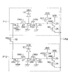
- FIG. 1 is a block diagram showing an example of the configuration of an imaging device according to a first embodiment
- FIG. 2 is a circuit diagram showing the configuration of a pixel according to the first embodiment
- FIG. 4 is a timing chart showing an example of readout operation of the pixel circuit according to the first embodiment
- 4 is a timing chart showing another example of the readout operation of the pixel circuit according to the first embodiment
- FIG. 11 is a circuit diagram showing the configuration of a pixel according to a first modified example
- 9 is a timing chart showing an example of readout operation of the pixel circuit according to the first modified example
- FIG. 11 is a circuit diagram showing the configuration of a pixel according to a second modified example
- FIG. 11 is a timing chart showing an example of readout operation of the pixel circuit according to the second modified example;
- FIG. FIG. 11 is a circuit diagram showing the configuration of a pixel according to a third modified example;
- FIG. 11 is a circuit diagram showing a configuration of a pixel according to a fourth modified example;
- FIG. 11 is a circuit diagram showing a configuration of a pixel according to a fourth modified example;
- FIG. 11 is a circuit diagram showing a configuration of a pixel according to a fourth modified example;
- FIG. 16 is a timing chart showing an example of readout operation of the pixel circuit according to the fourth modified example;
- FIG. FIG. 7 is a circuit diagram showing the configuration of a pixel according to the second embodiment;
- FIG. 7 is a circuit diagram showing the configuration of a pixel according to the second embodiment; 9 is a timing chart showing an example of readout operation of the pixel circuit according to the second embodiment;
- FIG. 12 is a circuit diagram showing the configuration of a pixel according to a fifth modified example;
- FIG. 12 is a circuit diagram showing the configuration of a pixel according to a fifth modified example;
- FIG. 12 is a circuit diagram showing the configuration of a pixel according to a sixth modified example;
- FIG. 12 is a circuit diagram showing the configuration of a pixel according to a sixth modified example;
- FIG. 14 is a circuit diagram showing a configuration of a pixel according to a seventh modified example;
- FIG. 14 is a circuit diagram showing a configuration of a pixel according to a seventh modified example;
- FIG. 14 is a circuit diagram showing a configuration of a pixel according to a seventh modified example;
- FIG. 14 is a circuit diagram showing a configuration of a pixel according to a
- FIG. 12 is a circuit diagram showing the configuration of a pixel according to a sixth modified example;
- FIG. 12 is a circuit diagram showing the configuration of a pixel according to a sixth modified example;
- It is a functional block diagram showing an example of an electronic device.
- 1 is a block diagram showing an example of a schematic configuration of an in-vivo information acquisition system;
- FIG. 1 is a diagram showing an example of a schematic configuration of an endoscopic surgery system;
- FIG. 3 is a block diagram showing an example of functional configurations of a camera head and a CCU;
- FIG. 1 is a block diagram showing an example of a schematic configuration of a vehicle control system;
- FIG. FIG. 4 is an explanatory diagram showing an example of installation positions of an outside information detection unit and an imaging unit;
- FIG. 1 is a block diagram showing an example of the configuration of an imaging device according to the first embodiment.
- the imaging device 1 shown in FIG. 1 is, for example, an infrared image sensor, and has sensitivity to light with a wavelength of 800 nm or more, for example.
- the imaging device 1 is provided with, for example, a rectangular pixel region 10P and an extra-pixel region 10B outside the pixel region 10P.
- a peripheral circuit for driving the pixel region 10P is provided in the non-pixel region 10B.
- a plurality of pixels P are two-dimensionally arranged in the pixel region 10P of the imaging device 1 .
- Peripheral circuits provided in the extra-pixel region 10B include, for example, a row scanning section 201, a horizontal selection section 203, a column scanning section 204, and a system control section 202.
- FIG. 1 A plurality of pixels P are two-dimensionally arranged in the pixel region 10P of the imaging device 1 .
- Peripheral circuits provided in the extra-pixel region 10B include, for example, a row scanning section 201, a horizontal selection section 203, a column scanning section 204, and a system control section 202.
- the row scanning unit 201 is a pixel driving unit configured by shift registers, address decoders, etc., and drives each pixel P, for example, in units of rows.
- a pixel signal output from each pixel P in a pixel row selectively scanned by the row scanning unit 201 is supplied to the horizontal selection unit 203 through each vertical signal line Lsig.
- the horizontal selection unit 203 includes an amplifier, a horizontal selection switch, and the like provided for each vertical signal line Lsig.
- the column scanning unit 204 is composed of a shift register, an address decoder, etc., and sequentially drives the horizontal selection switches of the horizontal selection unit 203 while scanning them. By selective scanning by the column scanning unit 204, the pixel signals of each pixel transmitted through each of the vertical signal lines Lsig are sequentially output to the horizontal signal lines. After that, the pixel signal is input to a signal processing section (not shown) or the like through a horizontal signal line.
- the system control unit 202 receives a clock given from the outside, data instructing an operation mode, etc., and outputs data such as internal information of the imaging device 1 .
- the system control unit 202 further has a timing generator that generates various timing signals, and controls the row scanning unit 201, horizontal selection unit 203, column scanning unit 204, etc. based on the various timing signals generated by the timing generator. Drive control.
- FIG. 2 is a circuit diagram showing the configuration of the pixel P.
- FIG. A pixel P has a photoelectric conversion element 10 and a pixel circuit 20 .
- the photoelectric conversion element 10 is arranged on one semiconductor substrate, and the pixel circuit 20 is arranged on another semiconductor substrate stacked under the one semiconductor substrate.
- the photoelectric conversion element 10 is, for example, a photodiode that photoelectrically converts incident light having a wavelength in the infrared region.
- a photoelectric conversion film (not shown) is provided between an anode electrode and a cathode electrode.
- This photoelectric conversion film is made of, for example, a compound semiconductor material such as a III-V group semiconductor, and photoelectrically converts light with wavelengths from the visible region to the short infrared region.
- Compound semiconductor materials constituting the photoelectric conversion element 10 include, for example, InGaAs (indium gallium arsenide), InAsSb (indium arsenide antimony), GaAsSb (gallium arsenide antimony), InAs (indium arsenide), InSb (indium antimonide), and HgCdTe. (mercury-cadmium-tellurium) or the like can be used.
- the photoelectric conversion film may be made of Ge (germanium).
- the photoelectric conversion film may be made of a semiconductor material having a Type II structure.
- the pixel circuit 20 is an example of a readout circuit that reads out the charge of the photoelectric conversion element 10 .
- the pixel circuit 20 includes a first charge storage unit (SN1) 21, a transfer transistor (TRG) 22, a second charge storage unit (FD1) 23, a reset transistor (RST) 24, and an amplification transistor (AMP) 25. , a selection transistor (SEL) 26 , a switch 27 , and a third charge storage section 28 .
- the first charge storage unit 21 is composed of a capacitor that temporarily holds the charge photoelectrically converted by the photoelectric conversion element 10 .
- One end of the first charge storage unit 21 is connected to the anode electrode of the photoelectric conversion element 10 and the source of the transfer transistor 22 .
- the other end of the first charge storage section 21 is grounded.
- the drain of the transfer transistor 22 is connected to the second charge storage section 23 . That is, the transfer transistor 22 is arranged between the first charge storage section 21 and the second charge storage section 23 .
- the transfer transistor 22 is turned on and off based on a transfer signal input to the gate from the row scanning section 201 . When the transfer transistor 22 is turned on, the charges accumulated in the first charge accumulation section 21 are transferred to the second charge accumulation section 23 via the transfer transistor 22 .
- the second charge storage section 23 is a floating diffusion that stores charges transferred from the first charge storage section 21 .
- One end of the second charge storage unit 23 is connected to the drain of the transfer transistor, the source of the reset transistor 24 and the gate of the amplification transistor 25 .
- the other end of the second charge storage section 23 is grounded.
- the drain of the reset transistor 24 is connected to the power supply VDD.
- the reset transistor 24 is turned on and off based on a reset signal input to its gate from the row scanning section 201 .
- the reset potential VRST is applied to the second charge storage section 23 .
- the reset potential VRST causes the potential of the second charge storage section 23 to be in an initial state (reset state).
- the amplification transistor 25 has a gate connected to the second charge storage unit 23 , a drain connected to the power supply VDD, and a source connected to the drain of the selection transistor 26 .
- the amplification transistor 25 constitutes a load MOS (Metal Oxide Semiconductor) as a constant current source and a source follower circuit connected via a vertical signal line Lsig.
- the amplification transistor 25 generates a pixel signal according to the charge amount accumulated in the second charge accumulation section 23 .
- the source of the selection transistor 26 is connected to the vertical signal line Lsig.
- the selection transistor 26 is turned on and off based on a selection signal input to the gate from the row scanning section 201 .
- the selection transistor 26 is turned on, the pixel signal generated by the amplification transistor 25 is output to the horizontal selection section 203 via the vertical signal line Lsig.
- the changeover switch 27 corresponds to the first changeover switch and is composed of an N-channel MOS transistor.
- the switch 27 has a drain connected to one end of the first charge storage section 21 and a source connected to one end of the third charge storage section 28 . That is, the changeover switch 27 is arranged between the first charge storage section 21 and the third charge storage section 28 .
- the changeover switch 27 is turned on and off based on a control signal input to the gate from the row scanning section 201 . When the changeover switch 27 is turned on, the charges photoelectrically converted by the photoelectric conversion element 10 are accumulated in the third charge accumulation section 28 via the changeover switch 27 .
- the third charge storage unit 28 is composed of a capacitor that temporarily holds the charge photoelectrically converted by the photoelectric conversion element 10 .
- the other end of the third charge storage section 28 is grounded.
- the conversion efficiency changes depending on whether or not the switch 27 connects the third charge storage section 28 to the photoelectric conversion element 10 .
- changeover switch 27 When changeover switch 27 is turned on, conversion efficiency decreases. Conversely, when the changeover switch 27 is turned off, the conversion efficiency increases.
- Equation (1) q is the charge amount of the photoelectric conversion element 10 .
- C sn1 , C sn2 , and C fd1 are the capacitances of the first charge storage section 21, the third charge storage section 28, and the second charge storage section 23, respectively.
- the conversion efficiency (Low) depends on the capacitance of each of the first charge storage section 21, the second charge storage section 23, and the third charge storage section .
- the capacitance Csn2 of the third charge storage section 28 increases, the saturation signal amount also increases. Therefore, it is desirable that the capacitance C sn2 of the third charge storage section 28 is larger than the capacitance C sn1 of the first charge storage section 21 .
- the read noise depends on the balance between the sum of the capacitances C sn1 and C sn2 and the capacitance C fd1 .
- the added value is equal to the capacitance Cfd1 .
- the readout noise is, for example, input conversion random noise (RN) in DDS (Double Delta Sampling) driving, in other words, kT/C noise.
- RN input conversion random noise
- DDS Double Delta Sampling
- FIG. 3 is a timing chart showing an example of the readout operation of the pixel circuit 20.
- the conversion efficiency (Low) is set. Therefore, the changeover switch 27 (SNG) is always on regardless of the D phase (Data Phase) and P phase (Reset Phase).
- the reset transistor 24 (RST), the transfer transistor 22 (TRG), and the select transistor 26 (SEL) are off during the charge accumulation time from time t1 to time t2. Therefore, the charges photoelectrically converted by the photoelectric conversion element 10 are accumulated in the first charge accumulation section 21 and the third charge accumulation section 28 .
- the transfer transistor 22 switches from the off state to the on state within the time from time t2 to time t3.
- the charges accumulated in the first charge accumulation section 21 and the third charge accumulation section 28 are transferred to the second charge accumulation section 23 and amplified as pixel signals by the amplification transistor 25 .
- the selection transistor 26 is turned on. Thereby, the pixel signal is output to the vertical signal line Lsig.
- the selection transistor 26 is turned off during the time from time t3 to time t4. Subsequently, the reset transistor 24, the transfer transistor 22, and the select transistor 26 are simultaneously switched from the off state to the on state. As a result, the charges remaining in the second charge storage section 23 are discharged via the reset transistor 24, so that the second charge storage section 23 is reset to the initial state. After that, the above operation is repeated again.
- the changeover switch 27 (SNG) is always off regardless of the D phase (Data Phase) and P phase (Reset Phase). Further, by adjusting the pulse timing of the signal input to the gate of each transistor, the pixel region 10P can be driven by a global shutter method in which all the pixels P accumulate (expose) charges at the same timing. It is also possible to drive by a rolling shutter method in which each pixel P accumulates charges at different timings.
- FIG. 4 is a timing chart showing another example of the readout operation of the pixel circuit 20.
- FIG. Here, points different from the timing chart shown in FIG. 3 will be described.
- charges set to the conversion efficiency (Hi) and charges set to the conversion efficiency (Low) are read at different times.
- the selection transistor 26 is turned on again after the changeover switch 27 is switched from the off state to the on state, so the charge set to the conversion efficiency (Low) is read.
- the charge set to the conversion efficiency (Hi) and the charge set to the conversion efficiency (Low) can be read out simultaneously in one exposure.
- the dynamic range can be expanded with one exposure.
- the pixel circuit 20 is provided with the changeover switch 27 and the third charge accumulation section 28 . Therefore, by switching ON and OFF of the changeover switch 27 according to the illuminance condition, the capacitance of the entire charge storage section in the pixel circuit 20 changes. Since this also changes the conversion efficiency, it is possible to expand the dynamic range.
- the illuminance conditions may differ for each pixel P within the pixel region 10P. Therefore, in the pixel region 10P, there are pixels P for which the changeover switch 27 is turned on (set to conversion efficiency (Low)) and pixels P for which the changeover switch 27 is turned off (set to conversion efficiency (Hi)). , may be mixed. In this case, the conversion rate can be optimized for each pixel P.
- FIG. 5 is a circuit diagram showing the configuration of a pixel according to the first modified example. Also, FIG. 6 is a timing chart showing an example of the readout operation of the pixel circuit according to the first modification.
- the pixel circuit 20a further includes an overflow gate (OFG) transistor 29 in addition to the components of the pixel circuit 20 described above.
- Overflow gate transistor 29 is composed of an N-channel MOS transistor.
- the overflow gate transistor 29 has a drain connected to the source of the switch 27 and one end of the third charge storage section 28, and a source connected to the power supply VDD.
- the overflow gate transistor 29 is turned on and off based on the discharge signal input to the gate from the row scanning section 201 .
- the overflow gate transistor 29 changes from the off state to the Switch to ON state.
- the charges remaining in the third charge storage section 28 are discharged to the power supply VDD via the overflow gate transistor 29 .
- the pixel circuit 20a has the overflow gate transistor 29, so that the charge remaining in the third charge storage section 28 can be discharged. Thereby, blooming to other pixels P can be suppressed.
- FIG. 7 is a circuit diagram showing the configuration of a pixel according to the second modification. Also, FIG. 8 is a timing chart showing an example of the readout operation of the pixel circuit according to the second modification.
- the transfer transistor 22, the reset transistor 24, and the changeover switch 27 are all composed of N-channel MOS transistors.
- the transfer transistor 22, the reset transistor 24, and the changeover switch 27 are all composed of P-channel MOS transistors.
- the conductivity types of the transfer transistor 22, the reset transistor 24, and the changeover switch 27 are opposite to those in the first embodiment. Therefore, in this modification, as shown in FIG. 8, the signal level input to the gate of each transistor is opposite to that in the first embodiment.
- the transfer transistor 22, the reset transistor 24, and the switch 27 are all composed of P-channel MOS transistors. Therefore, the readout of the signal charge from the photoelectric conversion element 10 is the readout of the hole, which is the positive charge. In this case, charges are less likely to overflow from the first charge storage section 21, the second charge storage section 23, and the third charge storage section 28 compared to the case where these transistors are N-channel MOS transistors. Therefore, this modification can also suppress blooming between pixels P adjacent to each other.
- FIG. 9 is a circuit diagram showing the configuration of a pixel according to the third modification.
- a pixel circuit 20c shown in FIG. 9 is further provided with the overflow gate transistor 29 described in the first modification in addition to the components of the pixel circuit 20b in the second modification described above.
- the overflow gate transistor 29 is composed of a P-channel MOS transistor.
- a pixel circuit 20c according to this modified example has a configuration in which the first modified example and the second modified example are combined. Therefore, the charge remaining in the third charge storage section 28 can be discharged by the overflow gate transistor 29, and the charge is transferred to the first charge storage section 21 and the second charge storage section 21 by forming the pixel transistor with a P-channel MOS transistor. It becomes difficult for the charge to overflow from the storage section 23 and the third charge storage section 28 .
- FIG. 10A, 10B, and 10C are circuit diagrams showing pixel configurations according to the fourth modification. Also, FIG. 11 is a timing chart showing an example of the readout operation of the pixel circuit according to the fourth modification.
- a changeover switch 30 is arranged between the pixel P11 and the pixel P12.
- the pixel P11 and the pixel P12 are commonly connected to the vertical signal line Lsig and are adjacent to each other.
- the changeover switch 30 corresponds to a third changeover switch and is composed of an N-channel MOS transistor.
- the drain of the changeover switch 30 is connected to the second charge storage section 23 of the pixel P11, and the source is connected to the second charge storage section 23 of the pixel P12.
- the changeover switch 30 is turned on and off based on a signal input to the gate from the row scanning section 201 .
- the changeover switch 30 (FDX) is always on during the period from time t1 to time t4 (within the period of the D phase and the P phase)
- the second charge storage unit 23 is shared between the pixel P11 and the pixel P12, and the charge accumulated in the second charge accumulation section 23 is thereby added.
- the sensitivity and saturation signal amount are doubled.
- the change-over switch 30 is always off during the above time, the second charge storage units 23 are not shared, so the charges stored in the respective second charge storage units 23 are not added.
- the changeover switch 30 is arranged between the first charge storage section 21 of the pixel P11 and the first charge storage section 21 of the pixel P12.
- the switch 30 When the switch 30 is always on, the first charge storage section 21 of the pixel P11 is connected via the switch 30 to the first charge storage section 21 of the pixel P12.
- the first charge accumulating portion 21 is shared between the pixel P11 and the pixel P12, and the charges accumulated in the first charge accumulating portion 21 are thereby added.
- the amount of signal saturation is doubled.
- the change-over switch 30 is always off during the above time, the first charge storage units 21 are not shared, so the charges stored in the respective first charge storage units 21 are not added.
- the changeover switch 30 is arranged between the third charge storage section 28 of the pixel P11 and the third charge storage section 28 of the pixel P12.
- the changeover switch 30 is always on, the third charge storage section 28 of the pixel P11 is connected via the changeover switch 30 to the third charge storage section 28 of the pixel P12.
- the third charge accumulation section 28 is shared between the pixel P11 and the pixel P12, and the charges accumulated in the third charge accumulation section 28 are added.
- the change-over switch 30 is always off during the above time, the third charge storage units 28 are not shared, so the charges stored in the respective third charge storage units 28 are not added.
- the changeover switch 30 connects the first charge storage unit 21, the second charge storage unit 23, or the third charge storage unit 28 arranged in pixels adjacent to each other is determined. can be switched. Thereby, the sensitivity and saturation signal amount can be adjusted.
- the changeover switch 30 is arranged between pixels adjacent in a direction (vertical direction) parallel to the vertical signal line Lsig. may be arranged between the pixels to be used.
- (Second embodiment) 12A and 12B are circuit diagrams showing configurations of pixels according to the second embodiment. Components similar to those of the first embodiment described above are denoted by the same reference numerals, and detailed description thereof is omitted.
- a pixel circuit 20d shown in FIG. 12A and a pixel circuit 20e shown in FIG. 12B further have a changeover switch 31 and a fourth charge accumulation section 32 in addition to the components of the pixel circuit 20 described in the first embodiment.
- the changeover switch 31 corresponds to a second changeover switch and is composed of an N-channel MOS transistor.
- the fourth charge storage unit 32 is configured with a capacitor.
- the switch 31 has the drain connected to the source of the reset transistor 24 and the source connected to the second charge storage section 23 .
- the changeover switch 31 is turned on and off based on a signal input to the gate from the row scanning section 201 .
- One end of the fourth charge storage section 32 is connected to the source of the reset transistor 24 and the drain of the switch 31, and the other end is grounded.
- a source is connected to one end of the fourth charge storage unit 32 .
- the other end of the fourth charge storage section 32 is grounded. That is, the fourth charge storage section 32 is connected to the second charge storage section 23 via the switch 31 .
- the changeover switch 27 switches whether or not the third charge storage unit 28 is connected to the photoelectric conversion element 10, and the changeover switch 31 switches the fourth charge storage unit.
- the conversion efficiency changes by switching whether or not the section 32 is connected to the second charge storage section 23 .
- changeover switch 27 is turned on, conversion efficiency decreases. Conversely, when the changeover switch 27 is turned off, the conversion efficiency increases.
- Equation (2) C fd2 is the capacitance of the fourth charge storage section 32 .
- the conversion efficiency (Low) depends on the capacity of each of the first charge storage section 21, the second charge storage section 23, the third charge storage section 28, and the fourth charge storage section 32. .
- the capacitance C fd2 of the fourth charge storage unit 32 increases, the saturation signal amount also increases. Therefore, the capacitance C fd2 of the fourth charge storage section 32 is preferably larger than the capacitance C fd1 of the second charge storage section 23 .
- the read noise depends on the balance between the first added value of the capacitances C sn1 and C sn2 and the second added value of the capacitances C fd1 and C fd2 .
- the first addition value be equal to the second addition value.
- readout noise can be reduced by turning off the switch 27 and the switch 31 at low illuminance when the amount of light incident on the photoelectric conversion element 10 is smaller than the reference value.
- the saturation signal amount can be increased by turning on the switch 27 and the switch 31 .
- FIG. 13 is a timing chart showing an example of readout operations of the pixel circuits 20d and 20e according to the second embodiment.
- the conversion efficiency (Low) is set.
- the changeover switch 27 (SNG) not only the changeover switch 27 (SNG) but also the changeover switch 31 (FDG) are always on regardless of the D phase and P phase.
- the changeover switches 27 and 31 are always off regardless of the D phase and P phase.
- the changeover switch 31 operates in synchronization with the changeover switch 27 .
- the reset transistor 24, the transfer transistor 22, and the selection transistor 26 may be driven according to the timing chart shown in FIG. 11, as in the first embodiment.
- the charges set to the conversion efficiency (Hi) and the charges set to the conversion efficiency (Low) can be simultaneously read out by one exposure.
- the dynamic range can be expanded with one exposure.
- the conversion efficiency can be switched by controlling the ON and OFF of the changeover switch 31 in addition to the changeover switch 27 . Furthermore, by adjusting the balance between the SN capacities of the first charge accumulating section 21 and the third charge accumulating section 28 and the FD capacities of the second charge accumulating section 23 and the fourth charge accumulating section 32, Imaging at a high SN ratio becomes possible.
- 14A and 14B are circuit diagrams showing the pixel configuration according to the fifth modification.
- a pixel circuit 20f shown in FIG. 14A and a pixel circuit 20g shown in FIG. 14B further include an overflow gate transistor 29, as in the first modification described above.
- the overflow gate transistor 29 is driven according to the timing chart shown in FIG. 6, as in the first modified example. That is, during the time from time t2 to time t3, the overflow gate transistor 29 switches from the off state to the on state during the period from when the selection transistor 26 is turned off until the selection transistor 26 is turned on. As a result, the charges remaining in the third charge storage section 28 are discharged to the power supply VDD via the overflow gate transistor 29 .
- the conversion efficiency (Hi) is set, the change-over switch 31 and the change-over switch 27 are always in an off state, and when the conversion efficiency (Low) is set, the change-over switch 31 and the change-over switch 27 Always on.
- the pixel circuits 20f and 20g have the overflow gate transistors 29, so that the charges remaining in the third charge storage section 28 can be discharged. Thereby, blooming to other pixels P can be suppressed.
- (Sixth modification) 15A and 15B are circuit diagrams showing pixel configurations according to the sixth modification. Comparing the pixel circuit 20h shown in FIG. 15A with the pixel circuit 20d shown in FIG. 12A, the transfer transistor 22, the reset transistor 24, the changeover switch 27, and the changeover switch 31 are all P-channel transistors instead of N-channel MOS transistors. MOS transistors.
- the conductivity types of the transfer transistor 22, reset transistor 24, changeover switch 27, and changeover switch 31 are opposite to those in the second embodiment. Therefore, in this modification, the signal level input to the gate of each transistor is opposite to that in the second embodiment.
- the transfer transistor 22, the reset transistor 24, the changeover switch 27, and the changeover switch 31 are all composed of P-channel MOS transistors. Therefore, the readout of the signal charge from the photoelectric conversion element 10 is the readout of the hole, which is the positive charge. Therefore, electric charges are less likely to overflow from the first charge storage portion 21 , the second charge storage portion 23 , the third charge storage portion 28 , and the fourth charge storage portion 32 . Therefore, this modification can also suppress blooming between adjacent pixels.
- (Seventh modification) 16A and 16B are circuit diagrams showing pixel configurations according to the seventh modification.
- the transfer transistor 22, the reset transistor 24, the changeover switch 27, the changeover switch 31, and the overflow gate transistor 29 are all N-channel MOS transistors. Instead, it is composed of a P-channel MOS transistor.
- a pixel circuit 20k according to this modified example has a configuration in which the fifth modified example and the sixth modified example are combined. Therefore, the charge remaining in the third charge storage section 28 can be discharged by the overflow gate transistor 29, and the charge is transferred to the first charge storage section 21 and the second charge storage section 21 by forming the pixel transistor with a P-channel MOS transistor. It becomes difficult for the charge to overflow from the storage section 23 and the third charge storage section 28 .
- FIG. 17A and 17B are circuit diagrams showing pixel configurations according to the eighth modification.
- the changeover switch 30 is arranged between the pixel P21 and the pixel P22, as in the above-described fourth modified example.
- the pixel P21 and the pixel P22 are commonly connected to the vertical signal line Lsig and are adjacent to each other.
- each of pixel P21 and pixel P22 has a pixel circuit 20d shown in FIG. 12A.
- each of the pixels P21 and P22 has the pixel circuit 20e shown in FIG. 12B.
- the drain of the changeover switch 30 is connected between the second charge accumulation section 23 of the pixel P21 and the changeover switch 31, and the source is connected between the second charge accumulation section 23 of the pixel P22 and the changeover switch 31. ing.
- the changeover switch 31 is always on during the D-phase and P-phase periods. Conversely, if the charge is not added, the switch 31 is always off during the D-phase and P-phase periods.
- connection form of the changeover switch 30 is not limited to the arrangement shown in FIGS. 17A and 17B.
- the changeover switch 30 may switch the connection between the second charge storage units 21 as in FIG. 10B, or may switch the connection between the third charge storage units 28 as in FIG. 10C.
- the changeover switch 30 connects the first charge storage unit 21, the second charge storage unit 23, or the third charge storage unit 28 arranged in pixels adjacent to each other is determined. can be switched. Thereby, the sensitivity and saturation signal amount can be adjusted.
- the changeover switch 30 is arranged between the pixels adjacent in the direction parallel to the vertical signal line Lsig, but is arranged between the pixels adjacent in the direction orthogonal to the vertical signal line Lsig. good too.
- FIG. 18 shows a schematic configuration of an electronic device 3 (camera) as an example.
- the electronic device 3 is, for example, a camera capable of capturing still images or moving images, and includes an imaging device 1, an optical system 310, a shutter device 311, a driving unit 313 that drives the imaging device 1 and the shutter device 311, a signal and a processing unit 312 .
- the optical system 310 guides image light (incident light) from the subject to the imaging device 1 .
- This optical system 310 may be composed of a plurality of optical lenses.
- the shutter device 311 controls a light irradiation period and a light shielding period for the imaging device 1 .
- the drive unit 313 controls the transfer operation of the imaging device 1 and the shutter operation of the shutter device 311 .
- the signal processing unit 312 performs various signal processing on the signal output from the imaging device 1 .
- the video signal Dout after signal processing is stored in a storage medium such as a memory, or output to a monitor or the like.
- the technology (this technology) according to the present disclosure can be applied to various products.
- the technology according to the present disclosure may be applied to an endoscopic surgery system.
- FIG. 19 is a block diagram showing an example of a schematic configuration of a system for acquiring in-vivo information of a patient using a capsule endoscope, to which the technology according to the present disclosure (this technology) can be applied.
- the in-vivo information acquisition system 10001 is composed of a capsule endoscope 10100 and an external control device 10200.
- the capsule endoscope 10100 is swallowed by the patient during examination.
- the capsule endoscope 10100 has an imaging function and a wireless communication function, and moves inside organs such as the stomach and intestines by peristaltic motion or the like until it is naturally expelled from the patient.
- Images (hereinafter also referred to as in-vivo images) are sequentially captured at predetermined intervals, and information about the in-vivo images is sequentially wirelessly transmitted to the external control device 10200 outside the body.
- the external control device 10200 comprehensively controls the operation of the in-vivo information acquisition system 10001 .
- the external control device 10200 receives information about the in-vivo image transmitted from the capsule endoscope 10100, and displays the in-vivo image on a display device (not shown) based on the received information about the in-vivo image.
- the in-vivo information acquisition system 10001 can obtain in-vivo images of the patient's insides at any time during the period from when the capsule endoscope 10100 is swallowed to when the capsule endoscope 10100 is expelled.
- a capsule endoscope 10100 has a capsule-shaped housing 10101, and the housing 10101 contains a light source unit 10111, an imaging unit 10112, an image processing unit 10113, a wireless communication unit 10114, a power supply unit 10115, and a power supply unit. 10116 and a control unit 10117 are housed.
- the light source unit 10111 is composed of a light source such as an LED (light emitting diode), for example, and irradiates the imaging field of the imaging unit 10112 with light.
- a light source such as an LED (light emitting diode)
- the imaging unit 10112 is composed of an imaging element and an optical system including a plurality of lenses provided in front of the imaging element. Reflected light (hereinafter referred to as observation light) of the light applied to the body tissue to be observed is condensed by the optical system and enters the imaging device. In the imaging unit 10112, the imaging element photoelectrically converts the observation light incident thereon to generate an image signal corresponding to the observation light. An image signal generated by the imaging unit 10112 is provided to the image processing unit 10113 .
- the image processing unit 10113 is composed of a processor such as a CPU (Central Processing Unit) or a GPU (Graphics Processing Unit), and performs various signal processing on the image signal generated by the imaging unit 10112.
- the image processing unit 10113 provides the signal-processed image signal to the wireless communication unit 10114 as RAW data.
- the wireless communication unit 10114 performs predetermined processing such as modulation processing on the image signal processed by the image processing unit 10113, and transmits the image signal to the external control device 10200 via the antenna 10114A. Also, the wireless communication unit 10114 receives a control signal regarding drive control of the capsule endoscope 10100 from the external control device 10200 via the antenna 10114A. Wireless communication section 10114 provides control signal received from external control device 10200 to control section 10117 .
- the power supply unit 10115 is composed of an antenna coil for power reception, a power regeneration circuit that regenerates power from the current generated in the antenna coil, a booster circuit, and the like. Power supply unit 10115 generates electric power using the principle of so-called contactless charging.
- the power supply unit 10116 is composed of a secondary battery and stores the power generated by the power supply unit 10115 .
- FIG. 19 to avoid complication of the drawing, illustration of arrows and the like indicating the destination of power supply from the power supply unit 10116 is omitted.
- the imaging unit 10112, the image processing unit 10113, the wireless communication unit 10114, and the control unit 10117 can be used to drive these units.
- the control unit 10117 is configured by a processor such as a CPU, and controls the driving of the light source unit 10111, the imaging unit 10112, the image processing unit 10113, the wireless communication unit 10114, and the power supply unit 10115 in response to control signals transmitted from the external control device 10200. Control accordingly.
- a processor such as a CPU
- the external control device 10200 is composed of a processor such as a CPU or GPU, or a microcomputer or control board in which a processor and storage elements such as memory are mounted together.
- the external control device 10200 controls the operation of the capsule endoscope 10100 by transmitting a control signal to the controller 10117 of the capsule endoscope 10100 via the antenna 10200A.
- a control signal from the external control device 10200 can change the irradiation condition of the light source unit 10111 for the observation target.
- the control signal from the external control device 10200 can change the imaging conditions (for example, frame rate, exposure value, etc. in the imaging unit 10112).
- the content of processing in the image processing unit 10113 and the conditions for transmitting image signals by the wireless communication unit 10114 may be changed by a control signal from the external control device 10200. .
- the external control device 10200 performs various image processing on the image signal transmitted from the capsule endoscope 10100, and generates image data for displaying the captured in-vivo image on the display device.
- the image processing includes, for example, development processing (demosaicing processing), image quality improvement processing (band enhancement processing, super-resolution processing, NR (noise reduction) processing and/or camera shake correction processing, etc.), and/or enlargement processing ( Various signal processing such as electronic zoom processing) can be performed.
- the external control device 10200 controls driving of the display device to display an in-vivo image captured based on the generated image data.
- the external control device 10200 may cause the generated image data to be recorded in a recording device (not shown) or printed out by a printing device (not shown).
- the technology (the present technology) according to the present disclosure can be applied to various products.
- the technology according to the present disclosure may be applied to an endoscopic surgery system.
- FIG. 20 is a diagram showing an example of a schematic configuration of an endoscopic surgery system to which the technology according to the present disclosure (this technology) can be applied.
- FIG. 20 shows an operator (doctor) 11131 performing surgery on a patient 11132 on a patient bed 11133 using an endoscopic surgery system 11000 .
- an endoscopic surgery system 11000 includes an endoscope 11100, other surgical instruments 11110 such as a pneumoperitoneum tube 11111 and an energy treatment instrument 11112, and a support arm device 11120 for supporting the endoscope 11100. , and a cart 11200 loaded with various devices for endoscopic surgery.
- An endoscope 11100 is composed of a lens barrel 11101 whose distal end is inserted into the body cavity of a patient 11132 and a camera head 11102 connected to the proximal end of the lens barrel 11101 .
- an endoscope 11100 configured as a so-called rigid scope having a rigid lens barrel 11101 is illustrated, but the endoscope 11100 may be configured as a so-called flexible scope having a flexible lens barrel. good.
- the tip of the lens barrel 11101 is provided with an opening into which the objective lens is fitted.
- a light source device 11203 is connected to the endoscope 11100, and light generated by the light source device 11203 is guided to the tip of the lens barrel 11101 by a light guide extending inside the lens barrel 11101, where it reaches the objective. Through the lens, the light is irradiated toward the observation object inside the body cavity of the patient 11132 .
- the endoscope 11100 may be a straight scope, a perspective scope, or a side scope.
- An optical system and an imaging element are provided inside the camera head 11102, and the reflected light (observation light) from the observation target is focused on the imaging element by the optical system.
- the imaging device photoelectrically converts the observation light to generate an electrical signal corresponding to the observation light, that is, an image signal corresponding to the observation image.
- the image signal is transmitted to a camera control unit (CCU: Camera Control Unit) 11201 as RAW data.
- CCU Camera Control Unit
- the CCU 11201 is composed of a CPU (Central Processing Unit), a GPU (Graphics Processing Unit), etc., and controls the operations of the endoscope 11100 and the display device 11202 in an integrated manner. Further, the CCU 11201 receives an image signal from the camera head 11102 and performs various image processing such as development processing (demosaicing) for displaying an image based on the image signal.
- CPU Central Processing Unit
- GPU Graphics Processing Unit
- the display device 11202 displays an image based on an image signal subjected to image processing by the CCU 11201 under the control of the CCU 11201 .
- the light source device 11203 is composed of a light source such as an LED (light emitting diode), for example, and supplies the endoscope 11100 with irradiation light for imaging a surgical site or the like.
- a light source such as an LED (light emitting diode)
- LED light emitting diode
- the input device 11204 is an input interface for the endoscopic surgery system 11000.
- the user can input various information and instructions to the endoscopic surgery system 11000 via the input device 11204 .
- the user inputs an instruction or the like to change the imaging conditions (type of irradiation light, magnification, focal length, etc.) by the endoscope 11100 .
- the treatment instrument control device 11205 controls driving of the energy treatment instrument 11112 for tissue cauterization, incision, blood vessel sealing, or the like.
- the pneumoperitoneum device 11206 inflates the body cavity of the patient 11132 for the purpose of securing the visual field of the endoscope 11100 and securing the operator's working space, and injects gas into the body cavity through the pneumoperitoneum tube 11111. send in.
- the recorder 11207 is a device capable of recording various types of information regarding surgery.
- the printer 11208 is a device capable of printing various types of information regarding surgery in various formats such as text, images, and graphs.
- the light source device 11203 that supplies the endoscope 11100 with irradiation light for photographing the surgical site can be composed of, for example, a white light source composed of an LED, a laser light source, or a combination thereof.
- a white light source is configured by a combination of RGB laser light sources
- the output intensity and output timing of each color (each wavelength) can be controlled with high accuracy. It can be carried out.
- the observation target is irradiated with laser light from each of the RGB laser light sources in a time-division manner, and by controlling the drive of the imaging element of the camera head 11102 in synchronization with the irradiation timing, each of RGB can be handled. It is also possible to pick up images by time division. According to this method, a color image can be obtained without providing a color filter in the imaging element.
- the driving of the light source device 11203 may be controlled so as to change the intensity of the output light every predetermined time.
- the drive of the imaging device of the camera head 11102 in synchronism with the timing of the change in the intensity of the light to obtain an image in a time-division manner and synthesizing the images, a high dynamic A range of images can be generated.
- the light source device 11203 may be configured to be able to supply light in a predetermined wavelength band corresponding to special light observation.
- special light observation for example, the wavelength dependence of light absorption in body tissues is used to irradiate a narrower band of light than the irradiation light (i.e., white light) used during normal observation, thereby observing the mucosal surface layer.
- irradiation light i.e., white light
- Narrow Band Imaging in which a predetermined tissue such as a blood vessel is imaged with high contrast, is performed.
- fluorescence observation may be performed in which an image is obtained from fluorescence generated by irradiation with excitation light.
- the body tissue is irradiated with excitation light and the fluorescence from the body tissue is observed (autofluorescence observation), or a reagent such as indocyanine green (ICG) is locally injected into the body tissue and the body tissue is A fluorescence image can be obtained by irradiating excitation light corresponding to the fluorescence wavelength of the reagent.
- the light source device 11203 can be configured to be able to supply narrowband light and/or excitation light corresponding to such special light observation.
- FIG. 21 is a block diagram showing an example of functional configurations of the camera head 11102 and CCU 11201 shown in FIG.
- the camera head 11102 has a lens unit 11401, an imaging section 11402, a drive section 11403, a communication section 11404, and a camera head control section 11405.
- the CCU 11201 has a communication section 11411 , an image processing section 11412 and a control section 11413 .
- the camera head 11102 and the CCU 11201 are communicably connected to each other via a transmission cable 11400 .
- a lens unit 11401 is an optical system provided at a connection with the lens barrel 11101 . Observation light captured from the tip of the lens barrel 11101 is guided to the camera head 11102 and enters the lens unit 11401 .
- a lens unit 11401 is configured by combining a plurality of lenses including a zoom lens and a focus lens.
- the number of imaging elements constituting the imaging unit 11402 may be one (so-called single-plate type) or plural (so-called multi-plate type).
- image signals corresponding to RGB may be generated by each image pickup element, and a color image may be obtained by synthesizing the image signals.
- the imaging unit 11402 may be configured to have a pair of imaging elements for respectively acquiring right-eye and left-eye image signals corresponding to 3D (dimensional) display.
- the 3D display enables the operator 11131 to more accurately grasp the depth of the living tissue in the surgical site.
- a plurality of systems of lens units 11401 may be provided corresponding to each imaging element.
- the imaging unit 11402 does not necessarily have to be provided in the camera head 11102 .
- the imaging unit 11402 may be provided inside the lens barrel 11101 immediately after the objective lens.
- the drive unit 11403 is configured by an actuator, and moves the zoom lens and focus lens of the lens unit 11401 by a predetermined distance along the optical axis under control from the camera head control unit 11405 . Thereby, the magnification and focus of the image captured by the imaging unit 11402 can be appropriately adjusted.
- the communication unit 11404 is composed of a communication device for transmitting and receiving various information to and from the CCU 11201.
- the communication unit 11404 transmits the image signal obtained from the imaging unit 11402 as RAW data to the CCU 11201 via the transmission cable 11400 .
- the communication unit 11404 receives a control signal for controlling driving of the camera head 11102 from the CCU 11201 and supplies it to the camera head control unit 11405 .
- the control signal includes, for example, information to specify the frame rate of the captured image, information to specify the exposure value at the time of imaging, and/or information to specify the magnification and focus of the captured image. Contains information about conditions.
- the imaging conditions such as the frame rate, exposure value, magnification, and focus may be appropriately designated by the user, or may be automatically set by the control unit 11413 of the CCU 11201 based on the acquired image signal. good.
- the endoscope 11100 is equipped with so-called AE (Auto Exposure) function, AF (Auto Focus) function, and AWB (Auto White Balance) function.
- the camera head control unit 11405 controls driving of the camera head 11102 based on the control signal from the CCU 11201 received via the communication unit 11404.
- the communication unit 11411 is composed of a communication device for transmitting and receiving various information to and from the camera head 11102 .
- the communication unit 11411 receives image signals transmitted from the camera head 11102 via the transmission cable 11400 .
- the communication unit 11411 transmits a control signal for controlling driving of the camera head 11102 to the camera head 11102 .
- Image signals and control signals can be transmitted by electric communication, optical communication, or the like.
- the image processing unit 11412 performs various types of image processing on the image signal, which is RAW data transmitted from the camera head 11102 .
- the control unit 11413 performs various controls related to imaging of the surgical site and the like by the endoscope 11100 and display of the captured image obtained by imaging the surgical site and the like. For example, the control unit 11413 generates control signals for controlling driving of the camera head 11102 .
- control unit 11413 causes the display device 11202 to display a captured image showing the surgical site and the like based on the image signal that has undergone image processing by the image processing unit 11412 .
- the control unit 11413 may recognize various objects in the captured image using various image recognition techniques. For example, the control unit 11413 detects the shape, color, and the like of the edges of objects included in the captured image, thereby detecting surgical instruments such as forceps, specific body parts, bleeding, mist during use of the energy treatment instrument 11112, and the like. can recognize.
- the control unit 11413 may use the recognition result to display various types of surgical assistance information superimposed on the image of the surgical site. By superimposing and presenting the surgery support information to the operator 11131, the burden on the operator 11131 can be reduced and the operator 11131 can proceed with the surgery reliably.
- a transmission cable 11400 connecting the camera head 11102 and the CCU 11201 is an electrical signal cable compatible with electrical signal communication, an optical fiber compatible with optical communication, or a composite cable of these.
- wired communication is performed using the transmission cable 11400, but communication between the camera head 11102 and the CCU 11201 may be performed wirelessly.
- the technology according to the present disclosure may also be applied to, for example, a microsurgery system.
- the technology according to the present disclosure may be realized as a device mounted on any type of moving object such as automobiles, electric vehicles, hybrid electric vehicles, motorcycles, bicycles, personal mobility, airplanes, drones, ships, and robots. good.
- FIG. 22 is a block diagram showing a schematic configuration example of a vehicle control system, which is an example of a mobile control system to which the technology according to the present disclosure can be applied.
- a vehicle control system 12000 includes a plurality of electronic control units connected via a communication network 12001.
- vehicle control system 12000 includes drive system control unit 12010 , body system control unit 12020 , vehicle exterior information detection unit 12030 , vehicle interior information detection unit 12040 , and integrated control unit 12050 .
- a microcomputer 12051 , an audio/image output unit 12052 , and an in-vehicle network I/F (Interface) 12053 are also illustrated as the functional configuration of the integrated control unit 12050 .
- the drive system control unit 12010 controls the operation of devices related to the drive system of the vehicle according to various programs.
- the driving system control unit 12010 includes a driving force generator for generating driving force of the vehicle such as an internal combustion engine or a driving motor, a driving force transmission mechanism for transmitting the driving force to the wheels, and a steering angle of the vehicle. It functions as a control device such as a steering mechanism to adjust and a brake device to generate braking force of the vehicle.
- the body system control unit 12020 controls the operation of various devices equipped on the vehicle body according to various programs.
- the body system control unit 12020 functions as a keyless entry system, a smart key system, a power window device, or a control device for various lamps such as headlamps, back lamps, brake lamps, winkers or fog lamps.
- the body system control unit 12020 can receive radio waves transmitted from a portable device that substitutes for a key or signals from various switches.
- the body system control unit 12020 receives the input of these radio waves or signals and controls the door lock device, power window device, lamps, etc. of the vehicle.
- the vehicle exterior information detection unit 12030 detects information outside the vehicle in which the vehicle control system 12000 is installed.
- the vehicle exterior information detection unit 12030 is connected with an imaging section 12031 .
- the vehicle exterior information detection unit 12030 causes the imaging unit 12031 to capture an image of the exterior of the vehicle, and receives the captured image.
- the vehicle exterior information detection unit 12030 may perform object detection processing or distance detection processing such as people, vehicles, obstacles, signs, or characters on the road surface based on the received image.
- the imaging unit 12031 is an optical sensor that receives light and outputs an electrical signal according to the amount of received light.
- the imaging unit 12031 can output the electric signal as an image, and can also output it as distance measurement information.
- the light received by the imaging unit 12031 may be visible light or non-visible light such as infrared rays.
- the in-vehicle information detection unit 12040 detects in-vehicle information.
- the in-vehicle information detection unit 12040 is connected to, for example, a driver state detection section 12041 that detects the state of the driver.
- the driver state detection unit 12041 includes, for example, a camera that captures an image of the driver, and the in-vehicle information detection unit 12040 detects the degree of fatigue or concentration of the driver based on the detection information input from the driver state detection unit 12041. It may be calculated, or it may be determined whether the driver is dozing off.
- the microcomputer 12051 calculates control target values for the driving force generator, the steering mechanism, or the braking device based on the information inside and outside the vehicle acquired by the vehicle exterior information detection unit 12030 or the vehicle interior information detection unit 12040, and controls the drive system control unit.
- a control command can be output to 12010 .
- the microcomputer 12051 realizes the functions of ADAS (Advanced Driver Assistance System) including collision avoidance or shock mitigation of vehicles, follow-up driving based on inter-vehicle distance, vehicle speed maintenance driving, vehicle collision warning, vehicle lane deviation warning, etc. Cooperative control can be performed for the purpose of ADAS (Advanced Driver Assistance System) including collision avoidance or shock mitigation of vehicles, follow-up driving based on inter-vehicle distance, vehicle speed maintenance driving, vehicle collision warning, vehicle lane deviation warning, etc. Cooperative control can be performed for the purpose of ADAS (Advanced Driver Assistance System) including collision avoidance or shock mitigation of vehicles, follow-up driving based on inter-vehicle distance, vehicle speed maintenance driving
- the microcomputer 12051 controls the driving force generator, the steering mechanism, the braking device, etc. based on the information about the vehicle surroundings acquired by the vehicle exterior information detection unit 12030 or the vehicle interior information detection unit 12040, so that the driver's Cooperative control can be performed for the purpose of autonomous driving, etc., in which vehicles autonomously travel without depending on operation.
- the microcomputer 12051 can output a control command to the body system control unit 12030 based on the information outside the vehicle acquired by the information detection unit 12030 outside the vehicle.
- the microcomputer 12051 controls the headlamps according to the position of the preceding vehicle or the oncoming vehicle detected by the vehicle exterior information detection unit 12030, and performs cooperative control aimed at anti-glare such as switching from high beam to low beam. It can be carried out.
- the audio/image output unit 12052 transmits at least one of audio and/or image output signals to an output device capable of visually or audibly notifying the passengers of the vehicle or the outside of the vehicle.
- an audio speaker 12061, a display section 12062 and an instrument panel 12063 are illustrated as output devices.
- the display unit 12062 may include at least one of an on-board display and a head-up display, for example.
- FIG. 23 is a diagram showing an example of the installation position of the imaging unit 12031.
- the imaging unit 12031 has imaging units 12101, 12102, 12103, 12104, and 12105.
- the imaging units 12101, 12102, 12103, 12104, and 12105 are provided at positions such as the front nose, side mirrors, rear bumper, back door, and windshield of the vehicle 12100, for example.
- An image pickup unit 12101 provided in the front nose and an image pickup unit 12105 provided above the windshield in the passenger compartment mainly acquire images in front of the vehicle 12100 .
- Imaging units 12102 and 12103 provided in the side mirrors mainly acquire side images of the vehicle 12100 .
- An imaging unit 12104 provided in the rear bumper or back door mainly acquires an image behind the vehicle 12100 .
- the imaging unit 12105 provided above the windshield in the passenger compartment is mainly used for detecting preceding vehicles, pedestrians, obstacles, traffic lights, traffic signs, lanes, and the like.
- FIG. 23 shows an example of the imaging range of the imaging units 12101 to 12104.
- the imaging range 12111 indicates the imaging range of the imaging unit 12101 provided in the front nose
- the imaging range 1211212113 indicates the imaging ranges of the imaging units 12102 and 12103 provided in the side mirrors
- the imaging range 12114 indicates the imaging range of the rear bumper or
- the imaging range of the imaging unit 12104 provided in the back door is shown.
- a bird's-eye view image of the vehicle 12100 viewed from above can be obtained.
- At least one of the imaging units 12101 to 12104 may have a function of acquiring distance information.
- at least one of the imaging units 12101 to 12104 may be a stereo camera composed of a plurality of imaging elements, or may be an imaging element having pixels for phase difference detection.
- the microcomputer 12051 determines the distance to each three-dimensional object within the imaging ranges 12111 to 12114 and changes in this distance over time (relative velocity with respect to the vehicle 12100). , it is possible to extract, as the preceding vehicle, the closest three-dimensional object on the traveling path of the vehicle 12100, which runs at a predetermined speed (for example, 0 km/h or more) in substantially the same direction as the vehicle 12100. can. Furthermore, the microcomputer 12051 can set the inter-vehicle distance to be secured in advance in front of the preceding vehicle, and perform automatic brake control (including following stop control) and automatic acceleration control (including following start control). In this way, cooperative control can be performed for the purpose of automatic driving in which the vehicle autonomously travels without depending on the operation of the driver.
- automatic brake control including following stop control
- automatic acceleration control including following start control
- the microcomputer 12051 converts three-dimensional object data related to three-dimensional objects to other three-dimensional objects such as motorcycles, ordinary vehicles, large vehicles, pedestrians, and utility poles. It can be classified and extracted and used for automatic avoidance of obstacles. For example, microcomputer 12051 distinguishes obstacles around vehicle 12100 into obstacles visible to the driver of vehicle 12100 and obstacles difficult to see. Then, the microcomputer 12051 judges the collision risk indicating the degree of danger of collision with each obstacle, and when the collision risk is equal to or higher than the set value and there is a possibility of collision, the obstacle is detected through the audio speaker 12061 and the display unit 12062. By outputting an alarm to the driver via the drive system control unit 12010 and performing forced deceleration and avoidance steering via the drive system control unit 12010, driving assistance for collision avoidance can be performed.
- At least one of the imaging units 12101 to 12104 may be an infrared camera that detects infrared rays.
- the microcomputer 12051 can recognize a pedestrian by determining whether or not the pedestrian exists in the captured images of the imaging units 12101 to 12104 .
- recognition of a pedestrian is performed by, for example, a procedure for extracting feature points in images captured by the imaging units 12101 to 12104 as infrared cameras, and performing pattern matching processing on a series of feature points indicating the outline of an object to determine whether or not the pedestrian is a pedestrian.
- the audio image output unit 12052 outputs a rectangular outline for emphasis to the recognized pedestrian. is superimposed on the display unit 12062 . Also, the audio/image output unit 12052 may control the display unit 12062 to display an icon or the like indicating a pedestrian at a desired position.
- the technology according to the present disclosure can be applied, for example, to the imaging unit 12031 among the configurations described above.
- the imaging device 1 can be applied to the imaging unit 12031 .
- the dynamic range of the imaging unit 12031 is expanded.
- this technique can take the following structures.
- An imaging device comprising: (2) The imaging device according to (1), wherein the first changeover switch switches whether to connect the third charge storage unit to the photoelectric conversion element according to the amount of light incident on the photoelectric conversion element.
- the imaging device according to any one of (4) to (6), wherein the reset transistor, the transfer transistor, the first switch, and the second switch are P-channel MOS transistors.
- (8) further comprising a selection transistor for switching whether to output a pixel signal corresponding to the amount of charge accumulated in the second charge accumulation unit; From (1), the selection transistor is turned on while the first changeover switch is maintained in the off state, and then the selection transistor is turned on again after the first changeover switch is switched from the off state to the on state.
- the imaging device according to any one of the above.
- the imaging device according to any one of (1) to (8), wherein the capacity of the third charge storage section is larger than the capacity of the first charge storage section. (10) Among the plurality of pixels, a pixel in which the third charge storage unit is connected to the photoelectric conversion element by the first changeover switch, and a pixel in which the third charge storage unit is connected to the photoelectric conversion element by the first changeover switch.
- the imaging device according to any one of (1) to (9), in which pixels that are not connected to conversion elements are mixed.
- the imaging device according to any one of (1) to (10), further comprising an overflow gate transistor that discharges charges accumulated in the third charge accumulation section.
- the imaging device according to any one of (1) to 10, wherein the reset transistor, the transfer transistor, and the first switch are P-channel MOS transistors. (13) Further comprising a third changeover switch for switching whether or not to connect the second charge accumulation portions respectively provided in adjacent pixels among the plurality of pixels, (1) to (10) The imaging device according to any one of 1. (14) When the adjacent pixels among the plurality of pixels are added, the third changeover switch is always on, and when the adjacent pixels are not added, the third changeover switch is always off. The imaging device according to (13), which is in a state.
- Imaging Device 10 Photoelectric Conversion Element 21: First Charge Storage Section 22: Transfer Transistor 23: Second Charge Storage Section 24: Reset Transistor 26: Selection Transistor 27: Changeover Switch 28: Third Charge Storage Section 29: Overflow Gate Transistor 30: Changeover switch 31: Changeover switch 32: Fourth charge storage unit
Landscapes
- Engineering & Computer Science (AREA)
- Multimedia (AREA)
- Signal Processing (AREA)
- Transforming Light Signals Into Electric Signals (AREA)
- Solid State Image Pick-Up Elements (AREA)
Abstract
Description
前記リセットトランジスタと前記第2切り替えスイッチとの間に配置されるか、またはた前記第2切り替えスイッチを介して前記第2電荷蓄積部と並列に接続された第4電荷蓄積部と、をさらに備えていてもよい。
前記第1切り替えスイッチがオフ状態に維持されて前記選択トランジスタがオンし、続いて前記第1切り替えスイッチが前記オフ状態からオン状態に切り替わった後、前記選択トランジスタが再びオンしてもよい。
図1は、第1実施形態に係る撮像装置の構成の一例を示すブロック図である。図1に示す撮像装置1は、例えば赤外線イメージセンサであり、例えば波長800nm以上の光に対しても感度を有する。この撮像装置1には、例えば矩形状の画素領域10Pと、画素領域10Pの外側の画素外領域10Bとが設けられている。画素外領域10Bには、画素領域10Pを駆動するための周辺回路が設けられている。

以下、第1実施形態のいくつかの変形例を説明する。上述した第1実施形態と同様の構成要素には、同じ符号を付し、詳細な説明を省略する。
図7は、第2変形例に係る画素の構成を示す回路図である。また、図8は、第2変形例に係る画素回路の読み出し動作の一例を示すタイミングチャートである。
図9は、第3変形例に係る画素の構成を示す回路図である。図9に示す画素回路20cには、上述した第2変形例の画素回路20bの構成要素に加えて、第1変形例で説明したオーバーフローゲートトランジスタ29がさらに設けられている。ただし、本変形例では、オーバーフローゲートトランジスタ29は、Pチャネル型MOSトランジスタで構成される。
図10A、図10B、および図10Cは、第4変形例に係る画素の構成を示す回路図である。また、図11は、第4変形例に係る画素回路の読み出し動作の一例を示すタイミングチャートである。
図12Aおよび図12Bは、第2実施形態に係る画素の構成を示す回路図である。上述した第1実施形態と同様の構成要素には、同じ符号を付し、詳細な説明を省略する。

以下、第2実施形態のいくつかの変形例を説明する。上述した第2実施形態と同様の構成要素には、同じ符号を付し、詳細な説明を省略する。
図15Aおよび図15Bは、第6変形例に係る画素の構成を示す回路図である。図15Aに示す画素回路20hを、図12Aに示す画素回路20dと対比すると、転送トランジスタ22、リセットトランジスタ24、切り替えスイッチ27、および切り替えスイッチ31の全てが、Nチャネル型MOSトランジスタの代わりにPチャネル型MOSトランジスタで構成されている。
図16Aおよび図16Bは、第7変形例に係る画素の構成を示す回路図である。図16Aに示す画素回路20jを図14Aに示す画素回路20fと対比すると、転送トランジスタ22、リセットトランジスタ24、切り替えスイッチ27、切り替えスイッチ31、およびオーバーフローゲートトランジスタ29の全てが、Nチャネル型MOSトランジスタの代わりにPチャネル型MOSトランジスタで構成されている。
図17Aおよび図17Bは、第8変形例に係る画素の構成を示す回路図である。本変形例では、上述した第4変形例と同様に、切り替えスイッチ30が画素P21と画素P22との間に配置されている。画素P21および画素P22は、垂直信号線Lsigに共通に接続され、互いに隣接している。
上述した撮像装置1は、赤外領域を撮像可能なカメラの他に、様々なタイプの電子機器に適用することができる。図18に、その一例として、電子機器3(カメラ)の概略構成を示す。この電子機器3は、例えば静止画または動画を撮影可能なカメラであり、撮像装置1と、光学系310と、シャッタ装置311と、撮像装置1およびシャッタ装置311を駆動する駆動部313と、信号処理部312と、を備える。
更に、本開示に係る技術(本技術)は、様々な製品へ応用することができる。例えば、本開示に係る技術は、内視鏡手術システムに適用されてもよい。
本開示に係る技術(本技術)は、様々な製品へ応用することができる。例えば、本開示に係る技術は、内視鏡手術システムに適用されてもよい。
本開示に係る技術は、自動車、電気自動車、ハイブリッド電気自動車、自動二輪車、自転車、パーソナルモビリティ、飛行機、ドローン、船舶、ロボット等のいずれかの種類の移動体に搭載される装置として実現されてもよい。
(1) 複数の画素の各々に設けられた光電変換素子と、
前記光電変換素子に接続された第1電荷蓄積部と、
前記第1電荷蓄積部と並列に接続された第2電荷蓄積部と、
前記第2電荷蓄積部の電位をリセットするリセットトランジスタと、
前記第1電荷蓄積部と前記第2電荷蓄積部との間に配置された転送トランジスタと、
前記第1電荷蓄積部と並列に接続された第3電荷蓄積部と、
前記第1電荷蓄積部と前記第3電荷蓄積部との間に配置され、前記第3電荷蓄積部を前記光電変換素子に接続するか否かを切り替える第1切り替えスイッチと、
を備える、撮像装置。
(2) 第1切り替えスイッチが、前記光電変換素子への入射光の光量に応じて前記第3電荷蓄積部を前記光電変換素子に接続するか否かを切り替える、(1)に記載の撮像装置。
(3) 第1切り替えスイッチは、前記光量が基準値よりも小さい場合にオフ状態となり、前記光量が前記基準値よりも大きい場合にオン状態となる、(2)に記載の撮像装置。
(4) 前記リセットトランジスタおよび前記第2電荷蓄積部にそれぞれ接続された第2切り替えスイッチと、
前記リセットトランジスタと前記第2切り替えスイッチとの間に配置されるか、またはた前記第2切り替えスイッチを介して前記第2電荷蓄積部と並列に接続された第4電荷蓄積部と、をさらに備える、(1)から(3)のいずれかに記載の撮像装置。
(5) 前記第2切り替えスイッチは、前記第1切り替えスイッチと同期して前記第4電荷蓄積部を前記第2電荷蓄積部に接続するか否かを切り替える、(4)に記載の撮像装置。
(6) 前記第1電荷蓄積部および前記第3電荷蓄積部の容量の加算値が、前記第2電荷蓄積部および前記第4電荷蓄積部の容量の加算値に等しい、(4)または(5)に記載の撮像装置。
(7) 前記リセットトランジスタ、前記転送トランジスタ、前記第1切り替えスイッチ、および前記第2切り替えスイッチが、Pチャネル型MOSトランジスタである、(4)から(6)のいずれかに記載の撮像装置。
(8) 前記第2電荷蓄積部に蓄積された電荷量に応じた画素信号を出力するか否かを切り替える選択トランジスタをさらに備え、
前記第1切り替えスイッチがオフ状態に維持されて前記選択トランジスタがオンし、続いて前記第1切り替えスイッチが前記オフ状態からオン状態に切り替わった後、前記選択トランジスタが再びオンする、(1)から(7)のいずれかに記載の撮像装置。
(9) 前記第3電荷蓄積部の容量が、前記第1電荷蓄積部の容量よりも大きい、(1)から(8)のいずれかに記載の撮像装置。
(10) 前記複数の画素の中で、前記第1切り替えスイッチによって前記第3電荷蓄積部が前記光電変換素子に接続される画素と、前記第1切り替えスイッチによって前記第3電荷蓄積部が前記光電変換素子に接続されない画素と、が混在する、(1)から(9)のいずれかに記載の撮像装置。
(11) 前記第3電荷蓄積部に蓄積された電荷を排出するオーバーフローゲートトランジスタをさらに備える、(1)から(10)のいずれかに記載の撮像装置。
(12) 前記リセットトランジスタ、前記転送トランジスタ、および第1切り替えスイッチが、Pチャネル型MOSトランジスタである、(1)から10のいずれかに記載の撮像装置。
(13) 前記複数の画素の中で互いに隣接する隣接画素にそれぞれ設けられた前記第2電荷蓄積部同士を接続するか否かを切り替える第3切り替えスイッチをさらに備える、(1)から(10)のいずれかに記載の撮像装置。
(14) 前記複数の画素の中で、前記隣接画素を加算する場合には前記第3切り替えスイッチは常時オン状態であり、前記隣接画素を加算しない場合には前記前記第3切り替えスイッチは常時オフ状態である、(13)に記載の撮像装置。
10:光電変換素子
21:第1電荷蓄積部
22:転送トランジスタ
23:第2電荷蓄積部
24:リセットトランジスタ
26:選択トランジスタ
27:切り替えスイッチ
28:第3電荷蓄積部
29:オーバーフローゲートトランジスタ
30:切り替えスイッチ
31:切り替えスイッチ
32:第4電荷蓄積部
Claims (14)
- 複数の画素の各々に設けられた光電変換素子と、
前記光電変換素子に接続された第1電荷蓄積部と、
前記第1電荷蓄積部と並列に接続された第2電荷蓄積部と、
前記第2電荷蓄積部の電位をリセットするリセットトランジスタと、
前記第1電荷蓄積部と前記第2電荷蓄積部との間に配置された転送トランジスタと、
前記第1電荷蓄積部と並列に接続された第3電荷蓄積部と、
前記第1電荷蓄積部と前記第3電荷蓄積部との間に配置され、前記第3電荷蓄積部を前記光電変換素子に接続するか否かを切り替える第1切り替えスイッチと、
を備える、撮像装置。 - 第1切り替えスイッチが、前記光電変換素子への入射光の光量に応じて前記第3電荷蓄積部を前記光電変換素子に接続するか否かを切り替える、請求項1に記載の撮像装置。
- 第1切り替えスイッチは、前記光量が基準値よりも小さい場合にオフ状態となり、前記光量が前記基準値よりも大きい場合にオン状態となる、請求項2に記載の撮像装置。
- 前記リセットトランジスタおよび前記第2電荷蓄積部にそれぞれ接続された第2切り替えスイッチと、
前記リセットトランジスタと前記第2切り替えスイッチとの間に配置されるか、またはた前記第2切り替えスイッチを介して前記第2電荷蓄積部と並列に接続された第4電荷蓄積部と、をさらに備える、請求項1に記載の撮像装置。 - 前記第2切り替えスイッチは、前記第1切り替えスイッチと同期して前記第4電荷蓄積部を前記第2電荷蓄積部に接続するか否かを切り替える、請求項4に記載の撮像装置。
- 前記第1電荷蓄積部および前記第3電荷蓄積部の容量の加算値が、前記第2電荷蓄積部および前記第4電荷蓄積部の容量の加算値に等しい、請求項4に記載の撮像装置。
- 前記リセットトランジスタ、前記転送トランジスタ、前記第1切り替えスイッチ、および前記第2切り替えスイッチが、Pチャネル型MOSトランジスタである、請求項4に記載の撮像装置。
- 前記第2電荷蓄積部に蓄積された電荷量に応じた画素信号を出力するか否かを切り替える選択トランジスタをさらに備え、
前記第1切り替えスイッチがオフ状態に維持されて前記選択トランジスタがオンし、続いて前記第1切り替えスイッチが前記オフ状態からオン状態に切り替わった後、前記選択トランジスタが再びオンする、請求項1に記載の撮像装置。 - 前記第3電荷蓄積部の容量が、前記第1電荷蓄積部の容量よりも大きい、請求項1に記載の撮像装置。
- 前記複数の画素の中で、前記第1切り替えスイッチによって前記第3電荷蓄積部が前記光電変換素子に接続される画素と、前記第1切り替えスイッチによって前記第3電荷蓄積部が前記光電変換素子に接続されない画素と、が混在する、請求項1に記載の撮像装置。
- 前記第3電荷蓄積部に蓄積された電荷を排出するオーバーフローゲートトランジスタをさらに備える、請求項1に記載の撮像装置。
- 前記リセットトランジスタ、前記転送トランジスタ、および第1切り替えスイッチが、Pチャネル型MOSトランジスタである、請求項1に記載の撮像装置。
- 前記複数の画素の中で互いに隣接する隣接画素にそれぞれ設けられた前記第2電荷蓄積部同士を接続するか否かを切り替える第3切り替えスイッチをさらに備える、請求項1に記載の撮像装置。
- 前記複数の画素の中で、前記隣接画素を加算する場合には前記第3切り替えスイッチは常時オン状態であり、前記隣接画素を加算しない場合には前記前記第3切り替えスイッチは常時オフ状態である、請求項13に記載の撮像装置。
Priority Applications (1)
| Application Number | Priority Date | Filing Date | Title |
|---|---|---|---|
| US18/550,402 US12407958B2 (en) | 2021-03-22 | 2022-02-01 | Imaging device |
Applications Claiming Priority (2)
| Application Number | Priority Date | Filing Date | Title |
|---|---|---|---|
| JP2021-047710 | 2021-03-22 | ||
| JP2021047710A JP2024075798A (ja) | 2021-03-22 | 2021-03-22 | 撮像装置 |
Publications (1)
| Publication Number | Publication Date |
|---|---|
| WO2022201874A1 true WO2022201874A1 (ja) | 2022-09-29 |
Family
ID=83396760
Family Applications (1)
| Application Number | Title | Priority Date | Filing Date |
|---|---|---|---|
| PCT/JP2022/003761 Ceased WO2022201874A1 (ja) | 2021-03-22 | 2022-02-01 | 撮像装置 |
Country Status (3)
| Country | Link |
|---|---|
| US (1) | US12407958B2 (ja) |
| JP (1) | JP2024075798A (ja) |
| WO (1) | WO2022201874A1 (ja) |
Families Citing this family (1)
| Publication number | Priority date | Publication date | Assignee | Title |
|---|---|---|---|---|
| WO2026018431A1 (ja) * | 2024-07-19 | 2026-01-22 | ソニーセミコンダクタソリューションズ株式会社 | 撮像素子、及び撮像装置 |
Citations (3)
| Publication number | Priority date | Publication date | Assignee | Title |
|---|---|---|---|---|
| JP2003134396A (ja) * | 2001-10-29 | 2003-05-09 | Canon Inc | 撮像素子、撮像素子の駆動方法、その撮像素子を用いた放射線撮像装置及びそれを用いた放射線撮像システム |
| JP2018186398A (ja) * | 2017-04-26 | 2018-11-22 | ソニーセミコンダクタソリューションズ株式会社 | 固体撮像装置、および電子機器 |
| WO2019155841A1 (ja) * | 2018-02-07 | 2019-08-15 | ソニーセミコンダクタソリューションズ株式会社 | 固体撮像素子および撮像装置 |
Family Cites Families (1)
| Publication number | Priority date | Publication date | Assignee | Title |
|---|---|---|---|---|
| JP6555468B2 (ja) * | 2015-04-02 | 2019-08-07 | パナソニックIpマネジメント株式会社 | 撮像装置 |
-
2021
- 2021-03-22 JP JP2021047710A patent/JP2024075798A/ja active Pending
-
2022
- 2022-02-01 US US18/550,402 patent/US12407958B2/en active Active
- 2022-02-01 WO PCT/JP2022/003761 patent/WO2022201874A1/ja not_active Ceased
Patent Citations (3)
| Publication number | Priority date | Publication date | Assignee | Title |
|---|---|---|---|---|
| JP2003134396A (ja) * | 2001-10-29 | 2003-05-09 | Canon Inc | 撮像素子、撮像素子の駆動方法、その撮像素子を用いた放射線撮像装置及びそれを用いた放射線撮像システム |
| JP2018186398A (ja) * | 2017-04-26 | 2018-11-22 | ソニーセミコンダクタソリューションズ株式会社 | 固体撮像装置、および電子機器 |
| WO2019155841A1 (ja) * | 2018-02-07 | 2019-08-15 | ソニーセミコンダクタソリューションズ株式会社 | 固体撮像素子および撮像装置 |
Also Published As
| Publication number | Publication date |
|---|---|
| JP2024075798A (ja) | 2024-06-05 |
| US20240163585A1 (en) | 2024-05-16 |
| US12407958B2 (en) | 2025-09-02 |
Similar Documents
| Publication | Publication Date | Title |
|---|---|---|
| US11641529B2 (en) | Imaging element | |
| TWI754696B (zh) | 固體攝像元件及電子機器 | |
| CN110537367B (zh) | 固态成像捕捉装置和电子装置 | |
| JP7580523B2 (ja) | 固体撮像素子および撮像装置 | |
| CN110169051B (zh) | 固态摄像元件和电子设备 | |
| US11218658B2 (en) | Solid-state imaging device, method of controlling the solid-state imaging device, and electronic apparatus to generate high dynamic range image | |
| US20240022839A1 (en) | Imaging device and imaging method | |
| WO2019171946A1 (ja) | 撮像素子、電子機器 | |
| CN108702473B (zh) | 成像元件和电子设备 | |
| US12407958B2 (en) | Imaging device | |
| CN114556906A (zh) | 摄像装置和电子设备 |
Legal Events
| Date | Code | Title | Description |
|---|---|---|---|
| 121 | Ep: the epo has been informed by wipo that ep was designated in this application |
Ref document number: 22774676 Country of ref document: EP Kind code of ref document: A1 |
|
| WWE | Wipo information: entry into national phase |
Ref document number: 18550402 Country of ref document: US |
|
| NENP | Non-entry into the national phase |
Ref country code: DE |
|
| 122 | Ep: pct application non-entry in european phase |
Ref document number: 22774676 Country of ref document: EP Kind code of ref document: A1 |
|
| NENP | Non-entry into the national phase |
Ref country code: JP |
|
| WWG | Wipo information: grant in national office |
Ref document number: 18550402 Country of ref document: US |