WO2022186374A1 - 電圧測定装置、及び組電池システム - Google Patents
電圧測定装置、及び組電池システム Download PDFInfo
- Publication number
- WO2022186374A1 WO2022186374A1 PCT/JP2022/009389 JP2022009389W WO2022186374A1 WO 2022186374 A1 WO2022186374 A1 WO 2022186374A1 JP 2022009389 W JP2022009389 W JP 2022009389W WO 2022186374 A1 WO2022186374 A1 WO 2022186374A1
- Authority
- WO
- WIPO (PCT)
- Prior art keywords
- circuit
- signal
- communication path
- voltage detection
- alarm
- Prior art date
- Legal status (The legal status is an assumption and is not a legal conclusion. Google has not performed a legal analysis and makes no representation as to the accuracy of the status listed.)
- Ceased
Links
Images


Classifications
-
- H—ELECTRICITY
- H01—ELECTRIC ELEMENTS
- H01M—PROCESSES OR MEANS, e.g. BATTERIES, FOR THE DIRECT CONVERSION OF CHEMICAL ENERGY INTO ELECTRICAL ENERGY
- H01M10/00—Secondary cells; Manufacture thereof
- H01M10/42—Methods or arrangements for servicing or maintenance of secondary cells or secondary half-cells
- H01M10/48—Accumulators combined with arrangements for measuring, testing or indicating the condition of cells, e.g. the level or density of the electrolyte
-
- H—ELECTRICITY
- H02—GENERATION; CONVERSION OR DISTRIBUTION OF ELECTRIC POWER
- H02J—ELECTRIC POWER NETWORKS; CIRCUIT ARRANGEMENTS OR SYSTEMS FOR SUPPLYING OR DISTRIBUTING ELECTRIC POWER; SYSTEMS FOR STORING ELECTRIC ENERGY
- H02J7/00—Circuit arrangements for charging or discharging batteries or for supplying loads from batteries
- H02J7/90—Regulation of charging or discharging current or voltage
- H02J7/933—Regulation of charging or discharging current or voltage the cycle being controlled or terminated in response to electric parameters
-
- G—PHYSICS
- G01—MEASURING; TESTING
- G01R—MEASURING ELECTRIC VARIABLES; MEASURING MAGNETIC VARIABLES
- G01R19/00—Arrangements for measuring currents or voltages or for indicating presence or sign thereof
- G01R19/0084—Measuring voltage only
-
- G—PHYSICS
- G01—MEASURING; TESTING
- G01R—MEASURING ELECTRIC VARIABLES; MEASURING MAGNETIC VARIABLES
- G01R31/00—Arrangements for testing electric properties; Arrangements for locating electric faults; Arrangements for electrical testing characterised by what is being tested not provided for elsewhere
- G01R31/36—Arrangements for testing, measuring or monitoring the electrical condition of accumulators or electric batteries, e.g. capacity or state of charge [SoC]
- G01R31/371—Arrangements for testing, measuring or monitoring the electrical condition of accumulators or electric batteries, e.g. capacity or state of charge [SoC] with remote indication, e.g. on external chargers
-
- G—PHYSICS
- G01—MEASURING; TESTING
- G01R—MEASURING ELECTRIC VARIABLES; MEASURING MAGNETIC VARIABLES
- G01R31/00—Arrangements for testing electric properties; Arrangements for locating electric faults; Arrangements for electrical testing characterised by what is being tested not provided for elsewhere
- G01R31/36—Arrangements for testing, measuring or monitoring the electrical condition of accumulators or electric batteries, e.g. capacity or state of charge [SoC]
- G01R31/382—Arrangements for monitoring battery or accumulator variables, e.g. SoC
- G01R31/3835—Arrangements for monitoring battery or accumulator variables, e.g. SoC involving only voltage measurements
-
- G—PHYSICS
- G01—MEASURING; TESTING
- G01R—MEASURING ELECTRIC VARIABLES; MEASURING MAGNETIC VARIABLES
- G01R31/00—Arrangements for testing electric properties; Arrangements for locating electric faults; Arrangements for electrical testing characterised by what is being tested not provided for elsewhere
- G01R31/36—Arrangements for testing, measuring or monitoring the electrical condition of accumulators or electric batteries, e.g. capacity or state of charge [SoC]
- G01R31/392—Determining battery ageing or deterioration, e.g. state of health
-
- H—ELECTRICITY
- H01—ELECTRIC ELEMENTS
- H01M—PROCESSES OR MEANS, e.g. BATTERIES, FOR THE DIRECT CONVERSION OF CHEMICAL ENERGY INTO ELECTRICAL ENERGY
- H01M10/00—Secondary cells; Manufacture thereof
- H01M10/42—Methods or arrangements for servicing or maintenance of secondary cells or secondary half-cells
- H01M10/425—Structural combination with electronic components, e.g. electronic circuits integrated to the outside of the casing
-
- H—ELECTRICITY
- H01—ELECTRIC ELEMENTS
- H01M—PROCESSES OR MEANS, e.g. BATTERIES, FOR THE DIRECT CONVERSION OF CHEMICAL ENERGY INTO ELECTRICAL ENERGY
- H01M10/00—Secondary cells; Manufacture thereof
- H01M10/42—Methods or arrangements for servicing or maintenance of secondary cells or secondary half-cells
- H01M10/48—Accumulators combined with arrangements for measuring, testing or indicating the condition of cells, e.g. the level or density of the electrolyte
- H01M10/482—Accumulators combined with arrangements for measuring, testing or indicating the condition of cells, e.g. the level or density of the electrolyte for several batteries or cells simultaneously or sequentially
-
- H—ELECTRICITY
- H01—ELECTRIC ELEMENTS
- H01M—PROCESSES OR MEANS, e.g. BATTERIES, FOR THE DIRECT CONVERSION OF CHEMICAL ENERGY INTO ELECTRICAL ENERGY
- H01M50/00—Constructional details or processes of manufacture of the non-active parts of electrochemical cells other than fuel cells, e.g. hybrid cells
- H01M50/50—Current conducting connections for cells or batteries
- H01M50/502—Interconnectors for connecting terminals of adjacent batteries; Interconnectors for connecting cells outside a battery casing
- H01M50/509—Interconnectors for connecting terminals of adjacent batteries; Interconnectors for connecting cells outside a battery casing characterised by the type of connection, e.g. mixed connections
- H01M50/51—Connection only in series
-
- H—ELECTRICITY
- H02—GENERATION; CONVERSION OR DISTRIBUTION OF ELECTRIC POWER
- H02J—ELECTRIC POWER NETWORKS; CIRCUIT ARRANGEMENTS OR SYSTEMS FOR SUPPLYING OR DISTRIBUTING ELECTRIC POWER; SYSTEMS FOR STORING ELECTRIC ENERGY
- H02J7/00—Circuit arrangements for charging or discharging batteries or for supplying loads from batteries
- H02J7/14—Circuit arrangements for charging or discharging batteries or for supplying loads from batteries for charging batteries from dynamo-electric generators driven at varying speed, e.g. on vehicle
- H02J7/1423—Circuit arrangements for charging or discharging batteries or for supplying loads from batteries for charging batteries from dynamo-electric generators driven at varying speed, e.g. on vehicle with multiple batteries
-
- H—ELECTRICITY
- H02—GENERATION; CONVERSION OR DISTRIBUTION OF ELECTRIC POWER
- H02J—ELECTRIC POWER NETWORKS; CIRCUIT ARRANGEMENTS OR SYSTEMS FOR SUPPLYING OR DISTRIBUTING ELECTRIC POWER; SYSTEMS FOR STORING ELECTRIC ENERGY
- H02J7/00—Circuit arrangements for charging or discharging batteries or for supplying loads from batteries
- H02J7/40—Circuit arrangements for charging or discharging batteries or for supplying loads from batteries characterised by the exchange of charge or discharge related data
-
- H—ELECTRICITY
- H02—GENERATION; CONVERSION OR DISTRIBUTION OF ELECTRIC POWER
- H02J—ELECTRIC POWER NETWORKS; CIRCUIT ARRANGEMENTS OR SYSTEMS FOR SUPPLYING OR DISTRIBUTING ELECTRIC POWER; SYSTEMS FOR STORING ELECTRIC ENERGY
- H02J7/00—Circuit arrangements for charging or discharging batteries or for supplying loads from batteries
- H02J7/50—Circuit arrangements for charging or discharging batteries or for supplying loads from batteries acting upon multiple batteries simultaneously or sequentially
- H02J7/52—Circuit arrangements for charging or discharging batteries or for supplying loads from batteries acting upon multiple batteries simultaneously or sequentially for charge balancing, e.g. equalisation of charge between batteries
- H02J7/56—Active balancing, e.g. using capacitor-based, inductor-based or DC-DC converters
-
- H—ELECTRICITY
- H02—GENERATION; CONVERSION OR DISTRIBUTION OF ELECTRIC POWER
- H02J—ELECTRIC POWER NETWORKS; CIRCUIT ARRANGEMENTS OR SYSTEMS FOR SUPPLYING OR DISTRIBUTING ELECTRIC POWER; SYSTEMS FOR STORING ELECTRIC ENERGY
- H02J7/00—Circuit arrangements for charging or discharging batteries or for supplying loads from batteries
- H02J7/80—Circuit arrangements for charging or discharging batteries or for supplying loads from batteries including monitoring or indicating arrangements
-
- G—PHYSICS
- G01—MEASURING; TESTING
- G01R—MEASURING ELECTRIC VARIABLES; MEASURING MAGNETIC VARIABLES
- G01R31/00—Arrangements for testing electric properties; Arrangements for locating electric faults; Arrangements for electrical testing characterised by what is being tested not provided for elsewhere
- G01R31/36—Arrangements for testing, measuring or monitoring the electrical condition of accumulators or electric batteries, e.g. capacity or state of charge [SoC]
- G01R31/396—Acquisition or processing of data for testing or for monitoring individual cells or groups of cells within a battery
-
- H—ELECTRICITY
- H01—ELECTRIC ELEMENTS
- H01M—PROCESSES OR MEANS, e.g. BATTERIES, FOR THE DIRECT CONVERSION OF CHEMICAL ENERGY INTO ELECTRICAL ENERGY
- H01M10/00—Secondary cells; Manufacture thereof
- H01M10/42—Methods or arrangements for servicing or maintenance of secondary cells or secondary half-cells
- H01M10/425—Structural combination with electronic components, e.g. electronic circuits integrated to the outside of the casing
- H01M2010/4271—Battery management systems including electronic circuits, e.g. control of current or voltage to keep battery in healthy state, cell balancing
-
- H—ELECTRICITY
- H01—ELECTRIC ELEMENTS
- H01M—PROCESSES OR MEANS, e.g. BATTERIES, FOR THE DIRECT CONVERSION OF CHEMICAL ENERGY INTO ELECTRICAL ENERGY
- H01M10/00—Secondary cells; Manufacture thereof
- H01M10/42—Methods or arrangements for servicing or maintenance of secondary cells or secondary half-cells
- H01M10/425—Structural combination with electronic components, e.g. electronic circuits integrated to the outside of the casing
- H01M2010/4278—Systems for data transfer from batteries, e.g. transfer of battery parameters to a controller, data transferred between battery controller and main controller
-
- H—ELECTRICITY
- H02—GENERATION; CONVERSION OR DISTRIBUTION OF ELECTRIC POWER
- H02J—ELECTRIC POWER NETWORKS; CIRCUIT ARRANGEMENTS OR SYSTEMS FOR SUPPLYING OR DISTRIBUTING ELECTRIC POWER; SYSTEMS FOR STORING ELECTRIC ENERGY
- H02J2105/00—Networks for supplying or distributing electric power characterised by their spatial reach or by the load
- H02J2105/30—Networks for supplying or distributing electric power characterised by their spatial reach or by the load the load networks being external to vehicles, i.e. exchanging power with vehicles
- H02J2105/33—Networks for supplying or distributing electric power characterised by their spatial reach or by the load the load networks being external to vehicles, i.e. exchanging power with vehicles exchanging power with road vehicles
- H02J2105/37—Networks for supplying or distributing electric power characterised by their spatial reach or by the load the load networks being external to vehicles, i.e. exchanging power with vehicles exchanging power with road vehicles exchanging power with electric vehicles [EV] or with hybrid electric vehicles [HEV]
-
- H—ELECTRICITY
- H02—GENERATION; CONVERSION OR DISTRIBUTION OF ELECTRIC POWER
- H02J—ELECTRIC POWER NETWORKS; CIRCUIT ARRANGEMENTS OR SYSTEMS FOR SUPPLYING OR DISTRIBUTING ELECTRIC POWER; SYSTEMS FOR STORING ELECTRIC ENERGY
- H02J2207/00—Details of circuit arrangements for charging or discharging batteries or supplying loads from batteries
- H02J2207/20—Charging or discharging characterised by the power electronics converter
-
- Y—GENERAL TAGGING OF NEW TECHNOLOGICAL DEVELOPMENTS; GENERAL TAGGING OF CROSS-SECTIONAL TECHNOLOGIES SPANNING OVER SEVERAL SECTIONS OF THE IPC; TECHNICAL SUBJECTS COVERED BY FORMER USPC CROSS-REFERENCE ART COLLECTIONS [XRACs] AND DIGESTS
- Y02—TECHNOLOGIES OR APPLICATIONS FOR MITIGATION OR ADAPTATION AGAINST CLIMATE CHANGE
- Y02E—REDUCTION OF GREENHOUSE GAS [GHG] EMISSIONS, RELATED TO ENERGY GENERATION, TRANSMISSION OR DISTRIBUTION
- Y02E60/00—Enabling technologies; Technologies with a potential or indirect contribution to GHG emissions mitigation
- Y02E60/10—Energy storage using batteries
Definitions
- the present disclosure relates to a voltage measuring device and an assembled battery system.
- an assembled battery system that includes a plurality of battery cells connected in series and a voltage measuring device that measures voltages of the plurality of battery cells (see, for example, Patent Document 1).
- the voltage measuring device has a plurality of voltage detection circuits that measure the voltage of the battery cells, and a control circuit that controls the plurality of voltage detection circuits.
- a plurality of voltage detection circuits are daisy chained.
- the power consumption of the communication circuit in the voltage detection circuit is also suppressed, so normal command signals (that is, communication commands) may not be sent and received. Therefore, in order to quickly and reliably notify the control circuit of battery cell abnormalities detected by the voltage detection circuit even in the low power consumption mode, the voltage detection circuit is notified of battery cell abnormalities in addition to the daisy communication path. Therefore, a technique of providing a communication path for outputting the alarm signal to the control circuit can be adopted.
- each voltage detection circuit is supplied with power from a high voltage power supply.
- power is supplied to the control circuit from a low voltage power supply. Therefore, it is necessary to insulate each voltage detection circuit from the control circuit.
- An insulating element such as a photocoupler must be interposed in the communication path between the voltage detection circuit and the control circuit. Therefore, such a communication path increases the circuit scale. In addition, interposing the insulating element increases the cost of the assembled battery system.
- the present disclosure is intended to solve such problems, and aims to provide a voltage measuring device or the like capable of suppressing an increase in circuit size and outputting an alarm signal even in a low power consumption mode.
- one aspect of the voltage measurement device is a voltage measurement device that measures the voltage of at least one battery cell among a plurality of battery cells connected in series,
- Each of the one or more voltage detection circuits comprises the voltage detection circuit described above, and each of the one or more voltage detection circuits operates between a first communication path, a normal mode, and a low power consumption mode that consumes less power than the normal mode.
- a mode control circuit for switching between the operation modes of the first communication path; a first communication control circuit for transmitting and receiving a command signal from the first communication path; an alarm generation circuit that generates an alarm signal indicating an abnormality of the plurality of battery cells in a power consumption mode and outputs the alarm signal to the first communication path; and in the low power consumption mode, the activation signal detection circuit
- the mode control circuit switches the operation mode to the normal mode when an activation signal is detected.
- an assembled battery system includes the voltage measuring device and an assembled battery having the plurality of battery cells.
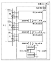
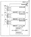
- FIG. 1 is a block diagram showing the overall configuration of an assembled battery system according to Embodiment 1.
- FIG. 2 is a block diagram showing the configuration of the voltage detection circuit according to the first embodiment.
- 3 is a block diagram showing a configuration of a communication circuit according to Embodiment 1.
- FIG. 4 is a block diagram showing the overall configuration of an assembled battery system according to Embodiment 2.
- FIG. 5 is a block diagram showing the configuration of the voltage detection circuit according to the second embodiment.
- FIG. 6 is a block diagram showing the configuration of a communication circuit according to the second embodiment.
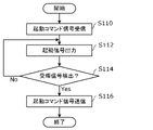
- FIG. 7 is a flow chart showing a method of outputting an activation signal according to the second embodiment.
- FIG. 8 is a flow chart showing a method for detecting an activation signal according to the second embodiment.
- FIG. 9 is a flowchart showing an alarm signal output method according to the second embodiment.
- FIG. 10 is a schematic diagram showing a first example of output timings of the alarm signal and the activation signal according to the second embodiment.
- FIG. 11 is a schematic diagram showing a second example of output timings of the alarm signal and the activation signal according to the second embodiment.
- FIG. 12 is a block diagram showing the overall configuration of an assembled battery system according to Embodiment 3. As shown in FIG. FIG. 13 is a block diagram showing the configuration of the voltage detection circuit according to the third embodiment. 14 is a block diagram showing a configuration of a communication circuit according to Embodiment 3.
- FIG. 15 is a flow chart showing a method of outputting an activation signal according to the third embodiment.
- FIG. 16 is a flow chart showing a method of detecting an activation signal according to the third embodiment.
- FIG. 17 is a flow chart showing an alarm signal output method according to the third embodiment.
- FIG. 18 is a schematic diagram showing a first example of output timings of the alarm signal, acceptance signal, and activation signal according to the third embodiment.
- FIG. 19 is a schematic diagram showing a second example of output timings of the alarm signal, acceptance signal, and activation signal according to the third embodiment.
- FIG. 20 is a block diagram showing the overall configuration of an assembled battery system according to Embodiment 4. As shown in FIG. FIG. 21 is a block diagram showing the configuration of the voltage detection circuit according to the fourth embodiment.
- each figure is a schematic diagram and is not necessarily strictly illustrated. Therefore, the scales and the like are not always the same in each drawing.
- symbol is attached
- Embodiment 1 A voltage measuring device and an assembled battery system according to Embodiment 1 will be described.
- FIG. 1 is a block diagram showing the overall configuration of an assembled battery system 1 according to this embodiment.
- the assembled battery system 1 is a system that supplies DC power. As shown in FIG. 1 , the assembled battery system 1 includes a voltage measuring device 10 and an assembled battery 8 .
- the assembled battery 8 has a plurality of battery modules 80, 80a, 80b connected in series.
- Each of the battery modules 80, 80a, 80b has a plurality of battery cells 81 connected in series.
- the configuration of the battery cell 81 is not particularly limited.
- a lithium ion battery can be used as the battery cell 81 .
- the voltage measuring device 10 is a device that measures the voltage of at least one battery cell 81 out of a plurality of battery cells 81 connected in series. In the present embodiment, voltage measuring device 10 measures the voltage of each of multiple battery cells 81 .
- the voltage measuring device 10 includes voltage detection circuits 40, 40a, and 40b. In the present embodiment, voltage measuring device 10 further includes communication circuit 30 and control circuit 20 .
- the voltage detection circuits 40, 40a, 40b are daisy-chained.
- the voltage measuring device 10 has a normal mode and a low power consumption mode as operation modes. In the low power consumption mode, the power consumption of the voltage detection circuit 40 and the like is limited, so voltage detection operation can be performed for a long time without charging the plurality of battery cells 81 .
- Each of the voltage detection circuits 40 , 40 a and 40 b is a circuit that detects voltages of the plurality of battery cells 81 .
- the voltage detection circuit 40 is an example of a first voltage detection circuit positioned at one end of the daisy-chained voltage detection circuits 40 , 40 a, and 40 b and is connected to the communication circuit 30 .
- the configuration of the voltage detection circuit 40 will be described with reference to FIG. 2 as a representative of the voltage detection circuits 40, 40a, and 40b.
- the voltage detection circuits 40 a and 40 b have the same configuration as the voltage detection circuit 40 .
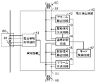
- FIG. 2 is a block diagram showing the configuration of the voltage detection circuit 40 according to this embodiment.
- the voltage detection circuit 40 includes a battery information acquisition circuit 41, a communication control circuit 44, a start signal detection circuit 45, an alarm generation circuit 46, a mode control circuit 47, and a first communication path. 51.
- the voltage detection circuit 40 further includes an alarm detection circuit 42 , an activation signal generation circuit 43 and a second communication path 52 .
- the first communication path 51 is one of two communication paths that constitute the daisy communication path of the voltage detection circuit 40 .
- a first communication path 51 of the voltage detection circuit 40 is connected to the communication circuit 30 via the isolation element 60 .
- isolation element 60 is a transformer.
- the insulating element 60 is not particularly limited as long as it is an element that can transmit a signal while maintaining electrical insulation.
- the isolation element 60 may be, for example, a capacitor, a photocoupler, or the like.
- the second communication path 52 is a communication path different from the first communication path 51.
- the second communication path 52 is the other of the two communication paths that make up the daisy communication path of the voltage detection circuit 40 .
- the second communication path 52 of the voltage detection circuit 40 is connected to the first communication path 51 of the voltage detection circuit 40a.
- the second communication path 52 of the voltage detection circuit 40a is connected to the first communication path 51 of the voltage detection circuit 40b. That is, of the plurality of daisy-chained voltage detection circuits, the second communication path 52 of one of the two voltage detection circuits connected to each other is connected to the first communication path 51 of the other of the two voltage detection circuits. be.
- the second communication path 52 of one of the two voltage detection circuits connected to each other is connected to the second communication path 52 of the other of the two voltage detection circuits via the insulating element 60 . It is connected to one communication path 51 .
- the battery information acquisition circuit 41 is a circuit that detects the voltage of at least one battery cell 81 out of the plurality of battery cells 81 . In this embodiment, the battery information acquisition circuit 41 detects the voltage of each of the plurality of battery cells 81 .
- the battery information acquisition circuit 41 may acquire information other than the voltages of the plurality of battery cells 81 . For example, the battery information acquisition circuit 41 may acquire the current flowing through the plurality of battery cells 81, the temperature of the plurality of battery cells 81, and the like.
- the battery information acquisition circuit 41 outputs abnormality information to the alarm generation circuit 46 when detecting that at least one of the plurality of battery cells 81 is abnormal.
- the battery information acquisition circuit 41 detects, for example, the voltage value of the battery cell 81 connected to the voltage detection circuit 40, compares the voltage value with a preset threshold value, and determines whether there is an abnormality in the voltage value. judge. If there is an abnormality in the voltage value, abnormality information corresponding to the abnormality is output to the alarm generation circuit 46 .
- the battery information acquisition circuit 41 includes, for example, an ADC (Analog-Digital Converter), converts an analog measurement value into a digital signal, and outputs the digital signal.
- ADC Analog-Digital Converter
- the alarm detection circuit 42 is an example of a first alarm detection circuit that detects an alarm signal input from the second communication path 52.
- the alarm signal is a signal used in the low power consumption mode and is used to notify the battery cell 81 of abnormality.
- the alarm detection circuit 42 outputs an alarm detection signal to the alarm generation circuit 46 when the alarm signal is detected.
- the alarm generation circuit 46 is a circuit that generates an alarm signal indicating an abnormality in the battery cell 81 and outputs it to the first communication path 51 in the low power consumption mode.
- the alarm generation circuit 46 generates an alarm signal based on the abnormality information from the battery information acquisition circuit 41 .
- the alarm generation circuit 46 outputs an alarm signal to the first communication path 51 when the alarm detection circuit 42 detects an alarm signal in addition to the abnormality information from the battery information acquisition circuit 41. . More specifically, when the alarm detection circuit 42 detects an alarm signal, it outputs the alarm detection signal to the alarm generation circuit 46 .
- the alarm generation circuit 46 outputs an alarm signal to the first communication path 51 when the alarm detection signal is input.
- the communication control circuit 44 is an example of a first communication control circuit that transmits and receives command signals from the first communication path 51 .
- command signals are transmitted and received through the first communication path 51 and the second communication path 52 .
- the communication control circuit 44 controls the voltage detection circuit 40 based on the received command signal. For example, when receiving the activation command signal from the first communication path 51 , the communication control circuit 44 causes the activation signal generation circuit 43 to output the activation signal to the second communication path 52 . Also, in the normal mode, when the communication control circuit 44 receives a mode change command signal, it causes the mode control circuit 47 to switch the operation mode to the low power consumption mode.
- the activation signal generation circuit 43 is an example of a first activation signal generation circuit that generates an activation signal and outputs it to the second communication path 52 .
- the activation signal is a signal for activating the voltage detection circuit 40 and the like in the low power consumption mode.
- the activation signal generation circuit 43 outputs the activation signal to the second communication path 52 when the communication control circuit 44 receives the activation command signal from the first communication path 51 .
- the activation signal detection circuit 45 is a circuit that detects the activation signal input from the first communication path 51 .
- the activation signal detection circuit 45 outputs an activation request signal to the mode control circuit 47 when the activation signal is detected.
- the mode control circuit 47 is a circuit that switches the operation mode of the voltage detection circuit 40 between a normal mode and a low power consumption mode that consumes less power than the normal mode. In the low power consumption mode, when the activation signal detection circuit 45 detects the activation signal, the mode control circuit 47 switches the operation mode to the normal mode. More specifically, when the activation signal detection circuit 45 detects the activation signal in the low power consumption mode, it outputs the activation request signal to the mode control circuit 47 . The mode control circuit 47 switches the operation mode to the normal mode when the activation request signal is input.
- the communication circuit 30 is a circuit that communicates with the control circuit 20 and the voltage detection circuits 40, 40a, and 40b.
- the communication circuit 30 is connected to the first communication path 51 of the voltage detection circuit 40 . In this embodiment, it is connected to the first communication path 51 of the voltage detection circuit 40 positioned at one end of the daisy-chained voltage detection circuits 40, 40a, and 40b.
- Communication circuit 30 according to the present embodiment will be described below with reference to FIG.
- FIG. 3 is a block diagram showing the configuration of communication circuit 30 according to this embodiment.
- FIG. 3 also shows the control circuit 20 . As shown in FIG.
- the communication circuit 30 includes a first communication path 71, a second communication path 72, an alarm detection circuit 32, an activation signal generation circuit 33, a communication control circuit 34 , a power converter 38 , and a power control circuit 39 .
- a first communication path 71 is a communication path connected to the control circuit 20 .
- the communication circuit 30 transmits and receives command signals to and from the control circuit 20 via the first communication path 71 . Since both the communication circuit 30 and the control circuit 20 operate using power from the low-voltage power supply, the insulating element 60 is not interposed between the first communication path 71 and the control circuit 20. may
- the second communication path 72 is a communication path connected to the first communication path 51 of the voltage detection circuit 40 .
- the second communication path 72 is connected to the first communication path 51 via the insulating element 60 .
- the alarm detection circuit 32 is an example of a second alarm detection circuit that detects an alarm signal.
- the alarm signal output from the voltage detection circuit 40 is input to the alarm detection circuit 32 via the first communication path 51 and the second communication path 72 .
- the alarm detection circuit 32 detects the alarm signal, the alarm detection circuit 32 notifies the control circuit 20 of the detection of the alarm signal.
- alarm detection circuit 32 outputs an alarm signal to control circuit 20 .
- the activation signal generation circuit 33 is an example of a second activation signal generation circuit that generates an activation signal. Upon receiving the activation command from the control circuit 20 , the activation signal generation circuit 33 outputs the activation signal to the first communication path 51 of the voltage detection circuit 40 .
- the control circuit 20 issues an activation command to the communication control circuit 34 when an alarm signal is input from the alarm detection circuit 32 or when the vehicle in which the assembled battery system 1 is installed is to be switched to the normal mode, such as when the vehicle is stopped. Send a signal.
- the communication control circuit 34 that has received the activation command signal causes the activation signal generation circuit 33 to output the activation signal.
- the communication control circuit 34 is an example of a second communication control circuit that transmits and receives command signals from the first communication path 71 and the second communication path 72.
- the power converter 38 is a device that converts the signal input to the second communication path 72 into a DC voltage. In this embodiment, power converter 38 converts the alarm signal to a DC voltage. Note that power may be supplied from outside the communication circuit 30 in the low power consumption mode instead of the power converter 38 .
- the power supply control circuit 39 is a circuit that controls power supply from a power supply (not shown) to the communication circuit 30 .
- the power supply control circuit 39 limits the power supply from the power supply in the low power consumption mode, and does not limit the power supply from the power supply in the normal mode.
- the power control circuit 39 may transmit a power state signal indicating the power state to the control circuit 20 . Further, the power supply control circuit 39 receives an activation request signal from the control circuit 20 and starts supplying power from the power supply to the communication circuit 30 when the supply of power from the power supply to the communication circuit 30 is interrupted.
- the control circuit 20 is a circuit that controls the voltage detection circuits 40, 40a, and 40b.
- control circuit 20 is connected to communication circuit 30 .
- the control circuit 20 controls the voltage detection circuits 40 , 40 a and 40 b via the communication circuit 30 by transmitting command signals to the communication circuit 30 .
- the control circuit 20 transmits an activation command signal to the first communication path 71 of the communication circuit 30 when an alarm signal is input from the alarm detection circuit 32 of the communication circuit 30 .
- the control circuit 20 can be implemented using, for example, an MCU (Micro-Controller Unit).
- the voltage measuring device 10 has a normal mode and a low power consumption mode as operation modes. The switching operation from the normal mode to the low power consumption mode in the voltage measuring device 10 will be described below.
- the control circuit 20 transmits a mode change command signal to the communication circuit 30 .
- the communication control circuit 34 of the communication circuit 30 that has received the mode change command signal transmits the mode change command signal to the first communication path 51 of the voltage detection circuit 40 .
- the communication control circuit 34 switches the operation mode of the communication circuit 30 to the low power consumption mode.
- the communication control circuit 44 of the voltage detection circuit 40 Upon receiving the mode change command signal, the communication control circuit 44 of the voltage detection circuit 40 transmits the mode change command signal to the voltage detection circuit 40a. After transmitting the mode change command signal, the communication control circuit 44 causes the mode control circuit 47 to switch the operation mode to the low power consumption mode. Thereby, the operation mode of the voltage detection circuit 40 is switched to the low power consumption mode. Similarly, the operation modes of the voltage detection circuits 40a and 40b are also switched to the low power consumption mode.
- the operation mode of the voltage measuring device 10 can be switched from the normal mode to the low power consumption mode.
- each voltage detection circuit lengthens the time interval for voltage detection of the battery cell 81 compared to the time interval in the normal mode, or restricts operations such as communication functions to reduce power consumption. Reduce power.
- a start command signal is transmitted from the control circuit 20 to the communication control circuit 34 of the communication circuit 30 .
- the communication control circuit 34 Upon receiving the activation command signal, the communication control circuit 34 causes the activation signal generation circuit 33 to output the activation signal.
- the activation signal is input to the first communication path 51 of the voltage detection circuit 40 via the second communication path 72 . Also, the communication control circuit 34 transmits the activation command signal to the first communication path 51 of the voltage detection circuit 40 via the second communication path 72 .
- the activation signal will be explained.
- the communication control circuit 44 and the like cannot receive command signals.
- the voltage detection circuit 40 and the like cannot recognize the content of the command signal even if it receives the command signal. Therefore, even in the low power consumption mode, a signal having a waveform that can be received by the voltage detection circuit 40 or the like is used as a start signal or the like.
- the activation signal is formed of a signal having a waveform whose level change interval (or period) is sufficiently larger than that of the command signal.
- Alarm signals and the like used in the low power consumption mode are also composed of waveform signals whose level change interval is sufficiently larger than that of the command signal, like the activation signal.
- Such an activation signal is detected by the activation signal detection circuit 45 .
- the activation signal detection circuit 45 causes the mode control circuit 47 to switch the operation mode to the normal mode when the activation signal is detected.
- the communication control circuit 44 After being switched to the normal mode, the communication control circuit 44 receives the activation command signal from the first communication path 51 . Upon receiving the activation command signal, the communication control circuit 44 causes the activation signal generation circuit 43 to output the activation signal.
- the operation mode of the voltage detection circuit 40 is switched from the low power consumption mode to the normal mode. Also, the voltage detection circuit 40 inputs an activation signal and transmits an activation command signal to the first communication path 51 of the voltage detection circuit 40a. As a result, the operation mode of the voltage detection circuit 40a is also switched to the normal mode in the same manner as the voltage detection circuit 40a. Thereafter, the operation mode of the voltage detection circuit 40b is similarly switched to the normal mode.
- the operating mode of the entire voltage measuring device 10 is switched from the low power consumption mode to the normal mode.
- each voltage detection circuit intermittently performs monitoring such as voltage detection of the battery cell 81 even in the low power consumption mode. For example, when the battery information acquisition circuit 41 of the voltage detection circuit 40 a detects an abnormality in the battery cell 81 or the like, the battery information acquisition circuit 41 outputs abnormality information indicating the abnormality in the battery cell 81 or the like to the alarm generation circuit 46 . do.
- the alarm generation circuit 46 to which the abnormality information is input generates an alarm signal corresponding to the abnormality information, and inputs the alarm signal from the first communication path 51 of the voltage detection circuit 40a to the second communication path 52 of the voltage detection circuit 40. do.
- the alarm detection circuit 42 detects the alarm signal and outputs the alarm detection signal to the alarm generation circuit 46 .
- the alarm generation circuit 46 outputs the alarm signal from the first communication path 51 to the second communication path 72 of the communication circuit 30 .
- the alarm detection circuit 32 of the communication circuit 30 detects the alarm signal and outputs the alarm signal to the control circuit 20 .
- the control circuit 20 transmits an activation command signal to the communication control circuit 34 of the communication circuit 30 when the alarm signal is input.
- the operation mode of each voltage detection circuit is switched to the normal mode in the same manner as the switching operation from the low power consumption mode to the normal mode.
- the voltage measuring device 10 enters a state in which it is possible to take measures against the abnormality, such as disconnecting the connection between the battery cell 81 and the load.
- the voltage measurement apparatus 10 uses the daisy communication paths of the voltage detection circuits 40, 40a, and 40b to transmit the voltage from the voltage detection circuit 40 to the communication circuit 30 even in the low power consumption mode. Alarm signal can be output.
- no communication path other than the daisy communication path is required, an increase in circuit size can be suppressed. Accordingly, the costs of the voltage measuring device 10 and the assembled battery system 1 can be suppressed.
- the power supply from the power supply is restricted in the low power consumption mode, but the power supply control circuit 39 may cut off the power supply from the power supply.
- the communication control circuit 34 of the communication circuit 30 receives the mode change command signal in the normal mode, the communication control circuit 34 of the communication circuit 30 transmits the mode change command signal and then causes the power supply control circuit 39 to cut off the power supply from the power supply.
- the power converter 38 converts the alarm signal into a DC voltage.
- Power converter 38 outputs a DC voltage to power supply control circuit 39 .
- the power supply control circuit 39 causes the power supply to start supplying power when the DC voltage is input.
- the power supply control circuit 39 outputs to the control circuit 20 a power supply status signal indicating the status of the power supply that has started supplying power. Based on the power status signal, the control circuit 20 detects that an alarm signal has been input to the communication circuit 30, and performs necessary processing such as switching the operation mode of each voltage detection circuit to the normal mode.
- a start request signal is output to the power supply control circuit 39 of the communication circuit 30.
- the power supply control circuit 39 causes the power supply to start supplying power to the communication circuit 30 when the activation request signal is input.
- the power supply from the power supply to the communication circuit 30 may be cut off in the low power consumption mode. Thereby, the power consumption of the voltage measuring device 10 in the low power consumption mode can be further reduced.
- Embodiment 2 A voltage measuring device and an assembled battery system according to Embodiment 2 will be described.
- the voltage measuring device according to the present embodiment differs from the voltage measuring device 10 according to the first embodiment mainly in that countermeasures are taken against collision between the activation signal and the alarm signal.
- the voltage measuring device and the assembled battery system according to the present embodiment will be described below, focusing on differences from the voltage measuring device 10 and the assembled battery system 1 according to the first embodiment.
- FIG. 4 is a block diagram showing the overall configuration of assembled battery system 101 according to the present embodiment.
- assembled battery system 101 includes voltage measuring device 110 and assembled battery 8 .
- the voltage measuring device 110 includes voltage detection circuits 140 , 140 a and 140 b , a communication circuit 130 and a control circuit 20 .
- FIG. 5 is a block diagram showing the configuration of the voltage detection circuit 140 according to this embodiment.
- the voltage detection circuit 140 includes a battery information acquisition circuit 41, a communication control circuit 44, a start signal detection circuit 45, an alarm generation circuit 46, a mode control circuit 47, and an alarm detection circuit 42. , an activation signal generation circuit 43 , an output instruction circuit 148 , a delay control circuit 149 , a first communication path 51 and a second communication path 52 .
- the output instruction circuit 148 is an example of a first output instruction circuit that causes the activation signal generation circuit 43 to output the activation signal multiple times at first time intervals.
- the first time interval is the time from when the output of one activation signal ends to when the output of the next activation signal starts.
- the first time interval may be greater than the output period of the alarm signal.
- the output instruction circuit 148 detects that the activation signal generation circuit 43 has output the first activation signal, and uses a timer to count the first time interval from the time when the output of the first activation signal is completed. . Subsequently, the output instruction circuit 148 causes the start signal generating circuit 43 to output the second start signal after the first time interval has passed since the output of the first start signal was completed.
- the output instruction circuit 148 may further cause the activation signal generation circuit 43 to output the activation signal.
- the delay control circuit 149 is a circuit that causes the alarm generation circuit 46 to output two consecutive alarm signals at a second time interval.
- the second time interval is the time from the end of the output of one alarm signal to the start of output of the next alarm signal.
- the second time interval may be greater than the sum of the first time interval and two output periods of the activation signal.
- the delay control circuit 149 detects that the alarm generation circuit 46 has output the first alarm signal, and counts the second time interval using a timer from the time when the output of the first alarm signal ends. Subsequently, the delay control circuit 149 causes the alarm generation circuit 46 to output the second alarm signal after the second time interval has elapsed since the output of the first alarm signal was completed.
- the delay control circuit 149 may further cause the alarm generation circuit 46 to output an alarm signal.
- FIG. 6 is a block diagram showing the configuration of communication circuit 130 according to the present embodiment.
- FIG. 6 also shows the control circuit 20 .
- the communication circuit 130 includes a first communication path 71, a second communication path 72, an alarm detection circuit 32, an activation signal generation circuit 33, a communication control circuit 34 , a power converter 38 , a power control circuit 39 , and an output instruction circuit 131 .
- the output instruction circuit 131 is an example of a second output instruction circuit that causes the activation signal generation circuit 33 to output the activation signal multiple times at first time intervals.
- the first time interval may be greater than the output period of the alarm signal.
- the output instruction circuit 131 causes the activation signal generation circuit 33 to output the activation signal multiple times at first time intervals.
- FIG. 7 is a flow chart showing a method for outputting a start signal according to this embodiment.
- FIG. 8 is a flow chart showing a method of detecting an activation signal according to this embodiment.
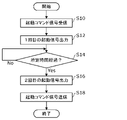
- FIG. 9 is a flow chart showing an alarm signal output method according to the present embodiment. 7 to 9 show how the voltage detection circuit 140 operates.
- the communication control circuit 44 first receives the activation command signal from the first communication path 51 (S10).
- voltage detection circuit 140 receives a start-up command signal from communication circuit 130 .
- the activation signal generation circuit 43 outputs the first activation signal (S12).
- the output instruction circuit 148 determines whether or not a predetermined time has passed (S14). If the predetermined time has not elapsed (No in S14), the output instruction circuit 148 repeats step S14. On the other hand, when the predetermined time has passed (Yes in S14), the output instruction circuit 148 causes the activation signal generation circuit 43 to output the activation signal for the second time (S16).
- the communication control circuit 44 transmits the activation command signal to the second communication path 52 (S18).
- the voltage detection circuit 140 can output the activation signal multiple times at the first time interval.
- the communication circuit 130 can also output the activation signal multiple times at first time intervals, similarly to the voltage detection circuit 140 .
- the activation signal detection circuit 45 of the voltage detection circuit 140 determines whether or not the activation signal input from the first communication path 51 is detected (S20). If the activation signal detection circuit 45 does not detect the activation signal (No in S20), step S20 is repeated. When the activation signal detection circuit 45 detects the activation signal (Yes in S20), the activation signal detection circuit 45 causes the mode control circuit 47 to switch the operation mode to the normal mode (S22).
- the voltage detection circuit 140 can detect the activation signal and switch the operation mode to the normal mode.
- the communication control circuit 44 of the voltage detection circuit 140 receives the mode change command signal from the first communication path 51 (S30).
- the communication control circuit 44 transmits a mode change command signal to the second communication path 52 (S32).
- the communication control circuit 44 causes the mode control circuit 47 to switch the operation mode to the low power consumption mode (S34).
- the alarm detection circuit 42 determines whether or not an alarm signal has been detected from the second communication path 52 (S36). If the alarm detection circuit 42 does not detect an alarm signal (No in S36), the alarm generation circuit 46 determines whether there is an input of abnormality information from the battery information acquisition circuit 41 (S38). On the other hand, when the alarm detection circuit 42 detects an alarm signal (Yes in S36), the process proceeds to step S40.
- step S40 When the alarm generation circuit 46 confirms that there is no anomaly information input (No in S38), the process returns to step S36. On the other hand, when the alarm generation circuit 46 confirms that there is an input of abnormality information (Yes in S38), the process proceeds to step S40.
- step S40 the voltage detection circuit 140 determines whether or not a predetermined time has passed since the previous alarm signal was output.
- the delay control circuit 149 of the voltage detection circuit 140 determines whether or not the second time interval has elapsed as the predetermined time. If the predetermined time has not elapsed (No in S40), step S40 is repeated. On the other hand, if the predetermined time has passed (Yes in S40), the alarm generation circuit 46 outputs an alarm signal to the first communication path 51 (S42).
- the voltage detection circuit 140 determines whether the operation mode is the low power consumption mode (S44). If the operation mode is the low power consumption mode (Yes in S44), the process returns to step S36. On the other hand, if the operation mode is not the low power consumption mode (No in S44), the alarm signal output operation is terminated.
- the voltage detection circuit 140 can output the alarm signal multiple times at second time intervals until the low power consumption mode is switched to the normal mode.
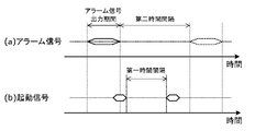
- FIG. 10 and 11 are schematic diagrams showing first and second examples, respectively, of the output timings of the alarm signal and the activation signal according to this embodiment.
- Graphs (a) of FIGS. 10 and 11 show the output timing of the alarm signal, and graphs (b) show the output timing of the activation signal.
- the alarm signal from the voltage detection circuit 140a and the voltage detection circuit 140 4 shows the output timing of each signal when the start signal from is output.
- the second activation signal is output at the first time interval from the end of the output of the first activation signal.
- the first time interval is longer than the output period of the alarm signal, the second activation signal can reliably avoid collision with the first alarm signal. Therefore, the second activation signal is reliably detected by the voltage detection circuit 140a. Thereby, the voltage detection circuit 140a is switched from the low power consumption mode to the normal mode.
- the operation mode of the voltage detection circuit 140a is switched to the normal mode after a second time interval from the end of the output of the first alarm signal, the purpose of the alarm signal is changed by switching to the normal mode. is also achieved, the second alarm signal is not output.
- the operation mode of the voltage detection circuit 140a has not been switched to the normal mode after the second time interval from the end of the output of the first alarm signal, the second alarm signal is output. Thereby, the operation mode can be switched more reliably. Since the second time interval is greater than the sum of the first time interval and two output periods of the activation signal, it is possible to reliably avoid the collision of the second alarm signal with the second activation signal.
- the second activation signal is output at the first time interval from the end of the output of the first activation signal, the second activation signal can reliably avoid collision with the first alarm signal. . Therefore, the second activation signal is reliably detected by the voltage detection circuit 140a. Thereby, the voltage detection circuit 140a is switched from the low power consumption mode to the normal mode. Note that if the operation mode of the voltage detection circuit 140a is switched to the normal mode after a second time interval from the end of the output of the first alarm signal, the second alarm signal is not output. On the other hand, if the operation mode of the voltage detection circuit 140a has not been switched to the normal mode after the second time interval from the end of the output of the first alarm signal, the second alarm signal is output. Thereby, the operation mode can be switched more reliably.
- the second time interval is larger than the sum of the first time interval and the two output periods of the activation signal, it is possible to reliably prevent the second alarm signal from colliding with the second activation signal.
- Embodiment 3 A voltage measuring device and an assembled battery system according to Embodiment 3 will be described.
- the voltage measuring device according to the present embodiment differs from the voltage measuring device 110 according to the second embodiment mainly in the collision avoidance method between the activation signal and the alarm signal.
- the voltage measuring device and the assembled battery system according to the present embodiment will be described below, focusing on differences from the voltage measuring device 110 and the assembled battery system 101 according to the second embodiment.
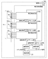
- FIG. 12 is a block diagram showing the overall configuration of an assembled battery system 201 according to this embodiment.
- assembled battery system 201 includes voltage measuring device 210 and assembled battery 8 .
- the voltage measuring device 210 includes voltage detection circuits 240 , 240 a and 240 b , a communication circuit 230 and a control circuit 20 .
- FIG. 13 is a block diagram showing the configuration of the voltage detection circuit 240 according to this embodiment.
- the voltage detection circuit 240 includes a battery information acquisition circuit 41, a communication control circuit 44, a start signal detection circuit 45, an alarm generation circuit 46, a mode control circuit 47, and an alarm detection circuit 42. , an activation signal generation circuit 43 , a reception signal detection circuit 248 , a reception signal generation circuit 249 , a first communication path 51 and a second communication path 52 .
- the acceptance signal generation circuit 249 is a circuit that outputs an acceptance signal when the activation signal detection circuit 45 detects the activation signal from the first communication path 51 . In this embodiment, the acceptance signal generation circuit 249 outputs the acceptance signal to the first communication path 51 .
- the acceptance signal detection circuit 248 is a circuit that detects the acceptance signal from the second communication path 52 . For example, when the acceptance signal detection circuit 248 does not detect the acceptance signal after the activation signal generation circuit 43 outputs the activation signal to the second communication path 52, the acceptance signal detection circuit 248 causes the activation signal generation circuit 43 to detect the activation signal. Make the signal output again.
- FIG. 14 is a block diagram showing the configuration of communication circuit 230 according to this embodiment.
- FIG. 14 also shows the control circuit 20 .
- the communication circuit 230 includes a first communication path 71, a second communication path 72, an alarm detection circuit 32, an activation signal generation circuit 33, a communication control circuit 34 , a power converter 38 , a power supply control circuit 39 , and a reception signal detection circuit 231 .
- the acceptance signal detection circuit 231 is a circuit that detects the acceptance signal from the second communication path 72 . For example, if the acceptance signal detection circuit 231 does not detect the acceptance signal after the activation signal generation circuit 33 outputs the activation signal to the second communication path 72, the activation signal generation circuit 33 outputs the activation signal again. In this embodiment, the acceptance signal detection circuit 231 causes the activation signal generation circuit 33 to output the activation signal again.
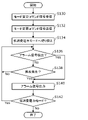
- FIG. 15 is a flow chart showing a method for outputting a start signal according to this embodiment.
- FIG. 16 is a flow chart showing a method for detecting an activation signal according to this embodiment.
- FIG. 17 is a flowchart showing an alarm signal output method according to this embodiment. 15 to 17 show how the voltage detection circuit 240 operates.
- the communication control circuit 44 first receives the activation command signal from the first communication path 51 (S110). In this embodiment, the voltage detection circuit 240 receives the activation command signal from the communication circuit 230 .
- the activation signal generation circuit 43 outputs the activation signal (S112).
- the acceptance signal detection circuit 248 determines whether or not the acceptance signal is detected (S114). If the acceptance signal detection circuit 248 has not detected the acceptance signal (No in S114), the acceptance signal detection circuit 248 causes the activation signal generation circuit 43 to output the activation signal again (S112). On the other hand, when the acceptance signal detection circuit 248 detects the acceptance signal (Yes in S114), the communication control circuit 44 transmits the activation command signal to the second communication path 52 (S116).
- the voltage detection circuit 240 repeatedly outputs the activation signal until the reception of the activation signal is confirmed. This allows the voltage detection circuit 240a to reliably detect the activation signal. Note that the communication circuit 230 also outputs a start signal in the same manner as the voltage detection circuit 240 .
- the activation signal detection circuit 45 of the voltage detection circuit 240 determines whether or not the activation signal input from the first communication path 51 is detected (S120). If the activation signal detection circuit 45 has not detected the activation signal (No in S120), step S120 is repeated. When the activation signal detection circuit 45 detects the activation signal (Yes in S120), the activation signal detection circuit 45 causes the acceptance signal generation circuit 249 to output the acceptance signal to the first communication path 51 (S122).
- the activation signal detection circuit 45 causes the mode control circuit 47 to switch the operation mode to the normal mode (S124).
- the voltage detection circuit 240 when the voltage detection circuit 240 detects the activation signal, it can output the acceptance signal and switch the operation mode to the normal mode.
- the communication control circuit 44 of the voltage detection circuit 240 receives the mode change command signal from the first communication path 51 (S130).
- the communication control circuit 44 transmits a mode change command signal to the second communication path 52 (S132).
- the communication control circuit 44 causes the mode control circuit 47 to switch the operation mode to the low power consumption mode (S134).
- the alarm detection circuit 42 determines whether or not an alarm signal has been detected from the second communication path 52 (S136). If the alarm detection circuit 42 does not detect an alarm signal (No in S136), the alarm generation circuit 46 determines whether there is an input of abnormality information from the battery information acquisition circuit 41 (S138). On the other hand, when the alarm detection circuit 42 detects an alarm signal (Yes in S136), the process proceeds to step S140.
- step S140 When the alarm generation circuit 46 confirms that there is no anomaly information input (No in S138), the process returns to step S136. On the other hand, when the alarm generation circuit 46 confirms that there is an input of abnormality information (Yes in S138), the process proceeds to step S140.
- step S140 the alarm generation circuit 46 outputs an alarm signal to the first communication path 51 (S140).
- the voltage detection circuit 240 determines whether the operation mode is the low power consumption mode (S142). If the operation mode is the low power consumption mode (Yes in S142), the process returns to step S136. On the other hand, if the operation mode is not the low power consumption mode (No in S142), the alarm signal output operation is terminated.
- the voltage detection circuit 240 can repeatedly output the alarm signal until the low power consumption mode is switched to the normal mode.
- FIG. 18 and 19 are schematic diagrams showing first and second examples, respectively, of the output timings of the alarm signal, acceptance signal, and activation signal according to this embodiment.
- Graphs (a) in FIGS. 18 and 19 show output timings of the alarm signal and the acceptance signal, and graphs (b) show output timings of the activation signal.
- the start signal detection circuit 45 of the voltage detection circuit 240a detects the start signal, and the acceptance signal generation circuit 249 generates the acceptance signal. Output.
- the acceptance signal is detected by the acceptance signal detection circuit 248 of the voltage detection circuit 240 .
- the voltage detection circuit 240 can confirm that the voltage detection circuit 240a has detected the activation signal, and therefore does not output the second activation signal.
- the purpose of the alarm signal is also achieved by switching to the normal mode, so the alarm signal is No output.
- the activation signal generation circuit 43 of the voltage detection circuit 240 outputs the activation signal for the second time.
- the activation signal detection circuit 45 of the voltage detection circuit 240a detects the activation signal, and the acceptance signal generation circuit 249 outputs the acceptance signal. do.
- the acceptance signal is detected by the acceptance signal detection circuit 248 of the voltage detection circuit 240 .
- the voltage detection circuit 240 can confirm that the voltage detection circuit 240a has detected the activation signal, and therefore does not output the activation signal for the third time.
- the activation signal generation circuit 43 of the voltage detection circuit 240 repeatedly outputs the activation signal until the acceptance signal detection circuit 248 detects the acceptance signal. Therefore, the activation signal can be reliably detected by the voltage detection circuit 240a.
- Embodiment 4 A voltage measuring device and an assembled battery system according to Embodiment 4 will be described.
- the voltage measuring device according to the present embodiment differs from the voltage measuring device 10 according to the first embodiment mainly in the connection configuration between the communication circuit and the plurality of voltage detection circuits.
- the voltage measuring device and the assembled battery system according to the present embodiment will be described below, focusing on differences from the voltage measuring device 10 and the assembled battery system 1 according to the first embodiment.
- FIG. 20 is a block diagram showing the overall configuration of an assembled battery system 301 according to this embodiment.
- assembled battery system 301 includes voltage measuring device 310 and assembled battery 8 .
- the voltage measuring device 310 includes voltage detection circuits 340 , 340 a and 340 b , communication circuits 30 and 30 a and a control circuit 20 .
- the communication circuits 30 and 30a are connected to the voltage detection circuits 340 and 340b at both ends of the daisy-chained voltage detection circuits 340, 340a and 340b, respectively.
- the communication circuit 30a has the same configuration as the communication circuit 30.
- the communication circuit 30 and the communication circuit 30a may be integrated into one communication circuit.
- FIG. 21 is a block diagram showing the configuration of the voltage detection circuit 340 according to this embodiment.
- the voltage detection circuit 340 includes a battery information acquisition circuit 41, a communication control circuit 344, a start signal detection circuit 345, an alarm generation circuit 346, a mode control circuit 47, and an alarm detection circuit 342. , an activation signal generation circuit 343 , a first communication path 51 , and a second communication path 52 .
- the alarm detection circuit 342 detects alarm signals input from the first communication path 51 and the second communication path 52 .
- the alarm detection circuit 342 outputs an alarm detection signal to the alarm generation circuit 346 when the alarm signal is detected.
- the alarm generation circuit 346 is a circuit that generates an alarm signal indicating an abnormality in the battery cell 81 and outputs it to at least one of the first communication path 51 and the second communication path 52 in the low power consumption mode. In the low power consumption mode, the alarm generation circuit 346 sends a signal to the second communication path 52 when the voltage detection circuit 340 detects an abnormality in the plurality of battery cells 81 or when the alarm detection circuit 342 detects an alarm signal. Output an alarm signal.
- the alarm generation circuit 346 when the alarm detection circuit 342 detects an alarm signal from the first communication path 51, the alarm generation circuit 346 outputs the alarm signal to the second communication path 52, and the alarm detection circuit 342 When an alarm signal is detected from the communication path 52 , the alarm signal is output to the first communication path 51 . More specifically, when alarm detection circuit 342 detects an alarm signal, it outputs an alarm detection signal to alarm generation circuit 346 . The alarm generation circuit 346 outputs an alarm signal when the alarm detection signal is input.
- the communication control circuit 344 transmits and receives command signals from the first communication path 51 and the second communication path 52 .
- command signals are transmitted and received through the first communication path 51 and the second communication path 52 .
- the activation signal generation circuit 343 outputs the activation signal to the first communication path 51 .
- the activation signal generation circuit 343 generates an activation signal and outputs it to the first communication path 51 or the second communication path 52 .
- the activation signal generation circuit 343 outputs the activation signal to the second communication path 52 when the communication control circuit 344 receives the activation command signal from the first communication path 51 . Further, the activation signal generation circuit 343 outputs the activation signal to the first communication path 51 when the communication control circuit 344 receives the activation command signal from the second communication path 52 .
- the activation signal detection circuit 345 is a circuit that detects activation signals input from the first communication path 51 and the second communication path 52 .
- the activation signal detection circuit 345 detects the activation signal input from the first communication path 51 or the second communication path 52, the activation signal detection circuit 345 outputs an activation request signal to the mode control circuit 47, thereby causing the mode control circuit 47 to
- the operation mode of the voltage detection circuit 340 is switched to the normal mode.
- the activation signal detection circuit 345 detects the activation signal input from the first communication path 51 , it causes the activation signal generation circuit 343 to output the activation signal to the second communication path 52 .
- the activation signal detection circuit 345 detects the activation signal input from the second communication path 52 , it causes the activation signal generation circuit 343 to output the activation signal to the first communication path 51 .
- the second communication path 52 of the voltage detection circuit 340b is connected to the second communication path 72 of the communication circuit 30a. Also, the first communication path 71 of the communication circuit 30 a is connected to the control circuit 20 .
- the operation of voltage measuring device 310 according to the present embodiment is such that the flow of each signal in communication circuits 30, 30a and voltage detection circuits 340, 340a, 340b corresponds to the flow of each signal in voltage measuring device 10 according to the first embodiment. differs from the operation of the voltage measuring device 10 according to the first embodiment in that it also operates in the direction opposite to the direction of .
- a voltage measuring device 310 for example, since the daisy communication path is configured in a ring, even if a part of the daisy communication path is blocked, signals can be transmitted and received using the unblocked part. . Therefore, the reliability of voltage measuring device 310 can be enhanced.
- the assembled battery system includes a communication circuit and a control circuit, but these circuits are not essential components.
- the voltage measurement device includes a plurality of voltage detection circuits, but the voltage measurement device may include a single voltage detection circuit. In other words, the voltage measuring device may have one or more voltage detection circuits.
- the voltage detection circuit includes a timer, and in the low power consumption mode, the timer is used to periodically measure the voltage of the battery cell 81, and the measurement result may be output as an alarm signal. good.
- the voltage detection circuit detects whether the measured voltage exceeds the upper limit (violation of the upper limit), falls below the lower limit (violation of the lower limit), or is within the normal range. may be output as an alarm signal. This allows the control circuit 20 to efficiently process the measurement results. By outputting an alarm signal indicating that the measured voltage is normal, it can be seen that the voltage of the battery cell 81 is being measured periodically.
- the voltage detection circuit may output information such as power supply voltage anomaly, temperature anomaly, and clock anomaly as an alarm signal.
- the activation signal generation circuit of the voltage detection circuit transmits the activation signal after the communication control circuit receives the activation command signal
- the activation signal may be output after the activation signal detection circuit detects the activation signal.
- the assembled battery system according to each of the above-described embodiments may be accommodated in, for example, one housing or may be separated into a plurality of units.
- a system LSI is an ultra-multifunctional LSI manufactured by integrating multiple components on a single chip. Specifically, it is a computer system that includes a microprocessor, ROM, RAM, etc. . A computer program is stored in the RAM. The system LSI achieves its functions by the microprocessor operating according to the computer program.
- IC card or module is a computer system composed of a microprocessor, ROM, RAM and the like.
- the IC card or module may include the super multifunctional LSI.
- the IC card or module achieves its function by the microprocessor operating according to the computer program. This IC card or this module may have tamper resistance.
- the present disclosure may be a computer system comprising a microprocessor and memory, the memory storing the computer program, and the microprocessor operating according to the computer program.
- each voltage measuring device according to the second or third embodiment may be combined with the voltage measuring device 310 according to the fourth embodiment.
- a voltage measuring device and an assembled battery system according to the present disclosure can be used, for example, as an assembled battery system for an in-vehicle assembled battery system.
- Reference Signs List 1 101, 201, 301 assembled battery system 8 assembled battery 10, 110, 210, 310 voltage measuring device 20 control circuit 30, 30a, 130, 230 communication circuit 32, 42, 342 alarm detection circuit 33, 43, 343 start signal Generation circuit 34, 44, 344 Communication control circuit 38 Power converter 39 Power supply control circuit 40, 40a, 40b, 140, 140a, 140b, 240, 240a, 240b, 340, 340a, 340b Voltage detection circuit 41 Battery information acquisition circuit 45 , 345 start signal detection circuit 46, 346 alarm generation circuit 47 mode control circuit 51, 71 first communication path 52, 72 second communication path 60 insulating element 80, 80a, 80b battery module 81 battery cell 131, 148 output instruction circuit 149 Delay control circuits 231, 248 Acceptance signal detection circuit 249 Acceptance signal generation circuit
Landscapes
- Engineering & Computer Science (AREA)
- Power Engineering (AREA)
- General Chemical & Material Sciences (AREA)
- Chemical & Material Sciences (AREA)
- Chemical Kinetics & Catalysis (AREA)
- Electrochemistry (AREA)
- Manufacturing & Machinery (AREA)
- Physics & Mathematics (AREA)
- General Physics & Mathematics (AREA)
- Microelectronics & Electronic Packaging (AREA)
- Measurement Of Current Or Voltage (AREA)
- Charge And Discharge Circuits For Batteries Or The Like (AREA)
- Secondary Cells (AREA)
Priority Applications (4)
| Application Number | Priority Date | Filing Date | Title |
|---|---|---|---|
| JP2023503966A JPWO2022186374A1 (https=) | 2021-03-05 | 2022-03-04 | |
| CN202280018110.3A CN116981948A (zh) | 2021-03-05 | 2022-03-04 | 电压测定装置及电池组系统 |
| EP22763424.3A EP4303593A4 (en) | 2021-03-05 | 2022-03-04 | VOLTAGE MEASURING DEVICE AND BATTERY PACK SYSTEM |
| US18/456,299 US20230408586A1 (en) | 2021-03-05 | 2023-08-25 | Voltage measurement device and cell stack system |
Applications Claiming Priority (4)
| Application Number | Priority Date | Filing Date | Title |
|---|---|---|---|
| US202163157251P | 2021-03-05 | 2021-03-05 | |
| US63/157,251 | 2021-03-05 | ||
| US202163244598P | 2021-09-15 | 2021-09-15 | |
| US63/244,598 | 2021-09-15 |
Related Child Applications (1)
| Application Number | Title | Priority Date | Filing Date |
|---|---|---|---|
| US18/456,299 Continuation US20230408586A1 (en) | 2021-03-05 | 2023-08-25 | Voltage measurement device and cell stack system |
Publications (1)
| Publication Number | Publication Date |
|---|---|
| WO2022186374A1 true WO2022186374A1 (ja) | 2022-09-09 |
Family
ID=83154485
Family Applications (4)
| Application Number | Title | Priority Date | Filing Date |
|---|---|---|---|
| PCT/JP2022/009389 Ceased WO2022186374A1 (ja) | 2021-03-05 | 2022-03-04 | 電圧測定装置、及び組電池システム |
| PCT/JP2022/009391 Ceased WO2022186376A1 (ja) | 2021-03-05 | 2022-03-04 | 組電池管理システム |
| PCT/JP2022/009390 Ceased WO2022186375A1 (ja) | 2021-03-05 | 2022-03-04 | 電圧測定システム |
| PCT/JP2022/009387 Ceased WO2022186373A1 (ja) | 2021-03-05 | 2022-03-04 | 電圧測定装置 |
Family Applications After (3)
| Application Number | Title | Priority Date | Filing Date |
|---|---|---|---|
| PCT/JP2022/009391 Ceased WO2022186376A1 (ja) | 2021-03-05 | 2022-03-04 | 組電池管理システム |
| PCT/JP2022/009390 Ceased WO2022186375A1 (ja) | 2021-03-05 | 2022-03-04 | 電圧測定システム |
| PCT/JP2022/009387 Ceased WO2022186373A1 (ja) | 2021-03-05 | 2022-03-04 | 電圧測定装置 |
Country Status (4)
| Country | Link |
|---|---|
| US (4) | US20230408586A1 (https=) |
| EP (4) | EP4304043A4 (https=) |
| JP (4) | JPWO2022186373A1 (https=) |
| WO (4) | WO2022186374A1 (https=) |
Families Citing this family (6)
| Publication number | Priority date | Publication date | Assignee | Title |
|---|---|---|---|---|
| JP7283218B2 (ja) * | 2019-05-10 | 2023-05-30 | オムロン株式会社 | 信号計測ユニット |
| JP7802530B2 (ja) * | 2021-12-28 | 2026-01-20 | 株式会社マキタ | 充電器 |
| US12259414B2 (en) * | 2022-08-18 | 2025-03-25 | Analog Devices International Unlimited Company | Synchronization mechanism for continous battery stack measurements |
| JP7785033B2 (ja) * | 2023-03-27 | 2025-12-12 | プライムプラネットエナジー&ソリューションズ株式会社 | 電圧測定用基板および蓄電システム |
| US20250349918A1 (en) * | 2024-02-15 | 2025-11-13 | Earth Top International Enterprises Ltd. | Sensory battery cell, intelligent battery using the sensory battery cell, power battery using the intelligent battery, battery management system and related method thereof |
| FR3161801A1 (fr) * | 2024-04-25 | 2025-10-31 | Pellenc Energy | Batterie comportant une pluralité de cellules de stockage d’énergie électrique et des circuits de surveillance individuelle des cellules |
Citations (12)
| Publication number | Priority date | Publication date | Assignee | Title |
|---|---|---|---|---|
| JPH08140204A (ja) * | 1994-11-08 | 1996-05-31 | Matsushita Electric Ind Co Ltd | 組電池の監視装置 |
| US20080049266A1 (en) * | 2006-07-07 | 2008-02-28 | Advmatch Technology, Inc. | Image sensor without opto-mechanical system and manufacturing method thereof |
| WO2010074290A1 (ja) * | 2008-12-28 | 2010-07-01 | 株式会社ソリトンシステムズ | 集積回路及びそれを用いた電池監視装置 |
| JP2013219936A (ja) * | 2012-04-09 | 2013-10-24 | Eliiy Power Co Ltd | 蓄電装置およびその制御方法ならびに電源装置 |
| WO2014038081A1 (ja) * | 2012-09-10 | 2014-03-13 | ルネサスエレクトロニクス株式会社 | 半導体装置及び電池電圧監視装置 |
| JP2015055503A (ja) * | 2013-09-10 | 2015-03-23 | ローム株式会社 | 電圧検出装置 |
| JP2015139292A (ja) * | 2014-01-22 | 2015-07-30 | トヨタ自動車株式会社 | 電池ユニット及び電池システム |
| US20160274637A1 (en) * | 2015-03-19 | 2016-09-22 | Samsung Electronics Co., Ltd. | Electronic apparatus and battery information providing method thereof |
| JP2017212877A (ja) * | 2017-08-10 | 2017-11-30 | ラピスセミコンダクタ株式会社 | 電池監視システム及び電池監視装置 |
| JP2018194336A (ja) * | 2017-05-12 | 2018-12-06 | 株式会社デンソーテン | 異常検知装置および異常検知方法 |
| US10180693B1 (en) * | 2017-10-05 | 2019-01-15 | Nuvoton Technology Corporation | Processing circuit and method thereof |
| JP2021018070A (ja) | 2019-07-17 | 2021-02-15 | 株式会社デンソー | 組電池監視装置 |
Family Cites Families (36)
| Publication number | Priority date | Publication date | Assignee | Title |
|---|---|---|---|---|
| JP2003115332A (ja) | 2002-07-04 | 2003-04-18 | Denso Corp | 組み電池の電圧検出装置 |
| KR100605425B1 (ko) * | 2004-10-18 | 2006-07-28 | 한국전자통신연구원 | 마이크로스트립형 대역통과필터 |
| GB0502274D0 (en) * | 2005-02-04 | 2005-03-09 | Xipower Ltd | Battery management system |
| JP5127383B2 (ja) * | 2007-09-28 | 2013-01-23 | 株式会社日立製作所 | 電池用集積回路および該電池用集積回路を使用した車両用電源システム |
| JP5065000B2 (ja) | 2007-12-28 | 2012-10-31 | 三洋電機株式会社 | 電圧測定装置及びこれを具えた組電池システム |
| JP5133926B2 (ja) * | 2009-03-26 | 2013-01-30 | 株式会社日立製作所 | 車両用電池システム |
| KR101016813B1 (ko) | 2009-05-19 | 2011-02-21 | 에스비리모티브 주식회사 | 배터리 관리 시스템 및 그 구동 방법 |
| JP2012154641A (ja) | 2011-01-21 | 2012-08-16 | Denso Corp | 電池状態監視装置 |
| JP5718731B2 (ja) * | 2011-05-31 | 2015-05-13 | ルネサスエレクトロニクス株式会社 | 電圧監視システム及び電圧監視モジュール |
| US9784813B2 (en) * | 2011-11-29 | 2017-10-10 | Hitachi, Ltd. | Battery control system and battery control method |
| JP2013207901A (ja) * | 2012-03-28 | 2013-10-07 | Sanyo Electric Co Ltd | 電池制御装置 |
| KR101362718B1 (ko) * | 2012-11-27 | 2014-02-13 | 현대오트론 주식회사 | 연속적 소프트웨어 리셋이 발생하는 전자 제어 장치에서의 고장 진단 방법 |
| JP5907050B2 (ja) * | 2012-12-10 | 2016-04-20 | 株式会社デンソー | 電池システム |
| DE102013225243A1 (de) | 2013-12-09 | 2015-06-11 | Robert Bosch Gmbh | Verfahren zum Übertragen eines minimalen und/oder eines maximalen Wertes eines Batteriesystemparameters und Batteriesystem zur Ausführung eines solchen Verfahrens |
| JP2015141062A (ja) | 2014-01-28 | 2015-08-03 | パナソニックIpマネジメント株式会社 | 組電池測定装置 |
| DE102014214996A1 (de) * | 2014-07-30 | 2016-02-04 | Robert Bosch Gmbh | Verfahren zum Betrieb eines Batteriesystems |
| JP2016075557A (ja) * | 2014-10-06 | 2016-05-12 | 三菱重工業株式会社 | 電池監視回路及び電池モジュール |
| JP6596818B2 (ja) * | 2014-12-10 | 2019-10-30 | 日立化成株式会社 | 蓄電池システム |
| JP2016115619A (ja) | 2014-12-17 | 2016-06-23 | トヨタ自動車株式会社 | 電池監視システム |
| JP2016151513A (ja) * | 2015-02-18 | 2016-08-22 | 日立オートモティブシステムズ株式会社 | 電池システム監視装置 |
| US10397668B2 (en) * | 2015-07-06 | 2019-08-27 | Panasonic Intellectual Property Management Co., Ltd. | Wakeup sequence for two-wire daisy chain communication system |
| JP6532831B2 (ja) * | 2016-01-28 | 2019-06-19 | 東芝デバイス&ストレージ株式会社 | 電圧監視回路及び電圧監視方法 |
| CN109792092B (zh) * | 2016-09-13 | 2022-03-18 | 三洋电机株式会社 | 管理装置和电源系统 |
| KR20180048069A (ko) * | 2016-11-02 | 2018-05-10 | 삼성에스디아이 주식회사 | 배터리 관리 시스템 |
| CN107234971A (zh) * | 2017-05-10 | 2017-10-10 | 深圳市沃特玛电池有限公司 | Bms唤醒系统及方法 |
| KR101977748B1 (ko) * | 2017-07-20 | 2019-05-13 | 현대오트론 주식회사 | 센싱 칩, 그것을 포함하는 배터리 관리 시스템 및 그것의 동작 방법 |
| CN207311148U (zh) * | 2017-08-18 | 2018-05-04 | 欣旺达电动汽车电池有限公司 | 一种电池管理装置 |
| DE102018100692B4 (de) * | 2018-01-12 | 2019-08-22 | Infineon Technologies Ag | Verfahren zum Überwachen einer Batterie, Überwachungssystem und Überwachungsschaltung |
| US10901045B2 (en) * | 2018-03-16 | 2021-01-26 | Infineon Technologies Ag | Battery diagnostics system and method using second path redundant measurement approach |
| JP7103026B2 (ja) * | 2018-07-30 | 2022-07-20 | 株式会社デンソー | 電池監視装置 |
| CN112640186B (zh) * | 2018-08-29 | 2024-12-06 | 新唐科技日本株式会社 | 单元监视电路以及管理系统 |
| JP7458326B2 (ja) * | 2018-12-17 | 2024-03-29 | ヌヴォトンテクノロジージャパン株式会社 | 電池監視制御回路 |
| CN113396503B (zh) * | 2019-01-31 | 2023-12-19 | 日本汽车能源株式会社 | 电池控制装置 |
| JP2020167616A (ja) | 2019-03-29 | 2020-10-08 | パナソニックIpマネジメント株式会社 | 時刻同期システムおよび中継装置 |
| CN111942216A (zh) * | 2019-04-29 | 2020-11-17 | 广州汽车集团股份有限公司 | 电池热失控监控方法、装置、系统及车辆 |
| CN211223102U (zh) * | 2019-12-31 | 2020-08-11 | 蜂巢能源科技有限公司 | 电池管理系统双向唤醒电路、电池管理系统及电动车辆 |
-
2022
- 2022-03-04 JP JP2023503965A patent/JPWO2022186373A1/ja active Pending
- 2022-03-04 EP EP22763426.8A patent/EP4304043A4/en active Pending
- 2022-03-04 JP JP2023503967A patent/JP7771158B2/ja active Active
- 2022-03-04 JP JP2023503968A patent/JP7739405B2/ja active Active
- 2022-03-04 JP JP2023503966A patent/JPWO2022186374A1/ja active Pending
- 2022-03-04 EP EP22763425.0A patent/EP4303594A4/en active Pending
- 2022-03-04 WO PCT/JP2022/009389 patent/WO2022186374A1/ja not_active Ceased
- 2022-03-04 EP EP22763423.5A patent/EP4303592A4/en active Pending
- 2022-03-04 WO PCT/JP2022/009391 patent/WO2022186376A1/ja not_active Ceased
- 2022-03-04 WO PCT/JP2022/009390 patent/WO2022186375A1/ja not_active Ceased
- 2022-03-04 WO PCT/JP2022/009387 patent/WO2022186373A1/ja not_active Ceased
- 2022-03-04 EP EP22763424.3A patent/EP4303593A4/en active Pending
-
2023
- 2023-08-25 US US18/456,299 patent/US20230408586A1/en active Pending
- 2023-08-25 US US18/456,273 patent/US20230400521A1/en active Pending
- 2023-08-28 US US18/457,068 patent/US20230400522A1/en active Pending
- 2023-08-28 US US18/457,113 patent/US20230402865A1/en active Pending
Patent Citations (12)
| Publication number | Priority date | Publication date | Assignee | Title |
|---|---|---|---|---|
| JPH08140204A (ja) * | 1994-11-08 | 1996-05-31 | Matsushita Electric Ind Co Ltd | 組電池の監視装置 |
| US20080049266A1 (en) * | 2006-07-07 | 2008-02-28 | Advmatch Technology, Inc. | Image sensor without opto-mechanical system and manufacturing method thereof |
| WO2010074290A1 (ja) * | 2008-12-28 | 2010-07-01 | 株式会社ソリトンシステムズ | 集積回路及びそれを用いた電池監視装置 |
| JP2013219936A (ja) * | 2012-04-09 | 2013-10-24 | Eliiy Power Co Ltd | 蓄電装置およびその制御方法ならびに電源装置 |
| WO2014038081A1 (ja) * | 2012-09-10 | 2014-03-13 | ルネサスエレクトロニクス株式会社 | 半導体装置及び電池電圧監視装置 |
| JP2015055503A (ja) * | 2013-09-10 | 2015-03-23 | ローム株式会社 | 電圧検出装置 |
| JP2015139292A (ja) * | 2014-01-22 | 2015-07-30 | トヨタ自動車株式会社 | 電池ユニット及び電池システム |
| US20160274637A1 (en) * | 2015-03-19 | 2016-09-22 | Samsung Electronics Co., Ltd. | Electronic apparatus and battery information providing method thereof |
| JP2018194336A (ja) * | 2017-05-12 | 2018-12-06 | 株式会社デンソーテン | 異常検知装置および異常検知方法 |
| JP2017212877A (ja) * | 2017-08-10 | 2017-11-30 | ラピスセミコンダクタ株式会社 | 電池監視システム及び電池監視装置 |
| US10180693B1 (en) * | 2017-10-05 | 2019-01-15 | Nuvoton Technology Corporation | Processing circuit and method thereof |
| JP2021018070A (ja) | 2019-07-17 | 2021-02-15 | 株式会社デンソー | 組電池監視装置 |
Non-Patent Citations (1)
| Title |
|---|
| See also references of EP4303593A4 |
Also Published As
| Publication number | Publication date |
|---|---|
| EP4304043A4 (en) | 2024-09-11 |
| EP4303594A4 (en) | 2024-09-18 |
| US20230408586A1 (en) | 2023-12-21 |
| JPWO2022186373A1 (https=) | 2022-09-09 |
| EP4303594A1 (en) | 2024-01-10 |
| JPWO2022186375A1 (https=) | 2022-09-09 |
| EP4304043A1 (en) | 2024-01-10 |
| JP7739405B2 (ja) | 2025-09-16 |
| EP4303592A1 (en) | 2024-01-10 |
| EP4303593A1 (en) | 2024-01-10 |
| JP7771158B2 (ja) | 2025-11-17 |
| US20230400522A1 (en) | 2023-12-14 |
| WO2022186376A1 (ja) | 2022-09-09 |
| EP4303593A4 (en) | 2024-09-18 |
| WO2022186373A1 (ja) | 2022-09-09 |
| US20230402865A1 (en) | 2023-12-14 |
| US20230400521A1 (en) | 2023-12-14 |
| JPWO2022186374A1 (https=) | 2022-09-09 |
| EP4303592A4 (en) | 2024-10-09 |
| WO2022186375A1 (ja) | 2022-09-09 |
| JPWO2022186376A1 (https=) | 2022-09-09 |
Similar Documents
| Publication | Publication Date | Title |
|---|---|---|
| WO2022186374A1 (ja) | 電圧測定装置、及び組電池システム | |
| KR101977748B1 (ko) | 센싱 칩, 그것을 포함하는 배터리 관리 시스템 및 그것의 동작 방법 | |
| US6489749B1 (en) | Battery state monitoring circuit having differentiating circuit | |
| JP5355224B2 (ja) | 複数組電池の電圧監視装置 | |
| EP3098895B1 (en) | Power supply control system, power supply control apparatus, and power supply control method | |
| US10351084B2 (en) | Power supply control system | |
| CN111605437B (zh) | 电池管理系统及电池管理方法 | |
| JP2013092397A (ja) | 電池監視装置 | |
| US10855093B2 (en) | Apparatus and method for monitoring batteries and storing data based on battery status | |
| EP2693617B1 (en) | Power supply apparatus, processing apparatus, information processing system, and method for controlling power supply | |
| CN111712987A (zh) | 电池管理设备和方法 | |
| CA2250675C (en) | On/off control device for power source unit | |
| EP2565971B1 (en) | Voltage detection device for fuel cell | |
| WO2023070558A1 (zh) | 电源管理系统、微控制单元、电池管理系统和电池 | |
| JP2014226020A (ja) | 電池監視装置 | |
| JP2015088868A (ja) | 電池監視部制御装置、電池監視システム | |
| US12050487B2 (en) | Electronic circuitry | |
| US12155255B2 (en) | Power supply device of system | |
| CN116981948A (zh) | 电压测定装置及电池组系统 | |
| KR20240153146A (ko) | 배터리 시스템 및 배터리 시스템의 모니터링 방법 | |
| JP5371651B2 (ja) | 車両用電源システムおよび通信装置 | |
| KR20220167988A (ko) | 마이크로 컨트롤러의 온도 측정을 위한 배터리 관리장치의 구성 및 그 제어방법 | |
| JP2015139292A (ja) | 電池ユニット及び電池システム | |
| JPH116885A (ja) | 発電手段を備えた電子機器 | |
| JP5678843B2 (ja) | 集積回路装置 |
Legal Events
| Date | Code | Title | Description |
|---|---|---|---|
| 121 | Ep: the epo has been informed by wipo that ep was designated in this application |
Ref document number: 22763424 Country of ref document: EP Kind code of ref document: A1 |
|
| WWE | Wipo information: entry into national phase |
Ref document number: 2023503966 Country of ref document: JP |
|
| WWE | Wipo information: entry into national phase |
Ref document number: 202280018110.3 Country of ref document: CN |
|
| WWE | Wipo information: entry into national phase |
Ref document number: 2022763424 Country of ref document: EP |
|
| ENP | Entry into the national phase |
Ref document number: 2022763424 Country of ref document: EP Effective date: 20231005 |
|
| NENP | Non-entry into the national phase |
Ref country code: DE |