WO2022181069A1 - 薄膜インダクタ素子及び薄膜可変インダクタ素子 - Google Patents
薄膜インダクタ素子及び薄膜可変インダクタ素子 Download PDFInfo
- Publication number
- WO2022181069A1 WO2022181069A1 PCT/JP2022/000296 JP2022000296W WO2022181069A1 WO 2022181069 A1 WO2022181069 A1 WO 2022181069A1 JP 2022000296 W JP2022000296 W JP 2022000296W WO 2022181069 A1 WO2022181069 A1 WO 2022181069A1
- Authority
- WO
- WIPO (PCT)
- Prior art keywords
- layer
- thin film
- inductor element
- magnetic
- spin
- Prior art date
- Legal status (The legal status is an assumption and is not a legal conclusion. Google has not performed a legal analysis and makes no representation as to the accuracy of the status listed.)
- Ceased
Links
Images




Classifications
-
- H—ELECTRICITY
- H01—ELECTRIC ELEMENTS
- H01F—MAGNETS; INDUCTANCES; TRANSFORMERS; SELECTION OF MATERIALS FOR THEIR MAGNETIC PROPERTIES
- H01F21/00—Variable inductances or transformers of the signal type
- H01F21/02—Variable inductances or transformers of the signal type continuously variable, e.g. variometers
- H01F21/08—Variable inductances or transformers of the signal type continuously variable, e.g. variometers by varying the permeability of the core, e.g. by varying magnetic bias
-
- H—ELECTRICITY
- H01—ELECTRIC ELEMENTS
- H01F—MAGNETS; INDUCTANCES; TRANSFORMERS; SELECTION OF MATERIALS FOR THEIR MAGNETIC PROPERTIES
- H01F10/00—Thin magnetic films, e.g. of one-domain structure
- H01F10/32—Spin-exchange-coupled multilayers, e.g. nanostructured superlattices
-
- H—ELECTRICITY
- H10—SEMICONDUCTOR DEVICES; ELECTRIC SOLID-STATE DEVICES NOT OTHERWISE PROVIDED FOR
- H10D—INORGANIC ELECTRIC SEMICONDUCTOR DEVICES
- H10D1/00—Resistors, capacitors or inductors
- H10D1/20—Inductors
-
- H—ELECTRICITY
- H01—ELECTRIC ELEMENTS
- H01F—MAGNETS; INDUCTANCES; TRANSFORMERS; SELECTION OF MATERIALS FOR THEIR MAGNETIC PROPERTIES
- H01F10/00—Thin magnetic films, e.g. of one-domain structure
- H01F10/32—Spin-exchange-coupled multilayers, e.g. nanostructured superlattices
- H01F10/324—Exchange coupling of magnetic film pairs via a very thin non-magnetic spacer, e.g. by exchange with conduction electrons of the spacer
- H01F10/329—Spin-exchange coupled multilayers wherein the magnetisation of the free layer is switched by a spin-polarised current, e.g. spin torque effect
-
- H—ELECTRICITY
- H01—ELECTRIC ELEMENTS
- H01F—MAGNETS; INDUCTANCES; TRANSFORMERS; SELECTION OF MATERIALS FOR THEIR MAGNETIC PROPERTIES
- H01F17/00—Fixed inductances of the signal type
- H01F17/02—Fixed inductances of the signal type without magnetic core
-
- H—ELECTRICITY
- H01—ELECTRIC ELEMENTS
- H01F—MAGNETS; INDUCTANCES; TRANSFORMERS; SELECTION OF MATERIALS FOR THEIR MAGNETIC PROPERTIES
- H01F21/00—Variable inductances or transformers of the signal type
- H01F21/005—Inductances without magnetic core
-
- H—ELECTRICITY
- H10—SEMICONDUCTOR DEVICES; ELECTRIC SOLID-STATE DEVICES NOT OTHERWISE PROVIDED FOR
- H10N—ELECTRIC SOLID-STATE DEVICES NOT OTHERWISE PROVIDED FOR
- H10N50/00—Galvanomagnetic devices
- H10N50/20—Spin-polarised current-controlled devices
-
- H—ELECTRICITY
- H10—SEMICONDUCTOR DEVICES; ELECTRIC SOLID-STATE DEVICES NOT OTHERWISE PROVIDED FOR
- H10N—ELECTRIC SOLID-STATE DEVICES NOT OTHERWISE PROVIDED FOR
- H10N50/00—Galvanomagnetic devices
- H10N50/80—Constructional details
-
- B—PERFORMING OPERATIONS; TRANSPORTING
- B82—NANOTECHNOLOGY
- B82Y—SPECIFIC USES OR APPLICATIONS OF NANOSTRUCTURES; MEASUREMENT OR ANALYSIS OF NANOSTRUCTURES; MANUFACTURE OR TREATMENT OF NANOSTRUCTURES
- B82Y25/00—Nanomagnetism, e.g. magnetoimpedance, anisotropic magnetoresistance, giant magnetoresistance or tunneling magnetoresistance
Definitions
- the present invention relates to thin film inductor elements and thin film variable inductor elements.
- An inductor element is known as an element that uses an induced electromotive force generated in a coil to keep a circuit current constant. While transformers for transforming are the primary applications, inductor elements are also used as high-frequency circuits such as filters in small electrical devices and electrical circuits. Miniaturization and miniaturization are required for circuit elements used in various electronic devices such as portable communication terminals. A certain degree of magnitude is required for the inductance, which is the strength of the inductor element. However, the inductance is proportional to the square of the number of turns of the coil and the cross-sectional area of the coil, and there is a trade-off relationship between the strength of the inductance and miniaturization.
- Non-Patent Document 1 does not have a trade-off relationship between inductance strength and miniaturization, as shown in FIG. 9, which is a comparison explanation with the conventional induction coil. Another characteristic is that the cross-sectional area of the element is inversely proportional to the inductance, and the inductance increases as the size is reduced. Therefore, emergent inductors are expected to greatly contribute to downsizing.
- Non-Patent Document 1 confirms that a non-collinear magnetic structure is formed by using Gd 3 Ru 4 Al 12 .
- Gd3Ru4Al12 cannot be said to be a common material, emergent inductors will have to select materials to realize them, and even if the problem of proper material selection is cleared, Crystallographic orientation control is also required to form a helical magnetic structure.
- the present invention provides a new type of thin-film inductor element that utilizes a new type of emergent magnetic field that is not so difficult to select a material and has not so high temperature dependence. This is the subject of the invention.
- a thin film inductor element of the present invention has at least the following configuration.
- the thin film variable inductor element of the present invention has at least the following configuration.
- the body layer and the nonmagnetic layer or the antiferromagnetic layer are extended in an arbitrary shape in a direction orthogonal to the lamination direction, and the vertical direction of the lamination direction is also arbitrary, and the magnetic layer is It has a substantially uniform magnetization structure, the pair of electrodes are provided at both ends where the laminated film is extended, an alternating current or a high frequency current is applied, and the barrier layer is the non-magnetic layer or
- the gate electrode layer is further laminated on the surface on the antiferromagnetic layer side, the gate electrode layer is further laminated on the barrier layer, and a positive and negative bias is applied to the gate electrode layer.
- the thin film variable inductor element of the present invention has at least the following configuration. a laminated film in which a magnetic layer and a nonmagnetic layer or an antiferromagnetic layer are laminated; a pair of electrodes for applying an alternating current or a high frequency current; and a thin film coil surrounding the laminated film,
- the body layer and the nonmagnetic layer or the antiferromagnetic layer are extended in an arbitrary shape in a direction orthogonal to the lamination direction, and the vertical direction of the lamination direction is also arbitrary, and the magnetic layer is It has a substantially uniform magnetization structure, and is characterized in that an inductance modulation operation is realized by controlling an external magnetic field by switching on/off the thin film coil and/or switching the direction of current.
- laminated film naturally includes a two-layer film consisting of a magnetic layer and a non-magnetic or antiferromagnetic layer. It also includes those to which additional membranes such as layers have been added.
- arbitrary shape means that any shape such as square, circle, ellipse, or rectangle may be used. intended.
- a pair of electrodes are provided at both ends along which the laminated film is stretched” means that the height position in the lamination direction of the electrodes is irrelevant, and that the individual electrodes It is intended to include a mode in which the height positions of are not aligned.
- substantially uniform magnetization structure refers to non-collinear magnetic structures such as spiral magnetic structures and horizontal conical magnetic structures, which are essential requirements for realizing emergent inductance in Non-Patent Document 1. Instead, it refers to a magnetic structure in which adjacent magnetic moments are collinearly aligned, including some non-uniformity due to temperature and material imperfections.
- FIG. 1A and 1B are a perspective view, a cross-sectional view, and a plan view showing the structural concept of a thin film inductor element according to an embodiment of the present invention
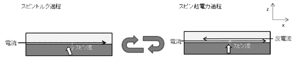
- FIG. 4 is an explanatory diagram showing the inductance operation of the thin film inductor element according to the embodiment of the present invention
- 1A and 1B are a perspective view, a cross-sectional view, and a plan view showing the structural concept of a thin film variable inductor element according to an embodiment of the present invention
- FIG. 5 is a diagram for explaining inductance modulation operation of the thin film variable inductor element according to the embodiment of the present invention
- 3A and 3B are a perspective view, a cross-sectional view, and a plan view showing the structural concept of another example of the thin film variable inductor element according to the embodiment of the present invention
- FIG. FIG. 10 is a diagram illustrating inductance modulation operation of another example of the thin film variable inductor element according to the embodiment of the present invention
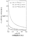
- FIG. 4 is a diagram showing inductance characteristics of a thin film variable inductor element according to an embodiment of the invention
- FIG. 5 is a diagram showing inductance characteristics of another example of the thin film variable inductor element according to the embodiment of the present invention
- FIG. 10 is a diagram for explaining a comparison between a conventional induction coil and an emergent inductor;
- the thin film inductor element and the thin film variable inductor element according to the embodiments of the present invention utilize spintronics technology or an emergent magnetic field, similar to the prior art emergent inductor. Emergent inductors were first found to be used as inductors by utilizing a combination of spin-transfer torque (STT) and its inverse process, spin electromotive force. Naturally, it does not focus on spin-orbit torque (SOT). Embodiments of the present invention, on the other hand, utilize a combination of spin-orbit torque (SOT) and its inverse. Spin-orbit torque (SOT) has already been researched and developed in fields such as magnetoresistive memory.
- the inductor is formed of a laminated film in which a heavy metal layer is laminated on a magnetic layer. It extends in the x-direction, and electrodes (not shown) are provided at both ends thereof, and alternating current or high-frequency current is applied.
- the z position where the electrode is provided can be any position near the heavy metal layer, near the magnetic layer, or near the boundary between the two.
- the vertical relationship between the heavy metal layer and the magnetic layer is arbitrary, and even if the vertical position is reversed from that shown, the inductor functions under the same conditions.
- a common module with a thin film variable inductor element which will be described later, is taken into account, it is advantageous to adopt the illustrated vertical relationship.
- the direction of magnetization of the magnetic material has stable magnetic anisotropy in the direction parallel to the lamination direction, as indicated by the white arrow in FIG.
- this magnetic anisotropy has been described only for the embodiments, and as already described, inductance is developed if a substantially uniform magnetization structure is formed.
- inductance can be developed in any non-magnetic layer capable of generating spin-orbit torque, without being limited to heavy metal layers. Needless to say, no external magnetic field is required, which is required for the magnetic reversal operation of the magnetoresistive memory.
- Inductor operation is achieved by alternating spin torque and spin electromotive force processes. It is easy to understand that this is the spintronics version of Lenz's law of electromagnetic induction, which states that when an induced current is generated by some cause, the direction of current flow coincides with the direction that hinders the cause of the induced current. A specific description will be given below.
- spin torque process current is introduced into the thin film inductor element according to the embodiment of the present invention.
- spins in the depth direction (y direction) of the paper are accumulated at the interface between the magnetic layer and the heavy metal layer, and a spin orbit torque acts on the magnetization of the magnetic layer.
- the magnetization direction is tilted from the direction perpendicular to the substrate (z direction) in which energy is stable.
- Mechanisms of spin accumulation include the "spin Hall effect" and the "Rashba effect”.
- the “spin Hall effect” is an effect in which the trajectories of electrons spin-polarized in the +y direction and electrons spin-polarized in the ⁇ y direction in the heavy metal layer are bent in opposite directions in the z direction, that is, ⁇ z This is the effect of generating a spin current in the direction. Therefore, only electrons spin-polarized in one direction in the y direction flow into the magnetic layer.
- the “Rashba effect” means that an effective electric field is generated at the interface between the heavy metal layer and the magnetic layer, and the interaction between the electric field and the momentum of conduction electrons causes either +y or -y This is the effect that only directionally spin-polarized conduction electrons accumulate at the interface.
- FIG. 2 illustrates a spin current generated by the spin Hall effect.
- the relationship between the direction of the current and the spin current is determined by the sign of the spin Hall effect.
- FIG. 2 shows a case where a spin current flows in the -z direction when a current flows in the +x direction (conversely, a spin current flows in the +z direction when a current flows in the -x direction).
- This directional relationship changes depending on the layer material.
- the sign of the current changes the sign of the spin current.
- the spin polarization component of the accumulated electrons can be changed, and the direction of the spin orbit torque acting on the magnetization of the magnetic layer can be reversed. Therefore, by inputting an alternating current, an alternating torque is generated.
- the current introduced into the inductor is an alternating current
- the magnetization of the magnetic layer precesses at the alternating current frequency of the input current.
- the magnetic energy stored in the magnetization tilted from the energy-stable substrate perpendicular direction (z) is the origin, and the precession of the magnetization produces a spin current.
- a countercurrent is generated in the direction that cancels out the current introduced into the inductor.
- the sum of the introduced current and the countercurrent flows through the inductor, realizing an action (inductor) that prevents changes in the current.
- an antiferromagnetic material instead of a heavy metal.
- X 30-70 at.% in Pt X Mn 100-X and Ir X Mn 100-X is preferable.
- a typical film thickness of the heavy metal layer or the antiferromagnetic layer is 2 nm or more and 20 nm or less.
- the magnetic layer is composed of a ferromagnetic material, a ferrimagnetic material, and an antiferromagnetic material (Note: it is also possible for the laminated film to consist of two layers, an antiferromagnetic layer/antiferromagnetic layer). It is a material containing Fe, Co, Ni, and Mn. For embodiments having an in-plane easy axis of magnetization, in particular, Ni--Fe alloys, Co--Fe--B alloys, etc. can be used.
- Co/Ni, Co/Pt, Co/Pd, Co/Au, Fe/Au stacks, Co-Pt, Co-Cr-Pt, Co- Pd, Fe-Pt, Fe-Pd, Fe-Co-Pt, Fe-Co-Pd alloy, CoFeB, FeB alloy, etc. can be used. good.
- the typical film thickness of the magnetic layer used in conventional magnetoresistive memories is 0.8 nm or more and 5 nm or less. In the inductor element, as described with reference to FIG. 2, it is sufficient if the magnetization direction can be tilted from the direction perpendicular to the substrate (z direction) where energy is stable. .
- the film thickness should be set appropriately according to the required performance. If each film of the two-layer film has the same shape, inductance can be expressed even if any shape such as a square, circle, ellipse, or rectangle is selected as the planar shape of the laminated film. However, from a practical point of view, it would be advantageous to choose a rectangular shape.
- the inductor element is shown as being composed of two layers, a magnetic layer and a heavy metal layer. A laminated film provided with a base layer, a cap layer for protecting the element during the process of microfabrication, or the like may be used.
- the first is a film configuration of Si sub./Ta(3)/CoFeB(1)/MgO(1.3)/Ta(1) from the substrate side.
- the magnitude of the spin-orbit torque effective magnetic field per current density generated in this case was 1.1 ⁇ 10 ⁇ 11 [mT/(A/m 2 )], and the inductance in this case was 0.0065 [nH].
- the second is a film configuration of Si sub./W(3)/CoFeB(1.3)/MgO(1.3)/Ta(1) from the substrate side.
- the magnitude of the spin-orbit torque effective magnetic field per current density generated in this case was 9.0x10 -11 [mT/(A/m 2 )], and the inductance in this case was 1.0 [nH].
- the third is a film configuration of Si sub./Ta(2)/Pt(3)/Co(1.6)/MgO(2)/Ta(1) from the substrate side.
- the magnitude of the spin-orbit torque effective magnetic field per current density generated in this case was 1.4 ⁇ 10 ⁇ 11 [mT/(A/m 2 )], and the inductance in this case was 0.04 [nH].
- the film structure was Ru(1).
- the magnitude of the spin-orbit torque effective magnetic field per current density generated in this case was 4.2 ⁇ 10 ⁇ 11 [mT/(A/m 2 )], and the inductance in this case was 0.1 [nH].
- the inductance when manufacturing the same size inductor with an air-core solenoid coil is estimated as follows. Assume that the inductor has a length of 100 ⁇ m, a width of 100 nm, and a thickness of 10 nm, and the winding density of the solenoid coil is assumed to be one turn per 100 nm, which is a value that can be achieved with current microfabrication technology.
- the inductor element based on the principle of the present invention can be realized only by processing the laminated film into a thin wire, the manufacturing cost can be significantly reduced compared to the classical inductor. That is, the thin film inductor element according to the embodiments of the present invention can realize the same or much higher inductance at a much lower cost than the conventional classical inductor.
- the thin film inductor element according to the embodiment of the present invention is also advantageous for emergent inductors that utilize a combination of spin-transfer torque (STT) and its inverse process, spin electromotive force.
- STT spin-transfer torque
- the emergent inductor requires the formation of a non-collinear magnetic structure such as a helical magnetic structure, and the material that exhibits this structure is special and unsuitable for mass production.
- the thin film inductor element it is sufficient to use a standard magnetic material having a collinear magnetic structure.
- the axis of easy magnetization is determined perpendicular to the film surface due to the structure of the double film, and the element can be manufactured by simple film formation, and the inductance can be realized at overwhelmingly low cost.
- Emergent inductors also have other advantages in terms of efficiency. According to previous research, the emergent inductor was made of Gd3Ru4Al12 , a rather special material, and exhibited inductance at extremely low temperatures of 16K or lower. No function was expressed. Of course, materials that exhibit inductance functions in higher temperature ranges may be discovered in the future, but this is limited to the temperature range in which non-collinear magnetic structures, including helical magnetism, appear on the magnetic phase diagram. , there are still restrictions on the operating environment temperature. In any case, there are still big hurdles to use in the normal temperature or higher temperature range.
- the thin film inductor element according to the embodiment of the present invention Ni-Fe alloy, Co-Fe-B alloy, Co/Ni, Co/Pt, Co/Pd, Co/Au, Fe/Au laminated films , Co-Pt, Co-Cr-Pt, Co-Pd, Fe-Pt, Fe-Pd, Fe-Co-Pt, Fe-Co-Pd alloys, CoFeB, and FeB alloys. and they work well at normal temperatures. Therefore, the thin film inductor element according to the embodiment of the present invention has few obstacles to practical use.
- FIG. 3A and 3B are a perspective view, a cross-sectional view, and a plan view showing the structural concept of the thin film variable inductor element according to the embodiment of the present invention.
- An inductor is formed of a double-layered film in which a heavy metal layer is laminated on a magnetic layer, is extended in the x-direction, is provided with electrodes (not shown) at both ends, and is applied with an alternating current, as shown in FIG. It is similar to the thin film inductor element.
- a barrier layer made of an insulator is laminated adjacent to the surface of the heavy metal layer of the two-layer film.
- materials include MgO, Al 2 O 3 , and AlN, but it is important to develop perpendicular magnetic anisotropy due to interface magnetic anisotropy between the barrier layer and the recording layer. /MgO and FeB/MgO are preferred.
- the direction of the axis of easy magnetization is arbitrary, and may be oriented in the x direction, for example.
- a gate electrode layer made of metal is further laminated on the barrier layer.
- metals with good conductivity such as Ta, Ru, and Cu, are suitable.
- the shape of the gate electrode layer is set to fit inside the barrier layer in the xy plane. This is to prevent the gate electrode layer from being electrically short-circuited with the inductor.
- the plane shape of the two-layer film can be any shape such as a square, circle, ellipse, or rectangle, as in the case of the thin film inductor element.
- the direction of magnetization of the magnetic material has stable magnetic anisotropy in the direction parallel to the lamination direction, as indicated by the white arrows in FIG.
- this magnetic anisotropy has been described only for the embodiments, and inductance is developed if a substantially uniform magnetization structure is formed.
- inductance can be developed in any non-magnetic layer capable of generating spin-orbit torque, without being limited to heavy metal layers. Needless to say, no external magnetic field is required, which is required for the magnetic reversal operation of the magnetoresistive memory.
- the inductance generated at the bilayer boundary will be modulated.
- a negative bias is applied to the gate electrode layer, holes accumulate at the junction interface with the insulating layer of the inductor, creating a local electric field opposite to that described above.
- a change in the spin-orbit interaction due to the electric field effect has a component proportional to the electric field and a component proportional to the square of the electric field. For this reason, it is not always possible to expect a reverse modulation effect at positive bias and negative bias. A modulated operation becomes feasible.
- the thin film variable inductor element according to the embodiment of the present invention can realize high-speed variable inductance by electrical control without mechanical operation by performing inductance operation in the presence of bias.
- STT spin-transfer torque
- spin electromotive force changes in inductance due to temperature and magnetic fields have been observed, but there are It is extremely difficult to control because it requires a large magnetic field of Tesla.
- the thin film variable inductor element according to the embodiment of the present invention using a simple metal double layer film has a small change in temperature and can be controlled by an electric field orthogonal to the current path, and has extremely high controllability. Become.
- FIG. 5 is a perspective view, cross-sectional view, and plan view showing the structural concept of a thin film variable inductor element that functions by applying an external magnetic field.
- An inductor is formed of a double-layered film in which a heavy metal layer is laminated on a magnetic layer, is extended in the x direction, is provided with electrodes (not shown) at both ends, and is applied with an alternating current, as shown in FIG. It is similar to the thin film variable inductor element.
- the locations where the electrodes are provided and the shape of the two-layer film also have a high degree of freedom, like the thin film variable inductor element shown in FIG. That is, as the planar shape of the two-layer film, any shape such as a square, circle, ellipse, or rectangle can be selected.
- the direction of magnetization of the magnetic material has stable magnetic anisotropy in the direction parallel to the lamination direction, as indicated by the white arrows in FIG. However, this magnetic anisotropy has been described only for the embodiments, and inductance is developed if a substantially uniform magnetization structure is formed.
- inductance can be developed in any non-magnetic layer capable of generating spin-orbit torque, without being limited to heavy metal layers.
- the difference from the thin film variable inductor element shown in FIG. 3 is that a thin film coil surrounding the laminated film is provided instead of the gate electrode.
- a circuit that controls the thin-film coil can control the Oersted magnetic field penetrating the inductor element in the stacking direction by turning on/off the current or switching the direction of the current.
- RSOC Rashba spin-orbit coupling
- ⁇ R is a parameter characterizing the magnitude of RSOC
- e is the elementary charge
- m (vector) is a unit vector representing the direction of uniform magnetization
- e z (vector) is the film thickness direction.
- the (z-direction) unit vector, ⁇ is a dimensionless parameter that characterizes the non-adiabatic dynamics of conduction electron spins.
- the magnetization is assumed to undergo small-angle precession about the z-direction. That is, it is represented by [Formula 3].
- ⁇ is the angular frequency of the alternating current input from the outside.
- SMF is calculated as [Formula 4]. Therefore, the inductance L caused by the SMF can be obtained by calculating [Equation 5] from the definition.
- Im[ ] is a symbol taking the imaginary part of a complex number
- A is the cross-sectional area of the sample perpendicular to the x-direction.
- [Formula 6] is obtained by substituting [Formula 4] for the voltage.
- Re[ ] is a symbol that takes the real part of a complex number.
- the sign of L is defined to be a positive value when the SMF acts in the opposite direction to the external current source.
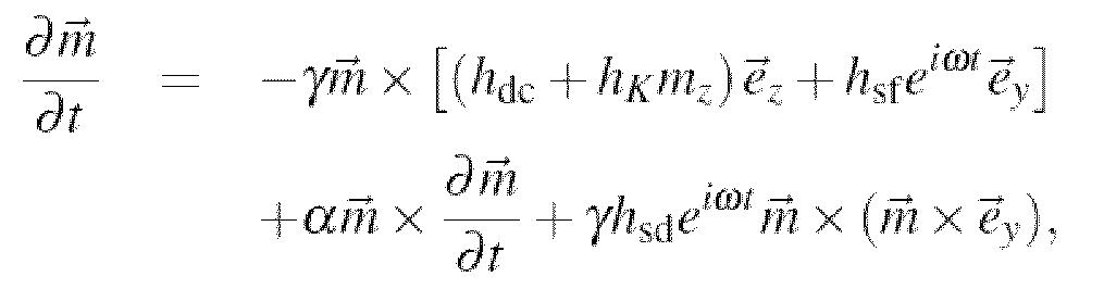
- the motion of magnetization is obtained by solving the motion equation (Landau-Lifshitz-Gilbert equation) of [Math. 7].
- ⁇ is the gyromagnetic ratio
- h dc is the external DC magnetic field applied in the z-direction
- h K is the effective magnetic field due to perpendicular magnetic anisotropy
- ⁇ is the Gilbert relaxation coefficient
- h sf e i ⁇ t and h sd e i ⁇ t are currents.
- the magnitude of the inductance is proportional to the cross-sectional area of the element in the prior art, whereas the magnitude of the inductance of the present invention is inversely proportional to the cross-sectional area of the element. Therefore, a smaller element with a smaller cross-sectional area provides a stronger inductance.
- This property is similar to the "emergent inductor utilizing a combination of spin transfer torque and its inverse process, spin electromotive force" proposed and demonstrated in Non-Patent Document 1.
- the first significance of the present invention is that this characteristic is realized by simple components. Furthermore, the realization of the variable inductance by the electric field has the second significance. As a method, there are two methods already explained.
- the first method modulates the magnitude of the spin-orbit interaction ⁇ R among the parameters of the above equation by an external electric field. Therefore, by applying an electric field to the inductor layer through the gate electrode, the magnitude of the inductance can be changed.
- FIG. 7 shows this situation.
- the second method is modulation of the inductance by the magnetic field. When an external magnetic field is applied in the film thickness direction of the element, the effective magnetic anisotropy of the equation changes. Through this action, the magnitude of the inductance can be changed by an external magnetic field.
- FIG. 8 shows this situation.
- a laminated film in which two different conductors are laminated and a pair of conductors arranged at both ends in a direction intersecting the laminating direction An element consisting of electrodes. This is because, as described in the section on suitable materials, a laminated film consisting of two layers of antiferromagnetic layer/antiferromagnetic layer is also included. It can be said that the element itself, which has such a laminated film and a pair of electrodes as the minimum elements, has never existed in the past.
- adding a gate electrode or a thin film coil to the element can also be broadly considered as a technical idea as a novel structure.
- the first layer which is a layer for generating spin-orbit torque when an alternating current is applied
- the first layer which is a layer for generating spin-orbit torque when an alternating current is applied
- an element consisting of a layer and a second layer which is the layer in which spin-orbit torque precesses the magnetic moment.
- an element in which a region for generating a local electric field is added to the first layer of the element and an element in which a coil for applying an external magnetic field is added to the element can be widely considered as a technical idea as a novel function. is.
- the inductance is proportionally increased. By doing so, it is also possible to increase the length l of the current path while keeping the element size small. If necessary measures are taken, such as specific aspects of multilayer wiring, magnetic dynamics control, and in particular countermeasures against interference through leakage fields between different magnetic layer magnetizations due to lamination, the perpendicular magnetization of the basic structure can be inter-layer coupled. However, the precession motion can be generated in the same phase as the alternating current, and in principle, the inductance can be increased.
- the thin film inductor element and the thin film variable inductor element according to the embodiments of the present invention have been described above in detail with reference to the drawings. Even if there is a change in design without departing from the gist of the invention, it is included in the present invention.
- the material and film thickness dimensions are limited to the examples disclosed here, it does not mean that the function of inductance will not be exhibited, but if the spin orbit torque can be exhibited (therefore, it is optimal for the expression of spin torque). (not that a certain material is essential).
- the exemplified materials are general materials for magnetic bodies, have effective magnetic anisotropy in a normal temperature range, and can control the change. Therefore, it is fully understood that the significance of the present invention is that it can provide an inductor element and a variable inductor element that can be used in a wide temperature range because they are less temperature dependent with common materials and simple structures. should be.
Landscapes
- Engineering & Computer Science (AREA)
- Power Engineering (AREA)
- Chemical & Material Sciences (AREA)
- Crystallography & Structural Chemistry (AREA)
- Microelectronics & Electronic Packaging (AREA)
- Thin Magnetic Films (AREA)
- Coils Or Transformers For Communication (AREA)
- Semiconductor Integrated Circuits (AREA)
- Hall/Mr Elements (AREA)
Abstract
Description
こうした中、電気機器や電気回路の小型化に必要なインダクタ素子の微細化に寄与するとの期待の下、近年、スピントロニクス技術に基づく創発電磁場によるインダクタ素子としての創発インダクタ(Emergent Inductor)の原理が解明され、実証にも成功している。非特許文献1で開示される創発インダクタ(Emergent Inductor)は、従前からのインダクションコイルとの対比説明である図9が示すように、インダクタンス強さと小型化というトレードオフの関係を持たず、むしろ逆に、素子断面積がインダクタンスに反比例し、小型化する程にインダクタンスが大きくなるという性質を有する。このため、創発インダクタはダウンサイジングに大きく貢献するものと期待されている。
本発明は、これらの課題を解決するべく、材料を選ぶ困難性が然程に高くなく、かつ、温度依存性も然程には高くない新しいタイプの創発電磁場を利用した薄膜インダクタ素子を提供することを発明の課題とするものである。
磁性体層と、非磁性体層又は反強磁性体層と、が積層された積層膜と、一対の電極を備え、前記磁性体層と前記非磁性体層又は前記反強磁性体層は、積層方向と直交する方向で任意の形状で延伸され、かつ、前記積層方向の上下向きも任意であり、前記磁性体層は、略一様な磁化構造を有しており、前記一対の電極は、前記積層膜が延伸される両端に設けられ、交流電流ないしは高周波電流が印加されることを特徴とする。
また、本発明の薄膜可変インダクタ素子は、少なくとも以下の構成を具備するものである。
磁性体層と、非磁性体層又は反強磁性体層と、が積層された積層膜と、障壁層と、交流電流ないしは高周波電流印加用の一対の電極と、ゲート電極層を備え、前記磁性体層と前記非磁性体層又は前記反強磁性体層は、積層方向と直交する方向で任意の形状で延伸され、かつ、前記積層方向の上下向きも任意であり、前記磁性体層は、略一様な磁化構造を有しており、前記一対の電極は、前記積層膜が延伸される両端に設けられ、交流電流ないしは高周波電流が印加され、前記障壁層は、前記非磁性体層又は前記反強磁性体層側の面にさらに積層されるようにして設けられ、前記ゲート電極層は、前記障壁層にさらに積層されるようにして設けられ、前記ゲート電極層に正負のバイアスを印加することによってインダクタンス変調動作が実現されることを特徴とする。
さらに、本発明の薄膜可変インダクタ素子は、少なくとも以下の構成を具備するものである。
磁性体層と、非磁性体層又は反強磁性体層と、が積層された積層膜と、交流電流ないしは高周波電流印加用の一対の電極と、前記積層膜を取り囲む薄膜コイルを備え、前記磁性体層と前記非磁性体層又は前記反強磁性体層は、積層方向と直交する方向で任意の形状で延伸され、かつ、前記積層方向の上下向きも任意であり、前記磁性体層は、略一様な磁化構造を有しており、前記薄膜コイルのオンオフ及び/又は電流の向きを切り替えて外部磁場を制御することによってインダクタンス変調動作が実現されることを特徴とする。
これらの発明において共通することとして、「積層膜」とは、磁性体層と、非磁性体層又は反強磁性体層とから成る二層膜を当然に含むことに加えて、下地層やギャップ層等の付加的な膜が加えられたものも含むものである。また、「任意の形状」とは、正方形、円、楕円、長方形など、どのような形状であっても良いという意味であるが、任意の形状を選択してもインダクタンスが発現されるということを意図している。また、「一対の電極は、前記積層膜が延伸される両端に設けられ」ということは、電極が設けられる積層方向での高さ位置は問われないものであるし、かつ、個々の電極どうしの高さ位置が揃っていない態様をも含むことを意図している。さらに、「略一様な磁化構造」とは、非特許文献1にて創発的なインダクタンスが実現される必須要件となっている螺旋磁気構造や横型コニカル磁気構造といった非共線的な磁気構造ではなく、隣り合う磁気モーメントが共線的に配列した磁気構造を意味するものであり、温度や材料の不完全性に起因した若干の非一様性も含むものである。
図1は、本発明の実施形態に係る薄膜インダクタ素子の構造概念を示す斜視図、断面図及び平面図である。磁性体層に重金属層を積層させた積層膜でインダクタが形成されている。x方向に延伸され、その両端には図示されない電極が設けられ、交流電流ないし高周波電流が印加される。電極の設けられるz位置は、重金属層寄り、磁性体層寄り、両者の境界近辺の任意の位置とすることができる。また、重金属層と磁性体層の上下関係も任意であり、図示のものと上下位置を入れ替えてもインダクタとして同条件で機能するものである。ただし、後記する薄膜可変インダクタ素子との共通モジュール化などを考慮したならば、図示された上下関係とするのが有利である。磁性体の磁化の方向は、図1の白抜き矢印が示すように、積層方向に平行な方向に安定した磁気異方性を有している。ただし、この磁気異方性は、飽くまで実施形態について説明したものであって、既に説明したように、略一様な磁化構造が形成されていれば、インダクタンスは発現される。なお、実際には磁化の方向は図中のz方向、またはx方向に平行方向を向くときに大きなインダクタンスが得られる。また、重金属層に限定されることなく、スピン軌道トルクを発現できる非磁性体層であれば、インダクタンスは発現される。言うまでもないことであるが、磁気抵抗メモリの磁性反転動作に要求されるところの外部磁場は必要とされない。
薄膜の堆積方法には超高真空スパッタリング法などを用いる。薄膜堆積後、磁場中にて熱処理を行っても良く、本実施形態に係る薄膜インダクタ素子では、300℃の雰囲気で2時間の処理を行った。
ここで、本発明の実施形態に係る薄膜インダクタ素子のインダクタ動作の原理を、図2を用いて、説明する。インダクタ動作は、スピントルク過程とスピン起電力過程が交互に生じることにより実現される。何らかの原因によって誘導電流が発生する場合に電流の流れる方向が誘導電流の原因を妨げる方向と一致するという電磁誘導についてのレンツの法則のスピントロニクス版であると捉えると理解がし易い。以下、具体的に説明する。
以上のことから理解されるように、重金属層(或いは広く一般に非磁性体層)については、磁性体層にスピン軌道トルクを及ぼすことが絶対的に必要な条件となる。この元素としては、W, Ta, Pd, Pt, Irが知られており、これらから選択するのが好適である。
二層膜の各膜の形状は同一形状とすれば、積層膜の平面形状としては、正方形、円、楕円、長方形などの任意の形状を選択しても、インダクタンスを発現できる。ただし、現実的な取り扱いを考えれば、長方形を選択するのが有利であろう。
なお図ではインダクタ素子は磁性体層と重金属層の二層から構成されるものとして示されているが、実際には製造の過程でこれらの層を所望の特性が得られるように形成するための下地層や、微細加工の過程で素子を保護するためのキャップ層などが設けられた積層膜であっても良い。
本発明の実施形態として、以下の4つの積層構成を用いて実験を行い、素子サイズを長さ100μm、幅100nm、厚み10nmに規格化した場合のインダクタンスを求めた。
1つ目は、基板側からSi sub./ Ta(3)/ CoFeB(1)/ MgO(1.3)/ Ta(1)なる膜構成とした。この場合に生成される電流密度当たりのスピン軌道トルク有効磁場の大きさは1.1x10⁻¹¹ [mT/(A/m2)]であり、この場合のインダクタンスは0.0065 [nH]となった。
2つ目は、基板側からSi sub./ W(3)/ CoFeB (1.3)/ MgO(1.3)/ Ta(1)なる膜構成とした。この場合に生成される電流密度当たりのスピン軌道トルク有効磁場の大きさは9.0x10⁻¹¹ [mT/(A/m2)]であり、この場合のインダクタンスは1.0 [nH]となった。
3つ目は、基板側からSi sub./ Ta(2)/ Pt(3)/ Co(1.6)/ MgO(2)/ Ta(1)なる膜構成とした。この場合に生成される電流密度当たりのスピン軌道トルク有効磁場の大きさは1.4x10⁻¹¹ [mT/(A/m2)]であり、この場合のインダクタンスは0.04 [nH]となった。
4つ目は、基板側からSi sub./ Ta(4)/ Pt(2)/ PtMn(3)/ [Co(0.3)/Ni(0.6)]2/ Co(0.3)/ MgO(1.5)/ Ru(1)なる膜構成とした。この場合に生成される電流密度当たりのスピン軌道トルク有効磁場の大きさは4.2x10⁻¹¹ [mT/(A/m2)]であり、この場合のインダクタンスは0.1 [nH]となった。
古典電磁気学の原理を用い、同じサイズのインダクタを空芯のソレノイドコイルで製造する場合のインダクタンスは以下のように見積もられる。
インダクタの長さ100μm、幅100nm、厚み10nmと仮定し、ソレノイドコイルの巻き密度については現行の微細加工技術で実現可能な値として100nmあたり1周と仮定する。ソレノイドコイルのインダクタンスLは透磁率をμ0、巻き密度をn、長さをl、幅をW、厚みをtとするとL = μ0n2lWt で与えられ、0.013 nHと求まる。ただし、本発明の原理に基づくインダクタ素子は積層膜を細線状に加工するのみで実現できることから、古典的なインダクタと比べると製造コストは格段に抑えられる。すなわち、本発明の実施形態に係る薄膜インダクタ素子は、従来の古典的なインダクタと比べ、圧倒的に低いコストで同等かそれを大きく上回るインダクタンスを実現可能である。
これに対して、本発明の実施形態に係る薄膜インダクタ素子では、そもそも共線的な磁気構造を有する標準的な磁性体を用いれば足りる。その上、二重膜の構造から磁化の容易軸が膜面垂直に決まっており、単純な成膜で素子作製ができるものであり、圧倒的に低いコストでインダクタンスを実現可能である。
これに対して、本発明の実施形態に係る薄膜インダクタ素子では、Ni-Fe合金、Co-Fe-B合金、Co/Ni, Co/Pt, Co/Pd, Co/Au, Fe/Au積層膜, Co-Pt, Co-Cr-Pt, Co-Pd, Fe-Pt, Fe-Pd, Fe-Co-Pt, Fe-Co-Pd合金、CoFeB, FeB合金といった一般的な材料を使用できるものであり、これらは通常温度で十分に機能するものである。したがって、本発明の実施形態に係る薄膜インダクタ素子は、実用化に向けての障害は低いものである。
本発明の原理によるインダクタ素子については、インダクタンスを外部から制御できることも判明している。このことにより、インダクタンスを可変とする薄膜可変インダクタ素子を実現することが可能である。図3は、本発明の実施形態に係る薄膜可変インダクタ素子の構造概念を示す斜視図、断面図及び平面図である。磁性体層に重金属層を積層させた二層膜でインダクタが形成され、x方向に延伸され、その両端には図示されない電極が設けられ、交流電流が印加される点は、図1に示される薄膜インダクタ素子と同様である。電極の設けられる箇所や、二層膜の形状についても、薄膜インダクタ素子と同様に自由度が高い。
一方、薄膜可変インダクタ素子では、二層膜の重金属層の面に隣接して、絶縁体から構成される障壁層が積層されている。材料としては、MgO, Al2O3, AlNなどが挙げられるが、障壁層と記録層の間の界面磁気異方性により垂直磁気異方性を発現することが重要であり、この観点ではCoFeB/MgO, FeB/MgOが好適である。ただし上述のように、薄膜可変インダクタ素子の場合も、その磁化容易軸の方向には任意性があり、例えばx方向を向いていても良い。
そして、障壁層の上には、金属から構成されるゲート電極層がさらに積層されている。材料としては、伝導性のよい金属、例えば、Ta, Ru, Cuなどが好適である。ゲート電極層の形状として、x-y平面内で障壁層の内側に収めるように設定されている。これは、ゲート電極層をインダクタと電気的に短絡させないためである。一方で、二層膜の平面形状としては、正方形、円、楕円、長方形などの任意の形状を選択できることは、薄膜インダクタ素子と同様である。
磁性体の磁化の方向は、図3の白抜き矢印が示すように、積層方向に平行な方向に安定した磁気異方性を有している。ただし、この磁気異方性は、飽くまで実施形態について説明したものであって、略一様な磁化構造が形成されていれば、インダクタンスは発現される。また、重金属層に限定されることなく、スピン軌道トルクを発現できる非磁性体層であれば、インダクタンスは発現される。言うまでもないことであるが、磁気抵抗メモリの磁性反転動作に要求されるところの外部磁場は必要とされない。
本発明の実施形態に係る薄膜可変インダクタ素子のインダクタンス変調動作の原理を、図4を用いて、説明する。
ゲート電極層に正バイアスを印加すると、インダクタの絶縁層との接合面境界に電子が蓄積し、C-MOSのゲート下のチャネル領域の如く局所電界が生じる。電界効果によりインダクタに働くスピン軌道相互作用が変化し、インダクタンスの決定要因である種々の因子が変調される。因子としては、スピン軌道トルクの大きさ、その逆過程であるスピン起電力の大きさ、磁化方向の変化しやすさを支配する磁気異方性の大きさが挙げられる。これら因子の変調作用の結果として、二層膜境界に発生するインダクタンスが変調されることになる。
ゲート電極層に負バイアスを印加すると、インダクタの絶縁層との接合面境界に正孔が蓄積し、前記とは逆の局所電界が生じる。電界効果によるスピン軌道相互作用の変化は、電界に比例する成分と電界の二乗に比例する成分がある。このため必ずしも正バイアス時と負バイアス時で逆向きの変調作用を常時期待することはできないが、多くの重金属で電界に比例する効果が確認されており、適切な材料選択により双方向性のインダクタンス変調動作が実現可能となる。
古典電磁気学の原理を用いたインダクタにおいて、インダクタンス変調ができるものが知られている。しかし、そのためには、透磁率を高めるためのコアを可動させるといった機械的な部品が必要となる。この点、本発明の実施形態に係る薄膜可変インダクタ素子は、バイアス存在下でインダクタンス動作を行うことで、機械動作を伴わない電気的な制御による高速可変インダクタンスが実現できる。
一方、スピン移行トルク(STT: Spin-transfer torque)とその逆過程であるスピン起電力の組み合わせを利用する創発インダクタに目を向けた場合、温度と磁界によるインダクタンス変化は観測されているものの、数テスラという大きな磁界が必要であるなど、制御に伴う困難性が著しく高いものである。加えて、温度変化が大きすぎる点は制御を行う上ではデメリットですらある。この点、単純な金属二層膜を利用した本発明の実施形態に係る薄膜可変インダクタ素子は、温度変化が少なく、電流パスと直交する電界で制御できるものであり、制御性は極めて高いものとなる。
図3の実施例は、ゲート電極下に電荷を集めることにより生じる局所電界でインダクタンスの諸因子延いてはインダクタンスを変調させるものであったが、外部磁場を与えることで磁性体の揺れ易さ(運動のし易さ)を制御することによってインダクタンスを変調させることもできる。
図5は、外部磁場を与えることによって機能する薄膜可変インダクタ素子の構造概念を示す斜視図、断面図及び平面図である。磁性体層に重金属層を積層させた二層膜でインダクタが形成され、x方向に延伸され、その両端には図示されない電極が設けられ、交流電流が印加される点は、図3に示される薄膜可変インダクタ素子と同様である。電極の設けられる箇所や、二層膜の形状についても、図3に示される薄膜可変インダクタ素子と同様に自由度が高い。すなわち、二層膜の平面形状としては、正方形、円、楕円、長方形などの任意の形状を選択できる。
磁性体の磁化の方向は、図5の白抜き矢印が示すように、積層方向に平行な方向に安定した磁気異方性を有している。ただし、この磁気異方性は、飽くまで実施形態について説明したものであって、略一様な磁化構造が形成されていれば、インダクタンスは発現される。また、重金属層に限定されることなく、スピン軌道トルクを発現できる非磁性体層であれば、インダクタンスは発現される。
図3に示される薄膜可変インダクタ素子と相違する点は、ゲート電極の代わりに、積層膜を取り囲む薄膜コイルを備えている点である。当該薄膜コイルを制御する回路により、電流のオンオフや電流の向きを切り替えることによってインダクタ素子を積層方向に貫くエルステッド磁場を制御できるようにされている。
外部磁場を与えることによって機能する薄膜可変インダクタ素子のインダクタンス変調動作の原理を、図6を用いて、説明する。
制御回路にて+z方向に正磁界を印加すると、インダクタの磁性体における有効磁気異方性が増大(磁性体の揺れ易さは減少)し、インダクタンスが減少する。反対に負磁界を印加すると、インダクタの磁性体における有効磁気異方性が減少(磁性体の揺れ易さは増大)し、インダクタンスが増大する。従って、制御電流によって発生させた外部磁界を印加しながら前記インダクタンス動作を行うことで、従来技術のような機械動作を伴わない電気的な制御による可変インダクタンスが実現できる。なお、ここでは磁性体の磁化容易軸の方向がz方向にある場合を仮定して原理の説明を行ったが、磁性体の磁化容易軸方向が変わった場合には印加する磁界の方向もそれに応じて変わり得る。
ここで、局所電界による薄膜可変インダクタ素子及び外部磁場による薄膜可変インダクタ素子に共通する有利な効果について述べると、使用周波数帯域が広範であるという点が挙げられる。スピン移行トルクを用いる先行研究の創発インダクタは、非特許文献1によれば、30kHz以上の周波数でインダクタンスは急速に減少することが判明している。この使用限界周波数は、螺旋磁性の並進運動を妨げる局所的な乱れによって規定され、改良を重ねたとしても、例えばGHz帯で使えるようにするのは非常に困難であると思われる。これに対して、本発明は、螺旋磁性のような磁気の空間パターンの並進運動を用いることなく、一様な磁気歳差運動を使うため、素子の乱れが直接関与することがない。結果として、本発明であれば数Hzから数GHzまでといった超広範囲のレンジで一定のインダクタンスを提供することが可能となる。この点は、高周波用途としては重要なことである。
これまでに説明した事象の基礎となる動作原理を説明する。動作原理は、以下に説明する導出過程により得られる公式として説明することができる。
ラシュバスピン軌道結合(Rashba spin-orbit coupling:以下、「RSOC」という。)は、反転対称性の破れた材料系、例えば重金属と異種材料との界面等で生じ、スピン軌道トルクやスピン起電力など電子スピンの制御手段をもたらすことが知られている。特に磁性体と重金属の界面においては、伝導電子はRSOC のもとで以下のような有効的な電場(スピン電場)を感じることが知られている。


磁化はz方向まわりの小角歳差運動を行うと仮定する。すなわち、[数3]で表される。



磁化の運動は、[数7]の運動方程式(Landau-Lifshitz-Gilbert 方程式)を解くことによって得られる。
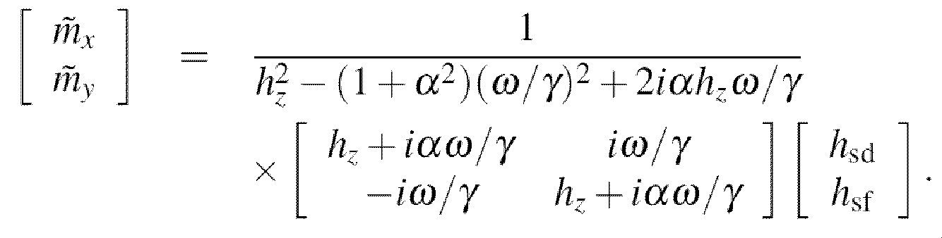
[数8]を[数6]に代入することにより、創発インダクタンスLの公式である[数9]が得られる。
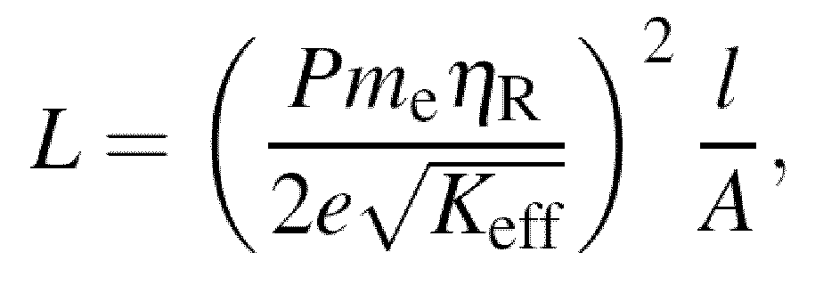
さらに、電界による可変インダクタンスを実現したことに第二の意義がある。方式としては既に説明した2つの方式がある。一つ目の方式は、上で述べた式のパラメーターの内、スピン軌道相互作用の大きさηRを外部電界によって変調するものである。このため、ゲート電極によってインダクタ層に電界を印加することで、インダクタンスの大きさを変化させることができる。この様子を示したのが、図7である。
二つ目の方式は、磁界によるインダクタンスの変調である。外部磁界を素子の膜厚方向に印加すると、式の実効的な磁気異方性が変化する。この作用を通じて、外部磁界によって、インダクタンスの大きさを変化させることができる。この様子を示したのが、図8である。
ここで説明された特徴から把握される技術的思想を構造として最も上位のものとして観念すれば、二つの異なる導体が積層された積層膜と、積層方向に交わる方向の両端に配置される一対の電極から成る素子ということになる。好適となる材料の項で説明したように、反強磁性体層/反強磁性体層の二層から成る積層膜も含まれるからである。このような積層膜と一対の電極を最小要素とする素子自体、従来には全くなかった素子といえる。加えて、当該素子に、ゲート電極又は薄膜コイルを付加したものも、新規な構造としての技術的思想として広く観念できるものである。
また、ここで説明された特徴から把握される技術的思想を機能として最も上位のものとして観念すれば、交番電流が与えられたときに、スピン軌道トルクを生成するための層である第1の層と、スピン軌道トルクによって磁気モーメントの歳差運動が生じる層である第2の層から成る素子ということになる。加えて、当該素子の第1の層に局所電界を生じさせる領域を付加した素子と、当該素子に外部磁場を与えるコイルを付加した素子も、新規な機能としての技術的思想として広く観念できるものである。
さらに、実施形態としての説明は行わなかったが、[数9]右辺の長さlに着目して技術的思想を拡張することも可能である。すなわち、素子の長手方向の長さlが延長されればそれに比例してインダクタンスは強くなるところ、例えば、「フィルムコンデンサ」のような形で、本発明の素子の基本構造を巻回するか積層することによって、素子サイズを小さく保ったままで電流パスの長さlを増大することも可能である。多層膜の配線の具体的態様や、磁気ダイナミクス制御、特に積層による異なる磁性層磁化間の漏れ磁場を介した干渉への対処といった必要な措置を講じれば、基本構造の膜面垂直磁化が層間結合し交流電流と同位相での歳差運動を生じさせることができ、原理的にインダクタンスの増強が可能である。
特に、材料や膜厚寸法などは、ここで開示された例に限定されなければ、インダクタンスの機能が発現されないというものではなく、スピン軌道トルクの発現ができれば(したがって、スピントルクの発現に最適である材料が必須というものでもない)利用可能なものとなる。
例示された材料は、磁性体の材料として一般的なものであり、通常の温度範囲で実効的な磁気異方性を有し、また、その変化を制御し得るものである。したがって、一般的な材料と簡易な構造によって、温度依存性が少ないことから、広い温度範囲で使用できるインダクタ素子及び可変インダクタ素子を提供できることに、本発明の意義があることは十分に理解されるべきものである。
Claims (8)
- 磁性体層と、非磁性体層又は反強磁性体層と、が積層された積層膜と、一対の電極を備え、
前記磁性体層と前記非磁性体層又は前記反強磁性体層は、積層方向と直交する方向で任意の形状で延伸され、かつ、前記積層方向の上下向きも任意であり、
前記磁性体層は、略一様な磁化構造を有しており、
前記一対の電極は、前記積層膜が延伸される両端に設けられ、交流電流ないしは高周波電流が印加される
ことを特徴とする薄膜インダクタ素子。 - 前記非磁性体層は、スピン軌道トルクの発現に適した組成である
ことを特徴とする請求項1に記載の薄膜インダクタ素子。 - 前記スピン軌道トルクの発現に適した組成は、W, Ta, Pd, Pt, Irの元素から選択される重金属を含む
ことを特徴とする請求項2に記載の薄膜インダクタ素子。 - 前記反磁性体層は、スピン軌道トルクの発現に適した組成である
ことを特徴とする請求項1に記載の薄膜インダクタ素子。 - 前記スピン軌道トルクの発現に適した組成は、Cr, Mn, Fe, Co, Niからなる群より選ばれる第一の元素とRu, Rh, Pd, Ag, Os, Ir, Pt, Auからなる群より選ばれる第二の元素を含む合金である
ことを特徴とする請求項4に記載の薄膜インダクタ素子。 - 磁性体層と、非磁性体層又は反強磁性体層と、が積層された積層膜と、障壁層と、交流電流ないしは高周波電流印加用の一対の電極と、ゲート電極層を備え、
前記磁性体層と前記非磁性体層又は前記反強磁性体層は、積層方向と直交する方向で任意の形状で延伸され、かつ、前記積層方向の上下向きも任意であり、
前記磁性体層は、略一様な磁化構造を有しており、
前記一対の電極は、前記積層膜が延伸される両端に設けられ、交流電流ないしは高周波電流が印加され、
前記障壁層は、前記非磁性体層又は前記反強磁性体層側の面にさらに積層されるようにして設けられ、
前記ゲート電極層は、前記障壁層にさらに積層されるようにして設けられ、
前記ゲート電極層に正負のバイアスを印加することによってインダクタンス変調動作が実現される
ことを特徴とする薄膜可変インダクタ素子。 - 前記ゲート電極層は、前記積層方向に平行な面内において前記障壁層よりも小さい形状とされている
ことを特徴とする請求項6に記載の薄膜可変インダクタ素子。 - 磁性体層と、非磁性体層又は反強磁性体層と、が積層された積層膜と、交流電流ないしは高周波電流印加用の一対の電極と、前記積層膜を取り囲む薄膜コイルを備え、
前記磁性体層と前記非磁性体層又は前記反強磁性体層は、積層方向と直交する方向で任意の形状で延伸され、かつ、前記積層方向の上下向きも任意であり、
前記磁性体層は、略一様な磁化構造を有しており、
前記薄膜コイルのオンオフ及び/又は電流の向きを切り替えて外部磁場を制御することによってインダクタンス変調動作が実現される
ことを特徴とする薄膜可変インダクタ素子。
Priority Applications (3)
| Application Number | Priority Date | Filing Date | Title |
|---|---|---|---|
| US18/546,002 US20240145147A1 (en) | 2021-02-26 | 2022-01-07 | Thin film inductor element and thin film variable inductor element |
| CN202280014817.7A CN116848601A (zh) | 2021-02-26 | 2022-01-07 | 薄膜电感元件及薄膜可变电感元件 |
| KR1020237027254A KR102897137B1 (ko) | 2021-02-26 | 2022-01-07 | 박막 인덕터 소자 및 박막 가변 인덕터 소자 |
Applications Claiming Priority (2)
| Application Number | Priority Date | Filing Date | Title |
|---|---|---|---|
| JP2021030176A JP7580068B2 (ja) | 2021-02-26 | 2021-02-26 | 薄膜インダクタ素子及び薄膜可変インダクタ素子 |
| JP2021-030176 | 2021-02-26 |
Publications (1)
| Publication Number | Publication Date |
|---|---|
| WO2022181069A1 true WO2022181069A1 (ja) | 2022-09-01 |
Family
ID=83048864
Family Applications (1)
| Application Number | Title | Priority Date | Filing Date |
|---|---|---|---|
| PCT/JP2022/000296 Ceased WO2022181069A1 (ja) | 2021-02-26 | 2022-01-07 | 薄膜インダクタ素子及び薄膜可変インダクタ素子 |
Country Status (6)
| Country | Link |
|---|---|
| US (1) | US20240145147A1 (ja) |
| JP (1) | JP7580068B2 (ja) |
| KR (1) | KR102897137B1 (ja) |
| CN (1) | CN116848601A (ja) |
| TW (1) | TWI906482B (ja) |
| WO (1) | WO2022181069A1 (ja) |
Cited By (5)
| Publication number | Priority date | Publication date | Assignee | Title |
|---|---|---|---|---|
| WO2025009154A1 (ja) * | 2023-07-06 | 2025-01-09 | Tdk株式会社 | スピンインダクタ |
| WO2025009050A1 (ja) | 2023-07-04 | 2025-01-09 | Tdk株式会社 | スピンインダクタ |
| WO2025009065A1 (ja) * | 2023-07-04 | 2025-01-09 | Tdk株式会社 | スピンインダクタ及びスピンインダクタデバイスの製造方法 |
| WO2026033583A1 (ja) * | 2024-08-05 | 2026-02-12 | Tdk株式会社 | スピンインダクタ |
| WO2026033584A1 (ja) * | 2024-08-05 | 2026-02-12 | Tdk株式会社 | スピンインダクタ |
Families Citing this family (4)
| Publication number | Priority date | Publication date | Assignee | Title |
|---|---|---|---|---|
| JP2024017023A (ja) * | 2022-07-27 | 2024-02-08 | 慶應義塾 | 磁気センサ、及び磁性薄膜チップ |
| CN118120034A (zh) * | 2022-09-30 | 2024-05-31 | Tdk株式会社 | 自旋电感器 |
| JP7878655B2 (ja) * | 2022-11-16 | 2026-06-23 | 国立研究開発法人日本原子力研究開発機構 | 薄膜インダクタ素子、薄膜可変インダクタ素子及び積層薄膜素子の使用方法 |
| CN118841235B (zh) * | 2024-07-11 | 2025-05-06 | 南京大学 | 无线圈式质子型电感器、设计方法及调控方法 |
Citations (2)
| Publication number | Priority date | Publication date | Assignee | Title |
|---|---|---|---|---|
| JP2002158112A (ja) * | 2000-09-12 | 2002-05-31 | Memscap | 微小インダクタや微小変圧器といったタイプの微小素子 |
| US20100194510A1 (en) * | 2009-02-02 | 2010-08-05 | Klemens Pruegl | Inductive Electrical Device |
Family Cites Families (2)
| Publication number | Priority date | Publication date | Assignee | Title |
|---|---|---|---|---|
| KR101598295B1 (ko) * | 2014-09-22 | 2016-02-26 | 삼성전기주식회사 | 다층 시드 패턴 인덕터, 그 제조방법 및 그 실장 기판 |
| EP3832676B1 (en) * | 2018-08-01 | 2025-04-23 | Riken | Inductor element and apparatus including same |
-
2021
- 2021-02-26 JP JP2021030176A patent/JP7580068B2/ja active Active
-
2022
- 2022-01-07 CN CN202280014817.7A patent/CN116848601A/zh active Pending
- 2022-01-07 WO PCT/JP2022/000296 patent/WO2022181069A1/ja not_active Ceased
- 2022-01-07 KR KR1020237027254A patent/KR102897137B1/ko active Active
- 2022-01-07 US US18/546,002 patent/US20240145147A1/en active Pending
- 2022-02-24 TW TW111106822A patent/TWI906482B/zh active
Patent Citations (2)
| Publication number | Priority date | Publication date | Assignee | Title |
|---|---|---|---|---|
| JP2002158112A (ja) * | 2000-09-12 | 2002-05-31 | Memscap | 微小インダクタや微小変圧器といったタイプの微小素子 |
| US20100194510A1 (en) * | 2009-02-02 | 2010-08-05 | Klemens Pruegl | Inductive Electrical Device |
Cited By (5)
| Publication number | Priority date | Publication date | Assignee | Title |
|---|---|---|---|---|
| WO2025009050A1 (ja) | 2023-07-04 | 2025-01-09 | Tdk株式会社 | スピンインダクタ |
| WO2025009065A1 (ja) * | 2023-07-04 | 2025-01-09 | Tdk株式会社 | スピンインダクタ及びスピンインダクタデバイスの製造方法 |
| WO2025009154A1 (ja) * | 2023-07-06 | 2025-01-09 | Tdk株式会社 | スピンインダクタ |
| WO2026033583A1 (ja) * | 2024-08-05 | 2026-02-12 | Tdk株式会社 | スピンインダクタ |
| WO2026033584A1 (ja) * | 2024-08-05 | 2026-02-12 | Tdk株式会社 | スピンインダクタ |
Also Published As
| Publication number | Publication date |
|---|---|
| JP2022131304A (ja) | 2022-09-07 |
| CN116848601A (zh) | 2023-10-03 |
| KR20230149810A (ko) | 2023-10-27 |
| TW202240610A (zh) | 2022-10-16 |
| KR102897137B1 (ko) | 2025-12-09 |
| TWI906482B (zh) | 2025-12-01 |
| JP7580068B2 (ja) | 2024-11-11 |
| US20240145147A1 (en) | 2024-05-02 |
Similar Documents
| Publication | Publication Date | Title |
|---|---|---|
| JP7580068B2 (ja) | 薄膜インダクタ素子及び薄膜可変インダクタ素子 | |
| US20160211317A1 (en) | Systems and Methods for Integrated Multi-Layer Magnetic Films | |
| US20250253234A1 (en) | Magnetic core with hard ferromagnetic biasing layers and structures containing same | |
| WO2024069926A1 (ja) | スピンインダクタ | |
| TW202414452A (zh) | 自旋電感器 | |
| TW202025528A (zh) | 電場控制奈米磁鐵及包含其的自旋軌道耦合力矩磁阻式隨機存取記憶體 | |
| US20260143725A1 (en) | Magnetic thin film inductor structures | |
| Łazarski et al. | Spin-orbit torque induced magnetization dynamics and switching in a CoFeB/Ta/CoFeB system with mixed magnetic anisotropy | |
| JP2001339110A (ja) | 磁気制御素子とそれを用いた磁気部品及びメモリー装置 | |
| JP2016537827A (ja) | 磁気強化型エネルギー貯蔵システムおよび方法 | |
| WO2020090719A1 (ja) | スピントルク発生素子、その製造方法、及び、磁化制御装置 | |
| US9728321B2 (en) | Transformer with ferromagnetic foil windings | |
| US20100194510A1 (en) | Inductive Electrical Device | |
| WO2024105907A1 (ja) | 薄膜インダクタ素子、薄膜可変インダクタ素子及び積層薄膜素子の使用方法 | |
| CN121753121A (zh) | 自旋电感器 | |
| WO2026033584A1 (ja) | スピンインダクタ | |
| JP2019096800A (ja) | 3端子素子 | |
| WO2026033583A1 (ja) | スピンインダクタ | |
| JP2020047965A (ja) | 共振器 | |
| JPH05275254A (ja) | 平面型磁気素子 | |
| JPH05258980A (ja) | 平面型磁気素子 | |
| JP2001250718A (ja) | 傾斜機能多層膜磁性体 |
Legal Events
| Date | Code | Title | Description |
|---|---|---|---|
| 121 | Ep: the epo has been informed by wipo that ep was designated in this application |
Ref document number: 22759112 Country of ref document: EP Kind code of ref document: A1 |
|
| WWE | Wipo information: entry into national phase |
Ref document number: 18546002 Country of ref document: US |
|
| WWE | Wipo information: entry into national phase |
Ref document number: 202280014817.7 Country of ref document: CN |
|
| NENP | Non-entry into the national phase |
Ref country code: DE |
|
| 122 | Ep: pct application non-entry in european phase |
Ref document number: 22759112 Country of ref document: EP Kind code of ref document: A1 |