WO2022172349A1 - 化学結合法及びパッケージ型電子部品 - Google Patents
化学結合法及びパッケージ型電子部品 Download PDFInfo
- Publication number
- WO2022172349A1 WO2022172349A1 PCT/JP2021/004913 JP2021004913W WO2022172349A1 WO 2022172349 A1 WO2022172349 A1 WO 2022172349A1 JP 2021004913 W JP2021004913 W JP 2021004913W WO 2022172349 A1 WO2022172349 A1 WO 2022172349A1
- Authority
- WO
- WIPO (PCT)
- Prior art keywords
- bonding
- film
- thin film
- substrates
- package
- Prior art date
- Legal status (The legal status is an assumption and is not a legal conclusion. Google has not performed a legal analysis and makes no representation as to the accuracy of the status listed.)
- Ceased
Links
Images


Classifications
-
- C—CHEMISTRY; METALLURGY
- C23—COATING METALLIC MATERIAL; COATING MATERIAL WITH METALLIC MATERIAL; CHEMICAL SURFACE TREATMENT; DIFFUSION TREATMENT OF METALLIC MATERIAL; COATING BY VACUUM EVAPORATION, BY SPUTTERING, BY ION IMPLANTATION OR BY CHEMICAL VAPOUR DEPOSITION, IN GENERAL; INHIBITING CORROSION OF METALLIC MATERIAL OR INCRUSTATION IN GENERAL
- C23C—COATING METALLIC MATERIAL; COATING MATERIAL WITH METALLIC MATERIAL; SURFACE TREATMENT OF METALLIC MATERIAL BY DIFFUSION INTO THE SURFACE, BY CHEMICAL CONVERSION OR SUBSTITUTION; COATING BY VACUUM EVAPORATION, BY SPUTTERING, BY ION IMPLANTATION OR BY CHEMICAL VAPOUR DEPOSITION, IN GENERAL
- C23C14/00—Coating by vacuum evaporation, by sputtering or by ion implantation of the coating forming material
- C23C14/06—Coating by vacuum evaporation, by sputtering or by ion implantation of the coating forming material characterised by the coating material
- C23C14/08—Oxides
- C23C14/086—Oxides of zinc, germanium, cadmium, indium, tin, thallium or bismuth
-
- H—ELECTRICITY
- H10—SEMICONDUCTOR DEVICES; ELECTRIC SOLID-STATE DEVICES NOT OTHERWISE PROVIDED FOR
- H10W—GENERIC PACKAGES, INTERCONNECTIONS, CONNECTORS OR OTHER CONSTRUCTIONAL DETAILS OF DEVICES COVERED BY CLASS H10
- H10W74/00—Encapsulations, e.g. protective coatings
- H10W74/10—Encapsulations, e.g. protective coatings characterised by their shape or disposition
- H10W74/131—Encapsulations, e.g. protective coatings characterised by their shape or disposition the semiconductor body being only partially enclosed
- H10W74/137—Encapsulations, e.g. protective coatings characterised by their shape or disposition the semiconductor body being only partially enclosed the encapsulations being directly on the semiconductor body
-
- B—PERFORMING OPERATIONS; TRANSPORTING
- B23—MACHINE TOOLS; METAL-WORKING NOT OTHERWISE PROVIDED FOR
- B23K—SOLDERING OR UNSOLDERING; WELDING; CLADDING OR PLATING BY SOLDERING OR WELDING; CUTTING BY APPLYING HEAT LOCALLY, e.g. FLAME CUTTING; WORKING BY LASER BEAM
- B23K20/00—Non-electric welding by applying impact or other pressure, with or without the application of heat, e.g. cladding or plating
-
- C—CHEMISTRY; METALLURGY
- C23—COATING METALLIC MATERIAL; COATING MATERIAL WITH METALLIC MATERIAL; CHEMICAL SURFACE TREATMENT; DIFFUSION TREATMENT OF METALLIC MATERIAL; COATING BY VACUUM EVAPORATION, BY SPUTTERING, BY ION IMPLANTATION OR BY CHEMICAL VAPOUR DEPOSITION, IN GENERAL; INHIBITING CORROSION OF METALLIC MATERIAL OR INCRUSTATION IN GENERAL
- C23C—COATING METALLIC MATERIAL; COATING MATERIAL WITH METALLIC MATERIAL; SURFACE TREATMENT OF METALLIC MATERIAL BY DIFFUSION INTO THE SURFACE, BY CHEMICAL CONVERSION OR SUBSTITUTION; COATING BY VACUUM EVAPORATION, BY SPUTTERING, BY ION IMPLANTATION OR BY CHEMICAL VAPOUR DEPOSITION, IN GENERAL
- C23C14/00—Coating by vacuum evaporation, by sputtering or by ion implantation of the coating forming material
- C23C14/06—Coating by vacuum evaporation, by sputtering or by ion implantation of the coating forming material characterised by the coating material
- C23C14/08—Oxides
- C23C14/083—Oxides of refractory metals or yttrium
-
- C—CHEMISTRY; METALLURGY
- C23—COATING METALLIC MATERIAL; COATING MATERIAL WITH METALLIC MATERIAL; CHEMICAL SURFACE TREATMENT; DIFFUSION TREATMENT OF METALLIC MATERIAL; COATING BY VACUUM EVAPORATION, BY SPUTTERING, BY ION IMPLANTATION OR BY CHEMICAL VAPOUR DEPOSITION, IN GENERAL; INHIBITING CORROSION OF METALLIC MATERIAL OR INCRUSTATION IN GENERAL
- C23C—COATING METALLIC MATERIAL; COATING MATERIAL WITH METALLIC MATERIAL; SURFACE TREATMENT OF METALLIC MATERIAL BY DIFFUSION INTO THE SURFACE, BY CHEMICAL CONVERSION OR SUBSTITUTION; COATING BY VACUUM EVAPORATION, BY SPUTTERING, BY ION IMPLANTATION OR BY CHEMICAL VAPOUR DEPOSITION, IN GENERAL
- C23C14/00—Coating by vacuum evaporation, by sputtering or by ion implantation of the coating forming material
- C23C14/06—Coating by vacuum evaporation, by sputtering or by ion implantation of the coating forming material characterised by the coating material
- C23C14/10—Glass or silica
-
- C—CHEMISTRY; METALLURGY
- C23—COATING METALLIC MATERIAL; COATING MATERIAL WITH METALLIC MATERIAL; CHEMICAL SURFACE TREATMENT; DIFFUSION TREATMENT OF METALLIC MATERIAL; COATING BY VACUUM EVAPORATION, BY SPUTTERING, BY ION IMPLANTATION OR BY CHEMICAL VAPOUR DEPOSITION, IN GENERAL; INHIBITING CORROSION OF METALLIC MATERIAL OR INCRUSTATION IN GENERAL
- C23C—COATING METALLIC MATERIAL; COATING MATERIAL WITH METALLIC MATERIAL; SURFACE TREATMENT OF METALLIC MATERIAL BY DIFFUSION INTO THE SURFACE, BY CHEMICAL CONVERSION OR SUBSTITUTION; COATING BY VACUUM EVAPORATION, BY SPUTTERING, BY ION IMPLANTATION OR BY CHEMICAL VAPOUR DEPOSITION, IN GENERAL
- C23C14/00—Coating by vacuum evaporation, by sputtering or by ion implantation of the coating forming material
- C23C14/06—Coating by vacuum evaporation, by sputtering or by ion implantation of the coating forming material characterised by the coating material
- C23C14/14—Metallic material, boron or silicon
- C23C14/16—Metallic material, boron or silicon on metallic substrates or on substrates of boron or silicon
- C23C14/165—Metallic material, boron or silicon on metallic substrates or on substrates of boron or silicon by cathodic sputtering
-
- C—CHEMISTRY; METALLURGY
- C23—COATING METALLIC MATERIAL; COATING MATERIAL WITH METALLIC MATERIAL; CHEMICAL SURFACE TREATMENT; DIFFUSION TREATMENT OF METALLIC MATERIAL; COATING BY VACUUM EVAPORATION, BY SPUTTERING, BY ION IMPLANTATION OR BY CHEMICAL VAPOUR DEPOSITION, IN GENERAL; INHIBITING CORROSION OF METALLIC MATERIAL OR INCRUSTATION IN GENERAL
- C23C—COATING METALLIC MATERIAL; COATING MATERIAL WITH METALLIC MATERIAL; SURFACE TREATMENT OF METALLIC MATERIAL BY DIFFUSION INTO THE SURFACE, BY CHEMICAL CONVERSION OR SUBSTITUTION; COATING BY VACUUM EVAPORATION, BY SPUTTERING, BY ION IMPLANTATION OR BY CHEMICAL VAPOUR DEPOSITION, IN GENERAL
- C23C14/00—Coating by vacuum evaporation, by sputtering or by ion implantation of the coating forming material
- C23C14/22—Coating by vacuum evaporation, by sputtering or by ion implantation of the coating forming material characterised by the process of coating
- C23C14/34—Sputtering
- C23C14/3435—Applying energy to the substrate during sputtering
- C23C14/345—Applying energy to the substrate during sputtering using substrate bias
-
- C—CHEMISTRY; METALLURGY
- C23—COATING METALLIC MATERIAL; COATING MATERIAL WITH METALLIC MATERIAL; CHEMICAL SURFACE TREATMENT; DIFFUSION TREATMENT OF METALLIC MATERIAL; COATING BY VACUUM EVAPORATION, BY SPUTTERING, BY ION IMPLANTATION OR BY CHEMICAL VAPOUR DEPOSITION, IN GENERAL; INHIBITING CORROSION OF METALLIC MATERIAL OR INCRUSTATION IN GENERAL
- C23C—COATING METALLIC MATERIAL; COATING MATERIAL WITH METALLIC MATERIAL; SURFACE TREATMENT OF METALLIC MATERIAL BY DIFFUSION INTO THE SURFACE, BY CHEMICAL CONVERSION OR SUBSTITUTION; COATING BY VACUUM EVAPORATION, BY SPUTTERING, BY ION IMPLANTATION OR BY CHEMICAL VAPOUR DEPOSITION, IN GENERAL
- C23C14/00—Coating by vacuum evaporation, by sputtering or by ion implantation of the coating forming material
- C23C14/22—Coating by vacuum evaporation, by sputtering or by ion implantation of the coating forming material characterised by the process of coating
- C23C14/34—Sputtering
- C23C14/35—Sputtering by application of a magnetic field, e.g. magnetron sputtering
-
- C—CHEMISTRY; METALLURGY
- C23—COATING METALLIC MATERIAL; COATING MATERIAL WITH METALLIC MATERIAL; CHEMICAL SURFACE TREATMENT; DIFFUSION TREATMENT OF METALLIC MATERIAL; COATING BY VACUUM EVAPORATION, BY SPUTTERING, BY ION IMPLANTATION OR BY CHEMICAL VAPOUR DEPOSITION, IN GENERAL; INHIBITING CORROSION OF METALLIC MATERIAL OR INCRUSTATION IN GENERAL
- C23C—COATING METALLIC MATERIAL; COATING MATERIAL WITH METALLIC MATERIAL; SURFACE TREATMENT OF METALLIC MATERIAL BY DIFFUSION INTO THE SURFACE, BY CHEMICAL CONVERSION OR SUBSTITUTION; COATING BY VACUUM EVAPORATION, BY SPUTTERING, BY ION IMPLANTATION OR BY CHEMICAL VAPOUR DEPOSITION, IN GENERAL
- C23C14/00—Coating by vacuum evaporation, by sputtering or by ion implantation of the coating forming material
- C23C14/58—After-treatment
- C23C14/5846—Reactive treatment
- C23C14/5853—Oxidation
-
- H—ELECTRICITY
- H10—SEMICONDUCTOR DEVICES; ELECTRIC SOLID-STATE DEVICES NOT OTHERWISE PROVIDED FOR
- H10P—GENERIC PROCESSES OR APPARATUS FOR THE MANUFACTURE OR TREATMENT OF DEVICES COVERED BY CLASS H10
- H10P95/00—Generic processes or apparatus for manufacture or treatments not covered by the other groups of this subclass
-
- H—ELECTRICITY
- H10—SEMICONDUCTOR DEVICES; ELECTRIC SOLID-STATE DEVICES NOT OTHERWISE PROVIDED FOR
- H10W—GENERIC PACKAGES, INTERCONNECTIONS, CONNECTORS OR OTHER CONSTRUCTIONAL DETAILS OF DEVICES COVERED BY CLASS H10
- H10W72/00—Interconnections or connectors in packages
- H10W72/01—Manufacture or treatment
- H10W72/019—Manufacture or treatment of bond pads
-
- H—ELECTRICITY
- H10—SEMICONDUCTOR DEVICES; ELECTRIC SOLID-STATE DEVICES NOT OTHERWISE PROVIDED FOR
- H10W—GENERIC PACKAGES, INTERCONNECTIONS, CONNECTORS OR OTHER CONSTRUCTIONAL DETAILS OF DEVICES COVERED BY CLASS H10
- H10W72/00—Interconnections or connectors in packages
- H10W72/01—Manufacture or treatment
- H10W72/0198—Manufacture or treatment batch processes
-
- H—ELECTRICITY
- H10—SEMICONDUCTOR DEVICES; ELECTRIC SOLID-STATE DEVICES NOT OTHERWISE PROVIDED FOR
- H10W—GENERIC PACKAGES, INTERCONNECTIONS, CONNECTORS OR OTHER CONSTRUCTIONAL DETAILS OF DEVICES COVERED BY CLASS H10
- H10W72/00—Interconnections or connectors in packages
- H10W72/90—Bond pads, in general
-
- H—ELECTRICITY
- H10—SEMICONDUCTOR DEVICES; ELECTRIC SOLID-STATE DEVICES NOT OTHERWISE PROVIDED FOR
- H10W—GENERIC PACKAGES, INTERCONNECTIONS, CONNECTORS OR OTHER CONSTRUCTIONAL DETAILS OF DEVICES COVERED BY CLASS H10
- H10W76/00—Containers; Fillings or auxiliary members therefor; Seals
- H10W76/40—Fillings or auxiliary members in containers, e.g. centering rings
- H10W76/42—Fillings
- H10W76/43—Gaseous fillings
-
- H—ELECTRICITY
- H10—SEMICONDUCTOR DEVICES; ELECTRIC SOLID-STATE DEVICES NOT OTHERWISE PROVIDED FOR
- H10W—GENERIC PACKAGES, INTERCONNECTIONS, CONNECTORS OR OTHER CONSTRUCTIONAL DETAILS OF DEVICES COVERED BY CLASS H10
- H10W76/00—Containers; Fillings or auxiliary members therefor; Seals
- H10W76/60—Seals
-
- H—ELECTRICITY
- H10—SEMICONDUCTOR DEVICES; ELECTRIC SOLID-STATE DEVICES NOT OTHERWISE PROVIDED FOR
- H10W—GENERIC PACKAGES, INTERCONNECTIONS, CONNECTORS OR OTHER CONSTRUCTIONAL DETAILS OF DEVICES COVERED BY CLASS H10
- H10W95/00—Packaging processes not covered by the other groups of this subclass
-
- H—ELECTRICITY
- H10—SEMICONDUCTOR DEVICES; ELECTRIC SOLID-STATE DEVICES NOT OTHERWISE PROVIDED FOR
- H10W—GENERIC PACKAGES, INTERCONNECTIONS, CONNECTORS OR OTHER CONSTRUCTIONAL DETAILS OF DEVICES COVERED BY CLASS H10
- H10W99/00—Subject matter not provided for in other groups of this subclass
-
- H—ELECTRICITY
- H10—SEMICONDUCTOR DEVICES; ELECTRIC SOLID-STATE DEVICES NOT OTHERWISE PROVIDED FOR
- H10W—GENERIC PACKAGES, INTERCONNECTIONS, CONNECTORS OR OTHER CONSTRUCTIONAL DETAILS OF DEVICES COVERED BY CLASS H10
- H10W72/00—Interconnections or connectors in packages
- H10W72/01—Manufacture or treatment
- H10W72/019—Manufacture or treatment of bond pads
- H10W72/01931—Manufacture or treatment of bond pads using blanket deposition
- H10W72/01938—Manufacture or treatment of bond pads using blanket deposition in gaseous form, e.g. by CVD or PVD
-
- H—ELECTRICITY
- H10—SEMICONDUCTOR DEVICES; ELECTRIC SOLID-STATE DEVICES NOT OTHERWISE PROVIDED FOR
- H10W—GENERIC PACKAGES, INTERCONNECTIONS, CONNECTORS OR OTHER CONSTRUCTIONAL DETAILS OF DEVICES COVERED BY CLASS H10
- H10W72/00—Interconnections or connectors in packages
- H10W72/90—Bond pads, in general
- H10W72/951—Materials of bond pads
-
- H—ELECTRICITY
- H10—SEMICONDUCTOR DEVICES; ELECTRIC SOLID-STATE DEVICES NOT OTHERWISE PROVIDED FOR
- H10W—GENERIC PACKAGES, INTERCONNECTIONS, CONNECTORS OR OTHER CONSTRUCTIONAL DETAILS OF DEVICES COVERED BY CLASS H10
- H10W80/00—Direct bonding of chips, wafers or substrates
- H10W80/011—Manufacture or treatment of pads or other interconnections to be direct bonded
-
- H—ELECTRICITY
- H10—SEMICONDUCTOR DEVICES; ELECTRIC SOLID-STATE DEVICES NOT OTHERWISE PROVIDED FOR
- H10W—GENERIC PACKAGES, INTERCONNECTIONS, CONNECTORS OR OTHER CONSTRUCTIONAL DETAILS OF DEVICES COVERED BY CLASS H10
- H10W80/00—Direct bonding of chips, wafers or substrates
- H10W80/102—Controlling the environment during the bonding, e.g. the temperature or pressure
-
- H—ELECTRICITY
- H10—SEMICONDUCTOR DEVICES; ELECTRIC SOLID-STATE DEVICES NOT OTHERWISE PROVIDED FOR
- H10W—GENERIC PACKAGES, INTERCONNECTIONS, CONNECTORS OR OTHER CONSTRUCTIONAL DETAILS OF DEVICES COVERED BY CLASS H10
- H10W80/00—Direct bonding of chips, wafers or substrates
- H10W80/301—Bonding techniques, e.g. hybrid bonding
- H10W80/327—Bonding techniques, e.g. hybrid bonding characterised by the direct bonding of insulating parts, e.g. of silicon oxide layers
-
- H—ELECTRICITY
- H10—SEMICONDUCTOR DEVICES; ELECTRIC SOLID-STATE DEVICES NOT OTHERWISE PROVIDED FOR
- H10W—GENERIC PACKAGES, INTERCONNECTIONS, CONNECTORS OR OTHER CONSTRUCTIONAL DETAILS OF DEVICES COVERED BY CLASS H10
- H10W90/00—Package configurations
- H10W90/701—Package configurations characterised by the relative positions of pads or connectors relative to package parts
- H10W90/791—Package configurations characterised by the relative positions of pads or connectors relative to package parts of direct-bonded pads
- H10W90/792—Package configurations characterised by the relative positions of pads or connectors relative to package parts of direct-bonded pads between multiple chips
Definitions
- the present invention relates to a chemical bonding method and a packaged electronic component provided with a package sealed by the chemical bonding method, and more specifically, a member to be bonded such as a substrate or package (hereinafter referred to as "substrate"
- a chemical bonding method related to the improvement of the bonding method known as "atomic diffusion bonding method", which bonds the bonding surfaces between the bonding surfaces via a thin film formed by vacuum deposition, and a package sealed by the chemical bonding method It relates to a package type electronic component with
- a bonding technique for bonding two or more materials to be bonded together is used in various fields.
- a bonding technique is used for wafer bonding, package sealing, and the like.
- bonding in a vacuum using a thin metal film of about several angstroms (several angstroms on one side when bonding films are bonded) as a bonding film formed on the bonding surface is transparent. Since it is possible to obtain a bonding interface with almost no conductivity, it is also being studied for use in bonding optical parts and devices with new functions.
- the bonding film present at the bonding interface is a thin metal film with a thickness of several angstroms on one side, this thin film has properties close to those of a metal, and as a result, 1 to 2% of light is absorbed at the bonding interface. is absorbed and there is also a slight residual electrical conductivity, and this slight residual light absorption and electrical conductivity can be a problem in the formation of high brightness and electronic devices.
- Patent Document 3 A method for manufacturing an acoustic wave device has been proposed which aims to prevent characteristic deterioration due to leakage through the film.
- Patent Document 3 in a method of manufacturing an acoustic wave device in which a piezoelectric thin film and a support substrate are bonded together, first, an oxide base layer is formed on each bonding surface, and , metal bonding films are formed, the bonding films are overlapped and atomic diffusion bonding is performed, and then heat treatment is performed.
- a metal film it is possible to solve the characteristic deterioration of the acoustic wave device caused by the presence of the metal bonding film at the bonding interface (paragraphs [0012] to [0018], [0028] of Patent Document 3 ]reference).
- an amorphous oxide film with many atomic-level surface defects and high atomic mobility is used as the bonding film.
- bonding is made possible by causing a bond between an element such as a metal that constitutes an amorphous oxide and oxygen.
- Atomic diffusion bonding is possible at room temperature using thin oxide films.
- optical contact When a substrate or substrate made of oxides, such as glass or sapphire, is brought into contact with its surface polished to a smooth surface, moisture in the air is adsorbed on the surface, and hydrogen bonding occurs between the OH groups formed thereby. This is known as "optical contact”.
- Fusion bonding is a wafer bonding technology for compensating for such defects of optical contact and obtaining stronger bonding.
- the wafer surfaces are hydrophilized, and the wafers are bonded at room temperature by hydrogen bonding of the OH groups formed on the surfaces, and then heated to 600°C or higher.
- plasma irradiation removes contaminants from the substrate surface, modifies the surface, and oxidizes the surface to increase hydrophilicity (Patent Documents 5 and 6).
- Japanese Patent No. 5401661 Japanese Patent No. 5569964 Japanese Patent Application Laid-Open No. 2015-222970 Specification of Japanese Patent Application No. 2020-98031 Japanese Patent Application Laid-Open No. 2014-138136 Japanese Patent Application Publication No. 2020-65090
- the bonding strength decreases as the electronegativity of the amorphous oxide film used as the bonding film increases (that is, when the covalent bond increases).
- the bonding film is formed of a substance with a small electronegativity, it cannot be peeled off (if the substrate is peeled off forcibly, the substrate side will be broken). It is also possible to obtain strong bonds.
- the bonding process is complicated because it is necessary to continuously perform all the processes from the formation of the amorphous oxide film, which is the bonding film, on the substrate to the bonding by overlapping the substrates.
- the cost required for joining becomes high, such as the need for an expensive joining device.
- the bonding process including alignment of substrates such as wafers can be performed relatively easily outside the vacuum chamber, and bonding can be performed inexpensively, easily, and with high accuracy.
- the surface of the wafer which is the bonding surface
- the surface of the wafer is modified by plasma treatment, and then the surface of the wafer is made hydrophilic.
- the wafer In order to oxidize the wafer surface in this surface modification process, the wafer must be made of a material that can be oxidized. materials are limited.
- the wafer is cleaned, a reservoir for storing the raw material is formed in the surface layer of the wafer, and the raw material in the reservoir is reacted after performing temporary bonding. are joined together.
- the reservoir is formed by plasma activation of the surface layer of the wafer, and the bonding strength is increased by reacting the raw material stored in the reservoir with the wafer material, this bonding method also Since the raw materials must be reacted, the wafer materials that can be bonded are limited.
- the surface of the oxide film taken out into the atmosphere adsorbs moisture in the atmosphere as described above, so surface modification such as plasma-activated bonding as described above is performed. It is hydrophilic at least, and the state before the chemical state of the surface stabilizes and changes to hydrophobic due to the progress of surface contamination by organic molecules over time, that is, while it is in a hydrophilic state. We thought that it would be possible to bond oxide thin films together by superimposing them on top of each other.
- the hydrophilicity of the bonding film surface can be achieved simply by removing it from the vacuum chamber and exposing it to the atmosphere, then in comparison with the plasma-activated bonding mentioned above, wet processes for cleaning and hydrophilicity, wafer surface modification, etc. The need for plasma treatment for quality is eliminated, and the cost required for bonding can be greatly reduced.
- the surface of the substrate itself is directly hydrophilized, so there are restrictions on the materials of the substrates that can be bonded. If bonding becomes possible by hydrophilization, it will be possible to bond any substrate on which an oxide thin film can be formed, regardless of the material. .
- the bonding film does not have to be a perfect oxide thin film, and that bonding in the air can be performed if at least the surface is oxidized.
- the present invention was made by the inventors as a result of experiments based on the above-mentioned point of view. It is an object of the present invention to provide a joining method that can also be performed by matching.
- the chemical bonding method of the present invention is a step of forming a bonding film, which is a thin film formed by vacuum deposition and is a metal or semiconductor thin film having at least a surface oxidized, on each of the smooth surfaces of two substrates; a step of exposing the surfaces of the bonding films formed on the two substrates to a space containing moisture to make the surfaces of the bonding films hydrophilic; A step of bonding the two substrates by stacking them so that the surfaces of the bonding films in a hydrophilic state are in contact with each other (Claim 1).
- the chemical bonding method of the present invention is a step of forming a bonding film, which is a thin film formed by vacuum deposition and is a thin film of a metal or semiconductor having at least a surface oxidized, on one of the smooth surfaces of two substrates; a step of exposing the surface of the bonding film to a space containing moisture to make the surface of the bonding film hydrophilic; A step of combining the two substrates by superposing them so that the surface of the bonding film in a hydrophilic state and the metal or semiconductor oxide thin film formed on the smooth surface of the other substrate are in contact with each other. (Claim 2).
- another chemical bonding method of the present invention is a step of forming a bonding film, which is a thin film formed by vacuum deposition and is a thin film of a metal or semiconductor having at least a surface oxidized, on one of the smooth surfaces of two substrates; a step of exposing the surface of the bonding film to a space containing moisture to make the surface of the bonding film hydrophilic; The two substrates are placed so that the surface of the bonding film in a state of being hydrophilic is in contact with the smooth surface of the other substrate made of a metal or semiconductor that has been hydrophilized or activated, or an oxide thereof. It is characterized by including a step of combining by overlapping (Claim 3).
- Any of the above methods may include a step of further heating the substrate after the bonding (Claim 4).
- the heating is preferably performed at a temperature of 400°C or less (Claim 5).
- the superposition of the two substrates may be performed in the air (Claim 6).
- the bonding film described above can be an oxide film formed by vacuum deposition such as sputtering using an oxide target or reactive sputtering using oxygen as a reactive gas (Claim 7).
- the bonding film is formed by oxidizing at least the surface of a metal or semiconductor thin film formed by vacuum film formation such as sputtering, for example, by introducing oxygen into a vacuum vessel or taking out the substrate into the atmosphere. It may be formed (Claim 8).
- the bonding film is formed as a film with many defects by forming the bonding film by a method such as sputtering that involves rapid cooling of raw material atoms on the smooth surface of the substrate (Claim 9).
- the hydrophilization of the surface of the bonding film may be performed by taking out the substrate on which the bonding film is formed from a vacuum vessel into the atmosphere (claim 10), or by performing the vacuum film formation. It may be carried out by introducing moisture into the container (Claim 11).
- the bonding film is preferably formed to have a surface roughness of 0.5 nm or less in arithmetic mean height Sa (ISO 4287) (Claim 12).
- the packaged electronic component of the present invention is one in which the package is sealed by the chemical bonding method described above.
- Package-type electronic components in which electronic components are sealed in a hollow package formed by joining a package body and a lid, The junction between the package body and the lid is A first thin film of metal or semiconductor having at least an oxidized surface formed on the smooth surface of the package body, and a second thin film of metal or semiconductor having at least an oxidized surface formed on the smooth surface of the lid. with an intermediate layer composed of an interface between the first thin film and the second thin film of the intermediate layer is bonded by a chemical bond; A hollow space of the package is filled with gas at atmospheric pressure (Claim 13).
- the "atmospheric pressure" in the present invention is a pressure slightly lower or higher than the atmospheric pressure, such as the sealing pressure when the above-mentioned package is sealed in a negative pressure type or positive pressure type clean room. However, it can include what can be equated with atmospheric pressure.
- another package type electronic component of the present invention is in a package type electronic component in which an electronic component is sealed in a hollow package formed by joining a package body and a lid body, The junction between the package body and the lid is an intermediate layer formed on a smooth surface of either the package main body or the lid and made of a metal or semiconductor thin film having at least a surface oxidized; an interface between the intermediate layer and the smooth surface of the other of the package main body or the lid made of metal, semiconductor, or oxide thereof is bonded by chemical bonding; A hollow space in the package is filled with gas at atmospheric pressure (Claim 14).
- An inert gas can be enclosed as the atmospheric pressure gas in both the package type electronic components having any of the configurations described above (Claim 15).
- a thin film formed by vacuum deposition on at least one smooth surface of two substrates to be bonded, by deposition using oxide as a starting material, or by oxidation during or after deposition By forming a bonding film made of a metal or semiconductor having at least the surface oxidized, the surface of this bonding film can be made hydrophilic by exposing it to a space containing moisture such as the atmosphere.
- the package body and the lid of the hollow package for electronic parts can be bonded by the chemical bonding method of the present invention as one and the other substrates described above. It is also possible to obtain a package-type electronic component in which an atmospheric pressure gas, for example, an atmospheric pressure inert gas is enclosed together with the electronic component.
- an atmospheric pressure gas for example, an atmospheric pressure inert gas
- bonding is possible without plasma irradiation for surface modification of the bonding film or wet treatment for hydrophilicity.
- the bonding method of the present invention can be applied to any substrate on which a bonding film can be formed, regardless of the material of the substrate. Also, it is possible to join different kinds of materials.
- the heating temperature is in the range of 400°C or less, for example, about 300°C. Even if it is mounted, it is possible to increase the bonding strength without damaging the electronic device or the like.
- the bonding film formed on the smooth surface of the substrate is formed as a film with many defects by forming the bonding film on the smooth surface of the substrate, for example, by a method involving rapid cooling of the raw material atoms on the smooth surface of the substrate, such as sputtering.
- the bonding of is efficiently increased at the atomic level, and the bonding performance can be enhanced.
- the bonding strength of the bonding film formed on the smooth surface of the substrate decreases as the surface roughness increases. It is possible to secure the strength.
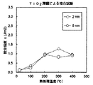
- FIG. 4 is a correlation diagram between film thickness and bonding strength ⁇ at each heating temperature (unheated, 100° C., 200° C., 300° C.), showing bonding test results of a quartz substrate using an ITO thin film as a bonding film.
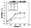
- FIG. 2 is a correlation diagram between film thickness and bonding strength ⁇ at each heating temperature (unheated, 100° C., 200° C., 300° C.), showing bonding test results of a quartz substrate using a WO 3 thin film as a bonding film.
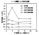
- FIG. 4 is a correlation diagram between waiting time in the atmosphere and bonding strength ⁇ , showing bonding test results of a quartz substrate using an ITO thin film as a bonding film. Explanatory drawing of the "blade method" used for the measurement of bonding strength (free energy of bonding interface) ⁇ (J/m 2 ).
- Bonding of substrates by the chemical bonding method of the present invention is a thin film formed by vacuum deposition such as sputtering or ion plating, and bonding is performed using a thin film of metal or semiconductor with at least an oxidized surface as the bonding film.
- the substrate to be bonded by the chemical bonding method of the present invention may be a substrate having a degree of ultimate vacuum of 1 ⁇ 10 ⁇ 3 to 1 ⁇ 10 ⁇ 8 Pa, preferably 1 ⁇ 10 Pa, for example, by sputtering or ion plating. Any material that can form a bonding film, which will be described in detail later, by vacuum film formation in a high-vacuum atmosphere using a vacuum vessel with a high vacuum of -4 to 1 ⁇ 10 -8 Pa.
- semiconductors such as Si wafers and SiO2 substrates, glasses, ceramics, resins, oxides, etc., which can be vacuum-coated by the above method, are the present invention. It can be used as a base (material to be joined) in the above.
- the two substrates may be not only a combination of the same material, but also a combination of dissimilar materials such as metal and ceramics. According to the above, it is possible to perform suitable bonding.
- the shape of the substrate is not particularly limited.
- substrates of various shapes, from flat plates to various complicated three-dimensional shapes, can be used depending on the application and purpose.
- it is necessary that the portion (bonding surface) where bonding with the other substrate is performed has a smooth surface formed smoothly with a predetermined accuracy.
- a plurality of substrates may be bonded to one substrate.
- the surface roughness of the formed bonding film or oxide thin film is the arithmetic mean height Sa (ISO 4287 ) to form a smooth surface that can be 0.5 nm or less, and when directly superimposed on the above-mentioned bonding film by hydrophilic treatment or surface activation treatment, the smooth surface itself of the substrate is arithmetically averaged It is formed to have a height Sa of 0.5 nm or less.
- the structure of the substrate is not particularly limited, such as single crystal, polycrystal, amorphous, glass state, etc., and various structures can be bonded, but only one of the two substrates is described later.
- a bonding film is formed on the other substrate and the two are bonded without forming a bonding film on the other substrate, there is no chemical bond on the bonding surface of the other substrate on which this bonding film is not formed.
- it is necessary to activate by forming an oxide thin film in advance, by hydrophilizing the surface, or by removing the oxide layer or contaminated layer on the substrate surface by dry etching.
- a bonding film used for bonding must have at least its surface oxidized. As an example, it can be formed as an oxide thin film in which the entire area including the inside is oxidized.
- the material of this bonding film is not limited as long as it forms an oxide that stably exists in a vacuum and in the air. can be used.
- the surface of the bonding film be brought into contact with the entire surface of the film at the atomic level during bonding so that the bonding strength can be improved.
- Such contact at the atomic level reduces the surface roughness (arithmetic mean height Sa) of the bonding film to the same level as the unit cell when the oxide formed at least on the surface of the bonding film is crystalline. It can be realized by setting the size.
- Table 1 below shows the crystal structures and lattice constants of typical oxides.
- the lattice constants of the typical oxides shown below are 0.3 to 0.5 nm, and the surface roughness of the bonding film is defined by the oxides constituting at least the surface of the bonding film.
- the arithmetic mean height (Sa) should be 0.5 nm or less, preferably sufficiently smaller than 0.5 nm, which is the upper limit of the numerical range of the lattice constant, More preferably, it is 0.3 nm or less, which is the lower limit of the numerical range of the lattice constant, so that the bonding interface can be brought into contact at the atomic level through bonding with the OH groups of the adsorbed water molecules.
- the film formation method of the bonding film is not particularly limited as long as it is a vacuum film formation method capable of forming a thin film of metals, semiconductors, or their oxides on the smooth surface of the substrate in a vacuum. , can be formed by various known methods.
- Bonding films formed by such a vacuum deposition method are rapidly cooled (quenched) by high-temperature gas or liquid phase atoms reaching the smooth surface of the substrate during deposition. Due to the presence of many structural defects inside, water molecules are likely to bond with OH groups, and therefore chemical bonding is likely to occur at the bonding interface.
- the bonding film it is possible to perform bonding if it is a metal or semiconductor thin film whose surface is at least oxidized. It is formed as an oxidized oxide thin film.
- the oxide target is sputtered or the oxide solid is evaporated.
- the starting material for film formation itself may be an oxide, such as by vapor deposition, or an oxide produced by reacting an oxide-forming element with oxygen in a vacuum vessel is deposited on the smooth surface of the substrate. It may be formed by forming a film by a method such as a reactive sputtering method that performs deposition.
- oxygen defects and supersaturated oxygen are controlled to increase the defects inside the film, increase the bonding density of water molecules with OH groups, and increase the atomic mobility on the film surface. may be increased, and only a few atomic layers on the surface layer of the bonding film may be formed under such conditions as having many defects.
- An oxide thin film may be formed by post-oxidizing a metal or semiconductor thin film formed by vacuum deposition, such as by oxidizing the thin film, and this may be used as the aforementioned bonding film.
- the above-mentioned bonding film may be obtained by exposing to a space containing oxygen under conditions such that only the surface portion is oxidized.
- Thin films formed by vacuum deposition generally increase in surface roughness as the film thickness increases.
- the film may be formed by using an energy treatment sputtering method (ETS method) in which film formation by sputtering and ion etching are performed simultaneously.
- ETS method energy treatment sputtering method
- the film may be formed by using a bias sputtering method in which sputtering is performed while applying a bias to the substrate.
- the ultimate vacuum of the vacuum vessel is superior to 10 -3 Pa, which is less than 1/100 of the 10 -1 Pa at which the mean free path of the residual gas is about the same as the size of the vacuum vessel. It is necessary to be
- the pressure is higher than 10 -4 Pa, which corresponds to 1 Langmuir.
- the lattice constant (0.3 ⁇ 0.5 nm), the lower limit of which is 0.3 nm, preferably 0.5 nm.
- a thick thin film may be required from the viewpoint of breakdown voltage.
- a thin film having a certain thickness or more may be required from the viewpoint of the wavelength.
- the ETS method and the bias sputtering method described above it is possible to form a bonding film with a small surface roughness while increasing the thickness. requires a very long film-forming time, making it difficult to form industrially, the upper limit of the thickness of the bonding film is 5 ⁇ m, preferably 1 ⁇ m.
- the film thickness of the bonding film is preferably in the range of 0.3 nm to 5 ⁇ m, more preferably 0.5 nm to 1 ⁇ m.
- Such hydrophilization may be carried out by removing the substrate on which the bonding film is formed by vacuum film formation from the vacuum chamber into the atmosphere. Hydrophilization takes place.
- the hydrophilization of the bonding film may be performed in the vacuum chamber by introducing moisture or air containing moisture into the vacuum chamber in which the bonding film was formed.
- a metal or semiconductor thin film (unoxidized) is formed by vacuum film formation, and after the film is formed, the metal or semiconductor thin film is exposed to a space containing oxygen to oxidize it afterwards.
- oxidation and hydrophilization may be performed at the same time by taking out the substrate on which the thin film of metal or semiconductor formed by vacuum film formation is formed into the atmosphere.
- the bonding film when the bonding film is made hydrophilic by taking it out into the air, the surface of the bonding film becomes hydrophobic as the surface contamination of organic molecules progresses with the passage of time and becomes chemically stabilized. , Bonding must be performed in a hydrophilized state before such hydrophobicity.
- the bonding strength hardly changed within 2 hours after being taken out into the atmosphere. After 2 hours, the bonding strength gradually decreases, but even after 24 hours, the bonding strength is about 70% of the bonding strength immediately after removal without heating, and about 90% after heating at 300°C. Furthermore, even after 165 hours (1 week), the value of about 40% was maintained without heating and about 70% after heating at 300°C.
- both the hydrophilization of the bonding film and the superposition of the substrates may be performed in the atmosphere.
- the substrates having the bonding films hydrophilized may be taken out of the vacuum vessel and stacked in an inert gas atmosphere to be bonded.
- an inert gas is sealed together with the electronic device in the package to oxidize the electronic device. It may be possible to protect against deterioration due to the like.
- a bonding film is formed only on the smooth surface of one substrate to be bonded, and an oxide thin film is formed on the smooth surface of the other substrate by a known method, or the surface can be hydrophilized or activated by a known method to make it easy to chemically bond, and the smooth surface of one of the substrates having the bonding film formed thereon can be superimposed thereon.
- the oxide thin film formed on the other substrate need not be of the same material as the bonding film formed on the smooth surface of the other substrate, and may be of a different material.
- the smooth surface of the other substrate is activated by dry etching or the like to remove the oxide layer or contaminant layer formed on the smooth surface of the other substrate in the same vacuum as the bonding film is formed. It may be carried out by removing.
- the material of the other substrate may be a metal, a semiconductor such as Si, or an oxide of these. It may be present, and its material is not limited.
- a bonding film formed of an oxide thin film can be used to provide electrical insulation between the substrates to be bonded and optical isolation between the substrates. It can also be used for adjusting properties.
- the substrates bonded as described above may be further heated by a known method after bonding to improve the bonding strength ⁇ .
- the heating temperature is not particularly limited, but when a substrate on which an electronic device or the like is mounted is to be bonded, the temperature is preferably 400°C or less in order to prevent damage to the electronic device or the like. By doing so, it is possible to greatly improve the bonding strength compared to the case of no heating.
- the bonding strength can be improved in any case, whether the heating temperature is raised stepwise to the target temperature or the heating temperature is raised to the target temperature at once.
- Film formation was performed by RF magnetron sputtering or bias sputtering under the conditions shown in Table 2 below.
- test results that are not specifically described are the results of bonding using a bonding film formed by the RF magnetron sputtering method.
- Both bonding films formed by any of the methods were vented with nitrogen gas in a load lock chamber of a sputtering device, then taken out into the air with a humidity of 50% (room temperature 20° C.) to be hydrophilized, and two substrates were separated. were overlapped and bonded without applying pressure so that the bonding films were in contact with each other.
- the free energy of the bonding interface was measured by the blade method for each of the unheated one and the one heated at each temperature of 100°C, 200°C, and 300°C (further 400°C in some test examples) for 5 minutes. ⁇ (J/m 2 ) was measured as bonding strength.
- the blade method is based on the peeling length L from the tip of the blade when the blade is inserted into the bonding interface of the two substrates, based on the bonding strength (surface free energy of the bonding interface) ⁇
- the bonding strength ⁇ is expressed by the following equation [MP Maszara. G. Goetz. A. Cavigila and J. B. McKitterick: J. Appl. Phys. 64 (1988) 4943].
- ⁇ 3 / 8 ⁇ Et3y2 /L4 where E is the Young's modulus of the wafer, t is the thickness of the wafer, and y is half the thickness of the blade.
- the arithmetic mean height Sa of the surface of the Y 2 O 3 thin film was about 0.14 nm or less, which is approximately the same as the arithmetic mean height Sa of the quartz substrate surface.
- the bonding strength improved as the heating temperature increased, and was 0.82 to 0 by heating at 300° C. up to .90 J/m 2 .
- the bonding by the chemical bonding method of the present invention is suitable for bonding parts that require transparency at the bonding part, and uniform bonding conditions. It was able to withstand use for bonding (insulating parts) of electronic parts, etc., which require good properties.
- the Y 2 O 3 thin film contained microcrystals inside, and the heat treatment caused atomic rearrangements where the junction interface had disappeared.
- the bonding strength ⁇ is 0.14 to 0.17 J/m 2 without heating. It showed a tendency to increase as the temperature increased, and when the heating temperature was increased to 300°C, the bonding strength increased to 0.37 to 0.57 J/m 2 .
- the unheated bond strength ⁇ was 0.10 J/m 2 , a significant drop compared to the film thickness of 2 to 10 nm.
- the bonding strength .gamma. is low, it has been confirmed that the substrates can be bonded even when a ZrO.sub.2 thin film having a thickness of 20 nm is used as the bonding film.
- the bonding by the chemical bonding method of the present invention is suitable for bonding parts that require transparency at the bonding part, and uniform bonding conditions. It was able to withstand use for bonding (insulating parts) of electronic parts, etc., which require good properties.
- the bonding strength ⁇ is 0.1 J/m 2 when unheated, but reaches 1 J/m 2 when heated to 200°C. , the bond strength ⁇ peaked out without any significant change.
- the arithmetic mean height Sa of the ITO thin film surface was about 0.15 nm or less, and both were about the same as the arithmetic mean height Sa of the quartz substrate surface.
- the bonding strength ⁇ was 0.2 J/m 2 before heating, but it was confirmed that the bonding strength ⁇ increased with increasing heating temperature for all film thicknesses.
- the bond strength ⁇ reached 1.8 J/m 2 with a film thickness of 5 nm, and a relatively high bond strength of 0.8 to 1.2 J/m 2 was obtained with other film thicknesses. was taken.
- FIG. 4 shows the bonding strength of a sample (Example) bonded in the atmosphere using an ITO thin film with a thickness of 5 nm by the method of the present invention, and the quartz substrate on which an ITO thin film with a thickness of 5 nm was formed. Comparison results of a sample (comparative example) bonded in a vacuum without being removed from the vacuum container are shown.
- the bonding strength ⁇ of the example of 1.7 J/m 2 obtained by heating at 300° C. after bonding in the air is The bonding strength ⁇ of the comparative example obtained when the sample bonded in vacuum is heated at 300°C is about the same, and depending on the conditions, even bonding in the atmosphere can achieve the same level of firm bonding as bonding in a vacuum. I know you can get it.
- the bonding strength ⁇ for film thicknesses of 1 nm and 2 nm was 0.17 J/m 2 before heating, and increased as the heating temperature increased.
- the intensity ⁇ was 0.87 J/m 2 (film thickness 2 nm).
- the arithmetic mean height Sa of the surface increases sharply as the film thickness increases. is getting smaller.
- bonding can be performed in any example using a SiO 2 thin film of any film thickness as a bonding film.
- the bonding method of the present invention in which the substrate on which the SiO2 thin film is formed is taken out into the air and bonded, is higher than in the case of bonding in a vacuum without removing the substrate on which the SiO2 thin film is formed from the vacuum vessel. It has been confirmed that the bonding strength ⁇ is exhibited.
- FIG. 6 shows the results of measuring the bonding strength.
- the arithmetic mean height Sa of the surface of the WO 3 thin film was constant at about 0.12 nm and maintained at the same level as the arithmetic mean height Sa of the quartz substrate surface.
- the bonding strength ⁇ is about 0.2 J/m 2 before heating for any film thickness, and is about 0.9 J/m 2 at maximum after heating at 300°C (film thickness 5, 10 nm). Thickness dependence is relatively small.
- the plot indicated as "Si substrate (5 nm/300°C)" in Fig. 6 shows the bonding strength of a sample in which a Si substrate on which a WO3 film with a thickness of 5 nm was formed was bonded in the air and then heated at once to 300°C. ⁇ is displayed, and in this example, the bonding strength ⁇ increased to 1.36 J/m 2 .
- Table 6 shows only the measurement results of the film thicknesses of 2 nm and 5 nm, which are substantially common to each other in that the surface arithmetic mean height Sa is 0.16 nm or less, among the results of the bonding tests using the bonding films described above. (However, only the SiO 2 film with a thickness of 5 nm has a somewhat large arithmetic mean height Sa of 0.22 nm).
- the bonding strength ⁇ after heat treatment at 300°C indicates the bonding strength ⁇ when heated in steps of 100°C at a time of heating to 300°C. ).
- the bonding strength ⁇ is increased by heating after bonding in any bonding film, and it has been confirmed that heating after bonding is effective in improving the bonding strength ⁇ .
- the bonding strength ⁇ was further improved by changing the heating conditions so as to heat the other bonding films at once to the target temperature. It is assumed that
- the heating temperature was further increased to 400°C and the change in the bonding strength ⁇ was measured, but no further improvement in the bonding strength ⁇ was observed.
- heating is performed after bonding, it has been confirmed that heating at 400° C. or less, for example, about 300° C., which hardly damages electronic devices, is effective in improving the bonding strength ⁇ .
- the measurement results after heat treatment at 300°C are obtained by measuring the bonding strength ⁇ when the heating temperature is increased stepwise by 100°C after bonding and reaches 300°C.
- the constituent element of quartz is SiO2 , which is common to the SiO2 thin film formed as the bonding film. It can be seen that bonding with a SiO 2 thin film formed by a film intervening as a bonding film yields a significantly higher bonding strength ⁇ both before heating and after heating at 300°C.
- bonding can be performed even by increasing the film thickness as long as the surface roughness of the bonding film used for bonding can be maintained within a predetermined range.
- the arithmetic mean height Sa of the surface of the ITO thin film with a film thickness of 5 nm was about 0.15 nm or less, which was about the same as the arithmetic mean height Sa of the quartz substrate surface.
- the bonding strength ⁇ showed almost no decrease within 2 hours of waiting time.
- the bonding strength ⁇ gradually decreases, but even after 24 hours, the bonding strength ⁇ is 74% (unheated) to 91% (after heating at 300°C) when bonding immediately after removal to the atmosphere. It was confirmed that the bonding strength ⁇ of
- the bonding was performed quickly (within 5 minutes) after the substrate was removed from the vacuum chamber.
- the bonding strength ⁇ of the quartz substrate after bonding was measured in the unheated state, when heated at 200°C, and when heated at 300°C. Table 10 shows the measurement results.
- the heating of the substrate was performed by increasing the heating temperature stepwise by 100°C using a hot plate.
- both the 0.3 nm thick Ti thin film and the 0.5 nm thick Ti thin film were transparent, confirming that they were oxidized when taken out into the atmosphere.
- the bond strength ⁇ in the unheated state showed a larger value in the case where the vacuum chamber was vented with nitrogen (N 2 ) gas, but it was confirmed that bonding could be performed in any of the samples.
- the bonding strength ⁇ after heating increases as the film thickness increases, and the bonding strength ⁇ after heating at 300°C is as high as about 1 J/m 2 for the film thicknesses of 0.3 nm and 0.5 nm. In the case of 1.0 nm, the blade could not be inserted, and the bonding strength ⁇ was so high that the quartz substrate was broken if it was inserted forcibly.
- the bonding was performed within 5 minutes after being taken out into the atmosphere.
- the bonding strength ⁇ after bonding was measured in an unheated state, when heated to 200 ° C., and when heated to 300 ° C., and the substrate was heated in steps of 100 ° C. using a hot plate. This was done by increasing the temperature.
- both the Zr thin films with a thickness of 0.3 nm and a thickness of 0.5 nm were transparent, confirming that they were oxidized when taken out into the air.
- the bonding strength ⁇ in the unheated state was relatively small, about 0.02 to 0.03 J/m 2 , but it was confirmed that bonding could be performed.
- the bonding strength ⁇ of bonding an ITO film and a surface-oxidized Ti film was 0.35 (J/m 2 ) even without heating, which is greater than that of bonding ITO thin films. .
- the bonding strength ⁇ after heating at 300° C. is 1.23 J/m 2 , which is smaller than that obtained when ITO thin films are bonded together, but a large bonding strength exceeding 1 J/m 2 is obtained.
- Table 13 shows the results of bonding with a 5 nm thick ITO thin film formed on one substrate and the other substrate without a thin film formed. rice field. It shows the result of joining the ITO thin film within 5 minutes after taking it out of the vacuum vessel. The table also shows the results of bonding ITO thin films with a thickness of 5 nm to each other and the results of bonding two quartz substrates in the atmosphere (optical contact) without forming a thin film. These are the same as the results shown in Experimental Example 1.
- the bonding strength ⁇ of a 5 nm-thick ITO thin film formed on one of the substrates was 0.26 (J/m 2 ) before heating and 0.41 (J/m 2 ) after heating at 300°C. have been obtained.
- bonding with an ITO thin film interposed on one of the substrates as a bonding film is significantly better in both unheated and after heating at 300°C.
- a large bonding strength ⁇ is obtained.
- the bonding strength ⁇ in the case where an ITO thin film with a thickness of 5 nm is formed on one substrate and bonded is slightly larger in the unheated state than in the case where the ITO thin film is formed on both substrates. have been obtained. This is because the surface roughness of the quartz substrate on which the ITO thin film is not formed is slightly smaller than that of the ITO film. This is probably because hydrogen bonding is likely to occur.
- the bonding strength ⁇ after heating at 300° C. is greater when the ITO films are formed on both sides. This is probably because the thin film surface of the ITO film has a large number of defects, and therefore, when the ITO film is formed on both sides, it is easier for the atoms to bond at the contact interface by performing the heat treatment.
Landscapes
- Chemical & Material Sciences (AREA)
- Engineering & Computer Science (AREA)
- Mechanical Engineering (AREA)
- Chemical Kinetics & Catalysis (AREA)
- Materials Engineering (AREA)
- Metallurgy (AREA)
- Organic Chemistry (AREA)
- Pressure Welding/Diffusion-Bonding (AREA)
- Manufacturing & Machinery (AREA)
Priority Applications (8)
| Application Number | Priority Date | Filing Date | Title |
|---|---|---|---|
| PCT/JP2021/004913 WO2022172349A1 (ja) | 2021-02-10 | 2021-02-10 | 化学結合法及びパッケージ型電子部品 |
| KR1020237030331A KR20230143167A (ko) | 2021-02-10 | 2022-02-07 | 화학 결합법 및 패키지형 전자 부품, 그리고 전자 디바이스의 하이브리드 접합법 |
| CN202280003691.3A CN115443203B (zh) | 2021-02-10 | 2022-02-07 | 化学结合法和封装型电子部件、以及电子器件的混合接合法 |
| PCT/JP2022/004758 WO2022172902A1 (ja) | 2021-02-10 | 2022-02-07 | 化学結合法及びパッケージ型電子部品,並びに電子デバイスのハイブリッド接合法 |
| JP2022550117A JP7165342B1 (ja) | 2021-02-10 | 2022-02-07 | 化学結合法及びパッケージ型電子部品,並びに電子デバイスのハイブリッド接合法 |
| EP22752725.6A EP4292747A4 (en) | 2021-02-10 | 2022-02-07 | Chemical bonding method, encapsulation-type electronic component, and hybrid bonding method for electronic device |
| TW111104686A TWI884358B (zh) | 2021-02-10 | 2022-02-09 | 化學鍵結法、封裝型電子元件及電子裝置之混合接合法 |
| US17/962,061 US11916038B2 (en) | 2021-02-10 | 2022-10-07 | Chemical bonding method, package-type electronic component, and hybrid bonding method for electronic device |
Applications Claiming Priority (1)
| Application Number | Priority Date | Filing Date | Title |
|---|---|---|---|
| PCT/JP2021/004913 WO2022172349A1 (ja) | 2021-02-10 | 2021-02-10 | 化学結合法及びパッケージ型電子部品 |
Publications (1)
| Publication Number | Publication Date |
|---|---|
| WO2022172349A1 true WO2022172349A1 (ja) | 2022-08-18 |
Family
ID=82837841
Family Applications (2)
| Application Number | Title | Priority Date | Filing Date |
|---|---|---|---|
| PCT/JP2021/004913 Ceased WO2022172349A1 (ja) | 2021-02-10 | 2021-02-10 | 化学結合法及びパッケージ型電子部品 |
| PCT/JP2022/004758 Ceased WO2022172902A1 (ja) | 2021-02-10 | 2022-02-07 | 化学結合法及びパッケージ型電子部品,並びに電子デバイスのハイブリッド接合法 |
Family Applications After (1)
| Application Number | Title | Priority Date | Filing Date |
|---|---|---|---|
| PCT/JP2022/004758 Ceased WO2022172902A1 (ja) | 2021-02-10 | 2022-02-07 | 化学結合法及びパッケージ型電子部品,並びに電子デバイスのハイブリッド接合法 |
Country Status (7)
| Country | Link |
|---|---|
| US (1) | US11916038B2 (https=) |
| EP (1) | EP4292747A4 (https=) |
| JP (1) | JP7165342B1 (https=) |
| KR (1) | KR20230143167A (https=) |
| CN (1) | CN115443203B (https=) |
| TW (1) | TWI884358B (https=) |
| WO (2) | WO2022172349A1 (https=) |
Cited By (1)
| Publication number | Priority date | Publication date | Assignee | Title |
|---|---|---|---|---|
| WO2025169311A1 (ja) * | 2024-02-06 | 2025-08-14 | 国立大学法人東北大学 | マイクロ流路デバイス及びマイクロ流路デバイスの製造方法 |
Families Citing this family (2)
| Publication number | Priority date | Publication date | Assignee | Title |
|---|---|---|---|---|
| US12532780B2 (en) * | 2022-08-22 | 2026-01-20 | Micron Technology, Inc. | Hybrid bonding for semiconductor device assemblies |
| EP4350329A1 (en) * | 2022-10-06 | 2024-04-10 | The Procter & Gamble Company | Methods for quantification of solvent-substrate interactions |
Citations (4)
| Publication number | Priority date | Publication date | Assignee | Title |
|---|---|---|---|---|
| JP2012023326A (ja) * | 2009-09-04 | 2012-02-02 | Sumitomo Chemical Co Ltd | 半導体基板、電界効果トランジスタ、集積回路、及び半導体基板の製造方法 |
| JP2014022699A (ja) * | 2012-07-24 | 2014-02-03 | Nippon Telegr & Teleph Corp <Ntt> | パッケージおよびその製造方法 |
| JP2014138136A (ja) * | 2013-01-18 | 2014-07-28 | Tokyo Electron Ltd | 接合方法、プログラム、コンピュータ記憶媒体及び接合システム |
| JP2014221492A (ja) * | 2014-06-19 | 2014-11-27 | 株式会社ムサシノエンジニアリング | 原子拡散接合方法 |
Family Cites Families (40)
| Publication number | Priority date | Publication date | Assignee | Title |
|---|---|---|---|---|
| JPS541661U (https=) | 1977-06-06 | 1979-01-08 | ||
| JPS5569964U (https=) | 1978-11-09 | 1980-05-14 | ||
| US5372851A (en) * | 1991-12-16 | 1994-12-13 | Matsushita Electric Industrial Co., Ltd. | Method of manufacturing a chemically adsorbed film |
| JP3704258B2 (ja) * | 1998-09-10 | 2005-10-12 | 松下電器産業株式会社 | 薄膜形成方法 |
| TWI330269B (en) * | 2002-12-27 | 2010-09-11 | Semiconductor Energy Lab | Separating method |
| WO2005055293A1 (ja) * | 2003-12-02 | 2005-06-16 | Bondtech Inc. | 接合方法及びこの方法により作成されるデバイス並びに表面活性化装置及びこの装置を備えた接合装置 |
| JP2007115825A (ja) * | 2005-10-19 | 2007-05-10 | Bondtech Inc | 表面活性化方法および表面活性化装置 |
| US8039401B2 (en) * | 2007-12-14 | 2011-10-18 | Fairchild Semiconductor Corporation | Structure and method for forming hybrid substrate |
| JP2009289953A (ja) * | 2008-05-29 | 2009-12-10 | Hitachi Ulsi Systems Co Ltd | ウェハレベルパッケージ、ウェハレベルパッケージの製造方法及びmemsデバイスの製造方法 |
| JP5401661B2 (ja) | 2008-08-22 | 2014-01-29 | 株式会社ムサシノエンジニアリング | 原子拡散接合方法及び前記方法により接合された構造体 |
| JP4843012B2 (ja) * | 2008-11-17 | 2011-12-21 | 日本電波工業株式会社 | 圧電デバイスとその製造方法 |
| JP5569964B2 (ja) | 2010-05-07 | 2014-08-13 | 株式会社ムサシノエンジニアリング | 原子拡散接合方法 |
| US8557679B2 (en) * | 2010-06-30 | 2013-10-15 | Corning Incorporated | Oxygen plasma conversion process for preparing a surface for bonding |
| JP2012065305A (ja) * | 2010-08-20 | 2012-03-29 | Nippon Dempa Kogyo Co Ltd | 圧電デバイスの製造方法及び圧電デバイス |
| JP5783252B2 (ja) | 2011-07-29 | 2015-09-24 | 株式会社村田製作所 | 弾性波デバイスの製造方法 |
| US9620560B2 (en) * | 2011-08-26 | 2017-04-11 | Joled Inc. | EL display device and method for manufacturing same |
| US8809123B2 (en) * | 2012-06-05 | 2014-08-19 | Taiwan Semiconductor Manufacturing Company, Ltd. | Three dimensional integrated circuit structures and hybrid bonding methods for semiconductor wafers |
| WO2014046052A1 (ja) * | 2012-09-23 | 2014-03-27 | 国立大学法人東北大学 | チップ支持基板、チップ支持方法、三次元集積回路、アセンブリ装置及び三次元集積回路の製造方法 |
| FR3025051A1 (fr) * | 2014-08-22 | 2016-02-26 | Commissariat Energie Atomique | Procede de realisation d'un circuit integre par collage direct de substrats comprenant en surface des portions de cuivre et de materiau dielectrique |
| FR3027250B1 (fr) * | 2014-10-17 | 2019-05-03 | Commissariat A L'energie Atomique Et Aux Energies Alternatives | Procede de collage direct via des couches metalliques peu rugueuses |
| US9536853B2 (en) * | 2014-11-18 | 2017-01-03 | International Business Machines Corporation | Semiconductor device including built-in crack-arresting film structure |
| US9953941B2 (en) * | 2015-08-25 | 2018-04-24 | Invensas Bonding Technologies, Inc. | Conductive barrier direct hybrid bonding |
| CN105197881A (zh) * | 2015-08-28 | 2015-12-30 | 中国科学院半导体研究所 | 一种利用金属材料扩散互溶实现硅-硅键合的方法 |
| JP6294417B2 (ja) * | 2016-09-01 | 2018-03-14 | 日機装株式会社 | 光半導体装置および光半導体装置の製造方法 |
| US9892920B1 (en) * | 2017-01-05 | 2018-02-13 | Lam Research Corporation | Low stress bonding of silicon or germanium parts |
| CN110651359A (zh) * | 2017-05-25 | 2020-01-03 | 株式会社新川 | 结构体的制造方法及结构体 |
| JP2019117311A (ja) * | 2017-12-27 | 2019-07-18 | マルミ光機株式会社 | Ndフィルターおよびその製造方法 |
| JP7018126B2 (ja) * | 2018-04-20 | 2022-02-09 | 富士フイルム株式会社 | 導熱層、感光層、感光性組成物、導熱層の製造方法、並びに、積層体および半導体デバイス |
| US10937743B2 (en) * | 2018-04-30 | 2021-03-02 | Taiwan Semiconductor Manufacturing Company, Ltd. | Mixing organic materials into hybrid packages |
| CN116364659A (zh) * | 2018-06-29 | 2023-06-30 | 长江存储科技有限责任公司 | 半导体结构及其形成方法 |
| JP6986105B2 (ja) | 2018-07-05 | 2021-12-22 | エーファウ・グループ・エー・タルナー・ゲーエムベーハー | ウエハの永久接合方法 |
| EP3670998B1 (de) | 2018-12-18 | 2022-11-16 | Nexans | Kupplung für fluidführende leitungen |
| JP7199743B2 (ja) * | 2018-12-28 | 2023-01-06 | 国立研究開発法人産業技術総合研究所 | グラファイト薄膜/シリコン基板積層体、及びその製造方法、高排熱型電子デバイス用基板 |
| KR20200098031A (ko) | 2019-02-11 | 2020-08-20 | 주식회사 엘지화학 | 에어 필터 및 그 제조 방법 |
| US11557692B2 (en) * | 2019-06-11 | 2023-01-17 | Meta Platforms Technologies, Llc | Selectively bonding light-emitting devices via a pulsed laser |
| FR3098985B1 (fr) * | 2019-07-15 | 2022-04-08 | Soitec Silicon On Insulator | Procédé de collage hydrophile de substrats |
| JP7131778B2 (ja) | 2019-09-05 | 2022-09-06 | 国立大学法人東北大学 | 化学結合法及び接合構造体 |
| EP4026644A4 (en) * | 2019-09-05 | 2023-09-27 | Tohoku University | CHEMICAL BONDING METHOD AND BONDED STRUCTURE |
| WO2021131080A1 (ja) * | 2019-12-27 | 2021-07-01 | ボンドテック株式会社 | 接合方法、被接合物および接合装置 |
| JP2021190932A (ja) * | 2020-06-03 | 2021-12-13 | セイコーエプソン株式会社 | 振動子及び発振器 |
-
2021
- 2021-02-10 WO PCT/JP2021/004913 patent/WO2022172349A1/ja not_active Ceased
-
2022
- 2022-02-07 CN CN202280003691.3A patent/CN115443203B/zh active Active
- 2022-02-07 EP EP22752725.6A patent/EP4292747A4/en active Pending
- 2022-02-07 JP JP2022550117A patent/JP7165342B1/ja active Active
- 2022-02-07 KR KR1020237030331A patent/KR20230143167A/ko active Pending
- 2022-02-07 WO PCT/JP2022/004758 patent/WO2022172902A1/ja not_active Ceased
- 2022-02-09 TW TW111104686A patent/TWI884358B/zh active
- 2022-10-07 US US17/962,061 patent/US11916038B2/en active Active
Patent Citations (4)
| Publication number | Priority date | Publication date | Assignee | Title |
|---|---|---|---|---|
| JP2012023326A (ja) * | 2009-09-04 | 2012-02-02 | Sumitomo Chemical Co Ltd | 半導体基板、電界効果トランジスタ、集積回路、及び半導体基板の製造方法 |
| JP2014022699A (ja) * | 2012-07-24 | 2014-02-03 | Nippon Telegr & Teleph Corp <Ntt> | パッケージおよびその製造方法 |
| JP2014138136A (ja) * | 2013-01-18 | 2014-07-28 | Tokyo Electron Ltd | 接合方法、プログラム、コンピュータ記憶媒体及び接合システム |
| JP2014221492A (ja) * | 2014-06-19 | 2014-11-27 | 株式会社ムサシノエンジニアリング | 原子拡散接合方法 |
Cited By (1)
| Publication number | Priority date | Publication date | Assignee | Title |
|---|---|---|---|---|
| WO2025169311A1 (ja) * | 2024-02-06 | 2025-08-14 | 国立大学法人東北大学 | マイクロ流路デバイス及びマイクロ流路デバイスの製造方法 |
Also Published As
| Publication number | Publication date |
|---|---|
| US11916038B2 (en) | 2024-02-27 |
| WO2022172902A1 (ja) | 2022-08-18 |
| EP4292747A4 (en) | 2025-03-19 |
| EP4292747A1 (en) | 2023-12-20 |
| KR20230143167A (ko) | 2023-10-11 |
| CN115443203A (zh) | 2022-12-06 |
| CN115443203B (zh) | 2024-07-16 |
| JP7165342B1 (ja) | 2022-11-04 |
| JPWO2022172902A1 (https=) | 2022-08-18 |
| TWI884358B (zh) | 2025-05-21 |
| TW202245164A (zh) | 2022-11-16 |
| US20230051810A1 (en) | 2023-02-16 |
Similar Documents
| Publication | Publication Date | Title |
|---|---|---|
| JP7165342B1 (ja) | 化学結合法及びパッケージ型電子部品,並びに電子デバイスのハイブリッド接合法 | |
| KR101453135B1 (ko) | 직접 접합 방법에서의 질소-플라즈마 표면 처리 | |
| EP3306644B1 (en) | Method for producing composite wafer provided with oxide single-crystal thin film | |
| JP2021528870A (ja) | 共有接合半導体インターフェース | |
| CN102422396B (zh) | 基板处理方法和结晶性碳化硅(sic)基板的制造方法 | |
| TWI826971B (zh) | 用於接觸表面之接合之方法 | |
| KR102420245B1 (ko) | 기판 본딩 장치 및 방법 | |
| CN104737273B (zh) | 通过分子粘附来键合的方法 | |
| TW201250784A (en) | Method for permanent bonding of wafers | |
| WO2013088226A1 (en) | Process for stabilizing a bonding interface, located within a structure which comprises an oxide layer and structure obtained | |
| KR101952492B1 (ko) | 웨이퍼 본딩 방법 및 그 제조 방법에 의해 제조된 삼차원 구조의 반도체 반도체 소자 | |
| JP7131778B2 (ja) | 化学結合法及び接合構造体 | |
| US20260100716A1 (en) | Antirelaxation Coatings for Vapor Cells | |
| EP0804801B1 (fr) | Boite de stockage d'un objet destine a etre protege d'une contamination physico-chimique | |
| JP7390619B2 (ja) | 原子拡散接合法及び接合構造体 | |
| EP4026644A1 (en) | Chemical bonding method and joined structure | |
| KR20240169017A (ko) | 복합 기판 형성 방법 | |
| JP7825844B1 (ja) | 原子拡散接合法 | |
| WO2025142238A1 (ja) | 複合基板、複合基板の製造方法 | |
| CN121729081A (zh) | 玻璃晶圆与玻璃基板的低温键合工艺 | |
| JPH0484431A (ja) | ウェーハの保管方法 | |
| JPS6179230A (ja) | 半導体基板の処理方法 | |
| WO2019060050A1 (en) | REDUCTION OF NATIVE OR NON-CONTROLLED OXIDE BY CYCLIC PLASMA TREATMENT PROCESS AND RADICAL H * | |
| JPH0279421A (ja) | Si上への3−V族化合物半導体エピ成長の前処理方法 |
Legal Events
| Date | Code | Title | Description |
|---|---|---|---|
| 121 | Ep: the epo has been informed by wipo that ep was designated in this application |
Ref document number: 21925603 Country of ref document: EP Kind code of ref document: A1 |
|
| NENP | Non-entry into the national phase |
Ref country code: DE |
|
| 122 | Ep: pct application non-entry in european phase |
Ref document number: 21925603 Country of ref document: EP Kind code of ref document: A1 |
|
| NENP | Non-entry into the national phase |
Ref country code: JP |