WO2022124205A1 - 光スイッチ素子、光スイッチ装置、光通信システム及び光コンピュータ - Google Patents
光スイッチ素子、光スイッチ装置、光通信システム及び光コンピュータ Download PDFInfo
- Publication number
- WO2022124205A1 WO2022124205A1 PCT/JP2021/044368 JP2021044368W WO2022124205A1 WO 2022124205 A1 WO2022124205 A1 WO 2022124205A1 JP 2021044368 W JP2021044368 W JP 2021044368W WO 2022124205 A1 WO2022124205 A1 WO 2022124205A1
- Authority
- WO
- WIPO (PCT)
- Prior art keywords
- optical switch
- optical
- switch element
- light
- transition metal
- Prior art date
- Legal status (The legal status is an assumption and is not a legal conclusion. Google has not performed a legal analysis and makes no representation as to the accuracy of the status listed.)
- Ceased
Links
Images







Classifications
-
- G—PHYSICS
- G02—OPTICS
- G02F—OPTICAL DEVICES OR ARRANGEMENTS FOR THE CONTROL OF LIGHT BY MODIFICATION OF THE OPTICAL PROPERTIES OF THE MEDIA OF THE ELEMENTS INVOLVED THEREIN; NON-LINEAR OPTICS; FREQUENCY-CHANGING OF LIGHT; OPTICAL LOGIC ELEMENTS; OPTICAL ANALOGUE/DIGITAL CONVERTERS
- G02F1/00—Devices or arrangements for the control of the intensity, colour, phase, polarisation or direction of light arriving from an independent light source, e.g. switching, gating or modulating; Non-linear optics
- G02F1/01—Devices or arrangements for the control of the intensity, colour, phase, polarisation or direction of light arriving from an independent light source, e.g. switching, gating or modulating; Non-linear optics for the control of the intensity, phase, polarisation or colour
- G02F1/09—Devices or arrangements for the control of the intensity, colour, phase, polarisation or direction of light arriving from an independent light source, e.g. switching, gating or modulating; Non-linear optics for the control of the intensity, phase, polarisation or colour based on magneto-optical elements, e.g. exhibiting Faraday effect
-
- H—ELECTRICITY
- H04—ELECTRIC COMMUNICATION TECHNIQUE
- H04Q—SELECTING
- H04Q11/00—Selecting arrangements for multiplex systems
- H04Q11/0001—Selecting arrangements for multiplex systems using optical switching
- H04Q11/0005—Switch and router aspects
-
- H—ELECTRICITY
- H04—ELECTRIC COMMUNICATION TECHNIQUE
- H04Q—SELECTING
- H04Q11/00—Selecting arrangements for multiplex systems
- H04Q11/0001—Selecting arrangements for multiplex systems using optical switching
- H04Q11/0005—Switch and router aspects
- H04Q2011/0007—Construction
Definitions
- the present invention relates to an optical switch element, an optical switch device, an optical communication system, and an optical computer.
- the magneto-optical switch is an example of an element using spin.
- the photomagnetic switch is a switch that utilizes the property that the turning property changes when a circularly polarized pulse is applied to a substance having magnetic order such as an antiferromagnetic material or a weakly ferromagnetic material.
- Patent Document 1 describes a magneto-optical switch that utilizes a magneto-optical effect.
- the magneto-optical switch described in Patent Document 1 requires that the spins of adjacent sub-lattices have magnetic order. This is because the magneto-optical switch described in Patent Document 1 utilizes the reverse Faraday effect.
- the Faraday effect has been considered to be a phenomenon limited to magnetic materials having long-range magnetic order (for example, antiferromagnetic materials and weak ferromagnetic materials).
- the orbital motion of electrons excited by circular polarization reveals the magnetization in the material by spin-orbit interaction.
- the photomagnetic switch described in Patent Document 1 operates only at a Néel temperature TN or a Curie temperature T c or less in which an antiferromagnetic material, a weak ferromagnetic material, or the like has a long-range magnetic order.
- the Néel temperature TN and the Curie temperature T c are extremely low temperatures (for example, 7 K or less).
- the magneto-optical switch described in Patent Document 1 uses a substance having a relatively high Curie temperature, but the temperature range in which it can be used is still limited.
- the present invention has been made in view of the above problems, and an object of the present invention is to provide an optical switch element, an optical switch device, an optical communication system, and an optical computer that can operate even in a temperature range higher than the Néel temperature.
- the present invention provides the following means for solving the above problems.
- the optical switch element according to the first aspect is a substance having a plurality of transition metal elements having electrons in the d orbit and a plurality of anions arranged around each of the plurality of transition metal elements.
- the state in which the plurality of transition metal elements are arranged in a grid pattern, the t 2g orbitals in which the d orbitals of the plurality of transition metal elements are split are connected in a ring shape, and the substance does not have long-range magnetic order. Then, when the control light is irradiated, the signal light is polarized and rotated.
- the arrangement of the plurality of transition metal elements may be any of a honeycomb lattice shape, a triangular lattice shape, and a kagome lattice shape.
- the substance may be ⁇ -RuCl 3 .
- the wavelength of the control light may be 1 ⁇ m or more.
- the optical switch device includes the optical switch element according to the above aspect, a light source that irradiates the optical switch element with the signal light, and a control element that irradiates the optical switch element with the control light. And a polarizing plate that polarizes the light transmitted or reflected through the optical switch element.
- the optical communication system according to the third aspect includes the optical switch device according to the above aspect.
- the optical computer according to the fourth aspect includes the optical switch device according to the above aspect.
- the optical switch element, the optical switch device, the optical communication system, and the optical computer according to the above aspect can operate even in a temperature range higher than the Neel temperature.
- the time change of the polarization rotation by the circular polarization excitation in the optical switch element of Example 1 is shown.
- the time change of the polarization rotation by the circular polarization excitation in the optical switch element of Example 2 is shown. It is the measurement result of Example 3 and shows the temperature dependence of the maximum value of the rotation angle of the polarization rotation by the circular polarization excitation.
- the time change of the plane component of the magnetization generated in ⁇ -RuCl 3 by the circular polarization excitation obtained by the theoretical calculation of Example 4 is shown.
- the measurement result of Example 5 is shown. It shows the time change of the rotation angle in the polarization direction when the photon energy of the control light is changed to 1.55 eV (wavelength 800 nm).
- the traveling direction of the signal light L1 emitted from the light source 20 is the z direction
- one direction in the plane orthogonal to the z direction is the x direction
- the z direction and the direction orthogonal to the x direction are the y direction.
- the growth direction of the crystal is defined as the c-axis direction
- the directions orthogonal to the c-axis direction are defined as the a-axis direction and the b-axis direction.
- the c-axis direction may coincide with, for example, the z-direction
- the a-axis direction may coincide with, for example, the x-direction
- the b-axis direction may coincide with, for example, the y-direction.
- FIG. 1 is a perspective view of the optical switch device 100 according to the first embodiment.
- the optical switch device 100 includes an optical switch element 10, a light source 20, a control element 30, and a polarizing plate 40.
- the optical switch device 100 rotates the polarization direction of the signal light L1 emitted from the light source 20 by the control light C1 emitted from the control element 30 to the optical switch element 10 to change the intensity of the light passing through the polarizing plate 40.
- the light source 20 is a light source that irradiates the optical switch element 10 with the signal light L1.
- the control element 30 is a light source that irradiates the optical switch element 10 with the control light C1.
- Known light sources 20 and control elements 30 can be used.
- the light source 20 and the control element 30 are, for example, a laser light source.
- the signal light L1 is, for example, linearly polarized light.
- the control light C1 is circularly polarized light. The helicity of the control light C1 does not matter.
- the polarizing plate 40 is, for example, in the traveling direction of the light transmitted through the optical switch element 10.
- the polarizing plate 40 is, for example, a linear deflection plate, and a known polarizing plate 40 can be used.
- the optical switch element 10 polarized and rotates the signal light L1 when the control light C1 is irradiated.
- the optical switch element 10 can transmit the signal light L1.
- the wavelength of the signal light L1 is preferably 1 ⁇ m or more, more preferably 1.2 ⁇ m or more.
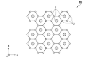
- FIG. 2 is an example of the crystal structure of the substance M1 constituting the optical switch element according to the first embodiment.
- FIG. 2 shows a crystal structure of ⁇ -RuCl 3 as an example of the substance M1.
- the optical switch element 10 includes a substance M1 having a plurality of transition metal elements 1 and a plurality of anions 2.
- the transition metal element 1 may have electrons in the d-orbital.
- the transition metal element 1 has, for example, an electron in the 4d orbital, and is, for example, Y, Zr, Nb, Mo, Tc, Ru, Rh, Pd, Ag, and Cd.
- the transition metal element 1 in FIG. 2 is Ru.
- the plurality of transition metal elements 1 are arranged in a lattice pattern.
- the arrangement of the plurality of transition metal elements 1 is, for example, arranged in a two-dimensional lattice pattern. Specifically, the arrangement of the plurality of transition metal elements 1 may be, for example, one of a honeycomb lattice shape, a triangular lattice pattern, and a kagome lattice pattern.
- the shape of the unit lattice of the two-dimensional lattice may be a triangle, a quadrangle (square, rectangle, parallelogram, rhombus), a hexagon or the like. It is particularly preferable that the arrangement of the plurality of transition metal elements 1 is honeycomb-shaped. The transition metal element 1 in FIG. 2 is connected in a honeycomb lattice pattern.
- the plurality of anions 2 surround each transition metal element 1.
- the plurality of anions 2 are arranged in a lattice pattern, and the transition metal element 1 is contained at the center position of the lattice.
- the arrangement of the anions 2 is, for example, a honeycomb lattice pattern, a triangular lattice pattern, a kagome lattice pattern, and preferably a honeycomb lattice pattern.
- the anion 2 is, for example, a chloride ion (Cl ⁇ ) or an oxide ion (O 2- ).
- the anion 2 in FIG. 2 is Cl ⁇ .
- the substance M1 used in the optical switch element 10 is, for example, ⁇ -RuCl 3 , Na 2 IrO 3 , Li 2 IrO 3 , Bi 3 Mn 4 O 12 (NO 3 ), ZnCu 3 (OH 6 Cl 2 ), and a transition metal. It is a chalcogenide.
- FIG. 3 shows an example of the positional relationship between one transition metal element 1 in a substance and the surrounding anion 2.
- FIG. 3 is a schematic diagram for explaining crystal field splitting.
- the anion 2 is located at the apex position of the octahedron centered on the transition metal element 1.
- crystal field splitting of the d-orbital occurs.
- the d-orbital of the transition metal element 1 that has been degenerate quintuple is split into an eg orbital that is degenerate twice and a t 2g orbital that is degenerate triple due to the octahedral crystal field created by the p-orbital of the anion 2 . do.
- the t 2g orbital has three orbital degrees of freedom of d xy , d yz , and d z x .
- the d- orbital becomes an eg orbital due to crystal field splitting. It is divided into t 2g orbitals.
- FIG. 4 shows the distribution of the t 2g orbital in which the d orbital of the transition metal element 1 is split.
- the t 2g orbitals in which the d orbitals of the transition metal element 1 are split are connected in a lattice pattern along the arrangement of the transition metal element 1. It is preferable that the t 2g orbitals are connected in a honeycomb lattice shape, a triangular lattice pattern, and a kagome lattice pattern, and the t 2g orbitals are connected in a honeycomb lattice pattern, for example.
- the t 2g orbitals connected in a grid pattern are composed of a unit structure of a plurality of t 2g orbitals connected in a ring shape.
- the unit structure of the t 2g orbitals connected in an annular shape is a hexagon.
- the t 2g orbitals are connected means that the electrons in the t 2g orbitals of one transition metal element 1 can propagate to the t 2g orbitals of another transition metal element 1, and the electron clouds of each d orbital are completely connected. It is not limited to the case where. For example, the case where the electron of the t 2g orbital of one transition metal element 1 hopping propagates to the t 2g orbital of another transition metal element 1 is included.
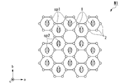
- the substance M1 does not have long-range order of spin (long-range magnetic order) in a temperature range above the Néel temperature TN , for example.
- the substance M1 may be, for example, a quantum spin liquid having no long-range order of spins but having short-range order, and may have neither long-range order nor short-range order of spins.
- sp2 and sp2 show antiferromagnetic order (long-range order) arranged in a zigzag pattern, they do not have magnetic order (long-range order) in the temperature range above the Néel temperature TN .
- the optical switch element 10 is irradiated with the signal light L1.
- the signal light L1 passes through the optical switch element 10 and reaches the polarizing plate 40.
- the optical switch element 10 is not irradiated with the control light C1, the polarization state of the signal light L1 does not change.
- the optical switch element 10 is irradiated with the circularly polarized control light C1.
- the wavelength of the control light C1 is, for example, preferably 1 ⁇ m or more, and more preferably 1.2 ⁇ m or more.
- the efficiency of rotating the polarization direction is higher than when the wavelength of the control light C1 is visible light.
- the angle between the signal light L2 and the signal light L1 is referred to as a rotation angle ⁇ .
- the direction of polarization rotation changes depending on the helicity of circular polarization (clockwise ⁇ + , counterclockwise ⁇ ⁇ ).
- clockwise ⁇ + When the helicity of circular polarization is clockwise ⁇ + , it rotates counterclockwise, and when the helicity of circular polarization is counterclockwise ⁇ ⁇ , it rotates clockwise.
- the rotation angle ⁇ changes according to the thickness of the optical switching element 10 in the z direction and the intensity of the control light C1.
- the thickness of the optical switching element 10 in the z direction is large, the rotation angle ⁇ becomes large.
- the intensity of the control light C1 is strong, the rotation angle ⁇ of the optical switching element 10 becomes large.
- the optical switch device 100 performs a switching operation, for example, "ON" when the amount of transmitted light is equal to or greater than the threshold value and "OFF" when the amount of light transmitted is equal to or less than the threshold value.
- the optical switch device 100 generates orbital angular momentum by transitioning the excited electrons so as to twist in a ring shape between orbitals having different degrees of freedom, and rotates the polarization direction of the signal light L1.
- This principle is different from the conventional magneto-optical effect using the inverse Faraday effect, and is expressed even in a state (phase) without long-distance magnetic order. That is, the optical switch device 100 according to the first embodiment can perform the optical switch operation by the control light C1 regardless of the Neel temperature TN .
- the optical switch device 100 Since the optical magnetic switch utilizing the reverse Faraday effect operates only at a nail temperature of less than TN in principle, the optical switch device 100 according to the first embodiment operating at a Néel temperature of TN or higher operates according to a new principle. It can be said that it is.
- the optical switch device 100 according to the first embodiment can be used for an optical communication system, an optical computer, and the like.
- FIG. 6 is a block diagram of the optical communication system 200 according to the first embodiment.
- the optical communication system 200 has a plurality of transmission / reception devices 110.
- Each of the transmission / reception devices 110 has a transmission device 101 and a reception device 102.
- the transmission device 101 includes a signal generation unit 50 and an optical switch device 100.
- the receiving device 102 includes a photoelectric conversion element 60 and a signal processing element 70.
- the signal generation unit 50 generates a digital signal.
- the control element 30 irradiates the optical switch element 10 with the control light C1 based on the signal input from the signal generation unit 50.
- the optical switch element 10 rotates the polarization direction of the signal light L1 emitted from the light source 20 according to the control light C1.
- the optical switch device 100 emits light having different intensities depending on the degree of coincidence between the polarization direction through which the polarizing plate 40 can pass and the polarization direction of the signal light. That is, the transmission device 101 converts the digital signal (for example, "1" 0 "" 1 "" 0 ”) generated by the signal generation unit 50 into an optical signal (for example,” ON “OFF” "ON” "OFF”). replace.
- the receiving device 102 receives the optical signal emitted from the transmitting device 101.
- the optical signal is replaced with an electric signal by the photoelectric conversion element 60, and is processed by the signal processing element 70.
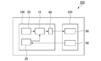
- FIG. 7 is a block diagram of the optical computer 300 according to the first embodiment.
- the optical computer 300 has, for example, an optical switch device 100 and an integrated circuit 120.
- the integrated circuit 120 has a storage unit 80 and a signal processing unit 90.
- the information recorded in the storage unit 80 is sent to the control element 30.
- the control element 30 irradiates the control light C1 based on the information stored in the storage unit 80.
- the signal processing unit 90 performs processing based on the optical signal emitted from the optical switch device 100.
- FIG. 8 is a perspective view of the optical switch device 100A according to the first modification.
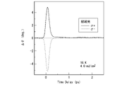
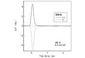
- Example 1 Using ⁇ -RuCl 3 as the optical switch element 10, the polarization rotation of light was verified. The thickness of the optical switching element 10 in the z direction was set to 50 ⁇ m. In Example 1, the optical switch element 10 was irradiated with circularly polarized light, and the light transmitted through the optical switch element 10 was measured. Then, the rotation angle ⁇ between the polarization direction of the incident light on the optical switch element 10 and the polarization direction of the emitted light was obtained.
- a circularly polarized pulse having an intensity of 4.0 mJ / cm 2 and a pulse width of 200 fsec was used as the control light C1 incident on the optical switch element 10.
- the photon energy of the circularly polarized pulse was 0.89 eV (wavelength 1.4 ⁇ m). Circularly polarized helicity was performed for clockwise ⁇ + and counterclockwise ⁇ -, respectively.
- the signal light L1 to be applied to the optical switch element 10 is a linearly polarized probe light.
- the photon energy of the signal light L1 was 0.62 eV (wavelength 2.0 ⁇ m).
- the measurement temperature was 16K.
- FIG. 9 shows the time change of the polarization rotation due to the circular polarization excitation in the optical switch element of the first embodiment.
- the rotation angle ⁇ of the polarization rotation was 4 degrees or more.
- the direction of rotation of the polarization rotation depended on the helicity of the circular polarization.
- the optical switch element 10 can rotate the signal light L1 by polarization, and the optical switch device 100 functions by inserting a polarizing plate into the optical path of the light emitted from the optical switch element 10. Further, since the optical switch element 10 operates with a pulse width in femtosecond units, the optical switch device 100 can also support high-speed communication.
- Example 2 is different from Example 1 in that the measurement temperature is 295 K. Other conditions were examined in the same manner as in Example 1.
- FIG. 10 shows the time change of the polarization rotation due to the circular polarization excitation in the optical switch element of the second embodiment. The same result as in Example 1 was shown in Example 2. As shown in Example 2, it was confirmed that the optical switch element operates even at room temperature.
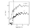
- Example 3 is different from Example 1 in that the temperature dependence of the maximum value of the rotation angle ⁇ of the polarization rotation by circular polarization excitation is measured by changing the measurement temperature. Other conditions were examined in the same manner as in Example 1.
- FIG. 11 shows the measurement results of Example 3.
- polarization rotation by ⁇ -RuCl 3 occurred at any temperature.
- ⁇ -RuCl 3 had a Neel temperature of TN or higher, and the rotation angle ⁇ of the polarization rotation was large. That is, it can be said that the long-distance magnetic order in the in-plane direction as shown in FIG. 5 hinders the rotation of the polarized light.
- the polarization rotation occurs when the Néel temperature is less than TN , and the polarization rotation does not occur when the Néel temperature is TN or more. Therefore, it can be said that the phenomenon shown in FIG. 11 is the opposite behavior of the magneto-optical switch utilizing the conventional reverse Faraday effect, and that the polarization rotation is caused by a different principle.
- Example 4 the mechanism of generation of photoinduced magnetization in ⁇ -RuCl 3 was investigated by theoretical analysis considering the quantum many-body effect. Specifically, there are on-site electron-electron interactions and spin-orbit interactions between the t 2g orbitals (d yz , d xx, d xy orbitals ) of the honeycomb lattice as shown in FIG. 4, and the transfer integrals are closest to each other. We dealt with the case of the site only. Numerical calculations were performed by the exact diagonalization method for a 6-site periodic system with 3-fold symmetry. In the numerical calculation, the light irradiation effect on the electronic state obtained by the exact diagonalization method was performed by the time-dependent Schrodinger equation. Photoexcitation was introduced as the Peierls phase, and the excitation energy was set to be equal to or less than the motto gap equivalent to that of Example 1.
- FIG. 12 shows the time change of the plane component of the magnetization generated in ⁇ -RuCl 3 by the circular polarization excitation obtained by the theoretical calculation of Example 4.
- the magnetization of this plane component is that the excited electrons make hopping transitions while twisting the orbitals with different degrees of freedom in a ring shape between each site of the honeycomb lattice (for example, d xy ⁇ d yz ⁇ d z x ⁇ d xy ). It turned out to occur in.
- Example 5 is different from Example 1 in that the behavior of polarization rotation due to circular polarization excitation is measured by changing the wavelengths of the signal light L1 and the control light C1.
- FIG. 13 shows the measurement results of Example 5.
- FIG. 13A shows the absorption wavelength of ⁇ -RuCl 3 (optical switching element 10).
- FIG. 13 (a) is based on FIGS. 1 (a) and 4 (a) of L. J. Sandilands et al., Phys. Rev. B 93, 075144 (2016). Both the solid line graph and the dotted line graph shown in FIG. 13 (a) show the absorption of ⁇ -RuCl 3 .
- the dotted line graph is a 25-fold magnified view of the solid line graph in the region where the photon energy is 1.0 eV or less (wavelength 1.24 ⁇ m or more).
- FIGS. 13B to 13 (d) show changes in the rotation angle ⁇ when the optical switching element 10 is irradiated with the control light C1 having different photon energies ( Epu ).
- FIG. 13B is a result when the photon energy of the control light C1 is 0.3 eV (wavelength 3.8 ⁇ m).
- FIG. 13 (c) shows the results when the photon energy of the control light C1 is 0.62 eV (wavelength 2.0 ⁇ m).
- FIG. 13D shows the results when the photon energy of the control light C1 is 0.89 eV (wavelength 1.4 ⁇ m).
- the horizontal axis of FIGS. 13B to 13D is the photon energy of the signal light L1, and the vertical axis is the rotation angle ⁇ .
- As the control light C1 a circularly polarized pulse having an intensity of 1.0 mJ / cm 2 and a pulse width of 200 fsec was used.
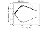
- FIG. 14 shows the time change of the rotation angle ⁇ in the polarization direction when the photon energy of the control light C1 is changed to 1.55 eV (wavelength 800 nm).
- ⁇ -RuCl 3 absorbs light more in the region where the photon energy is 1.55 eV than in the region where the photon energy is 1.0 eV or less (see (a) in FIG. 13).
- FIG. 14A shows the result of setting the photon energy of the signal light L1 to 0.54 eV (wavelength 2.3 ⁇ m), and FIG. 14B shows the photon energy of the signal light L1 set to 1.03 eV (wavelength 1.2 ⁇ m). It is the result of doing.
- the horizontal axis of FIG. 14 is the elapsed time after irradiation with the control light C1, and the vertical axis is the rotation angle ⁇ .
- As the control light C1 a circularly polarized pulse having an intensity of 1.0 mJ / cm 2 and a pulse width of 200 fsec was used.
- the rotation angle ⁇ changed by irradiating the control light C1.
- the rotation angle was smaller than the experimental results (FIGS. 13 (b) to (d)) in the region where the photon energy was 1.0 eV or less.
- Optical switch element 1 ... Transition metal element, 2 ... Anion, 10 ... Optical switch element, 20 ... Light source, 30 ... Control element, 40 ... Plate plate, 50 ... Signal generator, 60 ... Photoelectric conversion element, 70 ... Signal processing element, 80 ... Storage unit, 90 ... Signal processing unit, 100, 100A ... Optical switch device, 101 ... Transmission device, 102 ... Receiver device, 110 ... Transmission / reception device, 120 ... Integrated circuit, 200 ... Optical communication system, 300 ... Optical computer, C1 ... control light, L1, L2 ... signal light, sp1 ... first spin, sp2 ... second spin, ⁇ ... rotation angle
Landscapes
- Physics & Mathematics (AREA)
- Nonlinear Science (AREA)
- Engineering & Computer Science (AREA)
- Power Engineering (AREA)
- General Physics & Mathematics (AREA)
- Optics & Photonics (AREA)
- Computer Networks & Wireless Communication (AREA)
- Optical Modulation, Optical Deflection, Nonlinear Optics, Optical Demodulation, Optical Logic Elements (AREA)
Abstract
Description
光スイッチ素子10として、α-RuCl3を用いて、光の偏光回転を検証した。光スイッチング素子10のz方向の厚みは、50μmとした。実施例1では、光スイッチ素子10に円偏光光を照射し、光スイッチ素子10を透過して出射する光を測定した。そして、光スイッチ素子10への入射光の偏光方向と出射光の偏光方向との回転角度θを求めた。
実施例2は、測定温度を295Kとした点が実施例1と異なる。その他の条件は、実施例1と同様の検討を行った。図10は、実施例2の光スイッチ素子における円偏光励起による偏光回転の時間変化を示す。実施例2においても実施例1と同様の結果が示された。実施例2に示すように、光スイッチ素子は室温でも動作することが確認された。
実施例3では、測定温度を変えて、円偏光励起による偏光回転の回転角度θの最大値の温度依存性を測定した点が、実施例1と異なる。その他の条件は、実施例1と同様の検討を行った。図11は、実施例3の測定結果を示す。
実施例4では、量子多体効果を考慮した理論解析によって、α-RuCl3における光誘起磁化の発生機構を検討した。具体的には、図4に示すようなハニカム格子のt2g軌道(dyz、dxz、dxy軌道)間にオンサイトの電子間相互作用とスピン軌道相互作用があり、トランスファー積分が最近接サイトのみの場合を扱った。3回対称性を有する6サイトの周期系に対して、厳密対角化法による数値計算を行った。数値計算は、厳密対角化法によって得た電子状態に対する光照射効果を時間依存シュレーディンガー方程式によって行った。光励起は、パイエルス位相として導入し、励起エネルギーは実施例1と同等のモットギャップ以下とした。
実施例5は、信号光L1及び制御光C1の波長を変えて、円偏光励起による偏光回転の挙動を測定した点が、実施例1と異なる。
Claims (7)
- d軌道に電子を有する複数の遷移金属元素と、前記複数の遷移金属元素のそれぞれの周囲に配置された複数の陰イオンと、を有する物質を含み、
前記複数の遷移金属元素は格子状に配列し、前記複数の遷移金属元素のそれぞれのd軌道が分裂したt2g軌道は環状に繋がり、
前記物質が長距離の磁気秩序を持たない状態で、制御光が照射された際に信号光を偏光回転させる、光スイッチ素子。 - 前記複数の遷移金属元素の配列がハニカム格子状、三角格子状、カゴメ格子状のいずれかである、請求項1に記載の光スイッチ素子。
- 前記物質がα-RuCl3である、請求項1又は2に記載の光スイッチ素子。
- 前記制御光の波長が1μm以上である、請求項1~3のいずれか一項に記載の光スイッチ素子。
- 請求項1~4のいずれか一項に記載の光スイッチ素子と、
前記光スイッチ素子に前記信号光を照射する光源と、
前記光スイッチ素子に前記制御光を照射する制御素子と、
前記光スイッチ素子を透過又は反射した光を偏光する偏光板と、を有する、光スイッチ装置。 - 請求項5に記載の光スイッチ装置を備える、光通信システム。
- 請求項5に記載の光スイッチ装置を備える、光コンピュータ。
Priority Applications (3)
| Application Number | Priority Date | Filing Date | Title |
|---|---|---|---|
| DE112021006363.4T DE112021006363T5 (de) | 2020-12-08 | 2021-12-02 | Optisches schalterelement, optische schaltervorrichtung, optisches kommunikationssystem und optische rechenvorrichtung |
| JP2022568239A JPWO2022124205A1 (ja) | 2020-12-08 | 2021-12-02 | |
| US18/265,360 US20240111181A1 (en) | 2020-12-08 | 2021-12-02 | Optical switch element, optical switch device, optical communication system, and optical computer |
Applications Claiming Priority (2)
| Application Number | Priority Date | Filing Date | Title |
|---|---|---|---|
| JP2020203352 | 2020-12-08 | ||
| JP2020-203352 | 2020-12-08 |
Publications (1)
| Publication Number | Publication Date |
|---|---|
| WO2022124205A1 true WO2022124205A1 (ja) | 2022-06-16 |
Family
ID=81973222
Family Applications (1)
| Application Number | Title | Priority Date | Filing Date |
|---|---|---|---|
| PCT/JP2021/044368 Ceased WO2022124205A1 (ja) | 2020-12-08 | 2021-12-02 | 光スイッチ素子、光スイッチ装置、光通信システム及び光コンピュータ |
Country Status (4)
| Country | Link |
|---|---|
| US (1) | US20240111181A1 (ja) |
| JP (1) | JPWO2022124205A1 (ja) |
| DE (1) | DE112021006363T5 (ja) |
| WO (1) | WO2022124205A1 (ja) |
Citations (2)
| Publication number | Priority date | Publication date | Assignee | Title |
|---|---|---|---|---|
| JPH09146058A (ja) * | 1995-11-22 | 1997-06-06 | Fuji Electric Co Ltd | 光スイッチ |
| JP2008135480A (ja) * | 2006-11-27 | 2008-06-12 | Osaka Univ | 磁性制御方法 |
Family Cites Families (1)
| Publication number | Priority date | Publication date | Assignee | Title |
|---|---|---|---|---|
| JP5732194B2 (ja) | 2006-05-24 | 2015-06-10 | スティッチング カソリーケ ウニベルシテイト | 磁化可能な媒体を切り替える光磁気スイッチング素子および方法 |
-
2021
- 2021-12-02 DE DE112021006363.4T patent/DE112021006363T5/de active Pending
- 2021-12-02 JP JP2022568239A patent/JPWO2022124205A1/ja active Pending
- 2021-12-02 US US18/265,360 patent/US20240111181A1/en active Pending
- 2021-12-02 WO PCT/JP2021/044368 patent/WO2022124205A1/ja not_active Ceased
Patent Citations (2)
| Publication number | Priority date | Publication date | Assignee | Title |
|---|---|---|---|---|
| JPH09146058A (ja) * | 1995-11-22 | 1997-06-06 | Fuji Electric Co Ltd | 光スイッチ |
| JP2008135480A (ja) * | 2006-11-27 | 2008-06-12 | Osaka Univ | 磁性制御方法 |
Non-Patent Citations (2)
| Title |
|---|
| HIROBE DAICHI, SATO MASAHIRO, SHIOMI YUKI, TANAKA HIDEKAZU, SAITOH EIJI: "Magnetic thermal conductivity far above the Neel temperature in the Kitaev-magnet candidate α-RuCl3", PHYSICAL REVIEW B, vol. 95, no. 24, 22 June 2017 (2017-06-22), pages 241112 - 241112-6, XP055942667, ISSN: 2469-9950, DOI: 10.1103/PhysRevB.95.241112 * |
| TATSUYA AMANO A, CHUO, AMANO, AKAMINE Y, OHASHI H, KAWAKAMI Y, ITOH H, KONNO K, HASEGAWA Y, SASAKI K, AOYAMA T, IMAI Y, OHGUSHI K: "18pE25-4 : II Ultrafast spin dynamics of Kitaev spin liquid candidate α-RuCl3 II", MEETING ABSTRACTS OF THE PHYSICAL SOCIETY OF JAPAN, PHYSICAL SOCIETY OF JAPAN, JP, 23 March 2020 (2020-03-23), JP , pages 1365, XP055942662, ISSN: 2189-0803 * |
Also Published As
| Publication number | Publication date |
|---|---|
| US20240111181A1 (en) | 2024-04-04 |
| JPWO2022124205A1 (ja) | 2022-06-16 |
| DE112021006363T5 (de) | 2023-10-05 |
Similar Documents
| Publication | Publication Date | Title |
|---|---|---|
| Murakami et al. | Resonant x-ray scattering from orbital ordering in LaMnO 3 | |
| Inami et al. | Orbital excitations in LaMnO 3 studied by resonant inelastic x-ray scattering | |
| Fischer et al. | X-rays and magnetism | |
| Chen et al. | Skyrmion based magnonic crystals | |
| Meskine et al. | Orbital ordering and exchange interaction in the manganites | |
| Karpov et al. | Nanoscale topological defects and improper ferroelectric domains in multiferroic barium hexaferrite nanocrystals | |
| Moskvin et al. | Optical spectroscopy of charge transfer transitions in multiferroic manganites, ferrites, and related insulators | |
| Fogh et al. | Randomness and frustration in a S= 1 2 square-lattice Heisenberg antiferromagnet | |
| Tusche et al. | Low-energy spin-polarized electrons: their role in surface physics | |
| Frawley et al. | Elucidation of the helical spin structure of FeAs | |
| WO2022124205A1 (ja) | 光スイッチ素子、光スイッチ装置、光通信システム及び光コンピュータ | |
| Zhang et al. | Bulk photovoltaic effects in helimagnets | |
| Singh | Solid state physics | |
| Porter et al. | Guiding antiferromagnetic transitions in Ca 2 RuO 4 | |
| Magnuson et al. | Large magnetic circular dichroism in resonant inelastic x-ray scattering at the Mn L-edge of Mn-Zn ferrite | |
| Lovesey | Orthoferrite with a hidden lanthanide magnetic motif: NdFeO 3 | |
| Walker et al. | X-ray resonant scattering study of the structural and magnetic transitions in PrB 6 | |
| Abramova et al. | Ultrasmall-angle X-ray scattering analysis of photonic crystal structure | |
| Katsumata | Synchrotron x-ray diffraction studies of magnetic materials under extreme conditions | |
| Hayashi et al. | Local spin ordering in the antiferromagnetic as well as paramagnetic La Mn O 3 phase revealed by polarized spin-selected 1 s→ 3 d absorption spectra | |
| Lovesey | EuPdSn2: magnetic structures in view of resonant X-ray Bragg diffraction | |
| Da Pieve et al. | Real-space Green's function approach to angle-resolved resonant photoemission: Spin polarization and circular dichroism in itinerant magnets | |
| Radaelli et al. | The contribution of Diamond Light Source to the study of strongly correlated electron systems and complex magnetic structures | |
| Flores | Scaling, stability range, magnetic excitations and light-induced effects in Cu2OSeO3 | |
| Takubo et al. | 6-GHz lattice response in a quantum spin-orbital liquid probed by time-resolved resonant x-ray scattering |
Legal Events
| Date | Code | Title | Description |
|---|---|---|---|
| 121 | Ep: the epo has been informed by wipo that ep was designated in this application |
Ref document number: 21903309 Country of ref document: EP Kind code of ref document: A1 |
|
| ENP | Entry into the national phase |
Ref document number: 2022568239 Country of ref document: JP Kind code of ref document: A |
|
| WWE | Wipo information: entry into national phase |
Ref document number: 18265360 Country of ref document: US |
|
| WWE | Wipo information: entry into national phase |
Ref document number: 112021006363 Country of ref document: DE |
|
| 122 | Ep: pct application non-entry in european phase |
Ref document number: 21903309 Country of ref document: EP Kind code of ref document: A1 |