WO2022124019A1 - フォトディテクタ、フォトディテクタアレイおよび距離測定システム - Google Patents
フォトディテクタ、フォトディテクタアレイおよび距離測定システム Download PDFInfo
- Publication number
- WO2022124019A1 WO2022124019A1 PCT/JP2021/041947 JP2021041947W WO2022124019A1 WO 2022124019 A1 WO2022124019 A1 WO 2022124019A1 JP 2021041947 W JP2021041947 W JP 2021041947W WO 2022124019 A1 WO2022124019 A1 WO 2022124019A1
- Authority
- WO
- WIPO (PCT)
- Prior art keywords
- spad
- transistor
- photodetector
- resistance
- resistor
- Prior art date
- Legal status (The legal status is an assumption and is not a legal conclusion. Google has not performed a legal analysis and makes no representation as to the accuracy of the status listed.)
- Ceased
Links
Images


Classifications
-
- G—PHYSICS
- G01—MEASURING; TESTING
- G01S—RADIO DIRECTION-FINDING; RADIO NAVIGATION; DETERMINING DISTANCE OR VELOCITY BY USE OF RADIO WAVES; LOCATING OR PRESENCE-DETECTING BY USE OF THE REFLECTION OR RERADIATION OF RADIO WAVES; ANALOGOUS ARRANGEMENTS USING OTHER WAVES
- G01S17/00—Systems using the reflection or reradiation of electromagnetic waves other than radio waves, e.g. lidar systems
- G01S17/02—Systems using the reflection of electromagnetic waves other than radio waves
- G01S17/06—Systems determining position data of a target
- G01S17/08—Systems determining position data of a target for measuring distance only
- G01S17/10—Systems determining position data of a target for measuring distance only using transmission of interrupted, pulse-modulated waves
-
- G—PHYSICS
- G01—MEASURING; TESTING
- G01S—RADIO DIRECTION-FINDING; RADIO NAVIGATION; DETERMINING DISTANCE OR VELOCITY BY USE OF RADIO WAVES; LOCATING OR PRESENCE-DETECTING BY USE OF THE REFLECTION OR RERADIATION OF RADIO WAVES; ANALOGOUS ARRANGEMENTS USING OTHER WAVES
- G01S7/00—Details of systems according to groups G01S13/00, G01S15/00, G01S17/00
- G01S7/48—Details of systems according to groups G01S13/00, G01S15/00, G01S17/00 of systems according to group G01S17/00
- G01S7/481—Constructional features, e.g. arrangements of optical elements
- G01S7/4816—Constructional features, e.g. arrangements of optical elements of receivers alone
-
- G—PHYSICS
- G01—MEASURING; TESTING
- G01S—RADIO DIRECTION-FINDING; RADIO NAVIGATION; DETERMINING DISTANCE OR VELOCITY BY USE OF RADIO WAVES; LOCATING OR PRESENCE-DETECTING BY USE OF THE REFLECTION OR RERADIATION OF RADIO WAVES; ANALOGOUS ARRANGEMENTS USING OTHER WAVES
- G01S7/00—Details of systems according to groups G01S13/00, G01S15/00, G01S17/00
- G01S7/48—Details of systems according to groups G01S13/00, G01S15/00, G01S17/00 of systems according to group G01S17/00
- G01S7/483—Details of pulse systems
- G01S7/486—Receivers
- G01S7/4861—Circuits for detection, sampling, integration or read-out
- G01S7/4863—Detector arrays, e.g. charge-transfer gates
-
- H—ELECTRICITY
- H10—SEMICONDUCTOR DEVICES; ELECTRIC SOLID-STATE DEVICES NOT OTHERWISE PROVIDED FOR
- H10F—INORGANIC SEMICONDUCTOR DEVICES SENSITIVE TO INFRARED RADIATION, LIGHT, ELECTROMAGNETIC RADIATION OF SHORTER WAVELENGTH OR CORPUSCULAR RADIATION
- H10F30/00—Individual radiation-sensitive semiconductor devices in which radiation controls the flow of current through the devices, e.g. photodetectors
- H10F30/20—Individual radiation-sensitive semiconductor devices in which radiation controls the flow of current through the devices, e.g. photodetectors the devices having potential barriers, e.g. phototransistors
- H10F30/21—Individual radiation-sensitive semiconductor devices in which radiation controls the flow of current through the devices, e.g. photodetectors the devices having potential barriers, e.g. phototransistors the devices being sensitive to infrared, visible or ultraviolet radiation
- H10F30/22—Individual radiation-sensitive semiconductor devices in which radiation controls the flow of current through the devices, e.g. photodetectors the devices having potential barriers, e.g. phototransistors the devices being sensitive to infrared, visible or ultraviolet radiation the devices having only one potential barrier, e.g. photodiodes
- H10F30/225—Individual radiation-sensitive semiconductor devices in which radiation controls the flow of current through the devices, e.g. photodetectors the devices having potential barriers, e.g. phototransistors the devices being sensitive to infrared, visible or ultraviolet radiation the devices having only one potential barrier, e.g. photodiodes the potential barrier working in avalanche mode, e.g. avalanche photodiodes
-
- H—ELECTRICITY
- H10—SEMICONDUCTOR DEVICES; ELECTRIC SOLID-STATE DEVICES NOT OTHERWISE PROVIDED FOR
- H10F—INORGANIC SEMICONDUCTOR DEVICES SENSITIVE TO INFRARED RADIATION, LIGHT, ELECTROMAGNETIC RADIATION OF SHORTER WAVELENGTH OR CORPUSCULAR RADIATION
- H10F39/00—Integrated devices, or assemblies of multiple devices, comprising at least one element covered by group H10F30/00, e.g. radiation detectors comprising photodiode arrays
- H10F39/10—Integrated devices
- H10F39/103—Integrated devices the at least one element covered by H10F30/00 having potential barriers, e.g. integrated devices comprising photodiodes or phototransistors
-
- H—ELECTRICITY
- H10—SEMICONDUCTOR DEVICES; ELECTRIC SOLID-STATE DEVICES NOT OTHERWISE PROVIDED FOR
- H10F—INORGANIC SEMICONDUCTOR DEVICES SENSITIVE TO INFRARED RADIATION, LIGHT, ELECTROMAGNETIC RADIATION OF SHORTER WAVELENGTH OR CORPUSCULAR RADIATION
- H10F39/00—Integrated devices, or assemblies of multiple devices, comprising at least one element covered by group H10F30/00, e.g. radiation detectors comprising photodiode arrays
- H10F39/10—Integrated devices
- H10F39/107—Integrated devices having multiple elements covered by H10F30/00 in a repetitive configuration, e.g. radiation detectors comprising photodiode arrays
-
- H—ELECTRICITY
- H10—SEMICONDUCTOR DEVICES; ELECTRIC SOLID-STATE DEVICES NOT OTHERWISE PROVIDED FOR
- H10F—INORGANIC SEMICONDUCTOR DEVICES SENSITIVE TO INFRARED RADIATION, LIGHT, ELECTROMAGNETIC RADIATION OF SHORTER WAVELENGTH OR CORPUSCULAR RADIATION
- H10F39/00—Integrated devices, or assemblies of multiple devices, comprising at least one element covered by group H10F30/00, e.g. radiation detectors comprising photodiode arrays
- H10F39/10—Integrated devices
- H10F39/12—Image sensors
- H10F39/18—Complementary metal-oxide-semiconductor [CMOS] image sensors; Photodiode array image sensors
- H10F39/182—Colour image sensors
-
- H—ELECTRICITY
- H10—SEMICONDUCTOR DEVICES; ELECTRIC SOLID-STATE DEVICES NOT OTHERWISE PROVIDED FOR
- H10F—INORGANIC SEMICONDUCTOR DEVICES SENSITIVE TO INFRARED RADIATION, LIGHT, ELECTROMAGNETIC RADIATION OF SHORTER WAVELENGTH OR CORPUSCULAR RADIATION
- H10F39/00—Integrated devices, or assemblies of multiple devices, comprising at least one element covered by group H10F30/00, e.g. radiation detectors comprising photodiode arrays
- H10F39/80—Constructional details of image sensors
- H10F39/803—Pixels having integrated switching, control, storage or amplification elements
- H10F39/8037—Pixels having integrated switching, control, storage or amplification elements the integrated elements comprising a transistor
- H10F39/80377—Pixels having integrated switching, control, storage or amplification elements the integrated elements comprising a transistor characterised by the channel of the transistor, e.g. channel having a doping gradient
-
- H—ELECTRICITY
- H10—SEMICONDUCTOR DEVICES; ELECTRIC SOLID-STATE DEVICES NOT OTHERWISE PROVIDED FOR
- H10F—INORGANIC SEMICONDUCTOR DEVICES SENSITIVE TO INFRARED RADIATION, LIGHT, ELECTROMAGNETIC RADIATION OF SHORTER WAVELENGTH OR CORPUSCULAR RADIATION
- H10F39/00—Integrated devices, or assemblies of multiple devices, comprising at least one element covered by group H10F30/00, e.g. radiation detectors comprising photodiode arrays
- H10F39/80—Constructional details of image sensors
- H10F39/811—Interconnections
-
- G—PHYSICS
- G01—MEASURING; TESTING
- G01S—RADIO DIRECTION-FINDING; RADIO NAVIGATION; DETERMINING DISTANCE OR VELOCITY BY USE OF RADIO WAVES; LOCATING OR PRESENCE-DETECTING BY USE OF THE REFLECTION OR RERADIATION OF RADIO WAVES; ANALOGOUS ARRANGEMENTS USING OTHER WAVES
- G01S17/00—Systems using the reflection or reradiation of electromagnetic waves other than radio waves, e.g. lidar systems
- G01S17/88—Lidar systems specially adapted for specific applications
- G01S17/89—Lidar systems specially adapted for specific applications for mapping or imaging
- G01S17/894—Three-dimensional [3D] imaging with simultaneous measurement of time-of-flight at a two-dimensional [2D] array of receiver pixels, e.g. time-of-flight cameras or flash lidar
Definitions
- the present disclosure relates to a photodetector, particularly a photodetector such as a solid-state image sensor capable of detecting weak light, a photodetector array, and a distance measurement system.
- SPAD Single Photon Avalanche Diode
- SPAD Single Photon Avalanche Diode
- SPAD is a photodiode whose light detection sensitivity is enhanced by multiplying the signal charge generated by photoelectric conversion by using the avalanche breakdown (or avalanche breakdown) phenomenon (Patent Document 1, Non-Patent Document 1). See ⁇ 5).
- the present disclosure is intended to provide a photodetector, a photodetector array and a distance measurement system that reduce the quenching dead time.
- the photodetector includes a single photon avalanche diode (hereinafter referred to as SPAD) and a first resistance connected in series with the SPAD, from the SPAD to the said. During the recharge time when the charge is discharged through the first resistance, the charge disappears from the multiplication region of the SPAD.
- SPAD photon avalanche diode
- the excess bias voltage applied to the SPAD is smaller than the breakdown voltage of the SPAD, and the resistance value R of the first resistor may satisfy the formula (21) described later.
- the photodetector array includes N of the above photodetectors (N is an integer of 2 or more), N series circuits included in the N photodetectors are connected in parallel, and the N series is connected in parallel.
- N is an integer of 2 or more
- N series circuits included in the N photodetectors are connected in parallel
- the N series is connected in parallel.
- Each of the series circuits has the SPAD and the first resistance connected in series, and one end of the N series circuits and the N ends on the SPAD side are connected to each other, and further, the above. It has a second resistance connected to the N end thereof connected to each other and connected in series with the N photodetectors, and the resistance value of the second resistance is N of the resistance value of the first resistance. Less than a fraction.
- the distance measuring measurement system includes a light receiving unit having a photodetector, a light emitting unit that emits light toward an object to be measured, and a control unit that controls the light receiving unit and the light emitting unit.
- the control unit receives a signal corresponding to the reflected light reflected by the measurement object from the light receiving unit and calculates the distance to the measurement object.
- the dead time of quenching can be shortened.
- FIG. 1A is a diagram showing a circuit example of a photodetector according to an embodiment.
- FIG. 1B is a diagram showing a list of physical quantities used in the simulation of FIG. 1A.
- FIG. 1C is a diagram showing a list of physical constants used in the simulation of FIG. 1A.
- FIG. 2 is a diagram showing the voltage fluctuation calculated from the simulation and the time change of the number of charges in the depletion layer.
- FIG. 3 is a diagram showing the time change of the reverse bias voltage when the avalanche multiplication occurs.
- FIG. 4 is a diagram showing a circuit example of the photodetector according to the first embodiment.
- FIG. 5 is a diagram showing a modified example of the photodetector according to the first embodiment.
- FIG. 1A is a diagram showing a circuit example of a photodetector according to an embodiment.
- FIG. 1B is a diagram showing a list of physical quantities used in the simulation of FIG. 1A.
- FIG. 6 is an example of a diagram showing whether or not quenching is possible with respect to the excess bias voltage and the resistance value of the first resistor.
- FIG. 7 is an example of a diagram showing whether or not quenching is possible with respect to the capacitance value of the first capacitance and the resistance value of the first resistor.
- FIG. 8 is a block diagram showing a configuration example of a control system including the photodetector according to the second embodiment.
- FIG. 9 is a block diagram showing another configuration example of the control system including the photodetector according to the second embodiment.
- FIG. 10 is a circuit diagram of a photodetector that realizes the control system of FIG. 8 or 9.
- FIG. 11 is a diagram showing a circuit example of the photodetector array according to the third embodiment.
- FIG. 12 is a diagram showing a circuit example of the solid-state image sensor according to the third embodiment.
- FIG. 13 is a diagram showing a layout example of the solid-state image sensor of FIG. 12A in a plan view.
- FIG. 14 is a diagram showing a modified example of the layout of the solid-state image sensor of FIG. 13 in a plan view.
- FIG. 15 is a diagram showing a cross-sectional configuration example of the solid-state image sensor in the XV-XV line of FIG.
- FIG. 16 is a diagram showing a modified example of the cross-sectional configuration of the solid-state image sensor in the XV-XV line of FIG.
- FIG. 17 is a diagram showing another cross-sectional configuration example of the solid-state image sensor according to the third embodiment.
- FIG. 13 is a diagram showing a layout example of the solid-state image sensor of FIG. 12A in a plan view.
- FIG. 14 is a diagram showing a modified example of the layout of the solid-state image sensor
- FIG. 18 is a schematic layout view of the entire solid-state image sensor of FIG. 17 as a plan view.
- FIG. 19 is a block diagram showing an example of a distance measurement system using a photodetector or a photodetector array according to the present disclosure.
- FIG. 20 is a diagram showing an example of a timing chart in the distance measurement measurement system of FIG.
- Non-Patent Document 1 in order to instantly stop the charge multiplication due to the avalanche breakdown of SPAD (quenching), a circuit element (quenching element or quenching resistance) such as a resistor or a transistor called a quenching element is used for SPAD.
- a circuit element quenching element or quenching resistance
- a configuration is presented that is connected in series with. Further, the simulation result is described, and the resistance value is described as 300 kohm on the 131st page.
- specific expressions and relationships with respect to the device structure of SPAD and circuit constants are not disclosed.
- Non-Patent Document 2 discloses a configuration that shortens the quenching dead time by controlling the reverse bias voltage across the SPAD according to the output from the SPAD.
- the quenching dead time refers to the time from the start of the avalanche multiplication to the return of the reverse bias voltage until the reverse bias voltage applied to the SPAD fluctuates until the multiplication can be performed again.
- the configuration for controlling the quenching resistance of the SPAD is not disclosed, and the resistance value required for the quenching resistance and the structure or characteristic value of the SPAD or the bias condition, specifically, the capacitance of the APD and the break No relationship has been shown between down voltage ( VBD ), depleted layer width, and excess bias voltage (Vex).
- Patent Document 1 presents a configuration in which the reverse bias voltage applied to the APD is controlled according to the current flowing through the APD, but the control of the quenching resistance, the capacitance of the APD, and the like is not shown.
- quenching is one of the operating principles of SPAD and refers to immediately stopping the avalanche multiplication at a constant magnification.
- a SPAD is an avalanche photodiode, which is an element used at a breakdown voltage or higher and capable of detecting electrons generated from a single photon by multiplying them by an avalanche multiplier.
- the present inventors have found from a dynamical simulation in quenching that the requirement for the quenching resistance of SPAD is "there is no carrier in the depletion layer in the process of quenching recharge", which will be described later. As shown in equation (21), the resistance condition was found.
- the resistance value of the quenching resistance can be set lower, or the quenching resistance can be actively controlled, and the quenching recharge time, that is, the dead time, can be shortened compared to the conventional SPAD. .. This makes it possible to improve the sensitivity of SPAD and expand the dynamic range.
- Simulation on which this disclosure is based First, the simulation on which the present disclosure is based will be described.
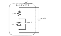
- FIG. 1A is a diagram showing a circuit example of the photodetector 1 according to the embodiment.
- a power supply 13 is shown in addition to the photodetector 1.
- This circuit example is a circuit diagram related to the simulation on which the present disclosure is based.
- the photodetector 1 includes a SPAD 10, a first resistor 11 connected in series to the anode of the SPAD 10, and a first capacitance 12 connected in parallel to the SPAD 10.
- the first resistor 11 is connected to the cathode side of the SPAD 10, but may be the anode side.
- a reverse bias voltage equal to or higher than the breakdown voltage is applied to the SPAD 10 at least in an idling state in which no electric charge is present in the depletion layer.
- the first capacitance 12 is the capacitance of the SPAD10 cathode and is a capacitance including the parasitic capacitance of SPAD10.
- the first capacity 12 contains parasitic components such as the junction capacity and the wiring capacity of the SPAD 10, does not need to be an external capacity, and the type is not limited.
- the first capacitance 12 is the sum of the parasitic capacitance of SPAD10 when there is no external capacitance, the parasitic capacitance of SPAD10 when there is an external capacitance, and the capacitance component parallel to SPAD10.
- the physical quantities used in the simulation are shown in FIG. 1B.
- the physical constants used in the simulation are shown in FIG. 1C.
- the physical constants with (* 1) in FIG. 1C refer to Non-Patent Document 3.
- the physical constants with (* 1) or (* 2) can take different values depending on the material, temperature, and the like.
- the physical constants with (* 3) are parameters that are set arbitrarily and are determined by the externally applied voltage, device structure, impurity concentration, and the like.
- this simulation and the physical constants in FIG. 1C assume silicon, the material is not limited and the material may be changed. In this case, the physical constant of FIG. 1C may be changed according to the material. Examples of other materials include materials such as germanium, gallium arsenide, gallium nitride, indium phosphide, and selenium.
- the electric charge generated by the avalanche multiplication is temporarily held in the first capacitance 12 and discharged to the power supply 13 via the first resistance 11. At this time, the voltage applied to both ends of the SPAD 10 and the magnitude of the internal electric field in the multiplying region in the SPAD 10 change according to the equations (5) to (7).
- Equation (8) shows the voltage fluctuation ⁇ V from the initial state.
- FIG. 2 is a diagram showing the voltage fluctuation calculated from the above simulation and the time change of the number of charges in the depletion layer.
- the vertical axis of FIGS. 2A and 2B shows the absolute value of the voltage fluctuation ⁇ V generated in the reverse bias voltage applied to the SPAD 10.
- the vertical axis of FIGS. 2C and 2 shows the number of electrons n in the depletion layer.
- the horizontal axis shows the time change.
- the charge generated by the avalanche multiplication accumulates in the capacitance, so that ⁇ V swings by about 2.6 V.
- the charge is discharged (recharged) through the resistor, so that ⁇ V decreases, becomes ⁇ V to 0.9V at t to 730 ns, and then increases again.
- ⁇ V continues the damped vibration and finally becomes 1.5V. Since ⁇ V does not return to 0, the avalanche multiplication has not stopped and quenching has not been possible.
- R 70 kohm of the first resistor 11
- ⁇ V decreases due to recharging
- the maximum value of the voltage amplitude in quenching of the photodetector of the present disclosure is larger than the surplus voltage Vex.
- the number of electrons n (t) in the depletion layer is always n (t) even while ⁇ V is decreasing due to recharging. Since it is 1 or more, the avalanche is multiplied again based on the electrons remaining in the depletion layer.
- the condition for realizing quenching in SPAD10 is that the carrier disappears from the depletion layer in the process of recharging, and quenching can be surely realized by setting the resistance value based on this condition. .. Further, by lowering the resistance value within the range satisfying this condition, the dead time can be shortened, the sensitivity can be improved, and the dynamic range can be expanded.
- the resistance value R of the first resistor 11 that satisfies the quenching condition that carriers disappear from the depletion layer in the process of recharging can be calculated analytically as follows.
- the impact ionization rate can be linearly approximated as in equations (9) and (10) when Vex is sufficiently small with respect to VBD .
- Non-Patent Document 5 it is known from Non-Patent Document 5 that the equations (12) and (13) are established in VBD .
- equations (1) and (2) can be rewritten as follows.
- FIG. 3 is a diagram showing a time change of the reverse bias voltage V when an avalanche multiplication occurs.
- the requirements for the resistance value R of the first resistance 11 are as follows.
- the condition of the equation (19) is almost the same as the time from the start of the avalanche multiplication to the time when all the charges are discharged is shorter than the time until the voltage is returned by the recharge.
- the resistance value R calculated by substituting the physical constant of FIG. 1C on the right side of the equation (21) is 68 kohms, which is consistent with the result of FIG.
- the dead time obtained from the equation (21) is RC, which is the recharge time due to the first resistance 11. Is. According to this, the dead time depends on (i) the surplus bias voltage Vex, (ii) the capacity C of the first capacity 12, (iii) the depletion layer width W, and (iv) the breakdown voltage VBD .
- the dead time can be further shortened by increasing Vex.
- the resistance value R of the first resistance 11 as the quenching resistance obtained from this simulation, the dead time can be reduced to 2 ns in the example of FIG. 2, for example.
- the dead time that is, the period described as Re-charge is about 300 ns.
- the dead time can be reduced to 1/100 or less.
- Non-Patent Document 4 the impact ionization rate in Non-Patent Document 4 is as shown in the following formula (9-1).
- the requirements to be satisfied by the resistance value R of the first resistance 11 as the quenching resistance may differ depending on the reference document, and are not limited by the temperature, the electric field, and the device structure.
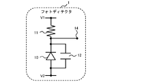
- FIG. 4 is a diagram showing a circuit example of the photodetector 1 according to the first embodiment.
- the photodetector 1 includes a SPAD 10, a first resistance 11 connected in series to the cathode of the SPAD 10, a first capacitance 12 connected in parallel to the SPAD 10, and an output unit 14 for outputting the cathode voltage of the SPAD 10.
- One end of the first resistor 11 is connected to the first power supply V1.
- the anode of SPAD10 is connected to the second power supply V2.
- the first capacitance 12 may be a parasitic capacitance of SPAD10, a capacitance element separate from the SPAD10, or both of them.
- the first capacitance 12 and the first resistor 11 may be formed by an LSI process or may be configured by an external circuit element. Both ends of the first capacitance 12 need not be connected to both ends of the SPAD 10, and only one end may be connected. At this time, it is the capacitance connected to the connected end of the first resistor 11 and the SPAD 10 that contributes to the capacitance C of the equation (21), and in FIG. 4, the first capacitance 12 connected to the cathode of the SPAD 10 Is.
- FIG. 5 is a diagram showing a modified example of the photodetector 1 according to the first embodiment.
- the photodetector 1 of FIG. 5 has a point that the first resistance 11 is a channel resistance of the first transistor 15 which is a transistor of a P-type channel and a point which includes a first variable power supply 16 with respect to the configuration of FIG. It's different.
- the differences will be mainly described.
- the first variable power supply 16 supplies a variable voltage as the gate voltage of the first transistor 15. At this time, the channel resistance of the first transistor 15 due to the gate voltage is set so as to satisfy the requirement of quenching resistance, that is, the equation (21).
- the first transistor 15 is connected to the cathode of the SPAD 10, but the conductive type is not limited, and for example, an N-type conductive transistor may be connected to the anode of the SPAD 10.
- Quenching requirements are determined by (i) the resistance value of the quenching resistor, (ii) the capacitance C of the SPAD10, (iii) the excess bias voltage Vex, (iv) the depletion layer width W, and (v) the breakdown voltage VBD .
- the above (i) to (v) are set so as to be determined and satisfy the equation (21).
- FIG. 6 is an example of a diagram showing whether or not quenching is possible with respect to the excess bias voltage Vex and the resistance value R of the first resistor 11.
- the dotted line is the calculation result of the formula (21), and the conditions of FIG. 1C were used except for Vex and R. Quenching can occur in the area to the upper right of the dotted line. However, quenching cannot occur in the lower left region, and the SPAD10 continues to multiply the avalanche.
- FIG. 7 is an example of a diagram showing whether or not quenching is possible with respect to the capacitance value C of the first capacitance 12 and the resistance value R of the first resistor 11.
- the dotted line is the calculation result of the equation (21), and the conditions of FIG. 1C were used except for C and R. Quenching can occur in the area to the upper right of the dotted line. However, quenching cannot occur in the lower left region, and the SPAD10 continues to multiply the avalanche.
- FIGS. 6 and 7 the correspondence between the circuit constants required for quenching and the device structure is illustrated.
- the SPAD 10 and the quenching circuit having a short dead time can be realized.
- the photodetector 1 includes a SPAD 10 and a first resistance 11 connected in series with the SPAD 10, and a recharge time during which electric charges are discharged from the SPAD 10 via the first resistance 11. In, the charge disappears from the multiplication region of SPAD10.
- the excess bias voltage applied to the SPAD 10 is smaller than the breakdown voltage of the SPAD 10, and the resistance value R of the first resistor 11 may satisfy the above equation (21).
- EBD in the equation (21) is the electric field strength inside the SPAD10
- C is the capacitance including the parasitic capacitance of the SPAD10
- Vex is the surplus bias voltage, which is the reverse bias voltage applied to the SPAD10 and the breakdown.
- W is the depleted layer width of SPAD10
- ⁇ (EBD) is the impact ionization rate of electrons under the electric field strength EBD
- ⁇ ( EBD ) is the electric field strength EBD .
- the impact ionization rate of holes a is the coefficient of impact ionization rate of electrons
- b is the coefficient of impact ionization rate of holes
- q is the elementary charge
- v s, e are. Indicates the electron saturation rate.
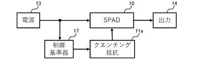
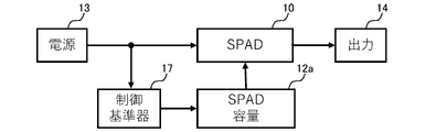
- FIG. 8 is a block diagram showing a configuration example of a control system including the photodetector 1 according to the second embodiment.
- This control system includes a power supply 13, a SPAD 10, a quenching resistance 11a, a control reference device 17, and an output unit 14.
- the SPAD 10 and the quenching resistor 11a correspond to the photodetector 1 in FIG.
- the quenching resistance 11a corresponds to the first transistor 15 and the first variable power supply 16 in FIG.
- the first variable power supply 16 outputs a variable voltage to the gate of the first transistor 15 according to the control of the control reference device 17.
- the control reference device 17 refers to the voltage of the power supply 13 and controls the resistance value R of the quenching resistor according to the relational expression of the equation (21).
- the control reference device 17 is configured by a CPU (Central Processing Unit) or the like, and Vex is calculated from the difference between the breakdown voltage recorded in advance and the power supply voltage.
- the gate voltage of the first transistor 15 is controlled according to the calculated Vex.
- the gate voltage may be controlled so that the channel resistance of the first transistor 15 is substantially inversely proportional to Vex. As a result, the resistance value R of the quenching resistor 11a can be reduced and the dead time can be further shortened even for different reverse bias voltages.
- the reverse bias voltage may be controlled according to the amount of incident light. For example, by setting Vex low under the condition that the amount of incident light is large and Vex high under the condition that the amount of incident light is small, the photodetector 1 having a wide dynamic range can be realized. At this time, by using the control system according to the second embodiment, the dead time can be further shortened and the dynamic range can be further expanded.
- FIG. 9 is a block diagram showing another configuration example of the control system including the photodetector 1 according to the second embodiment.
- the control target of the control reference device 17 is changed from the quenching resistance 11a to the SPAD capacity 12a as compared with the configuration of FIG.
- the control reference device 17 in FIG. 9 reduces the SPAD capacity 12a when the reverse bias voltage of the SPAD 10 is large, and increases the SPAD capacity 12a when the reverse bias voltage of the SPAD 10 is small. This can reduce the dead time for different reverse bias voltage values.
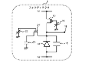
- FIG. 10 is a circuit diagram of a photodetector 1 that realizes the control system of FIG. 8 or FIG. FIG. 10 is different from the configuration of FIG. 5 in that the second transistor 21, the second variable power supply 22, and the second capacitance 23 are added. The differences will be mainly described below.
- the second transistor 21, which is an N-type transistor, is connected to the cathode of the SPAD 10.
- a second capacitance 23 is connected to the opposite end of the second transistor 21.
- the second variable power supply 22 is connected to the gate of the second transistor 21.
- the photodetector 1 of FIG. 10 When the photodetector 1 of FIG. 10 is included in the control system of FIG. 8, when the reverse bias voltage of the SPAD 10 is large, the gate voltage of the first transistor 15 is lowered to lower the channel resistance and the reverse bias voltage of the SPAD 10. When is small, the channel resistance is increased by increasing the gate voltage of the first transistor 15.
- the photodetector 1 of FIG. 10 When the photodetector 1 of FIG. 10 is included in the control system of FIG. 9, when the reverse bias voltage of the SPAD 10 is large, the second transistor 21 is put into a non-conducting state to reduce the size of the SPAD 10 and reverse the SPAD 10. When the bias voltage is small, the capacitance of the SPAD 10 is increased by making the second transistor 21 in a conductive state. This allows the dead time to be minimized for different Vex values. Both the quenching resistance 11a and the SPAD capacity 12a may be controlled at the same time.
- the parameters (i) to (v) may be controlled with respect to the temperature. Since the channel resistance of the first transistor 15 changes in temperature, the gate voltage may be controlled according to the temperature. In particular, if the excess bias voltage Vex is the same, the dead time is the same, so it is preferable to control the gate voltage so that the channel resistance of the first transistor 15 does not change in temperature. As a result, the dead time can be shortened even for different temperatures.
- the photodetector 1 includes a control reference device 17, and the control reference device 17 has the following five parameters (i) resistance value R of the first resistance 11 and (ii) SPAD10. Refer to any one or more of the capacitance C including the parasitic capacitance, (iii) the excess bias voltage Vex, (iv) the depleted layer width W of the SPAD10, and (v) the breakdown voltage, and set one or more parameters other than the referenced parameters. Control.
- the first resistance 11 is a variable resistance
- the control reference device 17 may reduce the resistance value of the first resistance 11 as the excess bias voltage increases.
- the first resistor 11 includes the first transistor 15, and the resistance value of the first resistor 11 may correspond to the channel resistance of the first transistor 15.
- the capacitance C including the parasitic capacitance of the SPAD 10 is variable, and the control reference device 17 may reduce the capacitance value of the capacitance C as the excess bias voltage increases.
- the second transistor 21 is provided at the connected end of the SPAD 10 and the first transistor 15, and the second capacitance is provided at the end opposite to the connected end of the second transistor 21, and the excess bias voltage of the SPAD 10 is applied.
- the gate voltage of the second transistor 21 may be controlled.
- FIG. 11 is a diagram showing a circuit example of the photodetector array according to the third embodiment.
- This photodetector array includes N photodetectors 1 (N is a natural number of 2 or more) in parallel, and further includes a second resistor 24.
- Each of the N photodetectors 1 includes a SPAD 10, a first transistor 15, and a first variable power supply 16.
- a second resistor 24 is connected between the SPAD 10 and the second power supply V2 at the end to which the photodetector 1 is connected, that is, the end to which the SPAD 10 is connected.
- the second resistor 24 is required to discharge the electric charge generated in all N SPAD 10s in a shorter time than the recharge time of the SPAD 10. That is, it is required that the time constant rNC due to the resistance value r of the second resistor 24 is shorter than the recharge time RC of the SPAD 10 due to the resistance value R of the first resistor 11. That is, it is required to satisfy the following equation.
- the resistance value r of the second resistor 24 may follow the following equation.
- the quenching characteristics are not deteriorated.
- it can be used for applications such as an image sensor and a photon counter in which a plurality of photodetectors 1 are arranged in an array.
- each photodetector 1 may include the output unit 14, or the output unit may be shared by N photodetectors 1.
- the connection unit between the cathode of the SPAD 10 and the first transistor 15 may be used as an output node.
- the output unit is shared by N photodetectors 1, the connection portion between the anode of the SPAD 10 and the second resistor 24 may be used as the output unit.
- FIG. 12 is a diagram showing a circuit example of the solid-state image sensor 100 according to the third embodiment.
- the solid-state image sensor 100 of FIG. 12 includes a control reference device 42, a selection unit 41, a load unit 43, a signal processing unit 44, a signal output line, and an output unit 45.
- the photodetector 1 of FIG. 12 is different from the photodetector 1 of FIG. 11A in that a third power supply V3, a third transistor 33, and a fourth transistor 34 are added.
- the differences will be mainly described.
- the third transistor 33 is an amplification transistor that outputs a voltage corresponding to the amount of electric charge to the cathode of the SPAD 10. Specifically, the third transistor 33 constitutes a source follower together with the load (for example, a constant current source) of the load unit 43 when the fourth transistor 34 is on.
- the fourth transistor 34 is a switch transistor for selection that is turned on in response to a selection control signal from the selection unit 41.
- the control reference device 42, the selection unit 41, and the signal processing unit 44 may be formed on a semiconductor substrate, and these may be collectively referred to as a peripheral circuit unit.
- the cathode of the SPAD 10 is connected to the gate of the third transistor 33, and the amount of current changes according to the cathode voltage of the SPAD 10.
- the selection unit 41 is connected to the gate of the fourth transistor 34 and selects at least one photodetector 1 that outputs a signal.
- the signal from the selected photodetector 1 is output to the signal processing unit 44 via the signal output line.
- the signal processed by the signal processing unit 44 is output from the output unit 45 as numerical data or image data.
- the output unit 45 is, for example, a display.
- the output from the photodetector 1 can be output in a format such as an image format.
- the conductive type of the third transistor 33 and the fourth transistor 34 is P-type, but may be N-type.
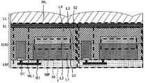
- FIG. 13 to 15 show the device structure of the photodetector array and the solid-state image sensor of the third embodiment.
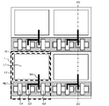
- FIG. 13 is a diagram showing a layout example of the solid-state image sensor 100 of FIG. 12 in a plan view.
- FIG. 13 shows a structure for 2 ⁇ 2 pixels.
- FIG. 13 shows a plurality of photodetectors 1, a SPAD10 in the photodetector 1, a first well WL1, a first wiring W1, a gate G1 of the first transistor 15, a gate G3 of the third transistor 33, and a fourth transistor.
- the gate G4 of 34, the 1-conductivity type first semiconductor layer L1 included in the SPAD10, and the 2nd conductive type third semiconductor layer L3 are provided.
- wirings other than the first wiring W1 and semiconductor layers other than the first semiconductor layer L1, the third semiconductor layer L3, and the first well WL1 are omitted.
- the first transistor 15, the third transistor 33, and the fourth transistor 34 are arranged in the first well WL1.
- the first semiconductor layer L1 is connected to the drain of the first transistor 15 and the gate G3 of the third transistor 33 by the first wiring W1.
- the source of the first transistor 15 is connected to the first power supply V1.
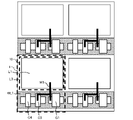
- FIG. 14 is a diagram showing a modified example of the layout of the solid-state image sensor 100 of the third embodiment in a plan view.
- the area of the gate G1 of the first transistor 15 is larger than that of the gate G3 of the third transistor 33 and the gate G4 of the fourth transistor 34 as compared with the layout of FIG.
- the area of the gate G1 of the first transistor 15 is larger than the gate area of the other transistors, that is, the third transistor 33 and the fourth transistor 34.
- the variation in the threshold voltage of the first transistor 15 can be suppressed, and the variation in the resistance of the first transistor 15 channel can be suppressed.
- the number of photodetectors 1 arranged in an array can be increased while satisfying the condition of the equation (21), and the dynamic range becomes wide.
- FIG. 15 is a diagram showing a cross-sectional configuration example of the solid-state image sensor 100 in the XV-XV line of FIG.
- the semiconductor substrate SUB, the wiring layer LM arranged so as to be in contact with the first main surface S1 side of the semiconductor substrate SUB, the electrode EL arranged so as to be in contact with the second main surface S2 side, and the upper part of the wiring layer LM were in contact with each other.
- the lens layer LL is provided, and the light irradiation surface is on the first main surface S1 side.
- a second conductive type second semiconductor layer L2 and a second conductive type fourth semiconductor layer L4 are provided in the semiconductor substrate SUB.
- the SPAD10 is composed of the first semiconductor layer L1, the second semiconductor layer L2, the third semiconductor layer L3, and the fourth semiconductor layer L4, and the periphery of the boundary between the first semiconductor layer L1 and the second semiconductor layer L2 is a multiplying region MP. be.
- the second semiconductor layers L2 are connected to each other through the semiconductor substrate SUB or the fourth semiconductor layer L4.
- the wiring layer LM omits parts other than the first wiring W1.
- the lens layer LL includes a microlens ML.
- the voltage application to the anode of the SPAD 10 that is, the voltage application to the second semiconductor layer L2 may be performed via the electrode EL.
- the second resistor 24 includes the junction between the semiconductor substrate SUB and the electrode EL, it is preferable that the resistance of the junction between the semiconductor substrate SUB and the electrode EL is low.
- the semiconductor substrate SUB is a type silicon, Ag, Pt, Ti, Au or the like may be used as the electrode material. As a result, the second resistance 24 can be lowered and the dynamic range can be expanded.
- the third semiconductor layer L3 has a function of separating between the first semiconductor layer L1 and the first semiconductor layer L1 and separating between the first semiconductor layer L1 and the first well WL1. At least a part of the region in contact with the first main surface S1 of the third semiconductor layer L3 may be depleted. As a result, the separation between the first semiconductor layer L1 and the first semiconductor layer L1 or between the first semiconductor layer L1 and the first well WL1 can be narrowed, and the photodetector 1 can be further miniaturized. Further, it is not necessary to arrange a contact or a trench in the region in contact with the first main surface S1 in the region where the third semiconductor layer L3 is arranged. As a result, defects in the third semiconductor layer L3 can be reduced, and dark current can be reduced.
- the second semiconductor layer L2, the third semiconductor layer L3, and the fourth semiconductor layer L4 are represented by different semiconductor layers for convenience, but they do not necessarily have to be formed by different impurity concentrations, different impurity injections, and the like. However, for example, the same impurity concentration may be used.
- FIG. 16 is a diagram showing a modified example of the cross-sectional configuration of the solid-state image sensor 100 in the XV-XV line of FIG.
- the light irradiation surface is changed from the first main surface S1 to the second main surface S2 side as compared with the configuration of FIG.
- the lens layer LL is arranged so as to be in contact with the upper part of the electrode EL. This can prevent light reflection in the wiring and improve the sensitivity.
- the electrode EL may be made of a material having high light transmittance. For example, when the wavelength range to be used is visible to near infrared, ITO (Indium Tin Oxide) or the like may be used.
- ITO Indium Tin Oxide
- FIG. 17 is a diagram showing another cross-sectional configuration example of the solid-state image sensor 100 according to the third embodiment.
- the figure shows a wider cross-sectional view as compared with FIG. It includes a light receiving region 46 provided with a plurality of photo detectors 1 and a contact region 47 outside the light receiving region 46.
- the contact region 47 includes a filter FL, a second wiring W2, and a fifth semiconductor layer L5.
- a voltage is applied to the anode of the SPAD 10 via the second wiring W2, the fifth semiconductor layer L5, the fourth semiconductor layer L4, and the electrode EL.
- a filter FL is provided in a region of the contact region 47 in contact with the second main surface S2 to prevent incident light from transmitting, whereby false detection caused by light incident on the contact region 47 is detected.
- the second resistor 24 is composed of the second wiring W2, the fifth semiconductor layer L5, the fourth semiconductor layer L4, and the electrode EL.
- the electrode EL does not necessarily have to be provided.
- the fourth semiconductor layer L4 and the fifth semiconductor layer L5 may have an increased impurity concentration in order to reduce the diffusion resistance, whereby the formula (23) or the formula (24), which is a requirement of the second resistance 24, may be increased. ) Will be easier to satisfy.
- the impurity concentration may be gradually increased from the first main surface S1 side to the second main surface S2 side.
- the electric charge generated in the fourth semiconductor layer L4 is transferred to the multiplying region MP by the built-in potential of the fourth semiconductor layer L4, and the sensitivity can be improved.
- the configuration is such that light is emitted from the second main surface S2 in FIG. 17, the configuration may be such that light is emitted from the first main surface S1.
- FIG. 18 is a schematic layout diagram of the solid-state image sensor 100 of FIG. 17 as a whole in a plan view.
- FIG. 18 includes a chip, a light receiving region 46, a contact region 47, a control reference device 42, a selection unit 41, and a signal processing unit 44 in the chip.
- the contact region 47 is arranged adjacent to the light receiving region 46 and is arranged so as to surround the periphery of the light receiving region 46.
- the control reference device 42, the selection unit 41, and the signal processing unit 44 are arranged on the outer periphery of the contact area 47.
- the second resistance 24 can be further reduced, and a photodetector array with a wide dynamic range can be realized.
- the contact region 47 is arranged outside the control reference device 42, the selection unit 41, or the signal processing unit 44. Is also good.
- the photodetector array according to the third embodiment includes N of the above photodetectors 1 (N is an integer of 2 or more), and the N series circuits included in the N photodetectors 1 are arranged in parallel.
- Each of the N series circuits connected has a SPAD10 and a first resistance 11 connected in series, and one end of the N series circuit and the N ends on the SPAD10 side are connected to each other, and further.
- a second resistance 24 connected to one end of N connected to each other and connected in series with the N photodetectors is provided, and the resistance value of the second resistance 24 is the N component of the resistance value of the first resistance 11. Less than 1 of.
- N SPAD10s may be arranged on the same semiconductor substrate, and one end of N connected to each other may be connected via the semiconductor substrate.
- an electrode arranged in contact with the second main surface which is the main surface of the semiconductor substrate and which is the main surface on the side of one end of the N pieces connected to each other.
- a voltage may be applied to one end of the N pieces connected to each other via an electrode arranged in contact with the second main surface which is the main surface of the semiconductor substrate and which is the main surface on the side of one end of the N pieces connected to each other.
- the light receiving region in which N photodetectors are arranged the contact region arranged outside the light receiving region, and the contact region so as to be in contact with the first main surface which is the main surface opposite to the second main surface.
- a second wiring is provided, and a voltage may be applied to one end of the N pieces connected to each other via the second wiring.
- a peripheral circuit unit that controls N photodetectors or performs signal processing may be provided, and the contact region may be arranged between the light receiving region and the peripheral circuit unit.
- each of the N photodetectors includes at least two transistors including the first transistor, the first resistor 11 is the channel resistance of the first transistor 15, and the gate area of the first transistor 15 is the other that the photodetector has. It may be larger than the gate area of the transistor of.
- the photodetector array according to the third embodiment includes M of the above photodetectors 1 (M is an integer of 2 or more), and the photodetectors 1 are connected to each other at one end of the SPAD 10 and a third is connected to the connected ends.
- the resistance 31 and the third capacitance 32 are connected, the first resistance 11 is the first transistor 15, and the resistance value r'of the third resistance 31 satisfies the equation (25).
- the first transistor 15 may be in a conductive state during the reset period for resetting the SPAD 10, and may be in the non-conducting state during the exposure period for detecting the light incident on the SPAD 10.
- the conductive type of the channel of the first transistor 15 may be the same as the conductive type of the end to which the first transistor 15 is connected in SPAD10.
- the capacity value of the third capacity may be larger than the capacity of SPAD10.
- FIG. 19 is an application example of a photodetector or a photodetector array, and is a block diagram showing an example of a distance measurement system using the photodetector 1 or the photodetector array according to the present disclosure.
- the distance measurement system 500 has a light emitting unit 510 that emits pulsed light, a light receiving unit 520 that receives reflected pulsed light, and a control unit that controls the light emitting unit 510 and the light receiving unit 520. It has a 530 and an output unit 540 that outputs a signal from the light receiving unit 520.
- the light emitting unit 510 is composed of a light emitting device such as a light emitting diode, generates pulsed light by a control signal from the control unit 530, and irradiates the measurement object 600.
- the light emitting unit 510 may be a diffusion light source, and the measurement object 600 may be a plurality.
- the light receiving unit 520 is the photodetector 1, the photodetector array, or the solid-state image pickup device 100 according to the above-described embodiment, and receives the pulsed light reflected by the measurement object 600.
- the light receiving unit 520 may be provided with an optical system such as a lens, and may be imaged on the photodetector 1 or the photodetector array surface.
- the control unit 530 is composed of a CPU (Central Processing Unit) or the like, and controls both of the light emitting unit 510 and the light receiving unit 520 so as to operate in synchronization with each other. Further, the control unit 530 measures the time until the pulsed light is reflected from the measurement object 600 and returns to the light receiving unit 520 based on the control signal to the light emitting unit 510 and the output signal from the light receiving unit 520. Thereby, the distance to the measurement object 600 is calculated.
- CPU Central Processing Unit
- the output unit 540 outputs the distance to the measurement object 600 calculated by the control unit 530 in a numerical data format or an image format.
- the output unit 540 is usually composed of a display, for example, a liquid crystal display, an organic EL display, or the like.
- the distance measurement system 500 is a so-called TOF (Time Of Flite) type distance measurement system.
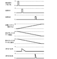
- FIG. 20 is a diagram showing an example of a timing chart in the distance measurement measurement system 500 of FIG.
- the timing chart shows the pulsed light of the light emitting unit, the reflected light 1, the reflected light 2, the excess bias voltage Vex, the gate voltage of the first transistor 15, the channel resistance of the first transistor 15, the SPAD1 output, and the SPAD2.
- the vertical axis includes the output, the pulsed light of the light emitting part, the reflected light 1, and the reflected light 2 represent the light intensity, the surplus bias voltage, the gate voltage of the first transistor 15, the SPAD1 output, and the SPAD2 output. Represents the voltage, and the channel resistance of the first transistor 15 represents the resistance value.
- the horizontal axis shows time.
- SPAD1 and SPAD2 are one of SPAD10 in the photodetector array, and their positions are not limited.
- the light emitting unit is a diffusion light source, and there are at least two or more objects to be measured, and there are a relatively close object to be measured and a relatively distant object to be measured.
- the reflected light 1 is light that is irradiated to a relatively close object to be measured and is reflected and then incident on SPAD1
- the reflected light 2 is irradiated to a relatively nearby object to be measured and is reflected and then incident on SPAD2. It is light.
- Vex is increased with time.
- the light intensity decreases in inverse proportion to the square of the distance, so that the reflected light from a nearby object to be measured has a high light intensity.
- the light intensity of the reflected light from a distant object to be measured is low. Therefore, when detecting reflected light from a nearby object to be measured, Vex is lowered and the light detection efficiency (Photon Detection Efficiency (PDE)) is lowered to prevent double counting and erroneous due to dark current.
- PDE Photon Detection Efficiency
- the detection probability can be reduced.
- the resistance value may be lowered with time in order to realize quenching while minimizing the dead time. For example, in the circuit of FIG. 12A, since the quenching resistance is a P-type transistor, the gate voltage may be lowered with time.
- the distance measuring measurement system 500 controls the light receiving unit 520 having the photodetector 1, the light emitting unit 510 that emits light toward the object to be measured, and the light receiving unit 520 and the light emitting unit 510.
- the control unit 530 receives a signal corresponding to the reflected light reflected by the measurement object from the light receiving unit 510, and calculates the distance to the measurement object.
- the excess bias voltage may be increased with time, and the channel resistance of the first transistor 15 may be lowered with time.
- the present disclosure is not limited to this embodiment. As long as it does not deviate from the gist of the present disclosure, various modifications that can be conceived by those skilled in the art are applied to this embodiment, and a form constructed by combining components in different embodiments is also within the scope of one or more embodiments. May be included within.
- the present disclosure can be used for a photodetector, a photodetector array, a distance measuring system, and for example, a solid-state image sensor, a distance measuring device, a camera, and the like.
Landscapes
- Engineering & Computer Science (AREA)
- Physics & Mathematics (AREA)
- Computer Networks & Wireless Communication (AREA)
- General Physics & Mathematics (AREA)
- Radar, Positioning & Navigation (AREA)
- Remote Sensing (AREA)
- Electromagnetism (AREA)
- Light Receiving Elements (AREA)
Priority Applications (3)
| Application Number | Priority Date | Filing Date | Title |
|---|---|---|---|
| CN202180081353.7A CN116547821A (zh) | 2020-12-10 | 2021-11-15 | 光电检测器、光电检测器阵列及距离测量系统 |
| JP2022568139A JP7745207B2 (ja) | 2020-12-10 | 2021-11-15 | フォトディテクタ、フォトディテクタアレイおよび距離測定システム |
| US18/325,709 US20230299114A1 (en) | 2020-12-10 | 2023-05-30 | Photodetector, photodetector array, and distance measurement system |
Applications Claiming Priority (2)
| Application Number | Priority Date | Filing Date | Title |
|---|---|---|---|
| JP2020205037 | 2020-12-10 | ||
| JP2020-205037 | 2020-12-10 |
Related Child Applications (1)
| Application Number | Title | Priority Date | Filing Date |
|---|---|---|---|
| US18/325,709 Continuation US20230299114A1 (en) | 2020-12-10 | 2023-05-30 | Photodetector, photodetector array, and distance measurement system |
Publications (1)
| Publication Number | Publication Date |
|---|---|
| WO2022124019A1 true WO2022124019A1 (ja) | 2022-06-16 |
Family
ID=81972961
Family Applications (1)
| Application Number | Title | Priority Date | Filing Date |
|---|---|---|---|
| PCT/JP2021/041947 Ceased WO2022124019A1 (ja) | 2020-12-10 | 2021-11-15 | フォトディテクタ、フォトディテクタアレイおよび距離測定システム |
Country Status (4)
| Country | Link |
|---|---|
| US (1) | US20230299114A1 (https=) |
| JP (1) | JP7745207B2 (https=) |
| CN (1) | CN116547821A (https=) |
| WO (1) | WO2022124019A1 (https=) |
Cited By (1)
| Publication number | Priority date | Publication date | Assignee | Title |
|---|---|---|---|---|
| WO2024176708A1 (ja) * | 2023-02-20 | 2024-08-29 | ソニーセミコンダクタソリューションズ株式会社 | 光検出装置 |
Families Citing this family (3)
| Publication number | Priority date | Publication date | Assignee | Title |
|---|---|---|---|---|
| JP7614855B2 (ja) * | 2021-01-22 | 2025-01-16 | キヤノン株式会社 | 光電変換装置、光検出システム |
| EP4254017A1 (en) * | 2022-03-28 | 2023-10-04 | Koninklijke Philips N.V. | Photon counting detector and photon counting method |
| WO2025155931A1 (en) * | 2024-01-17 | 2025-07-24 | Government Of The United States Of America, As Represented By The Secretary Of Commerce | Metrological photon counter and metrologically counting photons at room temperature |
Citations (4)
| Publication number | Priority date | Publication date | Assignee | Title |
|---|---|---|---|---|
| JP2018179732A (ja) * | 2017-04-12 | 2018-11-15 | 株式会社デンソー | 光検出器 |
| US10312274B1 (en) * | 2018-01-29 | 2019-06-04 | Stmicroelectronics (Research & Development) Limited | Single photon avalanche diode (SPAD) with variable quench resistor |
| JP2019190892A (ja) * | 2018-04-20 | 2019-10-31 | ソニーセミコンダクタソリューションズ株式会社 | 受光装置及び測距装置 |
| WO2020179696A1 (ja) * | 2019-03-07 | 2020-09-10 | ソニーセミコンダクタソリューションズ株式会社 | 受光装置および測距装置 |
-
2021
- 2021-11-15 CN CN202180081353.7A patent/CN116547821A/zh active Pending
- 2021-11-15 JP JP2022568139A patent/JP7745207B2/ja active Active
- 2021-11-15 WO PCT/JP2021/041947 patent/WO2022124019A1/ja not_active Ceased
-
2023
- 2023-05-30 US US18/325,709 patent/US20230299114A1/en active Pending
Patent Citations (4)
| Publication number | Priority date | Publication date | Assignee | Title |
|---|---|---|---|---|
| JP2018179732A (ja) * | 2017-04-12 | 2018-11-15 | 株式会社デンソー | 光検出器 |
| US10312274B1 (en) * | 2018-01-29 | 2019-06-04 | Stmicroelectronics (Research & Development) Limited | Single photon avalanche diode (SPAD) with variable quench resistor |
| JP2019190892A (ja) * | 2018-04-20 | 2019-10-31 | ソニーセミコンダクタソリューションズ株式会社 | 受光装置及び測距装置 |
| WO2020179696A1 (ja) * | 2019-03-07 | 2020-09-10 | ソニーセミコンダクタソリューションズ株式会社 | 受光装置および測距装置 |
Cited By (1)
| Publication number | Priority date | Publication date | Assignee | Title |
|---|---|---|---|---|
| WO2024176708A1 (ja) * | 2023-02-20 | 2024-08-29 | ソニーセミコンダクタソリューションズ株式会社 | 光検出装置 |
Also Published As
| Publication number | Publication date |
|---|---|
| CN116547821A (zh) | 2023-08-04 |
| US20230299114A1 (en) | 2023-09-21 |
| JP7745207B2 (ja) | 2025-09-29 |
| JPWO2022124019A1 (https=) | 2022-06-16 |
Similar Documents
| Publication | Publication Date | Title |
|---|---|---|
| JP7745207B2 (ja) | フォトディテクタ、フォトディテクタアレイおよび距離測定システム | |
| US11791433B2 (en) | Single photon avalanche diode | |
| JP7145454B2 (ja) | フォトセンサ、イメージセンサ及びフォトセンサの駆動方法 | |
| CN106449669A (zh) | 光电转换器件、测距装置和信息处理系统 | |
| US12080729B2 (en) | Photodetector | |
| US12317614B2 (en) | Semiconductor device and electronic apparatus including PN junction portions | |
| US20220246782A1 (en) | Photo sensor and distance measuring system using said photo sensor | |
| JP2019169643A (ja) | 固体撮像素子 | |
| JPWO2022124019A5 (https=) | ||
| US20230358534A1 (en) | Photodetector and distance measuring system | |
| JP7570037B2 (ja) | フォトセンサ及び距離測定システム | |
| JP2018006989A (ja) | 光学装置およびシステム | |
| WO2022070655A1 (ja) | フォトディテクタ、フォトディテクタアレイおよび駆動方法 | |
| JP2017036971A (ja) | 光電変換デバイス、測距装置および情報処理システム | |
| US20170160406A1 (en) | Photodetector, and ct device including said photodetector | |
| US20250151429A1 (en) | Single photon avalanche diode | |
| US20230035346A1 (en) | Light detection device and method for driving photosensor | |
| Isaak et al. | Design and characterisation of 16× 1 parallel outputs SPAD array in 0.18 um CMOS technology | |
| JP2017037937A (ja) | 光電変換デバイス、測距装置および情報処理システム | |
| US20260123075A1 (en) | Semiconductor device with optical structure for enhancing blue light detection | |
| JP6700687B2 (ja) | 光電変換デバイス、測距装置および情報処理システム | |
| JPWO2019180898A1 (ja) | 固体撮像素子 | |
| CN107408564A (zh) | 具有对数响应和扩展的温度操作范围的矩阵传感器 | |
| CN120417510A (zh) | 单光子雪崩二极管及包括其的图像感测装置 | |
| JP2020129673A (ja) | 光検出装置およびこれを用いた被写体検知システム |
Legal Events
| Date | Code | Title | Description |
|---|---|---|---|
| 121 | Ep: the epo has been informed by wipo that ep was designated in this application |
Ref document number: 21903123 Country of ref document: EP Kind code of ref document: A1 |
|
| ENP | Entry into the national phase |
Ref document number: 2022568139 Country of ref document: JP Kind code of ref document: A |
|
| WWE | Wipo information: entry into national phase |
Ref document number: 202180081353.7 Country of ref document: CN |
|
| NENP | Non-entry into the national phase |
Ref country code: DE |
|
| 122 | Ep: pct application non-entry in european phase |
Ref document number: 21903123 Country of ref document: EP Kind code of ref document: A1 |