WO2022123379A1 - 表示装置、表示装置の作製方法、及び電子機器 - Google Patents
表示装置、表示装置の作製方法、及び電子機器 Download PDFInfo
- Publication number
- WO2022123379A1 WO2022123379A1 PCT/IB2021/060903 IB2021060903W WO2022123379A1 WO 2022123379 A1 WO2022123379 A1 WO 2022123379A1 IB 2021060903 W IB2021060903 W IB 2021060903W WO 2022123379 A1 WO2022123379 A1 WO 2022123379A1
- Authority
- WO
- WIPO (PCT)
- Prior art keywords
- layer
- light emitting
- lens
- display device
- conductive layer
- Prior art date
- Legal status (The legal status is an assumption and is not a legal conclusion. Google has not performed a legal analysis and makes no representation as to the accuracy of the status listed.)
- Ceased
Links
Images


Classifications
-
- H—ELECTRICITY
- H10—SEMICONDUCTOR DEVICES; ELECTRIC SOLID-STATE DEVICES NOT OTHERWISE PROVIDED FOR
- H10K—ORGANIC ELECTRIC SOLID-STATE DEVICES
- H10K59/00—Integrated devices, or assemblies of multiple devices, comprising at least one organic light-emitting element covered by group H10K50/00
- H10K59/80—Constructional details
- H10K59/875—Arrangements for extracting light from the devices
- H10K59/879—Arrangements for extracting light from the devices comprising refractive means, e.g. lenses
-
- G—PHYSICS
- G09—EDUCATION; CRYPTOGRAPHY; DISPLAY; ADVERTISING; SEALS
- G09F—DISPLAYING; ADVERTISING; SIGNS; LABELS OR NAME-PLATES; SEALS
- G09F9/00—Indicating arrangements for variable information in which the information is built-up on a support by selection or combination of individual elements
- G09F9/30—Indicating arrangements for variable information in which the information is built-up on a support by selection or combination of individual elements in which the desired character or characters are formed by combining individual elements
-
- H—ELECTRICITY
- H05—ELECTRIC TECHNIQUES NOT OTHERWISE PROVIDED FOR
- H05B—ELECTRIC HEATING; ELECTRIC LIGHT SOURCES NOT OTHERWISE PROVIDED FOR; CIRCUIT ARRANGEMENTS FOR ELECTRIC LIGHT SOURCES, IN GENERAL
- H05B33/00—Electroluminescent light sources
- H05B33/02—Details
-
- H—ELECTRICITY
- H05—ELECTRIC TECHNIQUES NOT OTHERWISE PROVIDED FOR
- H05B—ELECTRIC HEATING; ELECTRIC LIGHT SOURCES NOT OTHERWISE PROVIDED FOR; CIRCUIT ARRANGEMENTS FOR ELECTRIC LIGHT SOURCES, IN GENERAL
- H05B33/00—Electroluminescent light sources
- H05B33/10—Apparatus or processes specially adapted to the manufacture of electroluminescent light sources
-
- H—ELECTRICITY
- H10—SEMICONDUCTOR DEVICES; ELECTRIC SOLID-STATE DEVICES NOT OTHERWISE PROVIDED FOR
- H10K—ORGANIC ELECTRIC SOLID-STATE DEVICES
- H10K59/00—Integrated devices, or assemblies of multiple devices, comprising at least one organic light-emitting element covered by group H10K50/00
- H10K59/10—OLED displays
- H10K59/12—Active-matrix OLED [AMOLED] displays
- H10K59/1201—Manufacture or treatment
-
- H—ELECTRICITY
- H10—SEMICONDUCTOR DEVICES; ELECTRIC SOLID-STATE DEVICES NOT OTHERWISE PROVIDED FOR
- H10K—ORGANIC ELECTRIC SOLID-STATE DEVICES
- H10K2102/00—Constructional details relating to the organic devices covered by this subclass
- H10K2102/301—Details of OLEDs
- H10K2102/302—Details of OLEDs of OLED structures
- H10K2102/3023—Direction of light emission
- H10K2102/3026—Top emission
-
- H—ELECTRICITY
- H10—SEMICONDUCTOR DEVICES; ELECTRIC SOLID-STATE DEVICES NOT OTHERWISE PROVIDED FOR
- H10K—ORGANIC ELECTRIC SOLID-STATE DEVICES
- H10K59/00—Integrated devices, or assemblies of multiple devices, comprising at least one organic light-emitting element covered by group H10K50/00
- H10K59/80—Constructional details
- H10K59/87—Passivation; Containers; Encapsulations
- H10K59/873—Encapsulations
Definitions
- One aspect of the present invention relates to a display device.
- One aspect of the present invention relates to a method for manufacturing a display device.
- One aspect of the present invention relates to an electronic device.
- one aspect of the present invention is not limited to the above technical fields.
- the technical fields of one aspect of the present invention disclosed in the present specification and the like include semiconductor devices, display devices, light emitting devices, power storage devices, storage devices, electronic devices, lighting devices, input devices, input / output devices, and driving methods thereof. , Or their manufacturing method, can be mentioned as an example.
- a semiconductor device refers to all devices that can function by utilizing semiconductor characteristics.
- examples of the display device applicable to the display panel include a light emitting device including an organic EL (Electroluminescence) element or a light emitting element such as a light emitting diode (LED: Light Emitting Diode).
- a light emitting device including an organic EL (Electroluminescence) element or a light emitting element such as a light emitting diode (LED: Light Emitting Diode).
- the basic configuration of an organic EL device is such that a layer containing a luminescent organic compound is sandwiched between a pair of electrodes. By applying a voltage to this device, light emission can be obtained from a luminescent organic compound. Since the display device to which such an organic EL element is applied does not require a backlight, which is required for a liquid crystal display device or the like, a thin, lightweight, high-contrast, and low-power consumption display device can be realized. For example, an example of a display device using an organic EL element is described in Patent Document 1.
- One aspect of the present invention is to provide a display device capable of displaying a high-quality image. Further, one aspect of the present invention is to provide a high-definition display device. Further, one aspect of the present invention is to provide a display device that can be manufactured by a simple method. Further, one aspect of the present invention is to provide a low-priced display device. Further, one aspect of the present invention is to provide a highly reliable display device. Further, one aspect of the present invention is to provide a new display device.
- Another object of the present invention is to provide a method for manufacturing a display device capable of displaying a high-quality image. Further, one aspect of the present invention is to provide a method for manufacturing a high-definition display device. Further, one aspect of the present invention is to provide a method for manufacturing a simple display device. Further, one aspect of the present invention is to provide a method for manufacturing a low-priced display device. Further, one aspect of the present invention is to provide a method for manufacturing a highly reliable display device. Further, one aspect of the present invention is to provide a method for manufacturing a new display device.
- One aspect of the present invention includes a first conductive layer, a second conductive layer, a light emitting layer, and a lens, and a light emitting layer is provided on the first conductive layer, and the light emitting layer is on the light emitting layer.
- a second conductive layer is provided, a lens is provided on the second conductive layer, the lens contains a photosensitive material, and the end of the lens is the end of the light emitting layer, and the second. It is a display device located outside the end of the conductive layer.
- the lens may contain an acrylic resin.
- the first insulating layer has a first insulating layer, and the first insulating layer has a region in contact with the upper surface of the lens, a region in contact with the side surface of the second conductive layer, and a region in contact with the side surface of the light emitting layer. You may.
- the second insulating layer is provided, the second insulating layer is provided between the second conductive layer and the lens, and the end portion of the second insulating layer is the lens. It may be located inside the end.
- one aspect of the present invention includes a first conductive layer, a second conductive layer, a third conductive layer, a fourth conductive layer, a first light emitting layer, and a second light emitting layer. It has a first lens, a second lens, a first colored layer, and a second colored layer, and a first light emitting layer is provided on the first conductive layer, and the first A second conductive layer is provided on the light emitting layer, a first lens is provided on the second conductive layer, a first colored layer is provided on the first lens, and a third A second light emitting layer is provided on the conductive layer, a fourth conductive layer is provided on the second light emitting layer, a second lens is provided on the fourth conductive layer, and a second lens is provided.
- a second colored layer is provided on the lens, the first lens and the second lens contain a photosensitive material, and the end of the first lens is the end of the first light emitting layer. , And the end of the second lens is located outside the end of the second conductive layer, and the end of the second lens is located outside the end of the second light emitting layer and the end of the fourth conductive layer.
- the first light emitting layer and the second light emitting layer have a function of emitting light of the same color, and the first colored layer and the second colored layer have a function of transmitting light of different colors. You may.
- the first lens and the second lens may contain an acrylic resin.
- the first insulating layer is provided, and the first insulating layer includes a region in contact with the upper surface of the first lens, a region in contact with the upper surface of the second lens, and a side surface of the second conductive layer. It may have a region in contact with the side surface of the fourth conductive layer, a region in contact with the first light emitting layer, and a region in contact with the side surface of the second light emitting layer.
- a second insulating layer and a third insulating layer are provided, and the second insulating layer is provided between the second conductive layer and the first lens.
- the third insulating layer is provided between the fourth conductive layer and the second lens, and the end portion of the second insulating layer is located inside the end portion of the first lens.
- the end of the insulating layer 3 may be located inside the end of the second lens.
- An electronic device having a display device and an operation button according to an aspect of the present invention is also an aspect of the present invention.
- a first conductive layer is formed on a substrate, a film to be a light emitting layer is formed on the first conductive layer, and a second film is formed on the film to be a light emitting layer.
- a film to be a conductive layer is formed, a resist mask is formed on the film to be a second conductive layer so as to have a region overlapping with the first conductive layer, a film to be a second conductive layer, and light emission.
- the first insulating layer may be formed after the lens is formed.
- the first insulating layer may be formed by the ALD method.
- the film to be the second insulating layer is formed, and after the resist mask is formed, the second insulation is formed.
- a second insulating layer, a second conductive layer, and a light emitting layer are formed by etching a film to be a layer, a film to be a second conductive layer, and a film to be a light emitting layer using a resist mask as a mask. You may.
- a display device capable of displaying a high-quality image.
- a high-definition display device can be provided.
- a display device that can be manufactured by a simple method.
- a low-priced display device can be provided.
- a highly reliable display device can be provided.
- a novel display device can be provided.
- a method for manufacturing a display device capable of displaying a high-quality image. Further, according to one aspect of the present invention, it is possible to provide a method for manufacturing a high-definition display device. Further, according to one aspect of the present invention, it is possible to provide a simple method for manufacturing a display device. Further, according to one aspect of the present invention, it is possible to provide a method for manufacturing a low-priced display device. Further, according to one aspect of the present invention, it is possible to provide a method for manufacturing a highly reliable display device. Further, according to one aspect of the present invention, it is possible to provide a method for manufacturing a novel display device.
- FIG. 1 is a cross-sectional view showing a configuration example of a display device.
- 2A to 2D are cross-sectional views showing an example of a method for manufacturing a display device.
- 3A to 3D are cross-sectional views showing an example of a method for manufacturing a display device.
- FIG. 4 is a cross-sectional view showing a configuration example of the display device.
- 5A and 5B are block diagrams showing a configuration example of a display device.
- 6A and 6B are perspective views showing a configuration example of the touch panel.
- 7A1 to 7C1 and FIGS. 7A2 to 7C2 are cross-sectional views showing a configuration example of a transistor. 8A1 to 8A3, FIGS.
- 8B1, 8B2, 8C1 and 8C2 are cross-sectional views showing a configuration example of a transistor.
- 9A to 9F are views showing a configuration example of an electronic device.
- 10A and 10B are diagrams showing a configuration example of a display module.
- 11A and 11B are diagrams showing a configuration example of an electronic device.
- 12A to 12E are diagrams showing a configuration example of an electronic device.
- 13A to 13G are diagrams showing a configuration example of an electronic device.
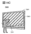
- 14A to 14D are diagrams showing a configuration example of an electronic device.
- a metal oxide is a metal oxide in a broad sense. Metal oxides are classified into oxide insulators, oxide conductors (including transparent oxide conductors), oxide semiconductors (also referred to as Oxide Semiconductor or simply OS) and the like. For example, when a metal oxide is used for the active layer of a transistor, the metal oxide may be referred to as an oxide semiconductor. That is, when a metal oxide can form a channel forming region of a transistor having at least one of an amplification action, a rectifying action, and a switching action, the metal oxide can be referred to as a metal oxide semiconductor. can. Further, in the case of describing as an OS FET or an OS transistor, it can be paraphrased as a transistor having a metal oxide or an oxide semiconductor.
- a device manufactured by using a metal mask or an FMM may be referred to as a device having an MM (metal mask) structure.
- a device manufactured without using a metal mask or FMM may be referred to as a device having an MML (metal maskless) structure.
- One aspect of the present invention relates to a display device having a light emitting element such as an organic EL element as a display element, and a method for manufacturing the same.
- a first conductive layer is formed on the first substrate.
- a film to be a light emitting layer is formed on the first conductive layer.
- a film to be a second conductive layer is formed on the film to be a light emitting layer.
- a resist mask is formed on the film to be the second conductive layer so as to have a region overlapping with the first conductive layer. Then, the film to be the second conductive layer and the film to be the light emitting layer are etched using the resist mask as a mask. As a result, an island-shaped second conductive layer and a light emitting layer are formed.
- the light emitting element has a configuration in which a light emitting layer is provided between the first conductive layer and the second conductive layer.
- the first conductive layer serves as one electrode of the light emitting element, and the second conductive layer serves as the other electrode of the light emitting element.
- the first substrate on which the light emitting element is formed is heated.
- the resist mask is deformed into a convex shape and has a function as a lens.
- an insulating layer is formed so as to have a region in contact with the side surface of the second conductive layer and the side surface of the light emitting layer.
- a colored layer is formed on the second substrate, and the colored layer and the insulating layer are bonded together by an adhesive layer.
- the light emitting layer can be separated between the pixels, and the electrode provided on the light emitting layer (the other electrode of the light emitting element) can be separated between the pixels.
- the display device according to one aspect of the present invention can be a high-definition display device.
- a second conductive layer and a light emitting layer are formed by etching using a resist mask as a mask, and then the resist mask is heated to form a lens. Therefore, for example, the manufacturing process can be simplified as compared with the case where the resist mask is removed to form the lens. From the above, the display device can be manufactured by a simple method by the above method, and thus the display device according to one aspect of the present invention can be made into a low-priced display device.
- the term “element” may be paraphrased as “device”.
- the light emitting element can be said to be a light emitting device.
- FIG. 1 is a cross-sectional view showing a configuration example of a display device 10 which is a display device of one aspect of the present invention.
- the display device 10 has a pixel 15R, a pixel 15G, and a pixel 15B.
- the pixels 15R, the pixels 15G, and the pixels 15B are provided on the display surface of the display device 10.
- the display surface can be configured such that the pixels 15R, the pixels 15G, and the pixels 15B are arranged in a matrix. It can be said that one pixel is composed of the pixel 15R, the pixel 15G, and the pixel 15B, and the pixels are arranged in a matrix on the display surface of the display device 10. In this case, it can be said that the pixel 15R, the pixel 15G, and the pixel 15B are sub-pixels, respectively.
- the display device 10 includes a substrate 11, a transistor 52, an insulating layer 13, a light emitting element 30, a partition wall 14, an insulating layer 63, a lens 29, an insulating layer 21, an adhesive layer 33, and a colored layer 25R. It has a colored layer 25G, a colored layer 25B, a light-shielding layer 45, and a substrate 12.
- the colored layer 25R, the colored layer 25G, and the colored layer 25B are collectively referred to as a colored layer 25.
- One light emitting element 30 and one lens 29 are provided for each of the pixel 15R, the pixel 15G, and the pixel 15B.
- the insulating layer 63 is provided separately for each pixel. Further, the colored layer 25R is provided on the pixel 15R, the colored layer 25G is provided on the pixel 15G, and the colored layer 25B is provided on the pixel 15B.
- the pixel 15G is adjacent to the pixel 15R and the pixel 15B.
- the light emitting elements 30 provided in the adjacent pixels, the colored layers, or the lenses 29 are adjacent to each other.
- the light emitting element 30 provided in the pixel 15R shown in FIG. 1 and the light emitting element 30 provided in the pixel 15G are adjacent to each other.
- the colored layer 25R and the colored layer 25G shown in FIG. 1 are adjacent to each other.
- the lens 29 provided in the pixel 15R shown in FIG. 1 and the lens 29 provided in the pixel 15G are adjacent to each other.
- the pixel 15R and the pixel 15B are not adjacent to each other in FIG. 1, the pixel 15R and the pixel 15B may be adjacent to each other.
- the insulating layer 13 and the transistor 52 are provided on the substrate 11.
- the light emitting element 30 is provided on the insulating layer 13.
- the insulating layer 63 is provided on the light emitting element 30.
- the lens 29 is provided on the insulating layer 63.
- the insulating layer 21 is provided on the lens 29 and the partition wall 14.
- the adhesive layer 33 is provided on the insulating layer 21.
- the colored layer 25R, the colored layer 25G, the colored layer 25B, and the light-shielding layer 45 are provided on the adhesive layer 33.
- the substrate 12 is provided on the colored layer 25R, the colored layer 25G, the colored layer 25B, and the light-shielding layer 45.
- an insulating substrate such as a glass substrate, a quartz substrate, a sapphire substrate, a ceramic substrate, a single crystal semiconductor substrate made of silicon or silicon carbide, a polycrystalline semiconductor substrate, a compound semiconductor substrate such as silicon germanium, etc.
- a semiconductor substrate such as an SOI substrate can be used.
- the substrate 12 for example, a substrate having transparency to visible light is used.
- a glass substrate, a quartz substrate, a sapphire substrate, or the like can be used.
- the display device 10 can be made into a flexible display device.
- an organic insulating film as the insulating layer 13.
- the organic insulating film include acrylic resin, polyimide resin, epoxy resin, polyamide resin, polyimideamide resin, siloxane resin, benzocyclobutene resin, phenol resin, and precursors of these resins.
- an inorganic insulating film as the insulating layer 63 and the insulating layer 21.
- an aluminum oxide film, an aluminum nitride film, a silicon nitride film, a silicon nitride film, a silicon oxide film, a silicon nitride film, or the like can be used.
- two or more of the above-mentioned insulating films may be laminated and used.
- An inorganic insulating film may be used as the insulating layer 13, or an organic insulating film may be used as the insulating layer 63 and the insulating layer 21.
- the same material as the material that can be used as the insulating layer 13, the insulating layer 63, or the insulating layer 21 can be used.
- silicon oxide has a higher oxygen content than nitrogen as its composition. Further, the silicon nitride oxide indicates a composition having a nitrogen content higher than that of oxygen.
- the colored layer 25R, the colored layer 25G, and the colored layer 25B are provided on different light emitting elements 30 and lenses 29, respectively. Therefore, the light emitting element 30, the lens 29, and the colored layer 25R are provided so as to have regions that overlap each other. Further, the light emitting element 30, the lens 29, and the colored layer 25G are provided so as to have a region overlapping with each other. Further, the light emitting element 30, the lens 29, and the colored layer 25B are provided so as to have a region overlapping with each other.
- the light emitting element 30 has a structure in which a conductive layer 42, a light emitting layer 31, and a conductive layer 60 are laminated.
- the conductive layer 42 can be one electrode of the light emitting element 30, and the conductive layer 60 can be the other electrode of the light emitting element 30.
- the conductive layer 42 can be, for example, a pixel electrode of the light emitting element 30.
- the light emitting element 30 can emit white light, for example. Specifically, white light can be emitted from the light emitting layer 31.
- an EL element such as an OLED (Organic Light Emitting Diode) or a QLED (Quantum-dot Light Emitting Diode) can be used. Further, a micro LED can be used as the light emitting element 30.
- the light emitting layer 31 contains two or more kinds of light emitting substances.
- white light emission can be obtained by selecting a light emitting substance so that the light emission of each of two or more light emitting substances has a complementary color relationship.
- the emission spectrum of the material having a peak in the yellow wavelength region is preferably a material having a spectral component also in the green and red wavelength regions.
- the light emitting layer 31 preferably has a structure in which a light emitting layer containing a light emitting material that emits one color and a light emitting layer containing a light emitting material that emits another color are laminated.
- the plurality of light emitting layers in the light emitting layer 31 may be laminated so as to be in contact with each other, or may be laminated via a region that does not contain any of the light emitting materials.
- a region is provided between the fluorescent light emitting layer and the phosphorescent light emitting layer, which contains the same material as the fluorescent light emitting layer or the phosphorescent light emitting layer (for example, a host material or an assist material) and does not contain any light emitting material. May be good. This facilitates the fabrication of the light emitting element and reduces the drive voltage.
- the plurality of light emitting layers 31 may be laminated via a charge generation layer.
- the conductive layer 42 can be electrically connected to the transistor 52 through an opening reaching the transistor 52 provided in the insulating layer 13.
- the conductive layer 42 can be electrically connected to the source or drain of the transistor 52.
- a metal material such as molybdenum, titanium, chromium, tantalum, tungsten, aluminum, copper, neodymium, scandium, or an alloy material containing these as a main component can be used.
- a titanium film an aluminum film provided on the titanium film, a three-layer laminated film of the titanium film provided on the aluminum film, a molybdenum film, or a molybdenum film provided on the molybdenum film. It is preferable to use a three-layer laminated film of the aluminum film and the molybdenum film provided on the aluminum film.
- the metal conductive film a single-layer film, a two-layer laminated film, or a laminated film having four or more layers may be used.
- the partition wall 14 has a function of electrically insulating (also referred to as electrically separating) the conductive layer 42 of different light emitting elements 30.
- the end portion of the conductive layer 42 is covered with the partition wall 14.
- an inorganic insulating film as the partition wall 14.
- a material similar to the material that can be used for the insulating layer 63 can be used.
- An organic insulating film may be used as the partition wall 14.
- the partition wall 14 is a layer that transmits visible light. Instead of the partition wall 14, a partition wall that blocks visible light may be provided.
- a material having transparency to visible light can be used.
- an indium tin oxide (ITO) film in which indium oxide is mixed with tin oxide an indium tin oxide silicon oxide (ITSO) film in which indium tin oxide (ITO) is mixed with silicon oxide, and indium oxide mixed with zinc oxide.
- ITO indium tin oxide
- ITSO indium tin oxide silicon oxide
- ITO indium tin oxide
- ITO indium tin oxide
- ITO indium tin oxide silicon oxide
- ITO indium tin oxide
- ITO indium tin oxide mixed with zinc oxide
- Indium zinc oxide (IZO®) film, zinc oxide film or tin oxide film can be used.
- an oxide having indium and tin (In-Sn oxide) an oxide having indium and tungsten (In-W oxide)
- In-W-Zn oxide having indium, tungsten and zinc
- Oxide oxide with indium and titanium (In-Ti oxide), oxide with indium, titanium and tin (In-Ti-Sn oxide), oxide with indium and zinc (In) -Zn oxide), oxide conductivity such as oxide having indium, tin and silicon (In-Sn-Si oxide), oxide having indium, gallium and zinc (In-Ga-Zn oxide)
- In-Ti-Sn oxide oxide with indium, titanium and tin
- In-Zn oxide oxide conductivity
- oxide having indium, gallium and zinc In-Ga-Zn oxide
- the oxide conductor will be described.
- a donor level is formed in the vicinity of the conduction band.
- the metal oxide becomes highly conductive and becomes a conductor.
- a metal oxide made into a conductor is called an oxide conductor.
- metal oxides have a large energy gap and are therefore transparent to visible light.
- the oxide conductor is a metal oxide having a donor level in the vicinity of the conduction band. Therefore, the oxide conductor is less affected by absorption by the donor level and has the same level of transparency to visible light as the metal oxide.
- the conductive layer 60 may have a laminated structure of a conductive film having semi-transmissive / semi-reflective properties and a conductive film having transmissive properties.
- the conductive layer 60 may be configured such that a conductive film having a transmissive property is provided on a conductive film having a semi-transmissive / semi-reflective property.
- a so-called microcavity structure is realized by the conductive layer 60 having a conductive film having semi-transmissive and semi-reflective properties, and light having a specific wavelength among the light emitted by the light emitting layer 31 is realized. Is strengthened.
- the conductive layer 42 may be a laminated structure of a material that reflects visible light such as a metal material and a material that transmits visible light.
- a metal material such as aluminum, gold, platinum, silver, nickel, tungsten, chromium, molybdenum, iron, cobalt, copper, or palladium, or an alloy containing these metal materials is used.
- a metal material such as aluminum, gold, platinum, silver, nickel, tungsten, chromium, molybdenum, iron, cobalt, copper, or palladium, or an alloy containing these metal materials.
- lanthanum, neodymium, germanium or the like may be added to the above metal material or alloy.
- an alloy containing titanium, nickel, or neodymium and aluminum (aluminum alloy) may be used.
- an alloy containing copper, palladium, magnesium and silver may be used. Alloys containing silver and copper are preferred because of their high heat resistance.
- the metal film or the metal oxide film in contact with the aluminum film or the aluminum alloy film, oxidation can be suppressed.
- the material of such a metal film and a metal oxide film include titanium and titanium oxide.
- the conductive film that transmits the visible light and the film made of a metal material may be laminated.
- a laminated film of silver and indium tin oxide, a laminated film of an alloy of silver and magnesium and indium tin oxide, and the like can be used.
- the insulating layer 63 is provided on the conductive layer 60, and the lens 29 is provided on the insulating layer 63.
- the insulating layer 63 functions as a protective layer against the light emitting element 30. If the conductive layer 60 has a function as a protective layer, for example, if the conductive layer 60 has low permeability to impurities, the display device 10 may not be provided with the insulating layer 63.
- the lens 29 has a function of condensing the light emitted by the light emitting layer 31 toward the front surface of the display surface of the display device 10.
- the lens 29 contains a photosensitive material, for example, an acrylic resin.
- the lens 29 is formed by deforming, for example, a resist mask used as a mask in photolithography.
- a material containing an acrylic resin can have both a function as a resist mask and a function as a lens.
- the lens 29 has high transparency to visible light because the light emitted by the light emitting layer 31 can be efficiently extracted.
- the lens 29 can be configured such that the convex portion faces the substrate 12 side. Therefore, the convex portion of the lens 29 can be the upper surface of the lens 29.
- the convex portion of the lens 29 can be, for example, a spherical surface.
- the end portion of the lens 29 is located outside the end portion of the light emitting layer 31, the end portion of the conductive layer 60, and the end portion of the insulating layer 63.
- the end portion of the lens 29 is referred to as an end portion 32 (end portion 32a and end portion 32b in FIG. 1 and the like).
- the insulating layer 21 can prevent substances contained in the adhesive layer 33 from being mixed into, for example, the light emitting layer 31. Therefore, the insulating layer 21 has a function as a protective layer against the light emitting element 30.
- the insulating layer 21 includes the lens 29, specifically, the upper surface of the lens 29, the side surface of the insulating layer 63, and the conductive layer 60. It is preferable to have a side surface and a region in contact with the side surface of the light emitting layer 31.
- the adhesive layer 33 allows the substrate 11 and the substrate 12 to be bonded together. Specifically, for example, the insulating layer 21, the colored layer 25R, the colored layer 25G, and the colored layer 25B can be bonded together.
- the refractive index of the adhesive layer 33 is lower than the refractive index of the lens 29, the light emitted by the light emitting layer 31 can be condensed, which is preferable.
- an epoxy resin acrylic resin, silicone resin, phenol resin, polyimide resin, imide resin, PVC (polyvinyl chloride) resin, PVB (polyvinyl butyral) resin, EVA (ethylene vinyl acetate) resin and the like are used. Can be done. Further, a two-component mixed type resin may be used.
- the adhesive layer 33 does not have to have a resin.
- the adhesive layer 33 can be a vacuum layer.
- the colored layer 25R has a function of transmitting, for example, red light.
- the colored layer 25G has a function of transmitting, for example, green light.
- the colored layer 25B has a function of transmitting, for example, blue light. In this case, red light is emitted from the pixel 15R, green light is emitted from the pixel 15G, and blue light is emitted from the pixel 15B.
- the colored layer 25R, the colored layer 25G, or the colored layer 25B may have a function of transmitting light such as cyan, magenta, and yellow.
- FIG. 1 shows three types of colored layers, the display device 10 may have four or more types of colored layers. Although it is assumed that the thickness of the colored layer 25R, the thickness of the colored layer 25G, and the thickness of the colored layer 25B are equal to each other in FIG. 1, they may be different.
- a metal material As the colored layer 25R, the colored layer 25G, and the colored layer 25B, a metal material, a resin material, a resin material containing a pigment or a dye, or the like can be used.
- the light-shielding layer 45 is provided between the colored layers.
- FIG. 1 shows an example in which a light-shielding layer 45 is provided between the colored layer 25R and the colored layer 25G, and between the colored layer 25G and the colored layer 25B.
- the light-shielding layer 45 has a function of blocking light emitted from adjacent pixels.
- a metal, a resin containing a black pigment, carbon black, a metal oxide, a composite oxide containing a solid solution of a plurality of metal oxides, or the like can be used.
- the display device 10 may be configured not to be provided with the light-shielding layer 45. For example, by configuring a part of the adjacent colored layers to overlap, the overlapping portion can have a function as a light-shielding layer.
- the display device 10 can separate the light emitting layer 31 and the conductive layer 60 between the pixels. As a result, it is possible to suppress the generation of crosstalk caused by the electric field in the diagonal direction generated by the conductive layer 42. Therefore, the display device 10 can display a high-quality image. Further, even if the pixels provided in the display device 10 are miniaturized to increase the pixel density, the occurrence of crosstalk can be suppressed, so that the display device 10 can be a high-definition display device.
- the thin films (insulating film, semiconductor film, conductive film, etc.) constituting the display device include a sputtering method, a chemical vapor deposition (CVD) method, a vacuum deposition method, and a pulsed laser deposition (PLD: Pulsed Laser). It can be formed by using a Deposition) method, an atomic layer deposition (ALD) method, or the like.
- the CVD method may be a plasma chemical vapor deposition (PECVD) method or a thermal CVD method.
- PECVD plasma chemical vapor deposition
- MOCVD organometallic chemical vapor deposition
- the thin film constituting the display device can be formed by a method such as spin coating, dipping, spray coating, inkjet, dispensing, screen printing, offset printing, doctor knife, slit coating, roll coating, curtain coating, and knife coating.
- the thin film constituting the display device When processing the thin film constituting the display device, it can be processed by using, for example, a photolithography method.
- an island-shaped thin film may be formed by a film forming method using a shielding mask.
- the thin film may be processed by a nanoimprint method, a sandblast method, a lift-off method, or the like.
- a photolithography method for example, there are the following two methods. One is to apply a photosensitive resist material on the thin film to be processed, expose it through a photomask, and then develop it to form a resist mask.
- the thin film is processed by etching to obtain a resist mask. It is a method of removing.
- the other is a method in which a photosensitive thin film is formed, and then exposed and developed to process the thin film into a desired shape.
- i-line wavelength 365 nm
- g-line wavelength 436 nm
- h-line wavelength 405 nm
- the exposure may be performed by the immersion exposure technique.
- extreme ultraviolet EUV: Extreme Ultra-violet
- X-rays an electron beam can be used instead of the light used for exposure. It is preferable to use extreme ultraviolet light, X-rays, or an electron beam because extremely fine processing is possible.
- extreme ultraviolet light, X-rays, or an electron beam because extremely fine processing is possible.
- a dry etching method, a wet etching method, a sandblasting method, or the like can be used for etching the thin film.
- the transistor 52 is formed on the substrate 11.
- the insulating layer 13 is formed on the substrate 11 and the transistor 52. After that, an opening reaching the transistor 52 is formed in the insulating layer 13.
- a conductive film to be a conductive layer 42 is formed on the insulating layer 13, and a part of the conductive film is etched to form the conductive layer 42.
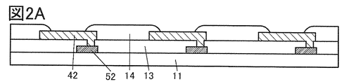
- the partition wall 14 is formed so as to cover the end portion of the conductive layer 42 (FIG. 2A).
- a film 31A to be the light emitting layer 31 a film 60A to be the conductive layer 60, and a film 63A to be the insulating layer 63 are formed in order (FIG. 2B).
- the film 31A can be formed by a method such as a thin film deposition method, a coating method, a printing method, and a ejection method.
- a thin-film deposition method that does not use a fine metal mask can be used.
- the film 60A can be formed by a method such as a vapor deposition method or a sputtering method.
- the film 63A can be formed by a method such as an ALD method, a CVD method, or a sputtering method.
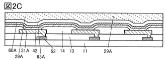
- the resist 29A is applied onto the film 63A (FIG. 2C).
- the resist 29A can be applied by using a spin coating method, a spray coating method, or the like.
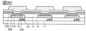
- the resist 29A is exposed and the resist 29A is processed. As a result, the resist mask 29B is formed (FIG. 2D).
- the resist mask 29B has a region overlapping with the conductive layer 42.
- the film 63A, the film 60A, and the film 31A are etched using the resist mask 29B as a mask.
- the island-shaped insulating layer 63, the conductive layer 60, and the light emitting layer 31 are formed (FIG. 3A).
- the etching can be, for example, wet etching or dry etching.
- the film 63A, the film 60A, and the film 31A are etched not only in the vertical direction but also in the horizontal direction. Therefore, the end portion of the insulating layer 63, the end portion of the conductive layer 60, and the end portion of the light emitting layer 31 can be configured to be located inside the end portion of the resist mask 29B. At least one of the end of the insulating layer 63, the end of the conductive layer 60, and the end of the light emitting layer 31 may be located outside the end of the resist mask 29B. For example, the end portion of the light emitting layer 31 may be located outside the end portion of the resist mask 29B.
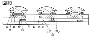
- the substrate 11 is heated.
- the resist mask 29B is softened and deformed into a convex shape.
- the lens 29 is formed by deforming the resist mask 29B into a convex shape (FIG. 3B).
- the insulating layer 21 is formed on the lens 29 and the partition wall 14 (FIG. 3C).
- the insulating layer 21 is preferably formed so as to have a region in contact with the upper surface of the lens 29, the side surface of the insulating layer 63, the side surface of the conductive layer 60, and the side surface of the light emitting layer 31.
- the end portion 32 of the lens 29 is located outside the end portion of the insulating layer 63, the end portion of the conductive layer 60, and the end portion of the light emitting layer 31.
- the insulating layer 21 is an insulating film having a high covering property. Therefore, it is preferable that the insulating layer 21 is formed by, for example, the ALD method.
- the colored layer 25R, the colored layer 25G, the colored layer 25B, and the light-shielding layer 45 are formed on the substrate 12 (FIG. 3D).
- the insulating layer 21, the colored layer 25R, the colored layer 25G, the colored layer 25B, and the light-shielding layer 45 are bonded together by the adhesive layer 33.
- the adhesive layer 33 can be formed by a screen printing method, a dispensing method, or the like. From the above, the display device 10 shown in FIG. 1 can be manufactured.
- the island-shaped insulating layer 63, the conductive layer 60, and the light emitting layer 31 are formed by etching using the resist mask 29B as a mask, and then the substrate 11 is heated to heat the lens. Form 29. Therefore, for example, the manufacturing process can be simplified as compared with the case where the resist mask 29B is removed to form the lens 29. From the above, the display device can be manufactured by a simple method according to the method for manufacturing the display device according to one aspect of the present invention. Therefore, the display device according to one aspect of the present invention can be an inexpensive display device.
- FIG. 4 is a cross-sectional view showing a configuration example of the display device 10.
- FIG. 4 shows a more specific configuration example of the display device 10 shown in FIG.
- FIG. 4 shows a configuration example of the display unit 215, the drive circuit 201, and the like.
- the display device 10 shown in FIG. 4 has an electrode 4015, and the electrode 4015 is electrically connected to a terminal of the FPC 4018 via an anisotropic conductive layer 4019. Further, in FIG. 4, the electrode 4015 is electrically connected to the wiring 4014 at the openings formed in the insulating layer 4112, the insulating layer 4111, and the insulating layer 4110.
- the electrode 4015 is formed of the same conductive layer as the conductive layer 42, and the wiring 4014 is formed of the same conductive layer as the transistor 52 and the source electrode and drain electrode of the transistor 4011.
- FIG. 4 illustrates the transistor 52 included in the display unit 215 and the transistor 4011 included in the drive circuit 201. is doing.
- the bottom gate type transistor is illustrated as the transistor 52 and the transistor 4011 in FIG. 4, it may be a top gate type transistor.
- the insulating layer 4112 is provided on the transistor 52 and on the transistor 4011. Further, a partition wall 14 is formed on the insulating layer 4112.
- the transistor 52 and the transistor 4011 are provided on the insulating layer 4102. Further, the transistor 52 and the transistor 4011 have an electrode 4017 formed on the insulating layer 4111.
- the electrode 4017 can function as a backgate electrode.
- the display device 10 shown in FIG. 4 has a capacity of 4020.
- the capacitance 4020 has an electrode 4021 formed in the same step as the gate electrode of the transistor 52, and an electrode formed in the same step as the source electrode and the drain electrode.
- the respective electrodes are overlapped with each other via the insulating layer 4103.
- the display device shown in FIG. 4 has an insulating layer 4111 and an insulating layer 4102.
- an insulating layer that does not easily transmit impurity elements is used as the insulating layer 4111 and the insulating layer 4102.
- sandwiching the transistor between the insulating layer 4111 and the insulating layer 4102 it is possible to suppress the infiltration of impurities into the semiconductor layer from the outside.
- FIG. 4 shows a configuration in which the display unit 215 and the drive circuit 201 are sealed by the sealing material 4005 and the substrate 12.
- the sealing material 4005 a glass material such as a glass frit, a curable resin such as a two-component mixed resin that cures at room temperature, a photocurable resin, and a resin material such as a thermosetting resin can be used.
- the sealing material 4005 may contain a desiccant.
- an optical film such as a polarizing plate, a circular polarizing plate (including an elliptical polarizing plate), and a retardation plate ( ⁇ / 4 plate, ⁇ / 2 plate) is appropriately provided on the emission surface of the light emitting element 30. You may. Further, an antireflection film may be provided on the polarizing plate or the circular polarizing plate. For example, it is possible to apply an anti-glare treatment that can diffuse the reflected light due to the unevenness of the surface and reduce the reflection.
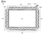
- FIG. 5A and 5B are diagrams showing a configuration example of the display device 10.
- a sealing material 4005 is provided so as to surround the display unit 215.
- Pixels 15 (pixels 15R, pixels 15G, and pixels 15B) shown in FIG. 1 and the like are arranged in a matrix on the display unit 215.
- the drive circuit 221, the drive circuit 231 and the drive circuit 232, and the drive circuit 241 each have a plurality of integrated circuits 4042 provided on the printed circuit board 4041.
- the integrated circuit 4042 is made of a single crystal semiconductor or a polycrystalline semiconductor.
- the drive circuit 201 shown in FIG. 4 may be a drive circuit 221 or a drive circuit 231 or a drive circuit 232 or a drive circuit 241.
- the integrated circuit 4042 included in the drive circuit 221 and the drive circuit 241 has a function of supplying a selection signal to the display unit 215.
- the integrated circuit 4042 included in the drive circuit 231 and the drive circuit 232 has a function of supplying an image signal to the display unit 215.
- the integrated circuit 4042 is mounted in a region different from the region surrounded by the sealing material 4005 on the substrate 11.
- connection method of the integrated circuit 4042 is not particularly limited, and a wire bonding method, a COG (Chip On Glass) method, a TCP (Tape Carrier Package) method, a COF (Chip On Film) method, or the like is used. Can be done.
- a wire bonding method a COG (Chip On Glass) method, a TCP (Tape Carrier Package) method, a COF (Chip On Film) method, or the like is used. Can be done.
- FIG. 5B shows an example of mounting the integrated circuit 4042 included in the drive circuit 231 and the drive circuit 232 by the COG method. Further, a part or the whole of the drive circuit can be integrally formed on the same substrate as the display unit 215 to form a system on panel.
- FIG. 5B shows an example in which the drive circuit 221 and the drive circuit 241 are formed on the same substrate as the display unit 215.
- the drive circuit By forming the drive circuit at the same time as the pixel circuit in the display unit 215, the number of parts can be reduced. Therefore, productivity can be increased.
- a sealing material 4005 is provided so as to surround the display unit 215 provided on the substrate 11, the drive circuit 221 and the drive circuit 241. Further, the substrate 12 is provided on the display unit 215, the drive circuit 221 and the drive circuit 241. Therefore, the display unit 215, the drive circuit 221 and the drive circuit 241 are sealed together with the light emitting element by the substrate 11, the sealing material 4005, and the substrate 12.
- FIG. 5B shows an example in which the drive circuit 231 and the drive circuit 232 are separately formed and mounted on the substrate 11, but the configuration is not limited to this.
- the drive circuit 221 may be separately formed and mounted.
- the display device 10 may include a panel in which a light emitting element is sealed, and a module in which an IC including a controller is mounted on the panel, for example.
- an input device can be provided on the substrate 12.
- the configuration in which the input device is provided in the display device 10 shown in FIG. 5A or FIG. 5B can function as a touch panel.
- the detection element (also referred to as a sensor element) included in the touch panel of one aspect of the present invention is not limited.
- various methods such as a capacitance method, a resistance film method, a surface acoustic wave method, an infrared method, an optical method, and a pressure sensitive method can be used.
- the capacitance method there are a surface type capacitance method, a projection type capacitance method and the like. Further, as the projection type capacitance method, there are a self-capacitance method, a mutual capacitance method and the like. It is preferable to use the mutual capacitance method because simultaneous multipoint detection is possible.
- the touch panel of one aspect of the present invention has a configuration in which a separately manufactured display device and a detection element are bonded together, a configuration in which electrodes and the like constituting the detection element are provided on one or both of a substrate supporting a light emitting element and a facing substrate, and the like. , Various configurations can be applied.
- FIG. 6A and 6B show an example of a touch panel.
- FIG. 6A is a perspective view of the touch panel 4210.
- the touch panel 4210 has an input device 4200.
- FIG. 6B is a schematic perspective view of the input device 4200. For the sake of clarity, only typical components are shown.
- the touch panel 4210 has a configuration in which a separately manufactured display device and a detection element are bonded together.
- the touch panel 4210 has an input device 4200 and a display device 10, and these are provided on top of each other.
- the display device 10 is not shown in FIG. 6A.
- the input device 4200 has a substrate 4263, an electrode 4227, an electrode 4228, a plurality of wirings 4237, a plurality of wirings 4238, and a plurality of wirings 4239.
- the electrode 4227 can be electrically connected to the wiring 4237 or the wiring 4239.
- the electrode 4228 can be electrically connected to the wiring 4239.
- the FPC 4272 is electrically connected to each of the plurality of wirings 4237, the plurality of wirings 4238, and the plurality of wirings 4239.
- IC4273 can be provided in FPC4272.
- a touch sensor may be provided between the substrate 11 and the substrate 12 of the display device 10.
- an optical touch sensor using a photoelectric conversion element as a detection element may be applied in addition to the capacitance type touch sensor.
- This embodiment can be carried out in combination with at least a part thereof as appropriate in combination with other embodiments described in the present specification.
- the display device of one aspect of the present invention can be manufactured by using various types of transistors such as a bottom gate type transistor and a top gate type transistor. Therefore, the material of the semiconductor layer to be used, the transistor structure, and the like can be easily replaced according to the existing production line.
- FIG. 7A1 is a cross-sectional view of a channel protection type transistor 810 which is a kind of bottom gate type transistor.
- the transistor 810 is formed on the substrate 771.
- the transistor 810 has an electrode 746 on the substrate 771 via an insulating layer 772.
- the semiconductor layer 742 is provided on the electrode 746 via the insulating layer 726.
- the electrode 746 can function as a gate electrode.
- the insulating layer 726 can function as a gate insulating layer.
- the insulating layer 741 is provided on the channel forming region of the semiconductor layer 742. Further, the electrode 744a and the electrode 744b are provided on the insulating layer 726 in contact with a part of the semiconductor layer 742.
- the electrode 744a can function as either a source electrode or a drain electrode.
- the electrode 744b can function as the other of the source electrode and the drain electrode. A part of the electrode 744a and a part of the electrode 744b are formed on the insulating layer 741.
- the insulating layer 741 can function as a channel protection layer. By providing the insulating layer 741 on the channel forming region, it is possible to prevent the semiconductor layer 742 from being exposed when the electrodes 744a and 744b are formed. Therefore, it is possible to prevent the channel formation region of the semiconductor layer 742 from being etched when the electrodes 744a and 744b are formed. According to one aspect of the present invention, a transistor having good electrical characteristics can be realized.
- the transistor 810 has an insulating layer 728 on the electrodes 744a, 744b and the insulating layer 741, and has an insulating layer 729 on the insulating layer 728.
- an oxide semiconductor When an oxide semiconductor is used for the semiconductor layer 742, a material capable of depriving a part of the semiconductor layer 742 of oxygen and causing oxygen deficiency is used at least in the portions of the electrodes 744a and 744b in contact with the semiconductor layer 742. Is preferable.
- the carrier concentration increases in the region where oxygen deficiency occurs in the semiconductor layer 742, and the region becomes n-type and becomes an n-type region (n + layer). Therefore, the region can function as a source region or a drain region.
- tungsten, titanium and the like can be mentioned as an example of a material capable of depriving the semiconductor layer 742 of oxygen and causing oxygen deficiency.
- the contact resistance between the electrodes 744a and 744b and the semiconductor layer 742 can be reduced. Therefore, the electrical characteristics of the transistor such as the field effect mobility and the threshold voltage can be improved.
- the semiconductor layer 742 When a semiconductor such as silicon is used for the semiconductor layer 742, it is preferable to provide a layer that functions as an n-type semiconductor or a p-type semiconductor between the semiconductor layer 742 and the electrode 744a and between the semiconductor layer 742 and the electrode 744b.
- the layer that functions as an n-type semiconductor or a p-type semiconductor can function as a source region or a drain region of a transistor.
- the insulating layer 729 is preferably formed by using a material having a function of preventing or reducing the diffusion of impurities from the outside to the transistor.
- the insulating layer 729 may be omitted if necessary.
- the transistor 811 shown in FIG. 7A2 differs from the transistor 810 in that the insulating layer 729 has an electrode 723 that can function as a back gate electrode.
- the electrode 723 can be formed by the same material and method as the electrode 746.
- the back gate electrode is formed of a conductive layer, and is arranged so as to sandwich the channel forming region of the semiconductor layer between the gate electrode and the back gate electrode. Therefore, the back gate electrode can function in the same manner as the gate electrode.
- the potential of the back gate electrode may be the same potential as that of the gate electrode, may be a ground potential (GND potential), or may be an arbitrary potential.
- the threshold voltage of the transistor can be changed by changing the potential of the back gate electrode independently without interlocking with the gate electrode.
- Both the electrode 746 and the electrode 723 can function as a gate electrode. Therefore, the insulating layer 726, the insulating layer 728, and the insulating layer 729 can each function as a gate insulating layer.
- the electrode 723 may be provided between the insulating layer 728 and the insulating layer 729.
- the other is referred to as a "back gate electrode".
- the electrode 746 when the electrode 723 is referred to as a "gate electrode”, the electrode 746 is referred to as a "back gate electrode”.
- the transistor 811 can be considered as a kind of top gate type transistor.
- either one of the electrode 746 and the electrode 723 may be referred to as a "first gate electrode”, and the other may be referred to as a "second gate electrode".
- the region in which the carriers flow in the semiconductor layer 742 becomes larger in the film thickness direction.
- the amount of carrier movement increases.
- the on-current of the transistor 811 becomes large, and the field effect mobility becomes high.
- the transistor 811 is a transistor having a large on-current with respect to the occupied area. That is, the occupied area of the transistor 811 can be reduced with respect to the required on-current. According to one aspect of the present invention, the occupied area of the transistor can be reduced. Therefore, according to one aspect of the present invention, it is possible to realize a display device having fine pixels, so that a high-definition display device can be realized.
- the gate electrode and the back gate electrode are formed of a conductive layer, it has a function of preventing an electric field generated outside the transistor from acting on the semiconductor layer on which a channel is formed (particularly, an electric field shielding function against static electricity). ..
- the back gate electrode By forming the back gate electrode larger than the semiconductor layer and covering the semiconductor layer with the back gate electrode, the electric field shielding function can be enhanced.
- the back gate electrode by forming the back gate electrode with a conductive film having a light-shielding property, it is possible to prevent light from being incident on the semiconductor layer from the back gate electrode side. Therefore, it is possible to prevent photodegradation of the semiconductor layer and prevent deterioration of electrical characteristics such as a shift of the threshold voltage of the transistor.
- a transistor with good reliability can be realized.
- a display device with good reliability can be realized.
- FIG. 7B1 shows a cross-sectional view of a channel protection type transistor 820, which is one of the bottom gate type transistors.
- the transistor 820 has almost the same structure as the transistor 810, except that the insulating layer 741 covers the end portion of the semiconductor layer 742. Further, the semiconductor layer 742 and the electrode 744a are electrically connected to each other in the opening formed by selectively removing a part of the insulating layer 741 overlapping the semiconductor layer 742. Further, the semiconductor layer 742 and the electrode 744b are electrically connected to each other in another opening formed by selectively removing a part of the insulating layer 741 overlapping the semiconductor layer 742.
- the region of the insulating layer 741 that overlaps the channel forming region can function as a channel protection layer.
- the transistor 821 shown in FIG. 7B2 differs from the transistor 820 in that the insulating layer 729 has an electrode 723 that can function as a back gate electrode.
- the insulating layer 741 By providing the insulating layer 741, it is possible to prevent the semiconductor layer 742 from being exposed when the electrodes 744a and 744b are formed. Therefore, it is possible to prevent the semiconductor layer 742 from being thinned when the electrodes 744a and 744b are formed.
- the transistor 820 and the transistor 821 have a longer distance between the electrode 744a and the electrode 746 and a distance between the electrode 744b and the electrode 746 than the transistor 810 and the transistor 811. Therefore, the parasitic capacitance generated between the electrode 744a and the electrode 746 can be reduced. In addition, the parasitic capacitance generated between the electrode 744b and the electrode 746 can be reduced. According to one aspect of the present invention, a transistor having good electrical characteristics can be realized.
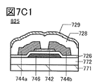
- the transistor 825 shown in FIG. 7C1 is a channel etching type transistor which is one of the bottom gate type transistors.
- the transistor 825 forms the electrodes 744a and 744b without using the insulating layer 741. Therefore, a part of the semiconductor layer 742 exposed at the time of forming the electrode 744a and the electrode 744b may be etched. On the other hand, since the insulating layer 741 is not provided, the productivity of the transistor can be improved.
- the transistor 826 shown in FIG. 7C2 differs from the transistor 820 in that the insulating layer 729 has an electrode 723 that can function as a back gate electrode.
- the transistor 842 exemplified in FIG. 8A1 is one of the top gate type transistors.
- the transistor 842 differs from the transistor 810, the transistor 811, the transistor 820, the transistor 821, the transistor 825, and the transistor 826 in that the electrode 744a and the electrode 744b are formed after the insulating layer 729 is formed.
- the electrodes 744a and 744b are electrically connected to the semiconductor layer 742 at the openings formed in the insulating layer 728 and the insulating layer 729.
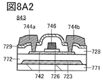
- the transistor 843 shown in FIG. 8A2 differs from the transistor 842 in that it has an electrode 723.
- Transistor 843 has an electrode 723 formed on the substrate 771.
- the electrode 723 has a region overlapping the semiconductor layer 742 via the insulating layer 772.
- the electrode 723 can function as a backgate electrode.
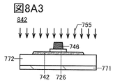
- Transistor 842 has a region where the insulating layer 726 extends beyond the end of the electrode 746.
- the impurity concentration in the region where the impurity 755 is introduced via the insulating layer 726 of the semiconductor layer 742 is smaller than that in the region where the impurity 755 is introduced without passing through the insulating layer 726. Therefore, in the semiconductor layer 742, an LDD (Lightly Doped Drain) region is formed in a region that does not overlap with the electrode 746. The above is the same for the transistor 843.
- the insulating layer 726 in the region not overlapping with the electrode 746 may be completely removed. Further, the insulating layer 726 may be left as in the transistor 846 shown in FIG. 8C1 and the transistor 847 shown in FIG. 8C2.
- Transistors 844 to 847 can also form an impurity region in the semiconductor layer 742 in a self-aligned manner by introducing the impurity 755 into the semiconductor layer 742 using the electrode 746 as a mask after forming the electrode 746. .. According to one aspect of the present invention, a transistor having good electrical characteristics can be realized. Further, according to one aspect of the present invention, a high-definition display device can be realized.
- This embodiment can be carried out in combination with at least a part thereof as appropriate in combination with other embodiments described in the present specification.
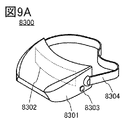
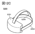
- 9A and 9B show the appearance of the head-mounted display 8300.
- the head-mounted display 8300 has a housing 8301, a display unit 8302, an operation button 8303, and a band-shaped fixture 8304.
- the operation button 8303 has a function as, for example, a power button. Further, it may have a button in addition to the operation button 8303.
- the lens 8305 may be provided between the display unit 8302 and the position of the user's eyes.
- the lens 8305 allows the user to magnify and view the display unit 8302, which further enhances the sense of presence.
- a dial 8306 that changes the position of the lens for diopter adjustment may be provided.
- a display device can be applied to the display unit 8302. Since the display device of one aspect of the present invention has extremely high definition, even if the display device is magnified using the lens 8305 as shown in FIG. 9C, the pixels are not visually recognized by the user, and a more realistic image can be obtained. Can be displayed.
- 9A to 9C show an example in which one display unit 8302 is provided. With such a configuration, the number of parts can be reduced.
- the display unit 8302 can display two images, one for the right eye and the other for the left eye, side by side in the two left and right areas, respectively. This makes it possible to display a stereoscopic image using binocular parallax.
- one image that can be visually recognized by both eyes may be displayed over the entire area of the display unit 8302. This makes it possible to display a panoramic image over both ends of the field of view, which enhances the sense of reality.
- the head-mounted display 8300 has a mechanism for changing the curvature of the display unit 8302 to an appropriate value according to the size of the user's head, the position of the eyes, and the like.
- the user may adjust the curvature of the display unit 8302 by operating the dial 8307 for adjusting the curvature of the display unit 8302.
- the housing 8301 is provided with a sensor (for example, a camera, a contact sensor, a non-contact sensor, etc.) that detects the size of the user's head, the position of the eyes, etc., and the display unit 8302 is based on the detection data of the sensor. It may have a mechanism for adjusting the curvature of.
- the dial 8306 may have a function of adjusting the angle of the lens.
- FIGE and 9F show an example including a drive unit 8308 that controls the curvature of the display unit 8302.
- the drive unit 8308 is fixed to at least a part of the display unit 8302.
- the drive unit 8308 has a function of deforming the display unit 8302 by deforming or moving a portion fixed to the display unit 8302.
- FIG. 9E is a schematic view of a user 8310 having a relatively large head size wearing the housing 8301. At this time, the shape of the display unit 8302 is adjusted by the drive unit 8308 so that the curvature is relatively small (the radius of curvature is large).
- FIG. 9F shows a case where the user 8311, whose head size is smaller than that of the user 8310, is wearing the housing 8301.
- the distance between the eyes of the user 8311 is narrower than that of the user 8310.
- the shape of the display unit 8302 is adjusted by the drive unit 8308 so that the curvature of the display unit 8302 becomes large (the radius of curvature becomes small).
- the position and shape of the display unit 8302 in FIG. 9E are shown by broken lines.
- the head-mounted display 8300 has a mechanism for adjusting the curvature of the display unit 8302, so that it is possible to provide an optimum display to users of various ages and sexes.
- the shaking can be expressed by vibrating the curvature of the display unit 8302.
- various effects can be produced according to the scene in the content, and a new experience can be provided to the user.
- interlocking with the vibration module provided in the housing 8301 it is possible to display with a higher sense of presence.
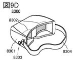
- the head-mounted display 8300 may have two display units 8302 as shown in FIG. 9D.
- the user can see one display unit per eye. This makes it possible to display a high-resolution image even when performing a three-dimensional display using parallax, for example.
- the display unit 8302 is curved in an arc shape centered substantially on the user's eyes. As a result, the distance from the user's eyes to the display surface of the display unit becomes constant, so that the user can see a more natural image. Further, even if the brightness and chromaticity of the light from the display unit change depending on the viewing angle, the user's eyes are positioned in the normal direction of the display surface of the display unit, so that the user's eyes are substantially located. The effect can be ignored. Therefore, the display unit 8302 can display a more realistic image.
- This embodiment can be carried out in combination with at least a part thereof as appropriate in combination with other embodiments described in the present specification.
- the display module 6000 shown in FIG. 10A has a display device 6006, a frame 6009, a printed circuit board 6010, and a battery 6011 to which an FPC 6005 is connected between the upper cover 6001 and the lower cover 6002.
- a display device manufactured using one aspect of the present invention can be used for the display device 6006.
- the display device 6006 it is possible to realize a display module having extremely low power consumption.
- the shape and dimensions of the upper cover 6001 and the lower cover 6002 can be appropriately changed according to the size of the display device 6006.
- the display device 6006 may have a function as a touch panel.
- the frame 6009 may have a protective function of the display device 6006, a function of blocking electromagnetic waves generated by the operation of the printed circuit board 6010, a function of a heat sink, and the like.
- the printed circuit board 6010 includes a power supply circuit, a signal processing circuit for outputting a video signal and a clock signal, a battery control circuit, and the like.
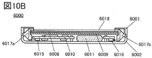
- FIG. 10B is a schematic cross-sectional view of the display module 6000 including an optical touch sensor.
- the display module 6000 has a light emitting unit 6015 and a light receiving unit 6016 provided on the printed circuit board 6010. Further, the area surrounded by the upper cover 6001 and the lower cover 6002 has a pair of light guides (light guide 6017a, light guide 6017b).
- the display device 6006 is provided so as to overlap the printed circuit board 6010 and the battery 6011 with the frame 6009 interposed therebetween.
- the display device 6006 and the frame 6009 are fixed to the light guide unit 6017a and the light guide unit 6017b.
- the light 6018 emitted from the light emitting unit 6015 passes through the upper part of the display device 6006 by the light guide unit 6017a, passes through the light guide unit 6017b, and reaches the light receiving unit 6016.
- the touch operation can be detected by blocking the light 6018 by a detected object such as a finger or a stylus.
- a plurality of light emitting units 6015 are provided, for example, along two adjacent sides of the display device 6006.
- a plurality of light receiving units 6016 are provided at positions facing the light emitting unit 6015. As a result, it is possible to acquire information on the position where the touch operation is performed.
- a light source of an LED element can be used, and it is particularly preferable to use a light source that emits infrared rays.
- a photoelectric conversion element that receives the light emitted by the light emitting unit 6015 and converts it into an electric signal can be used.
- a photodiode capable of receiving infrared rays can be used.
- the light emitting unit 6015 and the light receiving unit 6016 can be arranged under the display device 6006 by the light guide unit 6017a and the light receiving unit 6017b that transmit the light 6018, and the external light reaches the light receiving unit 6016 and touches. It is possible to prevent the sensor from malfunctioning. In particular, if a resin that absorbs visible light and transmits infrared rays is used, the malfunction of the touch sensor can be suppressed more effectively.
- This embodiment can be carried out in combination with at least a part thereof as appropriate in combination with other embodiments described in the present specification.
- the electronic device 6500 shown in FIG. 11A is a portable information terminal that can be used as a smartphone.
- the electronic device 6500 includes a housing 6501, a display unit 6502, a power button 6503, a button 6504, a speaker 6505, a microphone 6506, a camera 6507, a light source 6508, and the like.
- the display unit 6502 has a touch panel function.
- a display device can be applied to the display unit 6502. As a result, a high-quality image can be displayed on the display unit 6502.
- FIG. 11B is a schematic cross-sectional view including an end portion of the housing 6501 on the microphone 6506 side.
- a translucent protective member 6510 is provided on the display surface side of the housing 6501, and a display panel 6511, an optical member 6512, a touch sensor panel 6513, and a print are provided in a space surrounded by the housing 6501 and the protective member 6510.
- a substrate 6517, a battery 6518, and the like are arranged.
- a display panel 6511, an optical member 6512, and a touch sensor panel 6513 are fixed to the protective member 6510 by an adhesive layer (not shown).
- the FPC 6515 is connected to the folded portion.
- the IC6516 is mounted on the FPC6515. Further, the FPC 6515 is connected to a terminal provided on the printed circuit board 6517.
- This embodiment can be carried out in combination with at least a part thereof as appropriate in combination with other embodiments described in the present specification.
- the electronic device exemplified below is provided with a display device according to one aspect of the present invention in the display unit. Therefore, it is an electronic device that realizes high resolution. In addition, it is possible to make an electronic device that has both high resolution and a large screen.
- One aspect of the present invention includes a display device and at least one of an antenna, a battery, a housing, a camera, a speaker, a microphone, a touch sensor, and an operation button.
- the electronic device of one aspect of the present invention may have a secondary battery, and it is preferable that the secondary battery can be charged by using non-contact power transmission.
- the secondary battery examples include a lithium ion secondary battery such as a lithium polymer battery (lithium ion polymer battery) using a gel-like electrolyte, a nickel hydrogen battery, a nicad battery, an organic radical battery, a lead storage battery, an air secondary battery, and nickel.
- a lithium ion secondary battery such as a lithium polymer battery (lithium ion polymer battery) using a gel-like electrolyte, a nickel hydrogen battery, a nicad battery, an organic radical battery, a lead storage battery, an air secondary battery, and nickel.
- Examples include a zinc battery and a silver-zinc battery.
- the electronic device of one aspect of the present invention may have an antenna.
- the display unit can display images, information, and the like.
- the antenna may be used for non-contact power transmission.
- An image having a resolution of, for example, full high-definition, 4K2K, 8K4K, 16K8K, or higher can be displayed on the display unit of the electronic device of one aspect of the present invention.
- Electronic devices include, for example, electronic devices with relatively large screens such as television devices, notebook personal computers, monitor devices, digital signage, pachinko machines, and game machines, as well as digital cameras, digital video cameras, and digital devices. Examples thereof include a photo frame, a mobile phone, a portable game machine, a mobile information terminal, a sound reproduction device, and the like.
- An electronic device to which one aspect of the present invention is applied can be incorporated along a flat surface or a curved surface of an inner wall or an outer wall of a building such as a house or a building, or an interior or exterior of an automobile or the like.
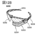
- FIG. 12A is a diagram showing the appearance of the camera 8000 with the finder 8100 attached.
- the camera 8000 has a housing 8001, a display unit 8002, an operation button 8003, a shutter button 8004, and the like.
- a detachable lens 8006 is attached to the camera 8000.
- the lens 8006 and the housing may be integrated.
- the camera 8000 can take an image by pressing the shutter button 8004 or touching the display unit 8002 that functions as a touch panel.
- the housing 8001 has a mount having electrodes, and in addition to the finder 8100, for example, a strobe device can be connected to the housing 8001.
- the finder 8100 includes a housing 8101, a display unit 8102, a button 8103, and the like.
- the housing 8101 is attached to the camera 8000 by a mount that engages with the mount of the camera 8000.
- the finder 8100 can display, for example, an image received from the camera 8000 on the display unit 8102.
- the button 8103 has a function as, for example, a power button.
- the display device of one aspect of the present invention can be applied to the display unit 8002 of the camera 8000 and the display unit 8102 of the finder 8100. As a result, a high-quality image can be displayed on the display unit 8002 and the display unit 8102.
- the camera may be a camera 8000 with a built-in finder.
- FIG. 12B is a diagram showing the appearance of the head-mounted display 8200.
- the head-mounted display 8200 has a mounting unit 8201, a lens 8202, a main body 8203, a display unit 8204, a cable 8205, and the like. Further, the battery 8206 is built in the mounting portion 8201.
- the cable 8205 supplies electric power from the battery 8206 to the main body 8203.
- the main body 8203 is provided with, for example, a wireless receiver, and the received video information can be displayed on the display unit 8204. Further, the main body 8203 is provided with a camera, and information on the movement of the user's eyeball or eyelid can be used as an input means.
- the mounting portion 8201 may be provided with a plurality of electrodes capable of detecting the current flowing with the movement of the user's eyeball at a position touching the user, and may have a function of recognizing the line of sight. Further, it may have a function of monitoring the pulse of the user by the current flowing through the electrode. Further, the mounting unit 8201 may have various sensors such as a temperature sensor, a pressure sensor, and an acceleration sensor, and has a function of displaying the biometric information of the user on the display unit 8204 and a head of the user. It may have a function of changing the image displayed on the display unit 8204 according to the movement.
- a display device can be applied to the display unit 8204. As a result, a high-quality image can be displayed on the display unit 8204.
- the head-mounted display 8300 has a housing 8301, a display unit 8302, a band-shaped fixture 8304, and a pair of lenses 8305.
- the user can visually recognize the display of the display unit 8302 through the lens 8305. It is preferable to arrange the display unit 8302 in a curved manner because the user can feel a high sense of presence. Further, by visually recognizing another image displayed in a different area of the display unit 8302 through the lens 8305, for example, a three-dimensional display using parallax can be performed.
- the configuration is not limited to the configuration in which one display unit 8302 is provided, and two display units 8302 may be provided and one display unit may be arranged for one eye of the user.
- the display device of one aspect of the present invention can be applied to the display unit 8302. Since the display device having the semiconductor device of one aspect of the present invention has extremely high definition, even if the display device is magnified by using the lens 8305 as shown in FIG. 12E, the pixels are not visually recognized by the user, and the feeling of reality is increased. It is possible to display high-quality images.
- the electronic devices shown in FIGS. 13A to 13G include a housing 9000, a display unit 9001, a speaker 9003, an operation key 9005 (including a power switch or an operation switch), a connection terminal 9006, and a sensor 9007 (force, displacement, position, speed). , Acceleration, angular velocity, rotation speed, distance, light, liquid, magnetism, temperature, chemical substance, voice, time, hardness, electric field, current, voltage, power, radiation, flow rate, humidity, gradient, vibration, odor or infrared It has a function to perform), a microphone 9008, and the like.
- the electronic devices shown in FIGS. 13A to 13G have various functions. For example, a function to display various information (still images, moving images, text images, etc.) on the display unit, a touch panel function, a function to display a calendar, date or time, etc., a function to control processing by various software (programs), It can have a wireless communication function, a function of reading out and processing a program or data recorded on a recording medium, and the like.
- the functions of electronic devices are not limited to these, and can have various functions.
- the electronic device may have a plurality of display units.
- the electronic device even if the electronic device is provided with a camera or the like, it has a function of shooting a still image or a moving image and saving it on a recording medium (external or built in the camera), a function of displaying the shot image on a display unit, and the like. good.
- FIGS. 13A to 13G The details of the electronic devices shown in FIGS. 13A to 13G will be described below.
- FIG. 13A is a perspective view showing the television device 9100.
- the television device 9100 can incorporate a large screen, for example, a display unit 9001 having a size of 50 inches or more, or 100 inches or more.
- FIG. 13B is a perspective view showing a mobile information terminal 9101.
- the mobile information terminal 9101 can be used as, for example, a smartphone.
- the mobile information terminal 9101 may be provided with a speaker 9003, a connection terminal 9006, a sensor 9007, and the like. Further, the mobile information terminal 9101 can display characters, image information, and the like on a plurality of surfaces thereof.
- FIG. 13B shows an example in which three icons 9050 are displayed. Further, the information 9051 indicated by the broken line rectangle can be displayed on the other surface of the display unit 9001.
- Examples of information 9051 include notification of incoming calls such as e-mail, SNS, and telephone, title of e-mail or SNS, sender name, date and time, time, remaining amount of battery, strength of antenna reception, and the like.
- the icon 9050 or the like may be displayed at the position where the information 9051 is displayed.
- FIG. 13C is a perspective view showing a mobile information terminal 9102.
- the mobile information terminal 9102 has a function of displaying information on three or more surfaces of the display unit 9001.
- information 9052, information 9053, and information 9054 are displayed on different surfaces.
- the user can check the information 9053 displayed at a position that can be observed from above the mobile information terminal 9102 with the mobile information terminal 9102 stored in the chest pocket of the clothes.
- the user can check the display without taking out the mobile information terminal 9102 from the pocket, and can determine, for example, whether or not to receive a call.
- FIG. 13D is a perspective view showing a wristwatch-type portable information terminal 9200.
- the mobile information terminal 9200 can be used, for example, as a smart watch (registered trademark).
- the display unit 9001 is provided with a curved display surface, and can display along the curved display surface.
- the mobile information terminal 9200 can also make a hands-free call by, for example, communicating with a headset capable of wireless communication.
- the mobile information terminal 9200 can also perform data transmission or charge with other information terminals by means of the connection terminal 9006.
- the charging operation may be performed by wireless power supply.
- FIGS. 13E and 13G are perspective views showing a foldable mobile information terminal 9201. Further, FIG. 13E is a perspective view of a state in which the mobile information terminal 9201 is expanded, FIG. 13G is a folded state, and FIG. 13F is a perspective view of a state in which one of FIGS. 13E and 13G is in the process of changing to the other.
- the mobile information terminal 9201 is excellent in portability in the folded state, and is excellent in the listability of the display due to the wide seamless display area in the unfolded state.
- the display unit 9001 included in the portable information terminal 9201 is supported by three housings 9000 connected by a hinge 9055. For example, the display unit 9001 can be bent with a radius of curvature of 1 mm or more and 150 mm or less.
- FIG. 14A shows an example of a television device.
- the display unit 7500 is incorporated in the housing 7101.
- a configuration in which the housing 7101 is supported by the stand 7103 is shown.
- the operation of the television device 7100 shown in FIG. 14A can be performed by the operation switch provided in the housing 7101 or the remote control operation machine 7111 which is a separate body.
- a touch panel may be applied to the display unit 7500, and the television device 7100 may be operated by touching the touch panel.
- the remote controller 7111 may have a display unit in addition to the operation buttons.
- the television device 7100 may have a receiver for television broadcasting or a communication device for network connection.
- FIG. 14B shows a notebook personal computer 7200.
- the notebook personal computer 7200 has a housing 7211, a keyboard 7212, a pointing device 7213, an external connection port 7214, and the like.
- a display unit 7500 is incorporated in the housing 7211.
- FIGS 14C and 14D show an example of digital signage (electronic signage).
- the digital signage 7300 shown in FIG. 14C has a housing 7301, a display unit 7500, a speaker 7303, and the like. Further, it may have an LED lamp, an operation key (including a power switch or an operation switch), a connection terminal, various sensors, a microphone, and the like.
- FIG. 14D is a digital signage 7400 attached to a columnar pillar 7401.
- the digital signage 7400 has a display unit 7500 provided along the curved surface of the pillar 7401.
- a touch panel to the display unit 7500 so that the user can operate it.
- it can be used not only for advertising purposes but also for providing information requested by users such as route information, traffic information, and guidance information for commercial facilities.
- the digital signage 7300 or the digital signage 7400 can be linked with the information terminal 7311 such as a smartphone owned by the user by wireless communication.
- the information of the advertisement displayed on the display unit 7500 can be displayed on the screen of the information terminal 7311. Further, the display of the display unit 7500 can be switched by operating the information terminal 7311.
- the digital signage 7300 or the digital signage 7400 can be made to execute a game using the information terminal 7311 as an operating means (controller). As a result, an unspecified number of users can participate in and enjoy the game at the same time.
- a display device can be applied to the display unit 7500 in FIGS. 14A to 14D. As a result, a high-quality image can be displayed on the display unit 7500.
- the electronic device of the present embodiment is configured to have a display unit
- one aspect of the present invention can be applied to an electronic device having no display unit.
- This embodiment can be carried out in combination with at least a part thereof as appropriate in combination with other embodiments described in the present specification.
Landscapes
- Engineering & Computer Science (AREA)
- Manufacturing & Machinery (AREA)
- Physics & Mathematics (AREA)
- General Physics & Mathematics (AREA)
- Theoretical Computer Science (AREA)
- Microelectronics & Electronic Packaging (AREA)
- Electroluminescent Light Sources (AREA)
- Devices For Indicating Variable Information By Combining Individual Elements (AREA)
- Optical Filters (AREA)
Priority Applications (3)
| Application Number | Priority Date | Filing Date | Title |
|---|---|---|---|
| JP2022567710A JP7756657B2 (ja) | 2020-12-07 | 2021-11-24 | 表示装置 |
| US18/265,090 US20240065077A1 (en) | 2020-12-07 | 2021-11-24 | Display Device, Method For Manufacturing Display Device, and Electronic Device |
| JP2025169317A JP2025188132A (ja) | 2020-12-07 | 2025-10-07 | 表示装置 |
Applications Claiming Priority (2)
| Application Number | Priority Date | Filing Date | Title |
|---|---|---|---|
| JP2020-202400 | 2020-12-07 | ||
| JP2020202400 | 2020-12-07 |
Publications (1)
| Publication Number | Publication Date |
|---|---|
| WO2022123379A1 true WO2022123379A1 (ja) | 2022-06-16 |
Family
ID=81974203
Family Applications (1)
| Application Number | Title | Priority Date | Filing Date |
|---|---|---|---|
| PCT/IB2021/060903 Ceased WO2022123379A1 (ja) | 2020-12-07 | 2021-11-24 | 表示装置、表示装置の作製方法、及び電子機器 |
Country Status (3)
| Country | Link |
|---|---|
| US (1) | US20240065077A1 (https=) |
| JP (2) | JP7756657B2 (https=) |
| WO (1) | WO2022123379A1 (https=) |
Cited By (1)
| Publication number | Priority date | Publication date | Assignee | Title |
|---|---|---|---|---|
| CN116347919A (zh) * | 2023-04-21 | 2023-06-27 | 京东方科技集团股份有限公司 | 显示基板及制备方法、显示装置 |
Families Citing this family (1)
| Publication number | Priority date | Publication date | Assignee | Title |
|---|---|---|---|---|
| US12183294B1 (en) * | 2023-06-28 | 2024-12-31 | Yuanxu Semiconductor Technology (Wuxi) Co., Ltd | LED direct-view projection array light-emitting module and display screen |
Citations (8)
| Publication number | Priority date | Publication date | Assignee | Title |
|---|---|---|---|---|
| JP2003291404A (ja) * | 2002-04-01 | 2003-10-14 | Seiko Epson Corp | 有機elアレイ露光ヘッド及びそれを用いた画像形成装置 |
| JP2011060498A (ja) * | 2009-09-08 | 2011-03-24 | Panasonic Corp | 表示パネル、表示装置 |
| CN205723540U (zh) * | 2016-04-26 | 2016-11-23 | 张希娟 | 一种彩色微显示器件 |
| US20170062674A1 (en) * | 2015-08-31 | 2017-03-02 | Samsung Display Co., Ltd. | Display apparatus and manufacturing method thereof |
| US20190043842A1 (en) * | 2017-08-04 | 2019-02-07 | Au Optronics Corporation | Bi-directional optical module and transparent display apparatus using the same |
| JP2019133816A (ja) * | 2018-01-31 | 2019-08-08 | ソニーセミコンダクタソリューションズ株式会社 | 発光素子及び表示装置 |
| WO2020111101A1 (ja) * | 2018-11-30 | 2020-06-04 | ソニー株式会社 | 表示装置 |
| JP2020184481A (ja) * | 2019-05-09 | 2020-11-12 | セイコーエプソン株式会社 | 表示装置、および電子機器 |
Family Cites Families (3)
| Publication number | Priority date | Publication date | Assignee | Title |
|---|---|---|---|---|
| US11871641B2 (en) | 2018-07-27 | 2024-01-09 | Semiconductor Energy Laboratory Co., Ltd. | Display device, display module, and electronic device |
| CN118647237A (zh) | 2018-09-14 | 2024-09-13 | 株式会社半导体能源研究所 | 显示装置、显示模块及电子设备 |
| JP7380588B2 (ja) | 2018-11-27 | 2023-11-15 | ソニーグループ株式会社 | 発光素子、投影型表示装置及び面発光装置 |
-
2021
- 2021-11-24 US US18/265,090 patent/US20240065077A1/en active Pending
- 2021-11-24 JP JP2022567710A patent/JP7756657B2/ja active Active
- 2021-11-24 WO PCT/IB2021/060903 patent/WO2022123379A1/ja not_active Ceased
-
2025
- 2025-10-07 JP JP2025169317A patent/JP2025188132A/ja active Pending
Patent Citations (8)
| Publication number | Priority date | Publication date | Assignee | Title |
|---|---|---|---|---|
| JP2003291404A (ja) * | 2002-04-01 | 2003-10-14 | Seiko Epson Corp | 有機elアレイ露光ヘッド及びそれを用いた画像形成装置 |
| JP2011060498A (ja) * | 2009-09-08 | 2011-03-24 | Panasonic Corp | 表示パネル、表示装置 |
| US20170062674A1 (en) * | 2015-08-31 | 2017-03-02 | Samsung Display Co., Ltd. | Display apparatus and manufacturing method thereof |
| CN205723540U (zh) * | 2016-04-26 | 2016-11-23 | 张希娟 | 一种彩色微显示器件 |
| US20190043842A1 (en) * | 2017-08-04 | 2019-02-07 | Au Optronics Corporation | Bi-directional optical module and transparent display apparatus using the same |
| JP2019133816A (ja) * | 2018-01-31 | 2019-08-08 | ソニーセミコンダクタソリューションズ株式会社 | 発光素子及び表示装置 |
| WO2020111101A1 (ja) * | 2018-11-30 | 2020-06-04 | ソニー株式会社 | 表示装置 |
| JP2020184481A (ja) * | 2019-05-09 | 2020-11-12 | セイコーエプソン株式会社 | 表示装置、および電子機器 |
Cited By (1)
| Publication number | Priority date | Publication date | Assignee | Title |
|---|---|---|---|---|
| CN116347919A (zh) * | 2023-04-21 | 2023-06-27 | 京东方科技集团股份有限公司 | 显示基板及制备方法、显示装置 |
Also Published As
| Publication number | Publication date |
|---|---|
| JP2025188132A (ja) | 2025-12-25 |
| JPWO2022123379A1 (https=) | 2022-06-16 |
| JP7756657B2 (ja) | 2025-10-20 |
| US20240065077A1 (en) | 2024-02-22 |
Similar Documents
| Publication | Publication Date | Title |
|---|---|---|
| JP7292276B2 (ja) | 表示装置 | |
| JP7812952B2 (ja) | El表示装置、電子機器 | |
| KR20210043604A (ko) | 표시 장치, 표시 모듈, 및 전자 기기 | |
| KR102778385B1 (ko) | 표시 장치, 표시 모듈, 및 전자 기기 | |
| KR20180099666A (ko) | 표시 장치, 표시 모듈, 및 전자 기기 | |
| JP7757287B2 (ja) | 表示装置、電子機器、及びヘッドマウントディスプレイ | |
| JP2018032021A (ja) | 表示装置 | |
| JP2025188132A (ja) | 表示装置 | |
| JP7397957B2 (ja) | 半導体装置 | |
| JP2025078654A (ja) | 半導体装置 | |
| JP2022115080A (ja) | 表示装置 | |
| JP7766626B2 (ja) | 表示装置の作製方法 | |
| KR20230004267A (ko) | 표시 장치의 제작 방법 | |
| CN220359682U (zh) | 发光显示装置 | |
| US20240276834A1 (en) | Display Device, Method For Manufacturing Display Device, Display Module, and Electronic Device | |
| JP6822796B2 (ja) | 表示装置 | |
| US20220392982A1 (en) | Display apparatus and display system | |
| KR20230127224A (ko) | 표시 장치의 제작 방법 | |
| JP7812341B2 (ja) | 表示装置の作製方法 | |
| KR20210083284A (ko) | 표시 장치, 표시 모듈, 및 전자 기기 | |
| US20240224616A1 (en) | Display Apparatus | |
| CN117480881A (zh) | 显示装置、显示装置的制造方法、显示模块及电子设备 | |
| CN121646221A (zh) | 显示装置 | |
| CN118946211A (zh) | 显示装置 | |
| CN116367645A (zh) | 发光显示装置和用于制造发光显示装置的方法 |
Legal Events
| Date | Code | Title | Description |
|---|---|---|---|
| 121 | Ep: the epo has been informed by wipo that ep was designated in this application |
Ref document number: 21902805 Country of ref document: EP Kind code of ref document: A1 |
|
| ENP | Entry into the national phase |
Ref document number: 2022567710 Country of ref document: JP Kind code of ref document: A |
|
| WWE | Wipo information: entry into national phase |
Ref document number: 18265090 Country of ref document: US |
|
| NENP | Non-entry into the national phase |
Ref country code: DE |
|
| 122 | Ep: pct application non-entry in european phase |
Ref document number: 21902805 Country of ref document: EP Kind code of ref document: A1 |