WO2022091922A1 - 信号伝達装置、電子機器、車両 - Google Patents
信号伝達装置、電子機器、車両 Download PDFInfo
- Publication number
- WO2022091922A1 WO2022091922A1 PCT/JP2021/038884 JP2021038884W WO2022091922A1 WO 2022091922 A1 WO2022091922 A1 WO 2022091922A1 JP 2021038884 W JP2021038884 W JP 2021038884W WO 2022091922 A1 WO2022091922 A1 WO 2022091922A1
- Authority
- WO
- WIPO (PCT)
- Prior art keywords
- signal
- conductor
- potential
- pulse
- transformer
- Prior art date
- Legal status (The legal status is an assumption and is not a legal conclusion. Google has not performed a legal analysis and makes no representation as to the accuracy of the status listed.)
- Ceased
Links
Images


Classifications
-
- H—ELECTRICITY
- H02—GENERATION; CONVERSION OR DISTRIBUTION OF ELECTRIC POWER
- H02M—APPARATUS FOR CONVERSION BETWEEN AC AND AC, BETWEEN AC AND DC, OR BETWEEN DC AND DC, AND FOR USE WITH MAINS OR SIMILAR POWER SUPPLY SYSTEMS; CONVERSION OF DC OR AC INPUT POWER INTO SURGE OUTPUT POWER; CONTROL OR REGULATION THEREOF
- H02M1/00—Details of apparatus for conversion
- H02M1/08—Circuits specially adapted for the generation of control voltages for semiconductor devices incorporated in static converters
-
- H—ELECTRICITY
- H03—ELECTRONIC CIRCUITRY
- H03K—PULSE TECHNIQUE
- H03K17/00—Electronic switching or gating, i.e. not by contact-making and –breaking
- H03K17/51—Electronic switching or gating, i.e. not by contact-making and –breaking characterised by the components used
- H03K17/56—Electronic switching or gating, i.e. not by contact-making and –breaking characterised by the components used by the use, as active elements, of semiconductor devices
-
- H—ELECTRICITY
- H01—ELECTRIC ELEMENTS
- H01G—CAPACITORS; CAPACITORS, RECTIFIERS, DETECTORS, SWITCHING DEVICES, LIGHT-SENSITIVE OR TEMPERATURE-SENSITIVE DEVICES OF THE ELECTROLYTIC TYPE
- H01G4/00—Fixed capacitors; Processes of their manufacture
- H01G4/30—Stacked capacitors
-
- H—ELECTRICITY
- H02—GENERATION; CONVERSION OR DISTRIBUTION OF ELECTRIC POWER
- H02M—APPARATUS FOR CONVERSION BETWEEN AC AND AC, BETWEEN AC AND DC, OR BETWEEN DC AND DC, AND FOR USE WITH MAINS OR SIMILAR POWER SUPPLY SYSTEMS; CONVERSION OF DC OR AC INPUT POWER INTO SURGE OUTPUT POWER; CONTROL OR REGULATION THEREOF
- H02M7/00—Conversion of AC power input into DC power output; Conversion of DC power input into AC power output
- H02M7/42—Conversion of DC power input into AC power output without possibility of reversal
- H02M7/44—Conversion of DC power input into AC power output without possibility of reversal by static converters
- H02M7/48—Conversion of DC power input into AC power output without possibility of reversal by static converters using discharge tubes with control electrode or semiconductor devices with control electrode
- H02M7/53—Conversion of DC power input into AC power output without possibility of reversal by static converters using discharge tubes with control electrode or semiconductor devices with control electrode using devices of a triode or transistor type requiring continuous application of a control signal
- H02M7/537—Conversion of DC power input into AC power output without possibility of reversal by static converters using discharge tubes with control electrode or semiconductor devices with control electrode using devices of a triode or transistor type requiring continuous application of a control signal using semiconductor devices only, e.g. single switched pulse inverters
- H02M7/5387—Conversion of DC power input into AC power output without possibility of reversal by static converters using discharge tubes with control electrode or semiconductor devices with control electrode using devices of a triode or transistor type requiring continuous application of a control signal using semiconductor devices only, e.g. single switched pulse inverters in a bridge configuration
-
- H—ELECTRICITY
- H03—ELECTRONIC CIRCUITRY
- H03K—PULSE TECHNIQUE
- H03K5/00—Manipulating of pulses not covered by one of the other main groups of this subclass
- H03K5/22—Circuits having more than one input and one output for comparing pulses or pulse trains with each other according to input signal characteristics, e.g. slope, integral
- H03K5/24—Circuits having more than one input and one output for comparing pulses or pulse trains with each other according to input signal characteristics, e.g. slope, integral the characteristic being amplitude
-
- H—ELECTRICITY
- H03—ELECTRONIC CIRCUITRY
- H03K—PULSE TECHNIQUE
- H03K4/00—Generating pulses having essentially a finite slope or stepped portions
- H03K4/06—Generating pulses having essentially a finite slope or stepped portions having triangular shape
- H03K4/08—Generating pulses having essentially a finite slope or stepped portions having triangular shape having sawtooth shape
- H03K4/48—Generating pulses having essentially a finite slope or stepped portions having triangular shape having sawtooth shape using as active elements semiconductor devices
- H03K4/50—Generating pulses having essentially a finite slope or stepped portions having triangular shape having sawtooth shape using as active elements semiconductor devices in which a sawtooth voltage is produced across a capacitor
- H03K4/501—Generating pulses having essentially a finite slope or stepped portions having triangular shape having sawtooth shape using as active elements semiconductor devices in which a sawtooth voltage is produced across a capacitor the starting point of the flyback period being determined by the amplitude of the voltage across the capacitor, e.g. by a comparator
- H03K4/502—Generating pulses having essentially a finite slope or stepped portions having triangular shape having sawtooth shape using as active elements semiconductor devices in which a sawtooth voltage is produced across a capacitor the starting point of the flyback period being determined by the amplitude of the voltage across the capacitor, e.g. by a comparator the capacitor being charged from a constant-current source
-
- H—ELECTRICITY
- H04—ELECTRIC COMMUNICATION TECHNIQUE
- H04L—TRANSMISSION OF DIGITAL INFORMATION, e.g. TELEGRAPHIC COMMUNICATION
- H04L25/00—Baseband systems
- H04L25/02—Details ; arrangements for supplying electrical power along data transmission lines
- H04L25/0264—Arrangements for coupling to transmission lines
Definitions
- the inventions disclosed herein relate to signal transduction devices, electronic devices and vehicles.
- Patent Document 1 As an example of the prior art related to the above, Patent Document 1 can be mentioned.
- an analog signal for example, a monitored signal having voltage information or temperature information
- a triangular wave signal generated by charging / discharging a capacitor.
- the invention disclosed in the present specification is a signal transmission device and an electronic device capable of accurately converting an analog signal into a pulse signal and transmitting the analog signal in view of the above-mentioned problems found by the inventors of the present application. And to provide vehicles.
- the signal transmission device disclosed in the present specification has a capacitor in which a first capacitor element and a second capacitor element are connected in parallel so that nodes having different polarities are connected to each other.
- the analog signal is converted into a pulse signal and transmitted.
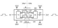
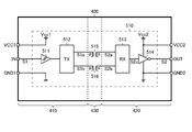
- FIG. 1 is a diagram showing a basic configuration of a signal transmission device.
- FIG. 2 is a diagram showing a basic structure of a transchip.
- FIG. 3 is a perspective view of a semiconductor device used as a 2-channel type transformer chip.
- FIG. 4 is a plan view of the semiconductor device shown in FIG.
- FIG. 5 is a plan view showing a layer in which a low potential coil is formed in the semiconductor device of FIG.
- FIG. 6 is a plan view showing a layer in which a high potential coil is formed in the semiconductor device of FIG.
- FIG. 7 is a cross-sectional view taken along the line VIII-VIII shown in FIG.
- FIG. 8 is a diagram showing an enlarged view (separated structure) of the region XIII shown in FIG. 7.
- FIG. 8 is a diagram showing an enlarged view (separated structure) of the region XIII shown in FIG. 7.
- FIG. 9 is a diagram schematically showing a layout example of the transformer chip.
- FIG. 10 is a diagram showing an embodiment of a signal transmission device.
- FIG. 11 is a diagram showing a configuration example of an isolated signal transmission circuit.
- FIG. 12 is a diagram showing an example of an isolated signal transmission operation.
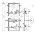
- FIG. 13 is a diagram showing a first embodiment of the insulation monitoring circuit.
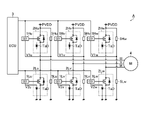
- FIG. 14 is a diagram showing an example of a first application of a signal transmission device.
- FIG. 15 is a diagram showing only one phase of the first application example extracted.
- FIG. 16 is a diagram showing a second embodiment of the insulation monitoring circuit.
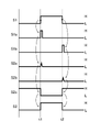
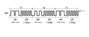
- FIG. 17 is a diagram showing a first example of time division control.
- FIG. 18 is a diagram showing a second example of time division control.
- FIG. 19 is a diagram showing an example of a second application of a signal transmission device.
- FIG. 20 is a diagram showing only one phase of the second application example extracted.
- FIG. 21 is a diagram showing an example of a third application of the signal transmission device.
- FIG. 22 is a diagram showing a configuration example of a pulse converter.
- FIG. 23 is a diagram showing a configuration example of a triangular wave oscillator.
- FIG. 24 is a diagram showing the voltage characteristics of the capacitor.
- FIG. 25 is a diagram showing an example of the element layout of the capacitor.
- FIG. 26 is a diagram showing a vertical cross section of Z1-Z2.
- FIG. 27 is a diagram showing the appearance of a vehicle on which an electronic device is mounted.
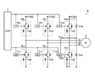
- FIG. 1 is a diagram showing a basic configuration of a signal transmission device.
- the signal transmission device 200 of this configuration example has the primary circuit system 200p to the secondary circuit system 200s while insulating between the primary circuit system 200p (VCC1-GND1 system) and the secondary circuit system 200s (VCC2-GND2 system).
- It is a semiconductor integrated circuit device (so-called insulated gate driver IC) that transmits a pulse signal to and drives a gate of a switch element (not shown) provided in the secondary circuit system 200s.
- the signal transmission device 200 includes a controller chip 210, a driver chip 220, and a transformer chip 230 sealed in a single package.
- the controller chip 210 is a semiconductor chip that operates by being supplied with a power supply voltage VCS1 (for example, a maximum of 7V based on GND1).
- VCS1 for example, a maximum of 7V based on GND1.
- the pulse transmission circuit 211 and the buffers 212 and 213 are integrated in the controller chip 210.
- the pulse transmission circuit 211 is a pulse generator that generates transmission pulse signals S11 and S21 according to the input pulse signal IN. More specifically, the pulse transmission circuit 211 performs pulse drive (single or multiple transmission pulse output) of the transmission pulse signal S11 when notifying that the input pulse signal IN is at a high level, and inputs the input pulse. When notifying that the signal IN is low level, the transmission pulse signal S21 is pulse-driven. That is, the pulse transmission circuit 211 pulse-drives either one of the transmission pulse signals S11 and S21 according to the logic level of the input pulse signal IN.
- the buffer 212 receives the input of the transmission pulse signal S11 from the pulse transmission circuit 211 and drives the transformer chip 230 (specifically, the transformer 231) in a pulse.
- the buffer 213 receives the input of the transmission pulse signal S21 from the pulse transmission circuit 211 and drives the transformer chip 230 (specifically, the transformer 232) in a pulse manner.
- the driver chip 220 is a semiconductor chip that operates by being supplied with a power supply voltage VCS2 (for example, a maximum of 30 V based on GND2).
- VCS2 for example, a maximum of 30 V based on GND2
- the buffers 221 and 222, the pulse receiving circuit 223, and the driver 224 are integrated in the driver chip 220.
- the buffer 221 waveform-shapes the received pulse signal S12 induced in the transformer chip 230 (specifically, the transformer 231) and outputs it to the pulse receiving circuit 223.
- the buffer 222 waveform-shapes the received pulse signal S22 induced in the transformer chip 230 (specifically, the transformer 232) and outputs it to the pulse receiving circuit 223.
- the pulse receiving circuit 223 generates an output pulse signal OUT by driving the driver 224 in response to the received pulse signals S12 and S22 input via the buffers 221 and 222. More specifically, the pulse receiving circuit 223 receives the pulse drive of the received pulse signal S12 to raise the output pulse signal OUT to a high level, while receives the pulse drive of the received pulse signal S22 to raise the output pulse signal OUT. Drive the driver 224 to lower to a low level. That is, the pulse receiving circuit 223 switches the logic level of the output pulse signal OUT according to the logic level of the input pulse signal IN. As the pulse receiving circuit 223, for example, an RS flip-flop can be preferably used.
- the driver 224 generates an output pulse signal OUT based on the drive control of the pulse receiving circuit 223.
- the transformer chip 230 receives the transmission pulse signals S11 and S21 input from the pulse transmission circuit 211, respectively, while insulating the controller chip 210 and the driver chip 220 in a direct current manner by using the transformers 231 and 232. And S22 are output to the pulse receiving circuit 223.
- DC insulating means that the object to be insulated is not connected by a conductor.
- the transformer 231 outputs the reception pulse signal S12 from the secondary coil 231s in response to the transmission pulse signal S11 input to the primary coil 231p.
- the transformer 232 outputs the received pulse signal S22 from the secondary coil 232s in response to the transmission pulse signal S21 input to the primary coil 232p.
- the signal transmission device 200 of this configuration example independently has a transformer chip 230 on which only the transformers 231 and 232 are mounted, in addition to the controller chip 210 and the driver chip 220, and these three chips are used as a single unit. It is sealed in a package.
- both the controller chip 210 and the driver chip 220 can be formed by a general low withstand voltage to medium withstand voltage process (withstand voltage of several V to several tens of V), and thus are dedicated. It is not necessary to use a high withstand voltage process (withstand voltage of several kV), and the manufacturing cost can be reduced.
- the signal transmission device 200 can be suitably used, for example, in a power supply device or a motor drive device of an in-vehicle device mounted on a vehicle.
- the above vehicles include electric vehicles (BEV [battery electric vehicle], HEV [hybrid electric vehicle], PHEV / PHV (plug-in hybrid electric vehicle / plug-in hybrid vehicle), or FCEV / FCV (xEV such as fuel cell electric vehicle / fuel cell vehicle) is also included.
- FIG. 2 is a diagram showing the basic structure of the transformer chip 230.
- the transformer 231 includes a primary coil 231p and a secondary coil 231s facing each other in the vertical direction.
- the transformer 232 includes a primary coil 232p and a secondary coil 232s facing each other in the vertical direction.
- Both the primary coil 231p and 232p are formed on the first wiring layer (lower layer) 230a of the transformer chip 230. Both the secondary coil 231s and 232s are formed on the second wiring layer (upper layer in this figure) 230b of the transformer chip 230.
- the secondary coil 231s is arranged directly above the primary coil 231p and faces the primary coil 231p. Further, the secondary coil 232s is arranged directly above the primary coil 232p and faces the primary coil 232p.
- the primary side coil 231p is laid spirally so as to surround the circumference of the internal terminal X21 in a clockwise direction starting from the first end connected to the internal terminal X21, and the second end corresponding to the end point thereof is inside. It is connected to the terminal X22.
- the primary side coil 232p is laid spirally so as to surround the circumference of the internal terminal X23 in a counterclockwise direction starting from the first end connected to the internal terminal X23, and the second end corresponding to the end point thereof. The end is connected to the internal terminal X22.
- the internal terminals X21, X22 and X23 are linearly arranged in the order shown in the figure.
- the internal terminal X21 is connected to the external terminal T21 of the second layer 230b via the conductive wiring Y21 and the via Z21.
- the internal terminal X22 is connected to the external terminal T22 of the second layer 230b via the conductive wiring Y22 and the via Z22.
- the internal terminal X23 is connected to the external terminal T23 of the second layer 230b via the conductive wiring Y23 and the via Z23.
- the external terminals T21 to T23 are arranged linearly side by side and are used for wire bonding with the controller chip 210.
- the secondary coil 231s is spirally laid so as to surround the circumference of the external terminal T24 in a counterclockwise direction starting from the first end connected to the external terminal T24, and the second end corresponding to the end point thereof. Is connected to the external terminal T25.
- the secondary side coil 232s is laid spirally so as to surround the circumference of the external terminal T26 in a clockwise direction starting from the first end connected to the external terminal T26, and the second end corresponding to the end point thereof. The end is connected to the external terminal T25.
- the external terminals T24, T25, and T26 are arranged linearly in the order shown in the drawing, and are used for wire bonding with the driver chip 220.
- the secondary coil 231s and 232s are AC-connected to the primary coils 231p and 232p by magnetic coupling, respectively, and are DC-insulated from the primary coils 231p and 232p, respectively. That is, the driver chip 220 is AC-connected to the controller chip 210 via the transformer chip 230, and is DC-insulated from the controller chip 210 by the transformer chip 230.
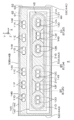
- FIG. 3 is a perspective view showing a semiconductor device 5 used as a 2-channel type transformer chip.
- FIG. 4 is a plan view of the semiconductor device 5 shown in FIG.
- FIG. 7 is a cross-sectional view taken along the line VIII-VIII shown in FIG.
- the semiconductor device 5 includes a rectangular parallelepiped semiconductor chip 41.
- the semiconductor chip 41 includes at least one of silicon, a wide bandgap semiconductor and a compound semiconductor.
- the wide bandgap semiconductor is composed of a semiconductor that exceeds the bandgap of silicon (about 1.12 eV). Wide bandgap The bandgap of the semiconductor is preferably 2.0 eV or more.
- the wide bandgap semiconductor may be SiC (silicon carbide).
- the compound semiconductor may be a group III-V compound semiconductor.
- the compound semiconductor may contain at least one of AlN (aluminum nitride), InN (indium nitride), GaN (gallium nitride) and GaAs (gallium arsenide).
- the semiconductor chip 41 includes a semiconductor substrate made of silicon.
- the semiconductor chip 41 may be an epitaxial substrate having a laminated structure including a silicon semiconductor substrate and a silicon epitaxial layer.
- the conductive type of the semiconductor substrate may be n-type or p-type.
- the epitaxial layer may be n-type or p-type.
- the semiconductor chip 41 has a first main surface 42 on one side, a second main surface 43 on the other side, and chip side walls 44A to 44D connecting the first main surface 42 and the second main surface 43.
- the first main surface 42 and the second main surface 43 are formed in a rectangular shape (rectangular shape in this form) in a plan view (hereinafter, simply referred to as “planar view”) viewed from their normal direction Z. ..
- the chip side walls 44A to 44D include a first chip side wall 44A, a second chip side wall 44B, a third chip side wall 44C, and a fourth chip side wall 44D.
- the first chip side wall 44A and the second chip side wall 44B form the long side of the semiconductor chip 41.
- the first chip side wall 44A and the second chip side wall 44B extend along the first direction X and face the second direction Y.
- the third chip side wall 44C and the fourth chip side wall 44D form the short side of the semiconductor chip 41.
- the third chip side wall 44C and the fourth chip side wall 44D extend in the second direction Y and face the first direction X.
- the chip side walls 44A to 44D are composed of a ground surface.
- the semiconductor device 5 further includes an insulating layer 51 formed on the first main surface 42 of the semiconductor chip 41.
- the insulating layer 51 has an insulating main surface 52 and insulating side walls 53A to 53D.
- the insulating main surface 52 is formed in a rectangular shape (rectangular shape in this form) that matches the first main surface 42 in a plan view.
- the insulating main surface 52 extends parallel to the first main surface 42.
- the insulating side walls 53A to 53D include a first insulating side wall 53A, a second insulating side wall 53B, a third insulating side wall 53C, and a fourth insulating side wall 53D.
- the insulating side walls 53A to 53D extend from the peripheral edge of the insulating main surface 52 toward the semiconductor chip 41 and are connected to the chip side walls 44A to 44D. Specifically, the insulating side walls 53A to 53D are formed flush with respect to the chip side walls 44A to 44D.
- the insulating side walls 53A to 53D form a flush grinding surface on the chip side walls 44A to 44D.
- the insulating layer 51 is composed of a multilayer insulating laminated structure including a lowermost insulating layer 55, an uppermost insulating layer 56, and a plurality of (11 layers in this form) interlayer insulating layers 57.
- the bottom insulating layer 55 is an insulating layer that directly covers the first main surface 42.
- the uppermost insulating layer 56 is an insulating layer forming the insulating main surface 52.
- the plurality of interlayer insulating layers 57 are insulating layers interposed between the lowermost insulating layer 55 and the uppermost insulating layer 56.
- the bottom insulating layer 55 in this form, has a single layer structure containing silicon oxide.
- the uppermost insulating layer 56 has a single-layer structure containing silicon oxide in this form.
- the thickness of the lowermost insulating layer 55 and the thickness of the uppermost insulating layer 56 may be 1 ⁇ m or more and 3 ⁇ m or less (for example, about 2 ⁇ m), respectively.
- the plurality of interlayer insulating layers 57 each have a laminated structure including a first insulating layer 58 on the lowermost insulating layer 55 side and a second insulating layer 59 on the uppermost insulating layer 56 side.
- the first insulating layer 58 may contain silicon nitride.
- the first insulating layer 58 is formed as an etching stopper layer for the second insulating layer 59.
- the thickness of the first insulating layer 58 may be 0.1 ⁇ m or more and 1 ⁇ m or less (for example, about 0.3 ⁇ m).
- the second insulating layer 59 is formed on the first insulating layer 58. It contains an insulating material different from that of the first insulating layer 58.
- the second insulating layer 59 may contain silicon oxide.
- the thickness of the second insulating layer 59 may be 1 ⁇ m or more and 3 ⁇ m or less (for example, about 2 ⁇ m). The thickness of the second insulating layer 59 preferably exceeds the thickness of the first insulating layer 58.
- the total thickness DT of the insulating layer 51 may be 5 ⁇ m or more and 50 ⁇ m or less.
- the total thickness DT of the insulating layer 51 and the number of layers of the interlayer insulating layer 57 are arbitrary and are adjusted according to the withstand voltage (dielectric breakdown resistance) to be realized.
- the insulating materials of the lowermost insulating layer 55, the uppermost insulating layer 56, and the interlayer insulating layer 57 are arbitrary and are not limited to a specific insulating material.
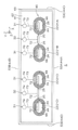
- the semiconductor device 5 includes a first functional device 45 formed on the insulating layer 51.
- the first functional device 45 includes one or more transformers 21 (corresponding to the transformers mentioned above). That is, the semiconductor device 5 is a multi-channel device including a plurality of transformers 21.
- the plurality of transformers 21 are formed in the inner portion of the insulating layer 51 at intervals from the insulating side walls 53A to 53D.
- the plurality of transformers 21 are formed at intervals in the first direction X.
- the plurality of transformers 21 are the first transformer 21A, the second transformer 21B, the third transformer 21C, and the first transformer 21A, the second transformer 21B, and the third transformer 21C formed in this order from the insulating side wall 53C side to the insulating side wall 53D side in a plan view.
- the plurality of transformers 21A to 21D each have a similar structure.
- the structure of the first transformer 21A will be described as an example.
- the description of the structure of the second transformer 21B, the third transformer 21C and the fourth transformer 21D the description of the structure of the first transformer 21A shall be applied mutatis mutandis and will be omitted.
- the first transformer 21A includes a low potential coil 22 and a high potential coil 23.
- the low potential coil 22 is formed in the insulating layer 51.
- the high-potential coil 23 is formed in the insulating layer 51 so as to face the low-potential coil 22 in the normal direction Z.
- the low-potential coil 22 and the high-potential coil 23 are formed in a region (that is, a plurality of interlayer insulating layers 57) sandwiched between the lowermost insulating layer 55 and the uppermost insulating layer 56.
- the low-potential coil 22 is formed in the insulating layer 51 on the lowermost insulating layer 55 (semiconductor chip 41) side, and the high-potential coil 23 has the uppermost insulating layer 56 in the insulating layer 51 with respect to the low-potential coil 22. It is formed on the (insulation main surface 52) side. That is, the high-potential coil 23 faces the semiconductor chip 41 with the low-potential coil 22 interposed therebetween.
- the location of the low-potential coil 22 and the high-potential coil 23 is arbitrary. Further, the high-potential coil 23 may face the low-potential coil 22 with one or more layers of the interlayer insulating layer 57 interposed therebetween.
- the distance between the low-potential coil 22 and the high-potential coil 23 (that is, the number of layers of the interlayer insulating layer 57) is appropriately adjusted according to the insulation withstand voltage and the electric field strength between the low-potential coil 22 and the high-potential coil 23.
- the low-potential coil 22 is formed in the interlayer insulating layer 57, which is the third layer counting from the lowermost insulating layer 55 side.
- the high potential coil 23 is formed on the interlayer insulating layer 57, which is the first layer counting from the uppermost insulating layer 56 side.
- the low-potential coil 22 is embedded in the interlayer insulating layer 57 so as to penetrate the first insulating layer 58 and the second insulating layer 59.
- the low potential coil 22 includes a first inner end 24, a first outer end 25, and a first spiral portion 26 spirally routed between the first inner end 24 and the first outer end 25.
- the first spiral portion 26 is drawn in a spiral shape extending in an elliptical shape (oval shape) in a plan view.
- the portion forming the innermost peripheral edge of the first spiral portion 26 defines the elliptical first inner region 66 in a plan view.
- the number of turns of the first spiral portion 26 may be 5 or more and 30 or less.
- the width of the first spiral portion 26 may be 0.1 ⁇ m or more and 5 ⁇ m or less.
- the width of the first spiral portion 26 is preferably 1 ⁇ m or more and 3 ⁇ m or less.
- the width of the first spiral portion 26 is defined by the width in the direction orthogonal to the spiral direction.
- the first winding pitch of the first spiral portion 26 may be 0.1 ⁇ m or more and 5 ⁇ m or less.
- the first winding pitch is preferably 1 ⁇ m or more and 3 ⁇ m or less.
- the first winding pitch is defined by the distance between two adjacent portions of the first spiral portion 26 in a direction orthogonal to the spiral direction.
- the winding shape of the first spiral portion 26 and the planar shape of the first inner region 66 are arbitrary and are not limited to the shapes shown in FIG. 5 and the like.
- the first spiral portion 26 may be wound into a polygonal shape such as a triangle shape or a quadrangular shape, or a circular shape in a plan view.
- the first inner region 66 may be divided into a polygonal shape such as a triangle shape, a quadrangular shape, or a circular shape in a plan view, depending on the winding shape of the first spiral portion 26.
- the low potential coil 22 may contain at least one of titanium, titanium nitride, copper, aluminum and tungsten.
- the low potential coil 22 may have a laminated structure including a barrier layer and a main body layer.
- the barrier layer partitions the recess space in the interlayer insulating layer 57.
- the barrier layer may contain at least one of titanium and titanium nitride.
- the body layer may contain at least one of copper, aluminum and tungsten.
- the high-potential coil 23 is embedded in the interlayer insulating layer 57 so as to penetrate the first insulating layer 58 and the second insulating layer 59.
- the high potential coil 23 includes a second inner end 27, a second outer end 28, and a second spiral portion 29 spirally routed between the second inner end 27 and the second outer end 28.
- the second spiral portion 29 is drawn in a spiral shape extending in an elliptical shape (oval shape) in a plan view.
- the portion forming the innermost peripheral edge of the second spiral portion 29, in this form partitions the second inner region 67 having an elliptical shape in a plan view.
- the second inner region 67 of the second spiral portion 29 faces the first inner region 66 of the first spiral portion 26 in the normal direction Z.
- the number of turns of the second spiral portion 29 may be 5 or more and 30 or less.
- the number of turns of the second spiral portion 29 with respect to the number of turns of the first spiral portion 26 is adjusted according to the voltage value to be boosted.
- the number of turns of the second spiral portion 29 preferably exceeds the number of turns of the first spiral portion 26.
- the number of turns of the second spiral portion 29 may be less than the number of turns of the first spiral portion 26, or may be equal to the number of turns of the first spiral portion 26.
- the width of the second spiral portion 29 may be 0.1 ⁇ m or more and 5 ⁇ m or less.
- the width of the second spiral portion 29 is preferably 1 ⁇ m or more and 3 ⁇ m or less.
- the width of the second spiral portion 29 is defined by the width in the direction orthogonal to the spiral direction.
- the width of the second spiral portion 29 is preferably equal to the width of the first spiral portion 26.
- the second winding pitch of the second spiral portion 29 may be 0.1 ⁇ m or more and 5 ⁇ m or less.
- the second winding pitch is preferably 1 ⁇ m or more and 3 ⁇ m or less.
- the second winding pitch is defined by the distance between two adjacent portions of the second spiral portion 29 in the direction orthogonal to the spiral direction.
- the second winding pitch is preferably equal to the first winding pitch of the first spiral portion 26.
- the winding shape of the second spiral portion 29 and the planar shape of the second inner region 67 are arbitrary and are not limited to the shapes shown in FIG. 6 and the like.
- the second spiral portion 29 may be wound into a polygonal shape such as a triangle shape or a quadrangular shape, or a circular shape in a plan view.
- the second inner region 67 may be divided into a polygonal shape such as a triangle shape, a quadrangular shape, or a circular shape in a plan view, depending on the winding shape of the second spiral portion 29.
- the high-potential coil 23 is preferably formed of the same conductive material as the low-potential coil 22. That is, the high-potential coil 23 preferably includes a barrier layer and a main body layer, similarly to the low-potential coil 22.
- the semiconductor device 5 includes a plurality of (12 in this figure) low-potential terminals 11 and a plurality of (12 in this figure) high-potential terminals 12.
- the plurality of low-potential terminals 11 are electrically connected to the low-potential coils 22 of the corresponding transformers 21A to 21D, respectively.
- the plurality of high-potential terminals 12 are electrically connected to the high-potential coils 23 of the corresponding transformers 21A to 21D, respectively.
- the plurality of low potential terminals 11 are formed on the insulating main surface 52 of the insulating layer 51. Specifically, the plurality of low potential terminals 11 are formed in the region on the insulating side wall 53B side at intervals in the second direction Y from the plurality of transformers 21A to 21D, and are arranged at intervals in the first direction X. Has been done.
- the plurality of low-potential terminals 11 include a first low-potential terminal 11A, a second low-potential terminal 11B, a third low-potential terminal 11C, a fourth low-potential terminal 11D, a fifth low-potential terminal 11E, and a sixth low-potential terminal 11F. include. In this embodiment, two low-potential terminals 11A to 11F are formed, respectively. The number of the plurality of low potential terminals 11A to 11F is arbitrary.
- the first low potential terminal 11A faces the first transformer 21A in the second direction Y in a plan view.
- the second low potential terminal 11B faces the second transformer 21B in the second direction Y in a plan view.
- the third low potential terminal 11C faces the third transformer 21C in the second direction Y in a plan view.
- the fourth low potential terminal 11D faces the fourth transformer 21D in the second direction Y in a plan view.
- the fifth low-potential terminal 11E is formed in a region between the first low-potential terminal 11A and the second low-potential terminal 11B in a plan view.
- the sixth low-potential terminal 11F is formed in a region between the third low-potential terminal 11C and the fourth low-potential terminal 11D in a plan view.
- the first low potential terminal 11A is electrically connected to the first inner terminal 24 of the first transformer 21A (low potential coil 22).
- the second low-potential terminal 11B is electrically connected to the first inner end 24 of the second transformer 21B (low-potential coil 22).
- the third low-potential terminal 11C is electrically connected to the first inner end 24 of the third transformer 21C (low-potential coil 22).
- the fourth low-potential terminal 11D is electrically connected to the first inner end 24 of the fourth transformer 21D (low-potential coil 22).
- the fifth low potential terminal 11E is electrically connected to the first outer end 25 of the first transformer 21A (low potential coil 22) and the first outer end 25 of the second transformer 21B (low potential coil 22). There is.
- the sixth low potential terminal 11F is electrically connected to the first outer end 25 of the third transformer 21C (low potential coil 22) and the first outer end 25 of the fourth transformer 21D (low potential coil 22). There is.
- the plurality of high-potential terminals 12 are formed on the insulating main surface 52 of the insulating layer 51 at intervals from the plurality of low-potential terminals 11. Specifically, the plurality of high-potential terminals 12 are formed in the region on the insulating side wall 53A side at intervals in the second direction Y from the plurality of low-potential terminals 11, and are arranged at intervals in the first direction X. ing.
- the plurality of high-potential terminals 12 are each formed in a region close to the corresponding transformers 21A to 21D in a plan view.
- the fact that the high-potential terminal 12 is close to the transformers 21A to 21D means that the distance between the high-potential terminal 12 and the transformer 21 is less than the distance between the low-potential terminal 11 and the high-potential terminal 12 in a plan view. means.
- the plurality of high potential terminals 12 are formed at intervals along the first direction X so as to face the plurality of transformers 21A to 21D along the first direction X in a plan view. .. More specifically, the plurality of high-potential terminals 12 are located along the first direction X so as to be located in a region between the second inner region 67 of the high-potential coil 23 and the adjacent high-potential coils 23 in a plan view. It is formed at intervals. As a result, the plurality of high-potential terminals 12 are arranged side by side with the plurality of transformers 21A to 21D in the first direction X in a plan view.
- the plurality of high-potential terminals 12 include a first high-potential terminal 12A, a second high-potential terminal 12B, a third high-potential terminal 12C, a fourth high-potential terminal 12D, a fifth high-potential terminal 12E, and a sixth high-potential terminal 12F. include. In this embodiment, two high-potential terminals 12A to 12F are formed, respectively. The number of the plurality of high potential terminals 12A to 12F is arbitrary.
- the first high-potential terminal 12A is formed in the second inner region 67 of the first transformer 21A (high-potential coil 23) in a plan view.
- the second high-potential terminal 12B is formed in the second inner region 67 of the second transformer 21B (high-potential coil 23) in a plan view.
- the third high-potential terminal 12C is formed in the second inner region 67 of the third transformer 21C (high-potential coil 23) in a plan view.
- the fourth high-potential terminal 12D is formed in the second inner region 67 of the fourth transformer 21D (high-potential coil 23) in a plan view.
- the fifth high potential terminal 12E is formed in the region between the first transformer 21A and the second transformer 21B in a plan view.
- the sixth high potential terminal 12F is formed in a region between the third transformer 21C and the fourth transformer 21D in a plan view.
- the first high potential terminal 12A is electrically connected to the second inner end 27 of the first transformer 21A (high potential coil 23).
- the second high-potential terminal 12B is electrically connected to the second inner end 27 of the second transformer 21B (high-potential coil 23).
- the third high-potential terminal 12C is electrically connected to the second inner end 27 of the third transformer 21C (high-potential coil 23).
- the fourth high potential terminal 12D is electrically connected to the second inner end 27 of the fourth transformer 21D (high potential coil 23).
- the fifth high potential terminal 12E is electrically connected to the second outer end 28 of the first transformer 21A (high potential coil 23) and the second outer end 28 of the second transformer 21B (high potential coil 23). There is.
- the sixth high potential terminal 12F is electrically connected to the second outer end 28 of the third transformer 21C (high potential coil 23) and the second outer end 28 of the fourth transformer 21D (high potential coil 23). There is.
- the semiconductor device 5 includes a first low-potential wiring 31, a second low-potential wiring 32, a first high-potential wiring 33, and a second high-potential wiring formed in the insulating layer 51, respectively. Including 34.
- a plurality of first low-potential wirings 31, a plurality of second low-potential wirings 32, a plurality of first high-potential wirings 33, and a plurality of second high-potential wirings 34 are formed.
- the first low-potential wiring 31 and the second low-potential wiring 32 fix the low-potential coil 22 of the first transformer 21A and the low-potential coil 22 of the second transformer 21B to the same potential. Further, in the first low-potential wiring 31 and the second low-potential wiring 32, the low-potential coil 22 of the third transformer 21C and the low-potential coil 22 of the fourth transformer 21D are fixed at the same potential. In this embodiment, the first low-potential wiring 31 and the second low-potential wiring 32 fix all the low-potential coils 22 of the transformers 21A to 21D to the same potential.
- the first high-potential wiring 33 and the second high-potential wiring 34 fix the high-potential coil 23 of the first transformer 21A and the high-potential coil 23 of the second transformer 21B to the same potential. Further, the first high-potential wiring 33 and the second high-potential wiring 34 fix the high-potential coil 23 of the third transformer 21C and the high-potential coil 23 of the fourth transformer 21D to the same potential. In this embodiment, the first high-potential wiring 33 and the second high-potential wiring 34 fix all the high-potential coils 23 of the transformers 21A to 21D to the same potential.
- the plurality of first low-potential wirings 31 are electrically connected to the first inner end 24 of the corresponding low-potential terminals 11A to 11D and the corresponding transformers 21A to 21D (low-potential coil 22), respectively.
- the plurality of first low-potential wirings 31 have a similar structure.
- the structure of the first low-potential wiring 31 connected to the first low-potential terminal 11A and the first transformer 21A will be described as an example.
- the description of the structure of the other first low-potential wiring 31 shall be applied mutatis mutandis and will be omitted.
- the first low-potential wiring 31 includes a through wiring 71, a low-potential connection wiring 72, a lead-out wiring 73, a first connection plug electrode 74, a second connection plug electrode 75, and one or more (plural) pad plug electrodes. 76 and one or more (s) substrate plug electrodes 77 in this form.
- the through wiring 71, the low potential connection wiring 72, the lead wiring 73, the first connection plug electrode 74, the second connection plug electrode 75, the pad plug electrode 76, and the substrate plug electrode 77 are made of the same conductive material as the low potential coil 22 and the like. It is preferable that each is formed. That is, the through wiring 71, the low potential connection wiring 72, the lead wiring 73, the first connection plug electrode 74, the second connection plug electrode 75, the pad plug electrode 76, and the substrate plug electrode 77 are the same as the low potential coil 22 and the like. It is preferable to include a barrier layer and a main body layer, respectively.
- the penetrating wiring 71 penetrates a plurality of interlayer insulating layers 57 in the insulating layer 51 and extends in a columnar shape extending along the normal direction Z.
- the through wiring 71 is formed in the region between the lowermost insulating layer 55 and the uppermost insulating layer 56 in the insulating layer 51.
- the through wiring 71 has an upper end portion on the uppermost insulating layer 56 side and a lower end portion on the lowermost insulating layer 55 side.
- the upper end of the through wiring 71 is formed in the same interlayer insulating layer 57 as the high potential coil 23, and is covered with the uppermost insulating layer 56.
- the lower end of the through wiring 71 is formed in the same interlayer insulating layer 57 as the low potential coil 22.
- the through wiring 71 includes a first electrode layer 78, a second electrode layer 79, and a plurality of wiring plug electrodes 80.
- the first electrode layer 78, the second electrode layer 79, and the wiring plug electrode 80 are each formed of the same conductive material as the low potential coil 22 and the like. That is, the first electrode layer 78, the second electrode layer 79, and the wiring plug electrode 80 include a barrier layer and a main body layer, respectively, like the low potential coil 22 and the like.
- the first electrode layer 78 forms the upper end portion of the through wiring 71.
- the second electrode layer 79 forms the lower end portion of the through wiring 71.
- the first electrode layer 78 is formed in an island shape and faces the low potential terminal 11 (first low potential terminal 11A) in the normal direction Z.
- the second electrode layer 79 is formed in an island shape and faces the first electrode layer 78 in the normal direction Z.
- the plurality of wiring plug electrodes 80 are embedded in the plurality of interlayer insulating layers 57 located in the region between the first electrode layer 78 and the second electrode layer 79, respectively.
- the plurality of wiring plug electrodes 80 are laminated from the lowest insulating layer 55 toward the uppermost insulating layer 56 so as to be electrically connected to each other, and the first electrode layer 78 and the second electrode layer 79 are electrically connected. You are connected.
- the plurality of wiring plug electrodes 80 each have a flat area of the first electrode layer 78 and a flat area less than the flat area of the second electrode layer 79.
- the number of layers of the plurality of wiring plug electrodes 80 matches the number of layers of the plurality of interlayer insulating layers 57.
- six wiring plug electrodes 80 are embedded in each interlayer insulating layer 57, but the number of wiring plug electrodes 80 embedded in each interlayer insulating layer 57 is arbitrary.
- one or a plurality of wiring plug electrodes 80 may be formed so as to penetrate the plurality of interlayer insulating layers 57.
- the low-potential connection wiring 72 is formed in the first inner region 66 of the first transformer 21A (low-potential coil 22) in the same interlayer insulating layer 57 as the low-potential coil 22.
- the low-potential connection wiring 72 is formed in an island shape and faces the high-potential terminal 12 (first high-potential terminal 12A) in the normal direction Z.
- the low-potential connection wiring 72 preferably has a flat area that exceeds the flat area of the wiring plug electrode 80.
- the low-potential connection wiring 72 is electrically connected to the first inner end 24 of the low-potential coil 22.
- the lead-out wiring 73 is formed in the region between the semiconductor chip 41 and the through wiring 71 in the interlayer insulating layer 57.
- the lead-out wiring 73 is formed in the interlayer insulating layer 57, which is the first layer counting from the lowest insulating layer 55.
- the lead-out wiring 73 includes a first end portion on one side, a second end portion on the other side, and a wiring portion connecting the first end portion and the second end portion.
- the first end of the lead-out wiring 73 is located in the region between the semiconductor chip 41 and the lower end of the through wiring 71.
- the second end of the lead wire 73 is located in the region between the semiconductor chip 41 and the low potential connection wire 72.
- the wiring portion extends along the first main surface 42 of the semiconductor chip 41, and extends in a band shape in the region between the first end portion and the second end portion.
- the first connection plug electrode 74 is formed in the region between the through wiring 71 and the lead wiring 73 in the interlayer insulating layer 57, and is electrically connected to the first end portion of the through wiring 71 and the lead wiring 73.
- the second connection plug electrode 75 is formed in the region between the low-potential connection wiring 72 and the lead-out wiring 73 in the interlayer insulating layer 57, and is electrically connected to the second end portion of the low-potential connection wiring 72 and the lead-out wiring 73. Has been done.
- the plurality of pad plug electrodes 76 are formed in the region between the low potential terminal 11 (first low potential terminal 11A) and the through wiring 71 in the uppermost insulating layer 56, and are formed at the upper ends of the low potential terminal 11 and the through wiring 71. Each is electrically connected.
- the plurality of substrate plug electrodes 77 are formed in the region between the semiconductor chip 41 and the lead-out wiring 73 in the lowermost insulating layer 55. In this embodiment, the substrate plug electrode 77 is formed in a region between the semiconductor chip 41 and the first end portion of the lead wire 73, and is electrically connected to the first end portion of the semiconductor chip 41 and the lead wire 73, respectively. There is.
- the plurality of first high-potential wirings 33 are located at the second inner ends 27 of the corresponding high-potential terminals 12A to 12D and the corresponding transformers 21A to 21D (high-potential coil 23), respectively. It is electrically connected.
- the plurality of first high-potential wirings 33 each have a similar structure.
- the structure of the first high-potential wiring 33 connected to the first high-potential terminal 12A and the first transformer 21A will be described as an example.
- the description of the structure of the other first high-potential wiring 33 the description of the structure of the first high-potential wiring 33 connected to the first transformer 21A shall be applied mutatis mutandis and will be omitted.
- the first high-potential wiring 33 includes a high-potential connection wiring 81 and one or more (plural in this form) pad plug electrodes 82.
- the high-potential connection wiring 81 and the pad plug electrode 82 are preferably formed of the same conductive material as the low-potential coil 22 and the like. That is, it is preferable that the high-potential connection wiring 81 and the pad plug electrode 82 include a barrier layer and a main body layer, similarly to the low-potential coil 22 and the like.
- the high-potential connection wiring 81 is formed in the second inner region 67 of the high-potential coil 23 in the same interlayer insulating layer 57 as the high-potential coil 23.
- the high-potential connection wiring 81 is formed in an island shape and faces the high-potential terminal 12 (first high-potential terminal 12A) in the normal direction Z.
- the high-potential connection wiring 81 is electrically connected to the second inner end 27 of the high-potential coil 23.
- the high-potential connection wiring 81 is formed at a distance from the low-potential connection wiring 72 in a plan view, and does not face the low-potential connection wiring 72 in the normal direction Z. As a result, the insulating distance between the low-potential connection wiring 72 and the high-potential connection wiring 81 is increased, and the withstand voltage of the insulating layer 51 is increased.
- the plurality of pad plug electrodes 82 are formed in the region between the high potential terminal 12 (first high potential terminal 12A) and the high potential connection wiring 81 in the uppermost insulating layer 56, and the high potential terminal 12 and the high potential connection wiring 81 are formed. Are electrically connected to each.
- the plurality of pad plug electrodes 82 each have a flat area smaller than the flat area of the high potential connection wiring 81 in a plan view.
- the distance D1 between the low-potential terminal 11 and the high-potential terminal 12 preferably exceeds the distance D2 between the low-potential coil 22 and the high-potential coil 23 (D2 ⁇ D1).
- the distance D1 preferably exceeds the total thickness DT of the plurality of interlayer insulating layers 57 (DT ⁇ D1).
- the ratio D2 / D1 of the distance D2 to the distance D1 may be 0.01 or more and 0.1 or less.
- the distance D1 is preferably 100 ⁇ m or more and 500 ⁇ m or less.
- the distance D2 may be 1 ⁇ m or more and 50 ⁇ m or less.
- the distance D2 is preferably 5 ⁇ m or more and 25 ⁇ m or less.
- the values of the distance D1 and the distance D2 are arbitrary and are appropriately adjusted according to the withstand voltage to be realized.
- the semiconductor device 5 includes a dummy pattern 85 embedded in the insulating layer 51 so as to be located around the transformers 21A to 21D in a plan view.
- the dummy pattern 85 is formed of a pattern (discontinuous pattern) different from that of the high-potential coil 23 and the low-potential coil 22, and is independent of the transformers 21A to 21D. That is, the dummy pattern 85 does not function as the transformers 21A to 21D.
- the dummy pattern 85 is formed as a shield conductor layer that shields the electric field between the low potential coil 22 and the high potential coil 23 in the transformers 21A to 21D and suppresses the electric field concentration on the high potential coil 23.
- the dummy pattern 85 is routed at a line density equal to the line density of the high potential coil 23 per unit area.
- the fact that the line density of the dummy pattern 85 is equal to the line density of the high potential coil 23 means that the line density of the dummy pattern 85 is within ⁇ 20% of the line density of the high potential coil 23.
- the depth position of the dummy pattern 85 inside the insulating layer 51 is arbitrary and is adjusted according to the electric field strength to be relaxed.
- the dummy pattern 85 is preferably formed in a region close to the high potential coil 23 with respect to the low potential coil 22 in the normal direction Z.
- the fact that the dummy pattern 85 is close to the high-potential coil 23 in the normal direction Z means that the distance between the dummy pattern 85 and the high-potential coil 23 is between the dummy pattern 85 and the low-potential coil 22 in the normal direction Z. Means less than the distance.
- the electric field concentration on the high potential coil 23 can be appropriately suppressed.
- the dummy pattern 85 is preferably formed in the same interlayer insulating layer 57 as the high potential coil 23. In this case, the electric field concentration on the high potential coil 23 can be suppressed more appropriately.
- the dummy pattern 85 includes a plurality of dummy patterns having different electrical states.
- the dummy pattern 85 may include a high potential dummy pattern.
- the depth position of the high potential dummy pattern 86 inside the insulating layer 51 is arbitrary, and is adjusted according to the electric field strength to be relaxed.
- the high-potential dummy pattern 86 is preferably formed in a region close to the high-potential coil 23 with respect to the low-potential coil 22 in the normal direction Z.
- the fact that the high-potential dummy pattern 86 is close to the high-potential coil 23 in the normal direction Z means that the distance between the high-potential dummy pattern 86 and the high-potential coil 23 in the normal direction Z is the high-potential dummy pattern 86 and the low-potential. It means that it is less than the distance between the coils 22.
- the dummy pattern 85 includes a floating dummy pattern formed in an electrically floating state in the insulating layer 51 so as to be located around the transformers 21A to 21D.
- the floating dummy pattern is drawn in a dense line shape so as to partially cover the area around the high potential coil 23 and partially expose it in a plan view.
- the floating dummy pattern may be formed in an endless shape or may be formed in an endless shape.
- the depth position of the floating dummy pattern inside the insulating layer 51 is arbitrary, and is adjusted according to the electric field strength to be relaxed.
- the number of floating lines is arbitrary and is adjusted according to the electric field to be relaxed.
- the floating dummy pattern may be composed of a plurality of floating.
- the semiconductor device 5 includes a second functional device 60 formed on the first main surface 42 of the semiconductor chip 41 in the device region 62.
- the second functional device 60 is formed by utilizing the surface layer portion of the first main surface 42 of the semiconductor chip 41 and / or the region above the first main surface 42 of the semiconductor chip 41, and is formed by utilizing the insulating layer 51 (bottom). It is covered with an insulating layer 55).
- the second functional device 60 is shown simplified by the broken line shown on the surface layer of the first main surface 42.
- the second function device 60 is electrically connected to the low potential terminal 11 via the low potential wiring and electrically connected to the high potential terminal 12 via the high potential wiring.
- the low-potential wiring has the same structure as the first low-potential wiring 31 (second low-potential wiring 32) except that the low-potential wiring is routed in the insulating layer 51 so as to be connected to the second functional device 60.
- the high-potential wiring has the same structure as the first high-potential wiring 33 (second high-potential wiring 34) except that the high-potential wiring is routed in the insulating layer 51 so as to be connected to the second functional device 60.
- Specific description of the low-potential wiring and the high-potential wiring according to the second function device 60 will be omitted.
- the second function device 60 may include at least one of a passive device, a semiconductor rectifying device and a semiconductor switching device.
- the passive device the second functional device 60 may include a network in which any two or more kinds of devices among passive devices, semiconductor rectifying devices and semiconductor switching devices are selectively combined.
- the network may form part or all of the integrated circuit.
- the passive device may include a semiconductor passive device. Passive devices may include resistances and / or capacitors.
- the semiconductor rectifying device may include at least one of a pn junction diode, a PIN diode, a Zener diode, a Schottky barrier diode and a fast recovery diode.
- the semiconductor switching device may include at least one of BJT [Bipolar Junction Transistor], MISFET [Metal Insulator Field Effect Transistor], IGBT [Insulated Gate Bipolar Junction Transistor], and JFET [Junction Field Effect Transistor].
- the semiconductor device 5 further includes a seal conductor 61 embedded in the insulating layer 51.
- the seal conductor 61 is embedded in the insulating layer 51 in a wall shape at intervals from the insulating side walls 53A to 53D in a plan view, and the insulating layer 51 is divided into a device region 62 and an outer region 63.
- the seal conductor 61 suppresses the ingress of moisture and the ingress of cracks from the outer region 63 into the device region 62.
- the device area 62 includes a first functional device 45 (a plurality of transformers 21), a second functional device 60, a plurality of low potential terminals 11, a plurality of high potential terminals 12, a first low potential wiring 31, and a second low potential wiring. 32, a region including a first high-potential wiring 33, a second high-potential wiring 34, and a dummy pattern 85.
- the outer region 63 is an region outside the device region 62.
- the seal conductor 61 is electrically separated from the device area 62.
- the seal conductor 61 includes a first functional device 45 (a plurality of transformers 21), a second functional device 60, a plurality of low potential terminals 11, a plurality of high potential terminals 12, and a first low potential wiring 31. It is electrically separated from the second low-potential wiring 32, the first high-potential wiring 33, the second high-potential wiring 34, and the dummy pattern 85. More specifically, the seal conductor 61 is electrically fixed in a floating state. The seal conductor 61 does not form a current path leading to the device region 62.
- the seal conductor 61 is formed in a strip shape along the insulating side walls 53 to 53D in a plan view.
- the seal conductor 61 is formed in a square annular shape (specifically, a rectangular annular shape) in a plan view.
- the seal conductor 61 partitions the device region 62 having a rectangular shape (specifically, a rectangular shape) in a plan view.
- the seal conductor 61 partitions the outer region 63 of the square ring (specifically, the rectangular ring) surrounding the device region 62 in a plan view.
- the seal conductor 61 has an upper end portion on the insulating main surface 52 side, a lower end portion on the semiconductor chip 41 side, and a wall portion extending like a wall between the upper end portion and the lower end portion.
- the upper end portion of the seal conductor 61 is formed at a distance from the insulating main surface 52 to the semiconductor chip 41 side, and is located in the insulating layer 51.
- the upper end of the seal conductor 61 is covered with the uppermost insulating layer 56 in this form.
- the upper end of the seal conductor 61 may be covered with one or more interlayer insulating layers 57.
- the upper end portion of the seal conductor 61 may be exposed from the uppermost insulating layer 56.
- the lower end portion of the seal conductor 61 is formed at a distance from the semiconductor chip 41 toward the upper end portion side.
- the seal conductor 61 is embedded in the insulating layer 51 so as to be located on the semiconductor chip 41 side with respect to the plurality of low-potential terminals 11 and the plurality of high-potential terminals 12. Further, in the insulating layer 51, the seal conductor 61 includes a first functional device 45 (a plurality of transformers 21), a first low potential wiring 31, a second low potential wiring 32, a first high potential wiring 33, and a second high potential. It faces the wiring 34 and the dummy pattern 85 in a direction parallel to the insulating main surface 52. The seal conductor 61 may face a part of the second functional device 60 in the insulating layer 51 in a direction parallel to the insulating main surface 52.
- the seal conductor 61 includes a plurality of seal plug conductors 64 and one or more (plural in this form) seal via conductor 65.
- the number of seal via conductors 65 is arbitrary.
- the uppermost seal plug conductor 64 among the plurality of seal plug conductors 64 forms the upper end portion of the seal conductor 61.
- Each of the plurality of seal via conductors 65 forms a lower end portion of the seal conductor 61.
- the seal plug conductor 64 and the seal via conductor 65 are made of the same conductive material as the low potential coil 22. That is, it is preferable that the seal plug conductor 64 and the seal via conductor 65 include a barrier layer and a main body layer as in the case of the low potential coil 22 and the like.
- the plurality of seal plug conductors 64 are each embedded in the plurality of interlayer insulating layers 57, and are formed in a square ring (specifically, a rectangular ring) surrounding the device region 62 in a plan view.
- the plurality of seal plug conductors 64 are laminated from the lowermost insulating layer 55 toward the uppermost insulating layer 56 so as to be connected to each other.
- the number of layers of the plurality of seal plug conductors 64 matches the number of layers of the plurality of interlayer insulating layers 57.
- one or more seal plug conductors 64 may be formed so as to penetrate the plurality of interlayer insulating layers 57.
- one annular seal conductor 61 is formed by an aggregate of a plurality of seal plug conductors 64, it is not necessary that all of the plurality of seal plug conductors 64 are formed in an annular shape.
- at least one of the plurality of seal plug conductors 64 may be formed in an endped shape.
- at least one of the plurality of seal plug conductors 64 may be divided into a plurality of endped strip-shaped portions.
- the plurality of seal plug conductors 64 are formed in an endless shape (annular shape).
- the plurality of seal via conductors 65 are each formed in the region between the semiconductor chip 41 and the seal plug conductor 64 in the lowermost insulating layer 55.
- the plurality of seal via conductors 65 are formed at intervals from the semiconductor chip 41 and are connected to the seal plug conductor 64.
- the plurality of seal via conductors 65 have a flat area smaller than the flat area of the seal plug conductor 64.
- the single seal via conductor 65 may have a flat area equal to or larger than the flat area of the seal plug conductor 64.
- the width of the seal conductor 61 may be 0.1 ⁇ m or more and 10 ⁇ m or less.
- the width of the seal conductor 61 is preferably 1 ⁇ m or more and 5 ⁇ m or less.
- the width of the seal conductor 61 is defined by the width in the direction orthogonal to the direction in which the seal conductor 61 extends.
- the semiconductor device 5 further includes a separation structure 130 that is interposed between the semiconductor chip 41 and the seal conductor 61 and electrically separates the seal conductor 61 from the semiconductor chip 41.
- the separation structure 130 preferably contains an insulator.
- the separation structure 130 is composed of a field insulating film 131 formed on the first main surface 42 of the semiconductor chip 41.
- the field insulating film 131 includes at least one of an oxide film (silicon oxide film) and a nitride film (silicon nitride film).
- the field insulating film 131 is preferably made of a LOCOS (local oxidation of silicon) film as an example of an oxide film formed by oxidation of the first main surface 42 of the semiconductor chip 41.
- the thickness of the field insulating film 131 is arbitrary as long as it can insulate the semiconductor chip 41 and the seal conductor 61.
- the thickness of the field insulating film 131 may be 0.1 ⁇ m or more and 5 ⁇ m or less.
- the separation structure 130 is formed on the first main surface 42 of the semiconductor chip 41 and extends in a strip shape along the seal conductor 61 in a plan view.
- the separated structure 130 is formed in a square ring (specifically, a rectangular ring) in a plan view.
- the separation structure 130 has a connection portion 132 to which the lower end portion (seal via conductor 65) of the seal conductor 61 is connected.
- the connecting portion 132 may form an anchor portion in which the lower end portion (seal via conductor 65) of the seal conductor 61 bites toward the semiconductor chip 41 side.
- the connecting portion 132 may be formed flush with respect to the main surface of the separation structure 130.
- the separation structure 130 includes an inner end portion 130A on the device region 62 side, an outer end portion 130B on the outer region 63 side, and a main body portion 130C between the inner end portion 130A and the outer end portion 130B.
- the inner end portion 130A partitions a region (that is, a device region 62) in which the second functional device 60 is formed in a plan view.
- the inner end portion 130A may be integrally formed with an insulating film (not shown) formed on the first main surface 42 of the semiconductor chip 41.
- the outer end portion 130B is exposed from the chip side walls 44A to 44D of the semiconductor chip 41 and is connected to the chip side walls 44A to 44D of the semiconductor chip 41. More specifically, the outer end portion 130B is formed flush with respect to the chip side walls 44A to 44D of the semiconductor chip 41. The outer end portion 130B forms a flush ground surface between the chip side walls 44A to 44D of the semiconductor chip 41 and the insulating side walls 53A to 53D of the insulating layer 51. Of course, in other forms, the outer end portion 130B may be formed in the first main surface 42 at a distance from the chip side walls 44A to 44D.
- the main body 130C has a flat surface extending substantially parallel to the first main surface 42 of the semiconductor chip 41.
- the main body portion 130C has a connecting portion 132 to which the lower end portion (seal via conductor 65) of the seal conductor 61 is connected.
- the connecting portion 132 is formed in a portion of the main body portion 130C at a distance from the inner end portion 130A and the outer end portion 130B.
- the separation structure 130 may take various forms other than the field insulating film 131.
- the semiconductor device 5 further includes an inorganic insulating layer 140 formed on the insulating main surface 52 of the insulating layer 51 so as to cover the seal conductor 61.
- the inorganic insulating layer 140 may be referred to as a passivation layer.
- the inorganic insulating layer 140 protects the insulating layer 51 and the semiconductor chip 41 from above the insulating main surface 52.
- the inorganic insulating layer 140 has a laminated structure including the first inorganic insulating layer 141 and the second inorganic insulating layer 142.
- the first inorganic insulating layer 141 may contain silicon oxide.
- the first inorganic insulating layer 141 preferably contains USG (undoped silicate glass), which is silicon oxide without impurities.
- the thickness of the first inorganic insulating layer 141 may be 50 nm or more and 5000 nm or less.
- the second inorganic insulating layer 142 may contain silicon nitride.
- the thickness of the second inorganic insulating layer 142 may be 500 nm or more and 5000 nm or less.
- the breakdown voltage (V / cm) of USG exceeds the breakdown voltage (V / cm) of silicon nitride. Therefore, when the inorganic insulating layer 140 is thickened, it is preferable that the first inorganic insulating layer 141, which is thicker than the second inorganic insulating layer 142, is formed.
- the first inorganic insulating layer 141 may contain at least one of BPSG (boron doped phosphor silicate glass) and PSG (phosphorus silicate glass) as an example of silicon oxide. However, in this case, since impurities (boron or phosphorus) are contained in the silicon oxide, it is particularly preferable to form the first inorganic insulating layer 141 made of USG in order to increase the withstand voltage on the high potential coil 23. ..
- the inorganic insulating layer 140 may have a single-layer structure composed of either the first inorganic insulating layer 141 or the second inorganic insulating layer 142.
- the inorganic insulating layer 140 covers the entire area of the seal conductor 61 and has a plurality of low-potential pad openings 143 and a plurality of high-potential pad openings 144 formed in a region outside the seal conductor 61.
- the plurality of low-potential pad openings 143 each expose the plurality of low-potential terminals 11.
- the plurality of high-potential pad openings 144 expose the plurality of high-potential terminals 12, respectively.
- the inorganic insulating layer 140 may have an overlapping portion that rides on the peripheral edge portion of the low potential terminal 11.
- the inorganic insulating layer 140 may have an overlapping portion that rides on the peripheral edge portion of the high potential terminal 12.
- the semiconductor device 5 further includes an organic insulating layer 145 formed on the inorganic insulating layer 140.
- the organic insulating layer 145 may contain a photosensitive resin.
- the organic insulating layer 145 may contain at least one of polyimide, polyamide and polybenzoxazole.
- the organic insulating layer 145 contains polyimide in this form.
- the thickness of the organic insulating layer 145 may be 1 ⁇ m or more and 50 ⁇ m or less.
- the thickness of the organic insulating layer 145 preferably exceeds the total thickness of the inorganic insulating layer 140. Further, the total thickness of the inorganic insulating layer 140 and the organic insulating layer 145 is preferably a distance D2 or more between the low potential coil 22 and the high potential coil 23. In this case, the total thickness of the inorganic insulating layer 140 is preferably 2 ⁇ m or more and 10 ⁇ m or less. Further, the thickness of the organic insulating layer 145 is preferably 5 ⁇ m or more and 50 ⁇ m or less.
- the thickness of the inorganic insulating layer 140 and the organic insulating layer 145 can be suppressed, and at the same time, the withstand voltage on the high potential coil 23 is appropriately increased by the laminated film of the inorganic insulating layer 140 and the organic insulating layer 145. be able to.
- the organic insulating layer 145 includes a first portion 146 that covers the region on the low potential side and a second portion 147 that covers the region on the high potential side.
- the first portion 146 covers the seal conductor 61 with the inorganic insulating layer 140 interposed therebetween.
- the first portion 146 has a plurality of low-potential terminal openings 148 that each expose a plurality of low-potential terminals 11 (low-potential pad openings 143) in a region outside the seal conductor 61.
- the first portion 146 may have an overlap portion that rides on the peripheral edge (overlap portion) of the low potential pad opening 143.
- the second portion 147 is formed at a distance from the first portion 146, and the inorganic insulating layer 140 is exposed from between the second portion 147 and the first portion 146.
- the second portion 147 has a plurality of high-potential terminal openings 149 each exposing the plurality of high-potential terminals 12 (high-potential pad openings 144).
- the second portion 147 may have an overlap portion that rides on the peripheral edge (overlap portion) of the high potential pad opening 144.
- the second part 147 collectively covers the transformers 21A to 21D and the dummy pattern 85. Specifically, the second portion 147 collectively covers a plurality of high-potential coils 23, a plurality of high-potential terminals 12, a first high-potential dummy pattern 87, a second high-potential dummy pattern 88, and a floating dummy pattern 121. are doing.
- the embodiment of the present invention can be implemented in still another embodiment.
- an example in which the first functional device 45 and the second functional device 60 are formed has been described.
- a form having only the second functional device 60 without having the first functional device 45 may be adopted.
- the dummy pattern 85 may be removed.
- the second functional device 60 can have the same effect as the effect described in the first embodiment (excluding the effect related to the dummy pattern 85).
- the second functional device 60 is formed.
- the second functional device 60 is not always necessary and may be removed.
- the dummy pattern 85 is formed.
- the dummy pattern 85 is not always necessary and may be removed.
- the first functional device 45 is a multi-channel type including a plurality of transformers 21 .
- a first functional device 45 consisting of a single channel type including a single transformer 21 may be adopted.
- FIG. 9 is a plan view (top view) schematically showing an example of the transformer arrangement in the 2-channel type transformer chip 300 (corresponding to the above-mentioned semiconductor device 5).
- the transformer chip 300 in this figure includes a first transformer 301, a second transformer 302, a third transformer 303, a fourth transformer 304, a first guard ring 305, a second guard ring 306, and pads a1 to a8. , Pads b1 to b8, pads c1 to c4, and pads d1 to d4.
- the pads a1 and b1 are connected to one end of the secondary coil L1s forming the first transformer 301, and the pads c1 and d1 are connected to the other end of the secondary coil L1s. ing.
- Pads a2 and b2 are connected to one end of the secondary coil L2s forming the second transformer 302, and pads c1 and d1 are connected to the other end of the secondary coil L2s.
- pads a3 and b3 are connected to one end of the secondary coil L3s forming the third transformer 303, and the pads c2 and d2 are connected to the other end of the secondary coil L3s.
- Pads a4 and b4 are connected to one end of the secondary coil L4s forming the fourth transformer 304, and pads c2 and d2 are connected to the other end of the secondary coil L4s.
- the primary side coil forming the first transformer 301, the primary side coil forming the second transformer 302, the primary side coil forming the third transformer 303, and the primary side coil forming the fourth transformer 304 will be any of them. Is not specified in this figure. However, each of the primary side coils basically has the same configuration as the secondary side coils L1s to L4s, and faces the secondary side coils L1s to L4s, respectively, and the secondary side coils L1s to L4s. It is located directly under each.
- the pads a5 and b5 are connected to one end of the primary coil forming the first transformer 301, and the pads c3 and d3 are connected to the other end of the primary coil. Further, the pads a6 and b6 are connected to one end of the primary coil forming the second transformer 302, and the pads c3 and d3 are connected to the other end of the primary coil.
- the pads a7 and b7 are connected to one end of the primary side coil forming the third transformer 303, and the pads c4 and d4 are connected to the other end of the primary side coil. Further, the pads a8 and b8 are connected to one end of the primary coil forming the fourth transformer 304, and the pads c4 and d4 are connected to the other end of the primary coil.
- pads a5 to a8, pads b5 to b8, pads c3 and c4, and pads d3 and d4 are pulled out from the inside to the surface of the trans chip 300 via vias (not shown).
- the pads a1 to a8 correspond to the first current supply pads
- the pads b1 to b8 correspond to the first voltage measurement pads, respectively.
- the pads c1 to c4 correspond to the second current supply pads, respectively
- the pads d1 to d4 correspond to the second voltage measurement pads, respectively.
- the series resistance component of each coil can be accurately measured at the time of inspecting the defective product. Therefore, it is necessary not only to reject defective products with broken wires in each coil, but also to appropriately reject defective products with abnormal resistance values of each coil (for example, halfway short circuit between coils). In the end, it is possible to prevent the outflow of defective products to the market.
- the plurality of pads may be used as connection means for connecting the primary side chip and the secondary side chip (for example, the controller chip 210 and the driver chip 220 described above). ..
- the pads a1 and b1, the pads a2 and b2, the pads a3 and b3, and the pads a4 and b4 may be connected to the signal input end or the signal output end of the secondary chip, respectively. Further, the pads c1 and d1 and the pads c2 and d2 may be connected to the common voltage application end (GND2) of the secondary chip, respectively.
- GND2 common voltage application end
- the pads a5 and b5, the pads a6 and b6, the pads a7 and b7, and the pads a8 and b8 may be connected to the signal input end or the signal output end of the primary chip, respectively. Further, the pads c3 and d3, and the pads c4 and d4 may be connected to the common voltage application end (GND1) of the primary chip, respectively.
- the first transformer 301 to the fourth transformer 304 are arranged by being coupled in each signal transmission direction.
- the first transformer 301 and the second transformer 302 that transmit a signal from the primary chip to the secondary chip are paired with the first guard ring 305.
- the third transformer 303 and the fourth transformer 304 that transmit a signal from the secondary chip to the primary chip are paired with the second guard ring 306.
- the reason for such coupling is that when the primary side coil and the secondary side coil forming the first transformer 301 to the fourth transformer 304 are stacked in the vertical direction of the substrate of the transformer chip 300, they are laminated and formed. This is to ensure a withstand voltage between the primary coil and the secondary coil.
- the first guard ring 305 and the second guard ring 306 are not necessarily essential components.
- the first guard ring 305 and the second guard ring 306 may be connected to low impedance wiring such as a grounding end via pads e1 and e2, respectively.
- the pads c1 and d1 are shared between the secondary coil L1s and the secondary coil L2s. Further, the pads c2 and d2 are shared between the secondary coil L3s and the secondary coil L4s. Further, the pads c3 and d3 are shared between the primary side coil L1p and the primary side coil L2p. Further, the pads c4 and d4 are shared with the corresponding primary coil. With such a configuration, it is possible to reduce the number of pads and reduce the size of the transformer chip 300.
- the primary side coil and the secondary side coil forming the first transformer 301 to the fourth transformer 304 respectively, have a rectangular shape (or a track with rounded corners) in the plan view of the transformer chip 300. It is desirable to wind it so that it becomes a shape). With such a configuration, the area of the portion where the primary side coil and the secondary side coil overlap each other becomes large, and it becomes possible to improve the transmission efficiency of the transformer.
- transformer arrangement in this figure is just an example, and the number, shape, arrangement, and pad arrangement of the coils are arbitrary. Further, the chip structure, transformer arrangement, and the like described so far can be applied to all semiconductor devices in which coils are integrated on a semiconductor chip.
- FIG. 10 is a diagram showing a basic configuration of a signal transmission device.
- the signal transmission device 400 of the present embodiment has the primary circuit system 400p to the secondary circuit system 400s while insulating between the primary circuit system 400p (Vcc1-GND1 system) and the secondary circuit system 400s (Vcc2-GND2 system). It is a semiconductor integrated circuit device (so-called insulated gate driver IC) that transmits a pulse signal to and drives a gate of a power transistor (not shown) provided in the secondary circuit system 400s.
- the signal transmission device 400 corresponds to the above-mentioned signal transmission device 200.
- the signal transduction device 400 has a plurality of external terminals (in this figure, a VCC1 pin, an IN pin, an MO pin, a GND1 pin, a VCS2 pin, an OUT pin, etc.) as means for establishing an electrical connection with the outside of the device.
- the MI pin and the GND2 pin are exemplified).
- the IN pin pulse signal input terminal
- the MO pin (monitor output terminal) is connected to a host device (ECU or the like) (not shown).
- the OUT pin (pulse signal output terminal) is connected to the gate of a power transistor (not shown).
- the MI pin (monitor input terminal) is connected to a signal source to be monitored (not shown).
- the signal transmission device 400 is used for all applications (motor drivers or DC / DC converters that handle high voltage, etc.) that require signal transmission between the primary circuit system 400p and the secondary circuit system 400s while insulating them from each other. ) Can be widely applied.
- the controller chip 410 is a semiconductor chip that integrates circuit elements of a primary circuit system 400p that operates by receiving a supply of a power supply voltage Vcc1 (for example, a maximum of 7V based on GND1).
- the driver chip 420 is a semiconductor chip in which circuit elements of the secondary circuit system 400s that operate by receiving a supply of a power supply voltage Vcc2 (for example, a maximum of 30V based on GND2) are integrated.
- the transformer chip 430 is a semiconductor chip in which a transformer for bidirectional signal transmission is integrated while insulating the controller chip 410 and the driver chip 420.
- the signal transmission device 400 of this configuration example independently has a transformer chip 430 on which only a transformer is mounted, in addition to the controller chip 410 and the driver chip 420, and these three chips are packaged in a single package. It is sealed in.
- both the controller chip 410 and the driver chip 420 can be formed by a general low withstand voltage to medium withstand voltage process (withstand voltage of several V to several tens of V), and thus are dedicated. It is not necessary to use a high withstand voltage process (withstand voltage of several kV), and the manufacturing cost can be reduced.
- controller chip 410 and the driver chip 420 can both be created by a proven existing process, and there is no need to perform a new reliability test, so the development period can be shortened and the development cost can be reduced. It can contribute to the reduction.
- the signal transmission device 400 includes an insulation signal transmission circuit 510 and an insulation monitoring circuit 520.
- the isolated signal transmission circuit 510 is connected from the primary circuit system 400p to the secondary circuit system 400p while insulating between the primary circuit system 400p and the secondary circuit system 400s via the insulating element ISO1 (transformer or the like) integrated in the transformer chip 430. A pulse signal is transmitted to the next circuit system 400s.
- the isolated signal transmission circuit 510 uses the input pulse signal S1 input to the IN pin of the primary circuit system 400p as the output pulse signal S2 output from the OUT pin of the secondary circuit system 400s. introduce.
- the insulation monitoring circuit 520 is a host device (ECU, etc.) while insulating the primary circuit system 400p and the secondary circuit system 400s via an insulating element ISO2 (transformer, etc.) integrated in the transformer chip 430.
- the parameters (voltage, temperature, etc.) of the secondary circuit system 400s that need to be detected are monitored, and the monitoring result is transmitted from the secondary circuit system 400s to the primary circuit system 400p.
- the insulation monitoring circuit 520 monitors the monitoring target signal S3 input to the MI pin of the secondary circuit system 400s, and the monitoring result pulse signal output from the MO pin of the primary circuit system 400p. It is transmitted as S4.
- the signal transmission device 400 has a built-in transformer chip 430 in which the insulating element ISO1 originally used for signal transmission from the primary circuit system 400p to the secondary circuit system 400s is integrated. Therefore, by additionally integrating the insulation element ISO2 for insulation monitoring on the above transformer chip 430, the monitoring result of the monitored signal S3 can be obtained from the secondary circuit system 400s to the primary circuit system 400p inside the signal transmission device 400. It becomes possible to transmit to.
- the circuit elements of the insulation signal transmission circuit 510 and the insulation monitoring circuit 520 are dispersed and integrated in the controller chip 410, the driver chip 420, and the transformer chip 430 (details will be described later).
- FIG. 11 is a diagram showing a configuration example of the isolated signal transmission circuit 510.
- the isolated signal transmission circuit 510 of this configuration example includes a Schmidt buffer 511, a pulse transmitting unit 512, a pulse receiving unit 513, a driver 514, and transformers 515 and 516 (corresponding to the above-mentioned insulating element ISO1). ..
- the Schmidt buffer 511 is an example of waveform shaping means, and is connected between the IN pin and the pulse transmission unit 512.
- the pulse transmission unit 512 pulse-drives either one of the transmission pulse signals S1a and S1b according to the logic level of the input pulse signal S1 input from the IN pin via the Schmidt buffer 511. For example, the pulse transmission unit 512 pulse drives (single or multiple transmission pulses) of the transmission pulse signal S1a applied to the primary winding 515p of the transformer 515 when notifying that the input pulse signal S1 is at a high level. Output) is performed to notify that the input pulse signal S1 is at a low level, and the transmission pulse signal S1b applied to the primary winding 516p of the transformer 516 is pulse-driven.
- the Schmidt buffer 511 and the pulse transmission unit 512 are both integrated in the controller chip 410 of the primary circuit system 400p (Vcc1-GND1 system).
- the pulse receiving unit 513 generates the received pulse signal S2c according to the received pulse signals S2a and S2b input from the transformers 515 and 516, respectively. For example, when the pulse receiving unit 513 receives the pulse drive of the transmitting pulse signal S1a and detects the induced pulse of the received pulse signal S2a appearing in the secondary winding 515s of the transformer 515, the pulse receiving unit 513 stands the received pulse signal S2c at a low level. Lower.
- the pulse receiving unit 513 when the pulse receiving unit 513 receives the pulse drive of the transmitting pulse signal S1b and detects the induced pulse of the received pulse signal S2b appearing in the secondary winding 516s of the transformer 516, the pulse receiving unit 513 stands the received pulse signal S2c at a high level. increase.
- the output pulse signal S2 becomes high level when the received pulse signal S2c is low level, and the output pulse signal S2 becomes low level when the received pulse signal S2c is high level.
- the logic level of the output pulse signal S2 is switched according to the logic level of the input pulse signal S1.
- Both the pulse receiving unit 513 and the driver 514 are integrated in the driver chip 420 of the secondary circuit system 400s (Vcc2-GND2 system).
- the transformer 515 outputs the received pulse signal S2a from the secondary winding 515s in response to the transmission pulse signal S1a input to the primary winding 515p.
- the transformer 516 outputs the received pulse signal S2b from the secondary winding 516s in response to the transmission pulse signal S1b input to the primary winding 516p.
- the above transformers 515 and 516 are both integrated in the transformer chip 430.
- the transformer chip 430 uses transformers 515 and 516 to insulate between the controller chip 410 and the driver chip 420, and uses the transmission pulse signals S1a and S1b input from the pulse transmission unit 512 as the reception pulse signals S2a and S2b, respectively. It is output to the pulse receiving unit 513.
- FIG. 12 is a diagram showing an example of an isolated signal transmission operation by the isolated signal transmission circuit 510, in order from the top, an input pulse signal S1, a transmission pulse signal S1a and S1b, a reception pulse signal S2a to S2c, and an output pulse signal. S2 is depicted. In this figure, the description of the signal delay is omitted for convenience of explanation.
- the pulse transmission unit 512 performs pulse drive of the transmission pulse signal S1a at the rising edge of the input pulse signal S1 at time t1, while pulse driving of the transmission pulse signal S1b at the falling edge of the input pulse signal S1 at time t2.
- the pulse receiving unit 513 detects the induced pulse of the received pulse signal S2a generated by the pulse drive of the transmitted pulse signal S1a and lowers the received pulse signal S2c to a low level, while the received pulse signal generated by the pulse drive of the transmitted pulse signal S1b.
- the induced pulse of S2b is detected and the received pulse signal S2c is raised to a high level.
- the output pulse signal S2 when the input pulse signal S1 rises to a high level, the output pulse signal S2 also rises to a high level, and conversely, when the input pulse signal S1 falls to a low level, the output pulse signal S2 rises accordingly. Also falls to the low level.
- FIG. 13 is a diagram showing a first embodiment of the insulation monitoring circuit 520.
- the insulation monitoring circuit 520 of the present embodiment includes a current source 521, a switch 522, a buffer 523, a pulse converter 524, a pulse transmission unit 525, a pulse reception unit 526, and transformers 527 and 528 (the above-mentioned insulation). (Equivalent to element ISO2) and.
- the current source 521 generates a source current to the MI pin.
- the switch 522 conducts / cuts off between the current source 521 and the MI pin. That is, when the switch 522 is on, the source current flows through the MI pin. On the other hand, when the switch 522 is off, the source current does not flow to the MI pin.
- the buffer 523 transmits the monitored signal S3 externally input to the MI pin to the pulse converter 524 in the subsequent stage.
- the pulse converter 524 generates a PWM [pulse width modulation] signal s10 having a duty corresponding to the signal value of the monitored signal S3 input via the buffer 523.
- a PWM [pulse width modulation] signal s10 having a duty corresponding to the signal value of the monitored signal S3 input via the buffer 523.
- the pulse transmission unit 525 pulse-drives either one of the transmission pulse signals s11a and s11b according to the logic level of the PWM signal s10. For example, the pulse transmission unit 525 pulse-drives (single or multiple transmission pulses) of the transmission pulse signal s11a applied to the secondary winding 527s of the transformer 527 when notifying that the PWM signal s10 is at a high level. Output) is performed to notify that the PWM signal s10 is at a low level, and the pulse drive of the transmission pulse signal s11b applied to the secondary winding 528s of the transformer 528 is performed.
- the current source 521, the switch 522, the buffer 523, the pulse converter 524, and the pulse transmission unit 525 are all integrated in the driver chip 420 of the secondary circuit system 400s (Vcc2-GND2 system).
- the pulse receiving unit 526 generates a monitoring result pulse signal S4 according to the received pulse signals s12a and s12b input from the transformers 527 and 528, respectively, and outputs the monitoring result pulse signal S4 from the MO pin to a host device (ECU or the like). For example, when the pulse receiving unit 526 receives the pulse drive of the transmitting pulse signal s11a and detects the induced pulse of the received pulse signal s12a appearing in the primary winding 527p of the transformer 527, the monitoring result pulse signal S4 stands at a high level. increase.
- the pulse receiving unit 526 receives the pulse drive of the transmitting pulse signal s11b and detects the induced pulse of the received pulse signal s12b appearing in the primary winding 528p of the transformer 528, the monitoring result pulse signal S4 stands at a low level. Lower. That is, the logic level of the monitoring result pulse signal S4 is switched according to the logic level of the PWM signal s10.
- the pulse receiving unit 526 is integrated in the controller chip 410 of the primary circuit system 400p (Vcc1-GND1 system).
- the transformer 527 outputs the received pulse signal s12a from the primary winding 527p in response to the transmission pulse signal s11a input to the secondary winding 527s.
- the transformer 528 outputs the received pulse signal s12b from the primary winding 528p in response to the transmission pulse signal s11b input to the secondary winding 528s.
- the above transformers 527 and 528 are both integrated in the transformer chip 430.
- the transformer chip 430 uses transformers 527 and 528 to insulate between the controller chip 410 and the driver chip 420, and uses the transmission pulse signals s11a and s11b input from the pulse transmission unit 525 as the reception pulse signals s12a and s12b, respectively. It is output to the pulse receiving unit 526.
- signal transmission device 400 provided with the insulation monitoring circuit 520 of the first embodiment is referred to as "signal transmission device GD1" in order to distinguish it from others.
- FIG. 14 is a diagram showing a configuration example (corresponding to a first application example) of an electronic device using the signal transmission device GD1.
- the electronic device A of this configuration example includes an upper gate driver IC1H (u / v / w), a lower gate driver IC1L (u / v / w), an upper power transistor 2H (u / v / w), and a lower part. It has a side power transistor 2L (u / v / w), an ECU 3, a motor 4, a resistance 5H (u / v / w), and a resistance 5L (u / v / w).
- the upper gate driver IC1H (u / v / w) and the lower gate driver IC1L (u / v / w) are both signal transmission devices GD1 provided with the insulation monitoring circuit 520 of the first embodiment. (FIG. 13) is used.
- the lower power transistor 2L (u / v / w) serves as a lower switch forming a three-phase (U-phase / V-phase / W-phase) half-bridge output stage, respectively, with each phase input end of the motor 4 and power. It is connected to the system grounding end.
- the upper power transistor 2H (u / v / w) and the lower power transistor 2L (u / v / w) each include a temperature sensor TaD (for example, a silicon diode) for detecting the ambient temperature Ta. .. Therefore, if it is necessary to obtain information on the ambient temperature Ta, a source current is passed through the temperature sensor TaD, and the temperature detection voltage V2 (u / v / w) (for example, the forward voltage drop of the silicon diode that fluctuates depending on the temperature). It suffices to read (corresponding to Vf).
- a temperature sensor TaD for example, a silicon diode
- N-channel MOSFETs metal oxide semiconductor field effect transistors
- a P-channel type MOSFET may be used as the upper power transistor 2H (u / v / w).
- IGBT insulated gate bipolar transistor
- the ECU 3 has an upper power transistor 2H (u / v / w) and a lower power transistor 2L (u) via the upper gate driver IC1H (u / v / w) and the lower gate driver IC1L (u / v / w).
- the rotational drive of the motor 4 is controlled.
- the ECU 3 has an overvoltage based on the monitoring results obtained by the insulation monitoring circuits 520 (not shown) of the upper gate driver IC1H (u / v / w) and the lower gate driver IC1L (u / v / w). It also has a function to perform protection operation and overheat protection operation.
- the motor 4 is a three-phase motor that is rotationally driven according to the three-phase drive voltage U / V / W input from each of the three-phase (U-phase / V-phase / W-phase) half-bridge output stages.
- the resistance 5H (u / v / w) and the resistance 5L (u / v / w) are connected in series between the power system power supply end and the power system grounding end, respectively, and are driven by a motor from the connection node of each phase.
- the voltage divider voltage V1 (u / v / w) corresponding to the voltage P VDD (for example, 48V to 700V) is output.
- the voltage dividing voltage V1 (u / v / w) is input to the upper gate driver IC1H (u / v / w), respectively.
- a temperature detection voltage V2 (u / v / w) is input to each of the lower gate driver IC1L (u / v / w). That is, the upper gate driver IC1H (u / v / w) is used to indirectly monitor the motor drive voltage P VDD, while the lower gate driver IC1L (u / v / w) is used to monitor the ambient temperature Ta.
- each insulation monitoring circuit 520 is used properly.
- FIG. 15 is a diagram showing only one phase of the first application example (FIG. 14) extracted.
- the output end of the pulse converter 524 is depicted as if it were directly connected to the MO pin, but in reality, the pulse transmitter 525 is located between the pulse converter 524 and the MO pin.
- a transformer 527 and a pulse receiving unit 526 are provided (see FIG. 13 above).
- the MI pin of the upper gate driver IC1H is a connection node between the resistors 5H and 5L. Therefore, the voltage dividing voltage V1 is input to the insulation monitoring circuit 520 as the monitoring target signal S3. At this time, since the switch 522 is turned off, the source current does not flow from the current source 521 to the MI pin.
- the MI pin of the lower gate driver IC 1L is connected to the temperature sensor TaD of the lower power transistor 2L.
- the switch 522 since the switch 522 is turned on, the source current flows from the current source 521 to the MI pin (and thus the temperature sensor TaD). Therefore, the temperature detection voltage V2 is input to the insulation monitoring circuit 520 as the monitoring target signal S3.
- the ECU 3 acquires information on the motor drive voltage P VDD based on the monitoring result pulse signal S4 input from the upper gate driver IC1H, while the monitoring result pulse input from the lower gate driver IC1L.
- Information about the ambient temperature Ta can be obtained based on the signal S4.
- the insulation monitoring circuit 520 is incorporated in all six signal transmission devices GD1.
- the specification to provide the insulation monitoring circuit 520 in all six signal transmission devices GD1 is wasteful and may be a factor of cost increase. ..
- the electronic device A of the first application example has six signal transmission devices GD1, and each signal transmission device GD1 has a voltage dividing voltage V1 (and thus a motor drive voltage P VDD) and a temperature detection voltage V2. Cannot be monitored at the same time. Therefore, in a system in which high quality is required for the voltage monitoring function and the temperature monitoring function by the ECU 3, there is a limitation in improving the robustness.
- FIG. 16 is a diagram showing a second embodiment of the insulation monitoring circuit 520.
- the switch 522 is removed, and the multiplexer 529 and the controller are removed, based on the first embodiment (FIG. 13) described above. 52A has been added. Further, the number of MI pins is increased from one to two (MI1 pin and MI2 pin). The current source 521 is connected to the MI2 pin.
- the multiplexer 529 selectively outputs one of the monitoring target signals S3a and S3b input to the MI1 pin and MI2 as the monitoring target signal S3 to the buffer 523, respectively.
- the MI pin may be one input. However, in that case, an external terminal for controlling the multiplexer is required separately. Also, the switch 522 cannot be omitted.
- the controller 52A controls the multiplexer 529 and the pulse converter 524 at predetermined timings so as to monitor the monitoring target signals S3a and S3b in a time-division manner.
- the controller 52A controls the multiplexer 529 so that the monitoring target signal S3a input to the MI1 pin is selectively output as the monitoring target signal S3 during the period T1 in which the monitoring target signal S3a should be monitored, and the monitoring target signal During the period T2 in which S3b should be monitored, the multiplexer 529 is controlled so that the monitoring target signal S3b input to the MI2 pin is selectively output as the monitoring target signal S3. Therefore, in the pulse converter 524, the signal values of the monitored signals S3a and S3b are time-divided into a single PWM signal s10 (further, the monitoring result pulse signal S4) (details will be described later).
- the pulse converter 524 is controlled so as to generate an identification pulse for informing the ECU 3 of the indication (details will be described later).
- the insulation monitoring circuit 520 is provided with a register for storing the signal values of the monitored signals S3a and S3b, and the CPU [central processing] such as I 2C [inter-integrated circuit] or UART [universal asynchronous receiver / transmitter].
- the monitoring result may be notified to the ECU 3 by using the unit] interface or the interface conforming to the communication standard for vehicles such as LIN [local interconnect network] and CAN [controller area network].
- FIG. 17 is a diagram showing a first example of time division control by the insulation monitoring circuit 520 of the second embodiment. As shown in this figure, the monitoring result pulse signal S4 alternately includes the header pulse HP and the data pulse DP.
- the data pulse DP corresponds to the PWM signal s10 having a duty corresponding to the signal value of the monitored signal S3a or S3b.
- a data pulse DP having a duty according to the voltage information) is output.
- the ECU 3 can acquire the temperature information of the secondary circuit system 400s from the monitoring result pulse signal S4 in the period T2.
- the signal values of the monitoring target signals S3a and S3b are used by using the single monitoring result pulse signal S4. Can be output to the ECU 3 in a time-division manner.
- FIG. 18 is a diagram showing a second example of time division control by the insulation monitoring circuit 520 of the second embodiment.
- the header pulse HP is not necessarily limited to high level fixed or low level fixed, and the data pulse DP following it indicates any signal value of the monitored signals S3a and S3b. It suffices if it can be uniquely identified.
- the header pulse HP may be set to low duty.
- the time division control of the second example is effective when the number of monitored signals is three or more.
- the footer pulse may be added after the data pulse DP to output in the frame format.
- the signal transmission device 400 provided with the insulation monitoring circuit 520 of the second embodiment will be referred to as “signal transmission device GD2" in order to distinguish it from others.
- the inexpensive signal transmission device 400 not provided with the insulation monitoring circuit 520 is referred to as “signal transmission device GD0" in order to distinguish it from others.
- FIG. 19 is a diagram showing an example of a configuration (corresponding to a second application example) of an electronic device using the signal transmission device GD2.
- the electronic device A of this configuration example is based on the first application example (FIG. 14) described above, and the signal transmission device GD2 (FIG. 16) is used as the lower gate driver IC1Lw, while the other upper gate driver IC1H. As (u / v / w) and the lower gate driver IC1L (u / v), an inexpensive signal transmission device GD0 is used.
- both the voltage dividing voltage V1w and the temperature detection voltage V2w are input to the lower gate driver IC1Lw. That is, the monitoring functions are integrated in the lower gate driver IC1Lw so that both the motor drive voltage P VDD and the ambient temperature Ta are time-division-monitored only by the lower gate driver IC1Lw.
- the other five gate driver ICs have been integrated into a single function for cost reduction.
- the signal transmission device GD2 does not necessarily have to be used as the lower gate driver IC1Lw of the W phase, and of the six upper gate driver IC1H (u / v / w) and the lower gate driver IC1L (u / v / w). One of them may be a signal transmission device GD2.
- FIG. 20 is a diagram showing only one phase of the second application example (FIG. 19) extracted.
- the output end of the pulse converter 524 is depicted as if it were directly connected to the MO pin, but in reality, the pulse transmitter 525 and the transformer are located between the pulse converter 524 and the MO pin.
- a 527 and a pulse receiving unit 526 are provided (see FIG. 16 above).
- the upper gate driver IC1H a signal transmission device GD0 having no insulation monitoring circuit 520 is used.
- the lower gate driver IC1L incorporates an insulation monitoring circuit 520 having a time division monitoring function.
- the MI1 pin of the lower gate driver IC1L is a connection node between the resistors 5H and 5L. Therefore, the voltage dividing voltage V1 is input to the insulation monitoring circuit 520 as the monitoring target signal S3a.
- the MI2 pin of the lower gate driver IC1L is connected to the temperature sensor TaD of the lower power transistor 2L. Since the current source 521 is connected to the MI2 pin, the source current flows from the current source 521 to the MI2 pin (and thus the temperature sensor TaD). Therefore, the temperature detection voltage V2 is input to the insulation monitoring circuit 520 as the monitoring target signal S3b.
- the controller 52A controls the multiplexer 529 and the pulse converter 524 at specified timings so as to monitor the monitoring target signals S3a and S3b in a time-division manner. Then, the monitoring results of the monitoring target signals S3a and S3b are transmitted from the lower gate driver IC1L to the ECU 3 in a time-division manner.
- the ECU 3 can acquire both the information regarding the motor drive voltage P whether and the information regarding the ambient temperature Ta based on the monitoring result pulse signal S4 input from the lower gate driver IC1L.
- FIG. 21 is a diagram showing another configuration example (corresponding to a third application example) of an electronic device using the signal transmission device GD2.
- the second application example (FIG. 19) described above is an example that emphasizes cost reduction, while the third application example emphasizes quality improvement (improvement of robustness) and six upper gate drivers IC1H (u / / Both v / w) and the lower gate driver IC1L (u / v / w) are referred to as a signal transmission device GD2.
- the ECU 3 is based on the monitoring result pulse signal S4 input from the upper gate driver IC1H (u / v / w) and the lower gate driver IC1L (u / v / w), respectively.
- Information on the motor drive voltage P VDD of the system and information on the ambient temperature Ta of the same system can be acquired.
- the quality improvement processing of each monitoring function (adoption of the majority voting method, calculation of the average value, or non-adoption of deviation values deviating from other signal values is adopted. Etc.) can be carried out. As a result, it becomes possible to improve the quality (improvement of robustness) of the voltage monitoring function and the temperature monitoring function by the ECU 3.
- the monitoring circuit capable of monitoring a plurality of monitored signals in a time-division manner can be applied not only to an isolated signal transmission device but also to a non-isolated signal transmission device.
- FIG. 22 is a diagram showing a configuration example of the pulse converter 524.
- the triangular wave oscillator 5241 generates a triangular wave-shaped or saw-shaped triangular wave signal TRI.
- the comparator 5242 compares the triangular wave signal TRI input to the non-inverting input end (+) with the monitored signal S3 input to the inverting input terminal (-), and generates a PWM signal s10.
- the PWM signal s10 has a high level when TRI> S3 and a low level when TRI ⁇ S3. Therefore, the higher the monitoring target signal S3, the lower the duty of the PWM signal s10, and the lower the monitoring target signal S3, the higher the duty of the PWM signal s10.
- the input polarity of the comparator 5242 may be opposite to that shown in this figure.
- As the drive voltage of the comparator 5242 it is desirable to use a constant voltage VREGH (bandgap voltage, regulator voltage, etc.) having little temperature dependence and power supply dependence.
- FIG. 23 is a diagram showing a configuration example of the triangular wave oscillator 5241.
- the triangular wave oscillator 5241 of this configuration example is a capacitor charge / discharge type oscillator, and includes a comparator CMP, a current source CS, a capacitor C1, an npn type bipolar transistor Q1, and resistors R1 to R4.
- the first end of each of the current source CS and the resistor R1 is connected to the power supply end.
- the second end of the current source CS and the first end of the capacitor C1 correspond to the application end of the charging voltage V11, and both are connected to the non-inverting input end (+) of the comparator CMP.
- the charging voltage V11 of the capacitor C1 is output as a triangular wave signal TRI.
- the second end of the resistance R1 and the first end of the resistance R2 correspond to the application end of the threshold voltage V12, and both are connected to the inverting input end ( ⁇ ) of the comparator CMP.
- the second end of each of the capacitor C1 and the resistor R2 is connected to the ground end.
- the resistance R2 may be a variable resistance whose resistance value can be adjusted.
- the current source CS generates the charging current Ic of the capacitor C1.
- the rising slope of the charging voltage V11 (and thus the triangular wave signal) becomes steeper as the charging current Ic is larger, and conversely becomes slower as the charging current Ic is smaller.
- the comparator CMP compares the charging voltage V11 input to the non-inverting input end (+) with the threshold voltage V12 input to the inverting input terminal (-) to generate a comparison signal Sc.
- the comparison signal Sc has a low level when V11 ⁇ V12 and a high level when V11> V12.
- the transistor Q1 functions as a discharge switch that discharges the capacitor C1 in response to the comparison signal Sc. According to this figure, the transistor Q1 is turned off when the comparison signal Sc is at a low level and turned on when the comparison signal Sc is at a high level.
- the comparison signal Sc becomes a low level, so that the transistor Q1 is turned off.
- the charging voltage V11 rises with an inclination corresponding to the charging current Ic.
- the comparison signal Sc becomes a high level, so that the transistor Q1 is turned on. As a result, the capacitor C1 is discharged, so that the charging voltage V11 drops sharply to 0V.
- a capacitor using a polysilicon layer as a conductor is inexpensive, but on the other hand, when a voltage is applied, the depletion layer expands and the capacitance value changes, so that the voltage dependence of the capacitance value is relatively large.
- the capacitor C1 is formed by connecting the first capacitor element C1A and the second capacitor element C1B in parallel so that nodes having different polarities are connected to each other.
- the negative electrode node of the first capacitor element C1A and the positive electrode node of the second capacitor element C1B are connected to the first wiring L1 (for example, the wiring connected to the application end of the charging voltage V11).
- the positive electrode node of the first capacitor element C1A and the negative electrode node of the second capacitor element C1B are connected to the second wiring L2 (for example, the wiring connected to the ground end).
- FIG. 24 is a diagram showing the voltage characteristics of the capacitor C1, in which the horizontal axis shows the voltage applied to the capacitor C1 and the vertical axis shows the change ratio of the capacitance value.
- the one-dot chain line and the two-dot chain line in this figure show the voltage characteristics of the first capacitor element C1A and the second capacitor element C1B, respectively.
- the volatility of the capacitance value with respect to the applied voltage is large (+ x% to ⁇ y%) in each of the first capacitor element C1A and the second capacitor element C1B alone.
- the first capacitor element C1A and the second capacitor element C1B are connected in parallel so that nodes having different polarities are connected to each other, so that the respective voltage characteristics are offset.
- the triangular wave signal TRI can be generated with high accuracy. Therefore, the monitored signal S3 is accurately converted into the PWM signal s10 and transmitted. Is possible.
- ⁇ Capacitor element layout> 25 and 26 are a plan view and a vertical cross section of Z1-Z2 showing an example of the element layout of the capacitor C1, respectively.
- the capacitor C1 is formed by connecting the first capacitor element C1A and the second capacitor element C1B in parallel so that nodes having different polarities are connected to each other.
- the first capacitor element C1A was formed on the first conductor A1 and the first conductor A1 on the insulating film ISF formed on the surface of the substrate SUB (including the one on which the epi layer or the like was formed).
- the first dielectric A2 and the second conductor A3 formed on the first dielectric A2 are laminated.
- the second conductor A3 has a smaller area than the first conductor A1 and the first dielectric A2, and has a part of each of the first conductor A1 and the first dielectric A2. It is laminated so that it overlaps. Therefore, the area of the second conductor A3 becomes the effective area of the first capacitor element C1A.
- the second capacitor element C1B also has basically the same structure as the first capacitor element C1A, and has a third conductor B1, a second dielectric B2 formed on the third conductor B1, and a second capacitor element B1. 2 It is formed by laminating a fourth conductor B3 formed on a dielectric B2.
- the fourth conductor B3 has a smaller area than the third conductor B1 and the second dielectric B2, and has a part of each of the third conductor B1 and the second dielectric B2. It is laminated so that it overlaps. Therefore, the area of the fourth conductor B3 becomes the effective area of the second capacitor element C1B.
- first dielectric A2 and the second dielectric B2 are not covered with the second conductor A3 and the fourth conductor B3 on the surfaces of the first conductor A1 and the third conductor B1, respectively. It is formed up to the area.
- Both the first conductor A1 and the third conductor B1 are polysilicon layers. Both the first dielectric A2 and the second dielectric B2 are silicon nitride layers. Both the second conductor A3 and the fourth conductor B3 are aluminum layers. However, each material is just an example.
- the second conductor A3 is connected to the first wiring L1 (for example, the wiring connected to the application end of the charging voltage V11) via a plurality of vias A4 formed on the surface thereof.
- the first conductor A1 has a region that is not covered by either the first dielectric A2 or the second conductor A3, and the second wiring L2 (2nd wiring L2 () via a plurality of vias A5 formed in the region. For example, it is connected to the wiring connected to the grounding end). That is, the second conductor A3 corresponds to the positive end of the first capacitor element C1A, and the first conductor A1 corresponds to the negative end of the first capacitor element C1A.
- the fourth conductor B3 is connected to the second wiring L2 via a plurality of vias B4 formed on the surface thereof.
- the third conductor B1 has a region not covered by either the second dielectric B2 or the fourth conductor B3, and is connected to the first wiring L1 via a plurality of vias B5 formed in the region. It is connected. That is, the third conductor B1 corresponds to the positive end of the second capacitor element C1B, and the fourth conductor B3 corresponds to the negative end of the second capacitor element C1B.
- the first capacitor element C1A and the second capacitor element C1B are arranged side by side in the vertical direction of the paper surface after their respective planar structures are flipped horizontally.
- a plurality of vias A5 and B4 conducting between B3 and the second wiring L2 can be linearly arranged in parallel with each other.
- the first wiring L1 and the second wiring L2 can be laid linearly to increase the degree of integration of the capacitor C1.
- FIG. 27 is a diagram showing the appearance of a vehicle on which an electronic device is mounted.
- the vehicle X10 of this configuration example is equipped with various electronic devices X11 to X18 that operate by receiving electric power from a battery (not shown).
- the mounting positions of the electronic devices X11 to X18 in this figure may differ from the actual mounting positions for convenience of illustration.
- the electronic device X11 is an engine control unit that performs control related to the engine (injection control, electronic throttle control, idling control, oxygen sensor heater control, auto cruise control, etc.).
- the electronic device X12 is a lamp control unit that controls turning on and off such as HID [high intensity discharged lamp] or DRL [daytime running lamp].
- the electronic device X13 is a transmission control unit that performs control related to the transmission.
- the electronic device X14 is a braking unit that performs control related to the motion of the vehicle X10 (ABS [anti-lock brake system] control, EPS [electric power steering] control, electronic suspension control, etc.).
- ABS anti-lock brake system
- EPS electric power steering
- electronic suspension control etc.
- the electronic device X15 is a security control unit that controls drive such as a door lock or a security alarm.
- the electronic device X16 is an electronic device incorporated in the vehicle X10 at the factory shipment stage as a standard equipment or a manufacturer's option such as a wiper, an electric door mirror, a power window, a damper (shock absorber), an electric sunroof, and an electric seat. Is.
- the electronic device X17 is an electronic device that is optionally mounted on the vehicle X10 as a user option such as an in-vehicle A / V [audio / visual] device, a car navigation system, and an ETC [electronic toll collection system].
- the electronic device X18 is an electronic device equipped with a high withstand voltage motor such as an in-vehicle blower, an oil pump, a water pump, and a battery cooling fan.
- a high withstand voltage motor such as an in-vehicle blower, an oil pump, a water pump, and a battery cooling fan.
- the electronic devices X11 to X18 can be understood as specific examples of the electronic device A described above. That is, the above-mentioned signal transmission devices 200 and 400 can be incorporated into any of the electronic devices X11 to X18.
- the signal transmission device disclosed in the present specification has a capacitor in which a first capacitor element and a second capacitor element are connected in parallel so that nodes having different polarities are connected to each other.
- the analog signal is converted into a pulse signal and transmitted (first configuration).
- the first capacitor element is on the first conductor, the first conductor formed on the first conductor, and the first dielectric.
- the second conductor is formed by laminating the formed second conductor, and the second conductor element is formed on the third conductor, the second conductor formed on the third conductor, and the second conductor.
- the formed fourth conductor is laminated, the second conductor and the third conductor are connected to the first wiring, and the first conductor and the fourth conductor are the first.
- the configuration may be connected to two wires (second configuration).
- the first dielectric and the second dielectric are the second conductors on the surfaces of the first conductor and the third conductor, respectively.
- a configuration (third configuration) may be used in which the body and the region not covered by the fourth conductor are formed.
- the second conductor a plurality of vias conducting between the third conductor and the first wiring, the first conductor, and the first conductor. 4.
- the plurality of vias conducting between the conductor and the second wiring may be arranged linearly in parallel with each other (fourth configuration).
- the first conductor and the third conductor may both be configured to be a polysilicon layer (fifth configuration).
- the pulse converter that converts the analog signal into the pulse signal includes a triangular wave oscillator that generates the triangular wave signal, the triangular wave signal, and the analog.
- a configuration may be configured including a first comparator that compares the signals and generates the pulse signal.
- the triangular wave oscillator compares the capacitor, the current source for generating the charging current of the capacitor, and the charging voltage and the threshold voltage of the capacitor to obtain a comparison signal.
- a second comparator to be generated and a discharge switch for discharging the capacitor in response to the comparison signal may be included, and the charging voltage may be output as the triangular wave signal (seventh configuration).
- the signal transmission device having any of the first to seventh configurations includes a signal transmission circuit that transmits an input pulse signal of the primary circuit system as an output pulse signal of the secondary circuit system via the first insulating element. It has a monitoring circuit that transmits the monitoring result of the monitoring target signal in the secondary circuit system from the secondary circuit system to the primary circuit system via the second insulating element, and the analog signal becomes the monitoring target signal.
- the pulse signal may be configured to correspond to the monitoring result of the monitored signal (eighth configuration).
- the signal transmission device having the eighth configuration includes a first chip in which the circuit elements of the primary circuit system are integrated, a second chip in which the circuit elements of the secondary circuit system are integrated, and the first chip.
- the insulating element and the third chip in which the second insulating element is integrated may be sealed in a single package (nineth configuration).
- the electronic device disclosed in the present specification includes a power transistor and a gate driver IC for driving the gate of the power transistor, and the gate driver IC is any one of the above 1st to 9th. It is said that it is a configuration (10th configuration) which is a signal transmission device having the configuration of.
- the vehicle disclosed in the present specification has a configuration (11th configuration) having an electronic device having the above-mentioned tenth configuration.
Landscapes
- Engineering & Computer Science (AREA)
- Power Engineering (AREA)
- Physics & Mathematics (AREA)
- Nonlinear Science (AREA)
- Manufacturing & Machinery (AREA)
- Microelectronics & Electronic Packaging (AREA)
- Semiconductor Integrated Circuits (AREA)
Priority Applications (4)
| Application Number | Priority Date | Filing Date | Title |
|---|---|---|---|
| CN202180069550.7A CN116325508A (zh) | 2020-10-28 | 2021-10-21 | 信号传输装置、电子设备、车辆 |
| US18/250,035 US12143100B2 (en) | 2020-10-28 | 2021-10-21 | Signal transmission device, electronic device, and vehicle |
| JP2022559064A JPWO2022091922A1 (https=) | 2020-10-28 | 2021-10-21 | |
| DE112021004682.9T DE112021004682T5 (de) | 2020-10-28 | 2021-10-21 | Signalübertragungsvorrichtung, elektronische vorrichtung und fahrzeug |
Applications Claiming Priority (2)
| Application Number | Priority Date | Filing Date | Title |
|---|---|---|---|
| JP2020-180323 | 2020-10-28 | ||
| JP2020180323 | 2020-10-28 |
Publications (1)
| Publication Number | Publication Date |
|---|---|
| WO2022091922A1 true WO2022091922A1 (ja) | 2022-05-05 |
Family
ID=81382370
Family Applications (1)
| Application Number | Title | Priority Date | Filing Date |
|---|---|---|---|
| PCT/JP2021/038884 Ceased WO2022091922A1 (ja) | 2020-10-28 | 2021-10-21 | 信号伝達装置、電子機器、車両 |
Country Status (5)
| Country | Link |
|---|---|
| US (1) | US12143100B2 (https=) |
| JP (1) | JPWO2022091922A1 (https=) |
| CN (1) | CN116325508A (https=) |
| DE (1) | DE112021004682T5 (https=) |
| WO (1) | WO2022091922A1 (https=) |
Cited By (2)
| Publication number | Priority date | Publication date | Assignee | Title |
|---|---|---|---|---|
| WO2023248622A1 (ja) * | 2022-06-24 | 2023-12-28 | ローム株式会社 | 受信回路、信号伝達装置 |
| US20240006344A1 (en) * | 2022-07-01 | 2024-01-04 | Renesas Electronics Corporation | Semiconductor device and method of manufacturing the same |
Families Citing this family (1)
| Publication number | Priority date | Publication date | Assignee | Title |
|---|---|---|---|---|
| DE112021003946B4 (de) * | 2020-09-24 | 2024-08-08 | Rohm Co., Ltd. | Signalübertragungsvorrichtung, elektronische Vorrichtung und Fahrzeug |
Citations (2)
| Publication number | Priority date | Publication date | Assignee | Title |
|---|---|---|---|---|
| JP2018011108A (ja) * | 2016-07-11 | 2018-01-18 | 三菱電機株式会社 | 信号伝達装置、および、電力スイッチング素子駆動装置 |
| JP2018082325A (ja) * | 2016-11-17 | 2018-05-24 | 株式会社ノーリツ | 三角波生成回路、並びに、ファンモータ電流検出装置 |
Family Cites Families (19)
| Publication number | Priority date | Publication date | Assignee | Title |
|---|---|---|---|---|
| US4918454A (en) * | 1988-10-13 | 1990-04-17 | Crystal Semiconductor Corporation | Compensated capacitors for switched capacitor input of an analog-to-digital converter |
| US6069050A (en) | 1997-10-20 | 2000-05-30 | Taiwan Semiconductor Manufacturing Company | Cross-coupled capacitors for improved voltage coefficient |
| JP3586638B2 (ja) * | 2000-11-13 | 2004-11-10 | シャープ株式会社 | 半導体容量装置 |
| EP1351389A1 (en) | 2002-04-02 | 2003-10-08 | Dialog Semiconductor GmbH | Method and circuit for compensating mosfet capacitance variations in integrated circuits |
| KR100480603B1 (ko) | 2002-07-19 | 2005-04-06 | 삼성전자주식회사 | 일정한 커패시턴스를 갖는 금속-절연체-금속 커패시터를 포함하는 반도체 소자 |
| JP2006319446A (ja) * | 2005-05-10 | 2006-11-24 | Toyota Industries Corp | 分周回路 |
| JP4528841B2 (ja) * | 2008-03-12 | 2010-08-25 | 日立オートモティブシステムズ株式会社 | 電力変換装置 |
| JP2010199490A (ja) * | 2009-02-27 | 2010-09-09 | Fuji Electric Systems Co Ltd | パワー半導体装置の温度測定装置およびこれを使用したパワー半導体モジュール |
| JP5375952B2 (ja) * | 2009-03-31 | 2013-12-25 | 日本電気株式会社 | 半導体装置 |
| WO2011036428A1 (en) | 2009-09-23 | 2011-03-31 | X-Fab Semiconductor Foundries Ag | Ultra-low voltage coefficient capacitors |
| CN102783005A (zh) * | 2009-12-28 | 2012-11-14 | 汤姆森特许公司 | 同步整流器禁用装置 |
| JP6104512B2 (ja) | 2011-04-01 | 2017-03-29 | ローム株式会社 | 温度検出装置 |
| WO2012177873A2 (en) | 2011-06-22 | 2012-12-27 | Arkansas Power Electronics International, Inc. | High temperature half bridge gate driver |
| JP5714455B2 (ja) | 2011-08-31 | 2015-05-07 | ルネサスエレクトロニクス株式会社 | 半導体集積回路 |
| JP5823235B2 (ja) * | 2011-09-30 | 2015-11-25 | 新電元工業株式会社 | スイッチング電源装置 |
| JP5977950B2 (ja) * | 2012-01-19 | 2016-08-24 | ローム株式会社 | Dc/dcコンバータおよびその制御回路、それを用いた電源装置、電源アダプタおよび電子機器 |
| US20170317529A1 (en) * | 2012-05-21 | 2017-11-02 | University Of Washington | Distributed control adaptive wireless power transfer system |
| JP5964183B2 (ja) | 2012-09-05 | 2016-08-03 | ルネサスエレクトロニクス株式会社 | 半導体装置 |
| US11811396B2 (en) * | 2021-09-30 | 2023-11-07 | Infineon Technologies Austria Ag | Power transfer, gate drive, and/or protection functions across an isolation barrier |
-
2021
- 2021-10-21 JP JP2022559064A patent/JPWO2022091922A1/ja active Pending
- 2021-10-21 CN CN202180069550.7A patent/CN116325508A/zh active Pending
- 2021-10-21 US US18/250,035 patent/US12143100B2/en active Active
- 2021-10-21 DE DE112021004682.9T patent/DE112021004682T5/de active Pending
- 2021-10-21 WO PCT/JP2021/038884 patent/WO2022091922A1/ja not_active Ceased
Patent Citations (2)
| Publication number | Priority date | Publication date | Assignee | Title |
|---|---|---|---|---|
| JP2018011108A (ja) * | 2016-07-11 | 2018-01-18 | 三菱電機株式会社 | 信号伝達装置、および、電力スイッチング素子駆動装置 |
| JP2018082325A (ja) * | 2016-11-17 | 2018-05-24 | 株式会社ノーリツ | 三角波生成回路、並びに、ファンモータ電流検出装置 |
Cited By (2)
| Publication number | Priority date | Publication date | Assignee | Title |
|---|---|---|---|---|
| WO2023248622A1 (ja) * | 2022-06-24 | 2023-12-28 | ローム株式会社 | 受信回路、信号伝達装置 |
| US20240006344A1 (en) * | 2022-07-01 | 2024-01-04 | Renesas Electronics Corporation | Semiconductor device and method of manufacturing the same |
Also Published As
| Publication number | Publication date |
|---|---|
| US12143100B2 (en) | 2024-11-12 |
| DE112021004682T5 (de) | 2023-07-20 |
| US20240007100A1 (en) | 2024-01-04 |
| CN116325508A (zh) | 2023-06-23 |
| JPWO2022091922A1 (https=) | 2022-05-05 |
Similar Documents
| Publication | Publication Date | Title |
|---|---|---|
| US12395167B2 (en) | Signal transmission device, electronic device and vehicle | |
| US12278482B2 (en) | Isolated gate driver, traction inverter, and electric vehicle | |
| WO2022091922A1 (ja) | 信号伝達装置、電子機器、車両 | |
| US12407242B2 (en) | Isolated gate driver, traction inverter, and electric vehicle | |
| US20250219875A1 (en) | Signal transmission device, electronic device, and vehicle | |
| US20250308770A1 (en) | Signal transmission device, electronic device and vehicle | |
| US20250309885A1 (en) | Power supply circuit, signal transmission device, electronic device and vehicle | |
| US20260081602A1 (en) | Power supply circuit, signal transmission device, electronic device, and vehicle | |
| US20260045946A1 (en) | Signal transmission device, electronic device and vehicle | |
| US12494782B2 (en) | Signal transmission device, electronic device, and vehicle | |
| US20260039301A1 (en) | Driving device, electronic device, and vehicle | |
| US20260031811A1 (en) | Signal transmission device and switching device | |
| US20240405772A1 (en) | Pulse transmission circuit, signal transmission device, electronic device, and vehicle | |
| US20260031806A1 (en) | Semiconductor device and switching device | |
| US20260004963A1 (en) | Signal transmission device, electronic device, and vehicle | |
| CN121794893A (zh) | 信号传递装置、电子设备、车辆 | |
| CN121889949A (zh) | 异常电压保护电路、具备该异常电压保护电路的信号传递装置、具备该信号传递装置的电子设备、以及具备该电子设备的车辆 | |
| WO2025062993A1 (ja) | 信号伝達装置および信号伝達装置を備えた電子機器、並びに電子機器を備えた車両 |
Legal Events
| Date | Code | Title | Description |
|---|---|---|---|
| 121 | Ep: the epo has been informed by wipo that ep was designated in this application |
Ref document number: 21886041 Country of ref document: EP Kind code of ref document: A1 |
|
| ENP | Entry into the national phase |
Ref document number: 2022559064 Country of ref document: JP Kind code of ref document: A |
|
| WWE | Wipo information: entry into national phase |
Ref document number: 18250035 Country of ref document: US |
|
| 122 | Ep: pct application non-entry in european phase |
Ref document number: 21886041 Country of ref document: EP Kind code of ref document: A1 |