WO2022064798A1 - 検査装置 - Google Patents
検査装置 Download PDFInfo
- Publication number
- WO2022064798A1 WO2022064798A1 PCT/JP2021/024153 JP2021024153W WO2022064798A1 WO 2022064798 A1 WO2022064798 A1 WO 2022064798A1 JP 2021024153 W JP2021024153 W JP 2021024153W WO 2022064798 A1 WO2022064798 A1 WO 2022064798A1
- Authority
- WO
- WIPO (PCT)
- Prior art keywords
- light
- optical amplifier
- optical
- photodetector
- input
- Prior art date
- Legal status (The legal status is an assumption and is not a legal conclusion. Google has not performed a legal analysis and makes no representation as to the accuracy of the status listed.)
- Ceased
Links
Images


Classifications
-
- G—PHYSICS
- G01—MEASURING; TESTING
- G01R—MEASURING ELECTRIC VARIABLES; MEASURING MAGNETIC VARIABLES
- G01R31/00—Arrangements for testing electric properties; Arrangements for locating electric faults; Arrangements for electrical testing characterised by what is being tested not provided for elsewhere
- G01R31/28—Testing of electronic circuits, e.g. by signal tracer
- G01R31/302—Contactless testing
- G01R31/308—Contactless testing using non-ionising electromagnetic radiation, e.g. optical radiation
- G01R31/311—Contactless testing using non-ionising electromagnetic radiation, e.g. optical radiation of integrated circuits
-
- G—PHYSICS
- G01—MEASURING; TESTING
- G01J—MEASUREMENT OF INTENSITY, VELOCITY, SPECTRAL CONTENT, POLARISATION, PHASE OR PULSE CHARACTERISTICS OF INFRARED, VISIBLE OR ULTRAVIOLET LIGHT; COLORIMETRY; RADIATION PYROMETRY
- G01J1/00—Photometry, e.g. photographic exposure meter
- G01J1/42—Photometry, e.g. photographic exposure meter using electric radiation detectors
-
- G—PHYSICS
- G01—MEASURING; TESTING
- G01R—MEASURING ELECTRIC VARIABLES; MEASURING MAGNETIC VARIABLES
- G01R31/00—Arrangements for testing electric properties; Arrangements for locating electric faults; Arrangements for electrical testing characterised by what is being tested not provided for elsewhere
- G01R31/28—Testing of electronic circuits, e.g. by signal tracer
- G01R31/317—Testing of digital circuits
- G01R31/31708—Analysis of signal quality
- G01R31/31709—Jitter measurements; Jitter generators
-
- H—ELECTRICITY
- H01—ELECTRIC ELEMENTS
- H01S—DEVICES USING THE PROCESS OF LIGHT AMPLIFICATION BY STIMULATED EMISSION OF RADIATION [LASER] TO AMPLIFY OR GENERATE LIGHT; DEVICES USING STIMULATED EMISSION OF ELECTROMAGNETIC RADIATION IN WAVE RANGES OTHER THAN OPTICAL
- H01S5/00—Semiconductor lasers
- H01S5/005—Optical components external to the laser cavity, specially adapted therefor, e.g. for homogenisation or merging of the beams or for manipulating laser pulses, e.g. pulse shaping
- H01S5/0085—Optical components external to the laser cavity, specially adapted therefor, e.g. for homogenisation or merging of the beams or for manipulating laser pulses, e.g. pulse shaping for modulating the output, i.e. the laser beam is modulated outside the laser cavity
-
- H—ELECTRICITY
- H10—SEMICONDUCTOR DEVICES; ELECTRIC SOLID-STATE DEVICES NOT OTHERWISE PROVIDED FOR
- H10F—INORGANIC SEMICONDUCTOR DEVICES SENSITIVE TO INFRARED RADIATION, LIGHT, ELECTROMAGNETIC RADIATION OF SHORTER WAVELENGTH OR CORPUSCULAR RADIATION
- H10F30/00—Individual radiation-sensitive semiconductor devices in which radiation controls the flow of current through the devices, e.g. photodetectors
- H10F30/20—Individual radiation-sensitive semiconductor devices in which radiation controls the flow of current through the devices, e.g. photodetectors the devices having potential barriers, e.g. phototransistors
- H10F30/21—Individual radiation-sensitive semiconductor devices in which radiation controls the flow of current through the devices, e.g. photodetectors the devices having potential barriers, e.g. phototransistors the devices being sensitive to infrared, visible or ultraviolet radiation
- H10F30/22—Individual radiation-sensitive semiconductor devices in which radiation controls the flow of current through the devices, e.g. photodetectors the devices having potential barriers, e.g. phototransistors the devices being sensitive to infrared, visible or ultraviolet radiation the devices having only one potential barrier, e.g. photodiodes
- H10F30/223—Individual radiation-sensitive semiconductor devices in which radiation controls the flow of current through the devices, e.g. photodetectors the devices having potential barriers, e.g. phototransistors the devices being sensitive to infrared, visible or ultraviolet radiation the devices having only one potential barrier, e.g. photodiodes the potential barrier being a PIN barrier
-
- H—ELECTRICITY
- H10—SEMICONDUCTOR DEVICES; ELECTRIC SOLID-STATE DEVICES NOT OTHERWISE PROVIDED FOR
- H10P—GENERIC PROCESSES OR APPARATUS FOR THE MANUFACTURE OR TREATMENT OF DEVICES COVERED BY CLASS H10
- H10P74/00—Testing or measuring during manufacture or treatment of wafers, substrates or devices
- H10P74/20—Testing or measuring during manufacture or treatment of wafers, substrates or devices characterised by the properties tested or measured, e.g. structural or electrical properties
- H10P74/203—Structural properties, e.g. testing or measuring thicknesses, line widths, warpage, bond strengths or physical defects
Definitions
- One aspect of the present invention relates to an inspection device.
- an inspection device capable of detecting a wide band phenomenon including a higher frequency band.
- an inspection device capable of accurately detecting a minute jigdah (for example, a jigdah of about 10 ps) in a transistor switching at a speed of less than 10 ps.
- One aspect of the present invention has been made in view of the above circumstances, and an object of the present invention is to provide an inspection device capable of accurately detecting a wideband phenomenon.
- the inspection device irradiates a semiconductor device with a light source that generates light, an optical amplifier that amplifies and outputs the input light, and light from the light source, and emits light from the semiconductor device. It includes an optical system that guides the light to the optical amplifier and an optical detector that detects the light output from the optical amplifier, and the optical amplifier amplifies the input light so as not to saturate it.
- light from a semiconductor device is input to an optical amplifier, the light is amplified and output within a range that does not saturate in the optical amplifier, and the light output from the optical amplifier is a photodetector.
- the amount of light emitted to a semiconductor device is reduced to such an extent that the semiconductor device is not destroyed. Therefore, the amount of return light from the semiconductor device is also small, but if the amount of return light is small, the detection accuracy may decrease due to the influence of noise (thermal noise) of the detection system. For this reason, conventionally, as a photodetector, a photodetector having a multiplying layer that amplifies the return light has been used.
- a photodetector having a multiplier layer has a relatively large capacitance, and is not suitable for high-speed signal measurement (detection of a phenomenon in a high frequency band).
- an optical amplifier is provided separately from the photodetector, and the light amplified by the photodetector is detected by the photodetector.
- the signal amplification for ensuring the detection accuracy is performed by an optical amplifier, and the light after amplification can be detected by a photodetector.
- a photodetector having a relatively small capacity without a multiplying layer can be used, so that a phenomenon in a high frequency band can be detected.
- light is amplified in a non-saturated range by an optical amplifier. When saturated, the minute signal contained in the input light disappears after amplification, and the minute signal may not be detected properly. In this respect, by amplifying the light in a non-saturating range, it is possible to accurately detect even a minute phenomenon based on the output light including a minute signal. As described above, according to the inspection apparatus according to one aspect of the present invention, it is possible to accurately detect a wideband phenomenon including a high frequency band.
- the optical amplifier may amplify the input light so that the change in the amount of output light with respect to the amount of input light is linear. As described above, the linear relationship between the input light and the output light makes it possible to accurately detect the phenomenon related to the return light from the semiconductor device.
- the optical amplifier may amplify the input light so that the amount of light to be output is larger than the amount of light that is half of the maximum amount of light that can be output. As a result, the amplification factor can be sufficiently increased while preventing saturation, and the detection accuracy of the phenomenon can be ensured.
- the optical amplifier may amplify the input light so that the shot noise contained in the output light exceeds the thermal noise of the photodetector. In this way, by amplifying the light so that the noise contained in the light becomes larger than the noise related to the photodetector, the noise contained in the light (shot noise and relative intensity noise) becomes dominant, and the light becomes dominant. It is possible to prevent the detection accuracy from deteriorating due to the influence of noise (thermal noise) related to the detector.
- the optical amplifier may have an amplification element having a length satisfying the condition of amplifying the input light so as not to saturate it. As a result, the input light can be appropriately amplified under the conditions set so as not to be saturated.
- the optical amplifier may be a semiconductor amplifier, an optical fiber optical amplifier, or a tapered amplifier. This makes it possible to appropriately amplify the light in the above-mentioned non-saturating range.
- the photodetector may be a PIN photodiode. As described above, by using a PIN photodiode having a relatively small capacity as a photodetector, it is possible to detect a phenomenon in a high frequency band.
- the photodetector may be configured to be capable of detecting light in the band of 8 GHz or higher. This makes it possible to detect a phenomenon in a high frequency band.
- an inspection device capable of accurately detecting a phenomenon in a wide band.
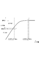
- FIG. 1 It is a block diagram of the inspection apparatus which concerns on embodiment of this invention. It is a block diagram of the optical measurement part included in the inspection apparatus of FIG. It is a figure which shows the input / output characteristic of an optical amplifier.
- the inspection device 1 is a semiconductor such as identifying an abnormality occurrence location in a semiconductor device D which is a measurement target and is a device to be inspected (DUT: Device Under Test). It is a device for inspecting the device D. More specifically, the inspection device 1 identifies the failure position by an optical probing technique called EOP or EOFM.
- the semiconductor device D includes an integrated circuit (IC: Integrated Circuit) having a PN junction such as a transistor, a logic device, a memory device, an analog device, which is a large-scale integrated circuit (LSI: Large Scale Integration), and a combination thereof. It may be a mixed signal device, or a power semiconductor device (power device) such as a high current / high pressure MOS transistor, a bipolar transistor, or an IGBT.
- the inspection device 1 includes a tester head 2, a test board 3, a stage 5, an objective lens 6, a turret 7, an imaging optical system 8, a scan optical system 9, a scan unit 11, and an optical measurement unit 12.
- a digitizing unit 13, a control device 14, and an input / output device 15 are provided.
- the stage 5, the objective lens 6, the turret 7, the imaging optical system 8, and the scanning optical system 9 are housed in the dark box 4.
- the stage 5 is a table that holds each configuration housed in the dark box 4.
- the tester head 2 mounts the semiconductor device D via the test board 3 and repeatedly applies a predetermined operation pulse signal to the semiconductor device D.
- the semiconductor device D is driven by the test signal.
- the tester head 2 has, for example, a pulse generator that generates an operation pulse signal for driving the semiconductor device D, a tester unit that inputs the operation pulse signal to the semiconductor device D, and a power supply.
- the test board 3 is a semiconductor substrate on which the semiconductor device D is mounted.
- the test board 3 has peripheral chips, circuits, terminals, and the like necessary for the operation of the semiconductor device D.
- the scan optical system 9 receives the light emitted from the light source 121 (see FIG. 2) of the optical measurement unit 12 via the optical fiber 10 and guides the light to the imaging optical system 8. Specifically, the light from the light source 121 passes through the optical coupler 122 (see FIG. 2) and is guided to the scan optical system 9 by the optical fiber 10.
- the fiber end of the optical fiber 10 may be, for example, an APC type in order to reduce reflected light.
- the scan optical system 9 has, for example, an optical scanner including an optical scanning element such as a galvano mirror or a MEMS (microelectromechanical system) mirror.
- the scanning optical system 9 irradiates (scans) the selected region on the semiconductor device D with the light emitted from the light source 121 of the optical measuring unit 12.
- the selected area is a spot or area selected by the user.
- the scan unit 11 controls the scan optical system 9 so that the spot in the selected region is irradiated with light based on the control by the control device 14.
- the imaging optical system 8 receives the light emitted from the light source 121 of the optical measurement unit 12 via the scan optical system 9 and guides the light to the objective lens 6.
- the objective lens 6 is a lens that collects the light from the light source 121 of the light measuring unit 12 onto the semiconductor device D.
- the objective lens 6 is configured to be switchable between a low magnification objective lens (for example, 5 times) and a high magnification objective lens (for example, 50 times) by a turret 7.
- the reflected light (return light) from the semiconductor device D is input to the optical measurement unit 12 via the objective lens 6, the imaging optical system 8, the scan optical system 9, and the optical fiber 10.
- the objective lens 6, the imaging optical system 8, and the scan optical system 9 irradiate the semiconductor device D with the light from the light source 121 of the optical measurement unit 12, and the reflected light (return light) from the semiconductor device D.
- the optical measurement unit 12 includes a light source 121, an optical coupler 122, an optical amplifier 123, a photodetector 124, and a high frequency amplifier 125.
- the light source 121 is operated by a power source (not shown) to generate and output light emitted to the semiconductor device D.
- the light may be coherent light or incoherent light.
- an SLD Super Luminescent Diode
- an ASE Ampton
- LED Light Emitting Diode
- the light output from the light source 121 is guided to the scan optical system 9 via the optical coupler 122 and the optical fiber 10.
- the optical coupler 122 is a PBS (Polarizing Beam Splitter) type optical coupler or a circulator type optical coupler.
- a ⁇ / 4 wave plate may be provided inside the scan optical system 9.
- a ⁇ / 2 wave plate may be provided inside the scan optical system 9.
- an optical splitter may be used instead for the optical coupler 122.
- a Faraday rotator may be provided inside the scan optical system 9 instead of the above-mentioned wave plate.
- the optical amplifier 123 receives the reflected light (return light) from the semiconductor device D via the optical fiber 10 and the optical coupler 122, amplifies the intensity of the reflected light (input light), and outputs the amplified light. ..
- the optical amplifier 123 is, for example, a semiconductor amplifier, an optical fiber amplifier (optical fiber optical amplifier), an SOA (Solid Optical Amplifier), a taper amplifier (taper type amplifier), a booster optical amplifier, or the like. Further, the optical amplifier 123 may be an amplifier using a crystal, gas, liquid or the like as a laser medium.
- the output light output by the optical amplifier 123 is input to the photodetector 124 via the optical fiber 10.
- FIG. 3 is a diagram showing the input / output characteristics of the optical amplifier 123.
- the horizontal axis shows the amount of input light to the optical amplifier 123
- the vertical axis shows the amount of output light from the optical amplifier 123.
- the gain of the optical amplifier 123 has a specific value determined for each wavelength according to the characteristics of the element (optical amplifier). Further, the upper limit of the intensity of light that can be output from the optical amplifier 123 is also determined. Therefore, when the intensity of the input input light becomes higher than a certain value, the optical amplifier 123 suppresses the optical amplification and cannot amplify the light according to the predetermined gain.
- the optical amplification characteristic of the optical amplifier 123 becomes non-linear.
- the state in which the optical amplification characteristic of the optical amplifier 123 is non-linear is the state in which the gain of the optical amplifier 123 is saturated.
- the gain saturation of the optical amplifier 123 at a certain wavelength means that all the charges that can contribute to the amplification of light at the certain wavelength are used up and the optical amplification is suppressed.
- the input light 1 in FIG. 3 is light having an intensity that does not saturate the optical amplifier 123.
- the input light 2 in FIG. 3 is light having an intensity at which the optical amplifier 123 is saturated.
- the optical amplification characteristic of the optical amplifier 123 becomes linear, and the input light 1 is linearly amplified.
- the minute signal included in the input light 1 (the portion where the range of "amplitude" is shown in FIG. 3) is also linearly amplified. Since the output light in this case includes ASE light (spontaneous emission light), noise increases a little.
- the optical amplifier 123 becomes gain saturated, so that the optical amplification characteristics of the optical amplifier 123 become non-linear, and the input light 2 reaches the output limit of the optical amplifier 123. It is output.
- the minute signal (small fluctuation) contained in the input light 2 is compressed and disappears.
- the amplification factor of the optical amplifier depends on the excited electron density and the length of the optical amplifier. Since the electrons in the ground state absorb light, the excited electron density described above is specifically the density of the electrons in the excited state minus the density of the electrons in the ground state. The longer the length of the optical amplifier, the more times the excited electrons and photons collide with each other, and the larger the amplification factor.
- Saturation of the optical amplifier means that as a result of the electrons in the excited state being used for amplification, the density of the electrons in the excited state becomes lower than the density of the electrons in the ground state near the outlet of the optical amplifier.
- the maximum output of amplified light depends on the excited electronic density, the intensity of the excited light in the case of an optical fiber amplifier, and the intensity of the supplied current (excitation current) in the case of SOA.
- the density of excited electrons can be increased and the amplification factor can be increased by increasing the excitation light or the excitation current.
- the maximum output increases at the same time as the density of excited electrons. That is, when the density of excited electrons is changed and the amplification factor is changed by changing the excitation light or the like, the maximum output also changes at the same time. Therefore, the saturated / unsaturated state of the light cannot be appropriately switched only by changing the excitation light or the like. Therefore, in order not to saturate the output light, an amplification element having an appropriate gain with respect to the input light, that is, an amplification element having an appropriate amplification length may be used. It should be noted that the output light can be configured not to be saturated by attenuating the input light, but since the S / N is deteriorated, even if the amplification length of the amplification element is appropriately designed as described above. good.
- noise floor when the input light is amplified so as not to be saturated, minute noise is superimposed on the amplified output light. This is called a noise floor, and although it depends on the amplification method, it is, for example, about 5 to 10 dB.
- the gain of the optical amplifier 123 is at least higher than this.
- the optical amplifier 123 amplifies the input reflected light so as not to saturate it. That is, the optical amplifier 123 amplifies the reflected light in a range in which the optical amplifier 123 does not saturate and the photodetector does not saturate.
- the optical amplifier 123 amplifies the input light so that the change in the amount of output light with respect to the amount of input reflected light is linear. For example, the optical amplifier 123 may amplify the input light so that the amount of output light is larger than half of the maximum amount of light that can be output. Further, for example, the optical amplifier 123 may amplify the input light so that the shot noise contained in the output light exceeds the thermal noise of the photodetector 124.
- the optical amplifier 123 has an amplification element having a length satisfying the condition of amplifying the input light so as not to saturate it as described above.
- the photodetector 124 is an optical sensor that detects the light output from the optical amplifier 123.
- the photodetector 124 is an optical sensor that detects a high-speed optical signal, and is, for example, an optical sensor configured to be able to detect light in a band of 8 GHz or higher.
- the photodetector 124 is, for example, a PIN photodiode.
- an optical sensor for example, a PIN photodiode
- the input is a single-mode fiber. Therefore, the optical fiber 10 for incident and the optical coupler 122 are all composed of a combination of single-mode fibers.
- the photodetector 124 may be, for example, an avalanche photodiode, a photomultiplier tube, an area image sensor, or the like configured to be capable of detecting a wide band signal of 8 GHz or more.
- the photodetector 124 outputs a detection signal (electrical signal).
- the detection signal output by the photodetector 124 is input to the high frequency amplifier 125 by the high frequency cable 16.
- the high frequency amplifier 125 amplifies the detection signal input from the photodetector 124 and outputs it as an amplified signal.
- the digitizing unit 13 waveforms and outputs the amplified signal input from the high frequency amplifier 125.
- the digitizing unit 13 is composed of, for example, a digitizer, an oscilloscope, an FPGA, or the like.
- the waveformized signal output by the digitizing unit 13 is input to the control device 14.
- the control device 14 is a device that controls the scan unit 11 and the digitizing unit 13.
- the control device 14 generates a waveform (analyzed image) based on the waveformized signal acquired from the digitizing unit 13, and inputs the analyzed image to the input / output device 15.
- the input / output device 15 has an input device such as a keyboard and a mouse into which measurement conditions and the like are input from the user, and a display device such as a monitor for showing the measurement result and the like to the user.
- the input / output device 15 displays the analysis image input from the control device 14. From the analysis image, it is possible to measure the Jeddah, check the switching image (waveform), and identify the faulty part.
- the light reflectance of an active device on a semiconductor device such as an LSI, for example, a transistor is about 10% or less, which is not large.
- the device such as a transistor may be destroyed by the incident light. Therefore, the amount of light emitted to the semiconductor device is reduced to such an extent that the semiconductor device is not destroyed.
- the upper limit of the amount of irradiated light is several mW, and the upper limit of the reflected light (return light) in that case is about 0.1 mW. ..
- the shot noise of light may be larger than the thermal noise of a measuring instrument (specifically, a photodetector or the like).
- the inspection device general inspection device
- the inspection device has a multiplier layer that amplifies the return light in order to make the shot noise larger than the thermal noise in a configuration in which the amount of return light is small as described above.
- a photodetector for example, a photodetector such as APD
- shot noise can be made larger than thermal noise, and highly accurate inspection can be performed.
- an inspection device capable of detecting a wide band phenomenon including a higher frequency band.
- an inspection device capable of accurately detecting a minute Jeddah (for example, a Jeddah of about 10 ps).
- the capacity of the photodetector is relatively large, so that high-speed signal detection (detection of a phenomenon in a high frequency band) cannot be performed.
- the photodetector for example, APD
- the photodetector has a multiplying layer between the P layer and the N layer, and a strong electric field is applied to the multiplying layer.
- a photodetector having a multiplier layer to which a strong electric field is applied its capacitance becomes relatively large, and high-speed signal detection (detection of a phenomenon in a high frequency band) cannot be performed.
- the inspection device 1 has a light source 121 that generates light, an optical amplifier 123 that amplifies and outputs the input light, and a semiconductor that outputs light from the light source 121.
- the optical system objective lens 6, imaging optical system 8, and scan optical system 9) that irradiates the device D and guides the light from the semiconductor device D to the optical amplifier 123, and the light output from the optical amplifier 123.
- the optical amplifier 123 includes an optical detector 124 for detecting the light, and the optical amplifier 123 amplifies the input light so as not to saturate it.
- an optical amplifier 123 is provided separately from the photodetector 124, and the light amplified by the photodetector 123 is detected by the photodetector 124, so that the detection accuracy is guaranteed.
- the amplification of the signal for this purpose is performed by the optical amplifier 123, and the detection of the amplified light can be performed by the photodetector 124.
- a photodetector having a relatively small capacity for example, a PIN photodiode
- a multiplying layer can be used, so that a high frequency band (for example, exceeding 10 GHz) can be used.
- the inspection device 1 it is possible to detect a phenomenon (band of about 20 GHz). Further, in the inspection device 1 according to the present embodiment, the light is amplified in a non-saturated range by the optical amplifier 123. When saturated, the minute signal contained in the input light disappears after amplification, and the minute signal may not be detected properly. In this respect, by amplifying the light in a non-saturating range, it is possible to accurately detect even a minute phenomenon (for example, Jeddah) based on the output light including a minute signal. As described above, according to the inspection device 1 according to the present embodiment, it is possible to accurately detect the phenomenon of a wide band including a high frequency band.
- a minute phenomenon for example, Jeddah
- the optical amplifier 123 may amplify the input light so that the change in the amount of output light with respect to the amount of input light is linear. As described above, the linear relationship between the input light and the output light makes it possible to accurately detect the phenomenon related to the return light from the semiconductor device D.
- the optical amplifier 123 may amplify the input light so that the amount of light to be output is larger than the amount of light that is half of the maximum amount of light that can be output. As a result, the amplification factor can be sufficiently increased while preventing saturation, and the detection accuracy of the phenomenon can be ensured.
- the optical amplifier 123 may amplify the input light so that the shot noise contained in the output light exceeds the thermal noise of the photodetector 124. In this way, by amplifying the light so that the noise contained in the light becomes larger than the noise related to the photodetector 124, the noise contained in the light (shot noise and relative intensity noise) becomes dominant. It is possible to prevent the detection accuracy from deteriorating due to the influence of noise (thermal noise) related to the photodetector 124.
- the optical amplifier 123 may have an amplification element having a length satisfying the condition of amplifying the input light so as not to saturate it. As a result, the input light can be appropriately amplified under the conditions set so as not to be saturated.
- the optical amplifier 123 may be a semiconductor amplifier, an optical fiber optical amplifier, or a tapered amplifier. This makes it possible to appropriately amplify the light in the above-mentioned non-saturating range.
- the photodetector 124 may be a PIN photodiode. As described above, by using a PIN photodiode having a relatively small capacity as a photodetector, it is possible to detect a phenomenon in a high frequency band.
- the photodetector 124 may be configured to be capable of detecting light in a band of 8 GHz or higher. This makes it possible to detect a phenomenon in a high frequency band.
Landscapes
- Physics & Mathematics (AREA)
- Engineering & Computer Science (AREA)
- General Physics & Mathematics (AREA)
- General Engineering & Computer Science (AREA)
- Electromagnetism (AREA)
- Computer Hardware Design (AREA)
- Nonlinear Science (AREA)
- Microelectronics & Electronic Packaging (AREA)
- Health & Medical Sciences (AREA)
- Computer Vision & Pattern Recognition (AREA)
- Toxicology (AREA)
- Condensed Matter Physics & Semiconductors (AREA)
- Optics & Photonics (AREA)
- Spectroscopy & Molecular Physics (AREA)
- Photometry And Measurement Of Optical Pulse Characteristics (AREA)
- Testing Or Measuring Of Semiconductors Or The Like (AREA)
- Investigating Materials By The Use Of Optical Means Adapted For Particular Applications (AREA)
Priority Applications (5)
| Application Number | Priority Date | Filing Date | Title |
|---|---|---|---|
| KR1020227043070A KR102799599B1 (ko) | 2020-09-23 | 2021-06-25 | 검사 장치 |
| JP2022551149A JP7608469B2 (ja) | 2020-09-23 | 2021-06-25 | 検査装置 |
| US18/020,273 US12320842B2 (en) | 2020-09-23 | 2021-06-25 | Inspection device for a semiconductor device |
| EP21871930.0A EP4213189B1 (en) | 2020-09-23 | 2021-06-25 | Inspection device |
| CN202180064713.2A CN116195042A (zh) | 2020-09-23 | 2021-06-25 | 检查装置 |
Applications Claiming Priority (2)
| Application Number | Priority Date | Filing Date | Title |
|---|---|---|---|
| JP2020158395 | 2020-09-23 | ||
| JP2020-158395 | 2020-09-23 |
Publications (1)
| Publication Number | Publication Date |
|---|---|
| WO2022064798A1 true WO2022064798A1 (ja) | 2022-03-31 |
Family
ID=80845240
Family Applications (1)
| Application Number | Title | Priority Date | Filing Date |
|---|---|---|---|
| PCT/JP2021/024153 Ceased WO2022064798A1 (ja) | 2020-09-23 | 2021-06-25 | 検査装置 |
Country Status (7)
| Country | Link |
|---|---|
| US (1) | US12320842B2 (https=) |
| EP (1) | EP4213189B1 (https=) |
| JP (1) | JP7608469B2 (https=) |
| KR (1) | KR102799599B1 (https=) |
| CN (1) | CN116195042A (https=) |
| TW (1) | TWI901737B (https=) |
| WO (1) | WO2022064798A1 (https=) |
Cited By (3)
| Publication number | Priority date | Publication date | Assignee | Title |
|---|---|---|---|---|
| WO2024018774A1 (ja) * | 2022-07-22 | 2024-01-25 | 国立研究開発法人産業技術総合研究所 | 高周波イメージング装置 |
| WO2025089056A1 (ja) | 2023-10-26 | 2025-05-01 | 浜松ホトニクス株式会社 | 半導体検査装置及び半導体検査方法 |
| WO2025089055A1 (ja) | 2023-10-26 | 2025-05-01 | 浜松ホトニクス株式会社 | 電気信号計測装置及び電気信号計測方法 |
Citations (10)
| Publication number | Priority date | Publication date | Assignee | Title |
|---|---|---|---|---|
| JPS6088441A (ja) * | 1983-09-23 | 1985-05-18 | シーメンス、アクチエンゲゼルシヤフト | 測定点の信号経過測定方法 |
| JPH06109584A (ja) * | 1992-01-09 | 1994-04-19 | Hikari Keisoku Gijutsu Kaihatsu Kk | 光ファイバ測定装置 |
| JPH06160035A (ja) * | 1992-11-16 | 1994-06-07 | Matsushita Electric Ind Co Ltd | 基板検査装置 |
| JP2000244417A (ja) * | 1999-02-22 | 2000-09-08 | Nec Eng Ltd | 光前置増幅器 |
| JP2007064975A (ja) | 2005-08-26 | 2007-03-15 | Credence Systems Corp | 変調マップ表示システム及び方法 |
| WO2011004536A1 (ja) * | 2009-07-10 | 2011-01-13 | 日本電気株式会社 | 電磁界測定装置、該測定装置に用いられる電磁界測定方法及び電磁界測定制御プログラムが格納された非一時的なコンピュータ可読媒体 |
| JP2011022148A (ja) * | 2002-02-26 | 2011-02-03 | Kla-Tencor Corp | 異常を発見するために試料を光学的に検査する装置 |
| JP2012038805A (ja) * | 2010-08-04 | 2012-02-23 | Precise Gauges Co Ltd | 電界分布またはキャリア分布を高次高調波の強度に基づいて検出する検出装置 |
| JP2015105851A (ja) * | 2013-11-29 | 2015-06-08 | 浜松ホトニクス株式会社 | 半導体デバイス計測装置及び半導体デバイス計測方法 |
| US20170019170A1 (en) * | 2014-03-07 | 2017-01-19 | Keysight Technologies, Inc. | Dual-Directional Electro-Optic Probe |
Family Cites Families (11)
| Publication number | Priority date | Publication date | Assignee | Title |
|---|---|---|---|---|
| JPS57150209A (en) | 1981-03-11 | 1982-09-17 | Mitsubishi Electric Corp | Automatic gain controlling circuit of optical signal |
| JP2710585B2 (ja) | 1995-06-06 | 1998-02-10 | 株式会社明電舎 | 産業用マニプレータ |
| US7616312B2 (en) * | 2005-06-29 | 2009-11-10 | Dcg Systems, Inc. | Apparatus and method for probing integrated circuits using laser illumination |
| JP4983576B2 (ja) * | 2007-11-30 | 2012-07-25 | アイシン・エィ・ダブリュ株式会社 | 施設情報表示装置、施設情報表示方法、施設情報表示プログラム |
| JP5417205B2 (ja) * | 2010-01-29 | 2014-02-12 | 株式会社日立ハイテクノロジーズ | 欠陥検査装置及び欠陥検査方法 |
| JP5432933B2 (ja) * | 2011-02-03 | 2014-03-05 | 株式会社セルシス | マンガを表示する方法、プログラム、および電子機器 |
| JP6407555B2 (ja) | 2014-04-24 | 2018-10-17 | 浜松ホトニクス株式会社 | 画像生成装置及び画像生成方法 |
| WO2015166910A1 (ja) | 2014-04-28 | 2015-11-05 | 株式会社ニコン | パターン描画装置、パターン描画方法、デバイス製造方法、レーザ光源装置、ビーム走査装置、および、ビーム走査方法 |
| US10408874B2 (en) | 2015-05-29 | 2019-09-10 | Hamamatsu Photonics K.K. | Light source device and inspection device |
| JP6714485B2 (ja) | 2016-09-28 | 2020-06-24 | 浜松ホトニクス株式会社 | 半導体デバイス検査方法及び半導体デバイス検査装置 |
| JP6419893B1 (ja) * | 2017-06-02 | 2018-11-07 | 浜松ホトニクス株式会社 | 半導体検査装置 |
-
2021
- 2021-06-25 EP EP21871930.0A patent/EP4213189B1/en active Active
- 2021-06-25 WO PCT/JP2021/024153 patent/WO2022064798A1/ja not_active Ceased
- 2021-06-25 US US18/020,273 patent/US12320842B2/en active Active
- 2021-06-25 CN CN202180064713.2A patent/CN116195042A/zh active Pending
- 2021-06-25 JP JP2022551149A patent/JP7608469B2/ja active Active
- 2021-06-25 KR KR1020227043070A patent/KR102799599B1/ko active Active
- 2021-08-11 TW TW110129602A patent/TWI901737B/zh active
Patent Citations (10)
| Publication number | Priority date | Publication date | Assignee | Title |
|---|---|---|---|---|
| JPS6088441A (ja) * | 1983-09-23 | 1985-05-18 | シーメンス、アクチエンゲゼルシヤフト | 測定点の信号経過測定方法 |
| JPH06109584A (ja) * | 1992-01-09 | 1994-04-19 | Hikari Keisoku Gijutsu Kaihatsu Kk | 光ファイバ測定装置 |
| JPH06160035A (ja) * | 1992-11-16 | 1994-06-07 | Matsushita Electric Ind Co Ltd | 基板検査装置 |
| JP2000244417A (ja) * | 1999-02-22 | 2000-09-08 | Nec Eng Ltd | 光前置増幅器 |
| JP2011022148A (ja) * | 2002-02-26 | 2011-02-03 | Kla-Tencor Corp | 異常を発見するために試料を光学的に検査する装置 |
| JP2007064975A (ja) | 2005-08-26 | 2007-03-15 | Credence Systems Corp | 変調マップ表示システム及び方法 |
| WO2011004536A1 (ja) * | 2009-07-10 | 2011-01-13 | 日本電気株式会社 | 電磁界測定装置、該測定装置に用いられる電磁界測定方法及び電磁界測定制御プログラムが格納された非一時的なコンピュータ可読媒体 |
| JP2012038805A (ja) * | 2010-08-04 | 2012-02-23 | Precise Gauges Co Ltd | 電界分布またはキャリア分布を高次高調波の強度に基づいて検出する検出装置 |
| JP2015105851A (ja) * | 2013-11-29 | 2015-06-08 | 浜松ホトニクス株式会社 | 半導体デバイス計測装置及び半導体デバイス計測方法 |
| US20170019170A1 (en) * | 2014-03-07 | 2017-01-19 | Keysight Technologies, Inc. | Dual-Directional Electro-Optic Probe |
Non-Patent Citations (1)
| Title |
|---|
| See also references of EP4213189A4 |
Cited By (3)
| Publication number | Priority date | Publication date | Assignee | Title |
|---|---|---|---|---|
| WO2024018774A1 (ja) * | 2022-07-22 | 2024-01-25 | 国立研究開発法人産業技術総合研究所 | 高周波イメージング装置 |
| WO2025089056A1 (ja) | 2023-10-26 | 2025-05-01 | 浜松ホトニクス株式会社 | 半導体検査装置及び半導体検査方法 |
| WO2025089055A1 (ja) | 2023-10-26 | 2025-05-01 | 浜松ホトニクス株式会社 | 電気信号計測装置及び電気信号計測方法 |
Also Published As
| Publication number | Publication date |
|---|---|
| JPWO2022064798A1 (https=) | 2022-03-31 |
| TW202212847A (zh) | 2022-04-01 |
| US12320842B2 (en) | 2025-06-03 |
| TWI901737B (zh) | 2025-10-21 |
| EP4213189A1 (en) | 2023-07-19 |
| EP4213189B1 (en) | 2026-03-04 |
| CN116195042A (zh) | 2023-05-30 |
| KR20230070410A (ko) | 2023-05-23 |
| KR102799599B1 (ko) | 2025-04-23 |
| EP4213189A4 (en) | 2024-09-18 |
| US20240012047A1 (en) | 2024-01-11 |
| JP7608469B2 (ja) | 2025-01-06 |
Similar Documents
| Publication | Publication Date | Title |
|---|---|---|
| US12320842B2 (en) | Inspection device for a semiconductor device | |
| KR101923846B1 (ko) | 반도체 디바이스 검사 장치 및 반도체 디바이스 검사 방법 | |
| JP6166032B2 (ja) | 半導体デバイス検査装置及び半導体デバイス検査方法 | |
| KR102403498B1 (ko) | 광원 장치 및 검사 장치 | |
| US11415525B2 (en) | Carrier lifespan measurement method and carrier lifespan measurement device | |
| KR102769879B1 (ko) | 반도체 시료의 검사 장치 및 검사 방법 | |
| KR102708443B1 (ko) | 반도체 시료의 검사 장치 및 검사 방법 | |
| US10139447B2 (en) | Image generation apparatus and image generation method | |
| US20200408730A1 (en) | Concentration measurement method and concentration measurement device | |
| US11733091B2 (en) | Optical difference detector and inspection device | |
| WO2025089055A1 (ja) | 電気信号計測装置及び電気信号計測方法 | |
| JP2016223899A (ja) | 光源装置及び検査装置 | |
| WO2025089056A1 (ja) | 半導体検査装置及び半導体検査方法 |
Legal Events
| Date | Code | Title | Description |
|---|---|---|---|
| 121 | Ep: the epo has been informed by wipo that ep was designated in this application |
Ref document number: 21871930 Country of ref document: EP Kind code of ref document: A1 |
|
| ENP | Entry into the national phase |
Ref document number: 2022551149 Country of ref document: JP Kind code of ref document: A |
|
| WWE | Wipo information: entry into national phase |
Ref document number: 18020273 Country of ref document: US |
|
| ENP | Entry into the national phase |
Ref document number: 2021871930 Country of ref document: EP Effective date: 20230411 |
|
| NENP | Non-entry into the national phase |
Ref country code: DE |
|
| WWG | Wipo information: grant in national office |
Ref document number: 18020273 Country of ref document: US |
|
| WWG | Wipo information: grant in national office |
Ref document number: 2021871930 Country of ref document: EP |