WO2022030127A1 - 半導体発光装置 - Google Patents
半導体発光装置 Download PDFInfo
- Publication number
- WO2022030127A1 WO2022030127A1 PCT/JP2021/023768 JP2021023768W WO2022030127A1 WO 2022030127 A1 WO2022030127 A1 WO 2022030127A1 JP 2021023768 W JP2021023768 W JP 2021023768W WO 2022030127 A1 WO2022030127 A1 WO 2022030127A1
- Authority
- WO
- WIPO (PCT)
- Prior art keywords
- light emitting
- emitting device
- semiconductor light
- semiconductor
- mounting
- Prior art date
- Legal status (The legal status is an assumption and is not a legal conclusion. Google has not performed a legal analysis and makes no representation as to the accuracy of the status listed.)
- Ceased
Links
Images


Classifications
-
- H—ELECTRICITY
- H01—ELECTRIC ELEMENTS
- H01S—DEVICES USING THE PROCESS OF LIGHT AMPLIFICATION BY STIMULATED EMISSION OF RADIATION [LASER] TO AMPLIFY OR GENERATE LIGHT; DEVICES USING STIMULATED EMISSION OF ELECTROMAGNETIC RADIATION IN WAVE RANGES OTHER THAN OPTICAL
- H01S5/00—Semiconductor lasers
- H01S5/02—Structural details or components not essential to laser action
- H01S5/022—Mountings; Housings
- H01S5/0233—Mounting configuration of laser chips
- H01S5/0234—Up-side down mountings, e.g. Flip-chip, epi-side down mountings or junction down mountings
-
- H—ELECTRICITY
- H01—ELECTRIC ELEMENTS
- H01S—DEVICES USING THE PROCESS OF LIGHT AMPLIFICATION BY STIMULATED EMISSION OF RADIATION [LASER] TO AMPLIFY OR GENERATE LIGHT; DEVICES USING STIMULATED EMISSION OF ELECTROMAGNETIC RADIATION IN WAVE RANGES OTHER THAN OPTICAL
- H01S5/00—Semiconductor lasers
- H01S5/02—Structural details or components not essential to laser action
- H01S5/022—Mountings; Housings
- H01S5/0235—Method for mounting laser chips
- H01S5/02355—Fixing laser chips on mounts
- H01S5/0237—Fixing laser chips on mounts by soldering
-
- H—ELECTRICITY
- H01—ELECTRIC ELEMENTS
- H01S—DEVICES USING THE PROCESS OF LIGHT AMPLIFICATION BY STIMULATED EMISSION OF RADIATION [LASER] TO AMPLIFY OR GENERATE LIGHT; DEVICES USING STIMULATED EMISSION OF ELECTROMAGNETIC RADIATION IN WAVE RANGES OTHER THAN OPTICAL
- H01S5/00—Semiconductor lasers
- H01S5/04—Processes or apparatus for excitation, e.g. pumping, e.g. by electron beams
- H01S5/042—Electrical excitation ; Circuits therefor
- H01S5/0425—Electrodes, e.g. characterised by the structure
- H01S5/04256—Electrodes, e.g. characterised by the structure characterised by the configuration
-
- H—ELECTRICITY
- H01—ELECTRIC ELEMENTS
- H01S—DEVICES USING THE PROCESS OF LIGHT AMPLIFICATION BY STIMULATED EMISSION OF RADIATION [LASER] TO AMPLIFY OR GENERATE LIGHT; DEVICES USING STIMULATED EMISSION OF ELECTROMAGNETIC RADIATION IN WAVE RANGES OTHER THAN OPTICAL
- H01S5/00—Semiconductor lasers
- H01S5/10—Construction or shape of the optical resonator, e.g. extended or external cavity, coupled cavities, bent-guide, varying width, thickness or composition of the active region
- H01S5/16—Window-type lasers, i.e. with a region of non-absorbing material between the active region and the reflecting surface
-
- H—ELECTRICITY
- H01—ELECTRIC ELEMENTS
- H01S—DEVICES USING THE PROCESS OF LIGHT AMPLIFICATION BY STIMULATED EMISSION OF RADIATION [LASER] TO AMPLIFY OR GENERATE LIGHT; DEVICES USING STIMULATED EMISSION OF ELECTROMAGNETIC RADIATION IN WAVE RANGES OTHER THAN OPTICAL
- H01S5/00—Semiconductor lasers
- H01S5/02—Structural details or components not essential to laser action
- H01S5/0206—Substrates, e.g. growth, shape, material, removal or bonding
- H01S5/0207—Substrates having a special shape
-
- H—ELECTRICITY
- H01—ELECTRIC ELEMENTS
- H01S—DEVICES USING THE PROCESS OF LIGHT AMPLIFICATION BY STIMULATED EMISSION OF RADIATION [LASER] TO AMPLIFY OR GENERATE LIGHT; DEVICES USING STIMULATED EMISSION OF ELECTROMAGNETIC RADIATION IN WAVE RANGES OTHER THAN OPTICAL
- H01S5/00—Semiconductor lasers
- H01S5/20—Structure or shape of the semiconductor body to guide the optical wave ; Confining structures perpendicular to the optical axis, e.g. index or gain guiding, stripe geometry, broad area lasers, gain tailoring, transverse or lateral reflectors, special cladding structures, MQW barrier reflection layers
- H01S5/22—Structure or shape of the semiconductor body to guide the optical wave ; Confining structures perpendicular to the optical axis, e.g. index or gain guiding, stripe geometry, broad area lasers, gain tailoring, transverse or lateral reflectors, special cladding structures, MQW barrier reflection layers having a ridge or stripe structure
-
- H—ELECTRICITY
- H01—ELECTRIC ELEMENTS
- H01S—DEVICES USING THE PROCESS OF LIGHT AMPLIFICATION BY STIMULATED EMISSION OF RADIATION [LASER] TO AMPLIFY OR GENERATE LIGHT; DEVICES USING STIMULATED EMISSION OF ELECTROMAGNETIC RADIATION IN WAVE RANGES OTHER THAN OPTICAL
- H01S5/00—Semiconductor lasers
- H01S5/30—Structure or shape of the active region; Materials used for the active region
- H01S5/32—Structure or shape of the active region; Materials used for the active region comprising PN junctions, e.g. hetero- or double- heterostructures
- H01S5/3211—Structure or shape of the active region; Materials used for the active region comprising PN junctions, e.g. hetero- or double- heterostructures characterised by special cladding layers, e.g. details on band-discontinuities
- H01S5/3216—Structure or shape of the active region; Materials used for the active region comprising PN junctions, e.g. hetero- or double- heterostructures characterised by special cladding layers, e.g. details on band-discontinuities quantum well or superlattice cladding layers
-
- H—ELECTRICITY
- H01—ELECTRIC ELEMENTS
- H01S—DEVICES USING THE PROCESS OF LIGHT AMPLIFICATION BY STIMULATED EMISSION OF RADIATION [LASER] TO AMPLIFY OR GENERATE LIGHT; DEVICES USING STIMULATED EMISSION OF ELECTROMAGNETIC RADIATION IN WAVE RANGES OTHER THAN OPTICAL
- H01S5/00—Semiconductor lasers
- H01S5/30—Structure or shape of the active region; Materials used for the active region
- H01S5/34—Structure or shape of the active region; Materials used for the active region comprising quantum well or superlattice structures, e.g. single quantum well [SQW] lasers, multiple quantum well [MQW] lasers or graded index separate confinement heterostructure [GRINSCH] lasers
- H01S5/343—Structure or shape of the active region; Materials used for the active region comprising quantum well or superlattice structures, e.g. single quantum well [SQW] lasers, multiple quantum well [MQW] lasers or graded index separate confinement heterostructure [GRINSCH] lasers in AIIIBV compounds, e.g. AlGaAs-laser, InP-based laser
- H01S5/34333—Structure or shape of the active region; Materials used for the active region comprising quantum well or superlattice structures, e.g. single quantum well [SQW] lasers, multiple quantum well [MQW] lasers or graded index separate confinement heterostructure [GRINSCH] lasers in AIIIBV compounds, e.g. AlGaAs-laser, InP-based laser with a well layer based on Ga(In)N or Ga(In)P, e.g. blue laser
-
- H—ELECTRICITY
- H01—ELECTRIC ELEMENTS
- H01S—DEVICES USING THE PROCESS OF LIGHT AMPLIFICATION BY STIMULATED EMISSION OF RADIATION [LASER] TO AMPLIFY OR GENERATE LIGHT; DEVICES USING STIMULATED EMISSION OF ELECTROMAGNETIC RADIATION IN WAVE RANGES OTHER THAN OPTICAL
- H01S5/00—Semiconductor lasers
- H01S5/40—Arrangement of two or more semiconductor lasers, not provided for in groups H01S5/02 - H01S5/30
- H01S5/4025—Array arrangements, e.g. constituted by discrete laser diodes or laser bar
- H01S5/4031—Edge-emitting structures
Definitions
- This disclosure relates to a semiconductor light emitting device.
- a semiconductor light emitting device is used as a high-output and high-efficiency light source.
- a high-output semiconductor light-emitting device includes, for example, a semiconductor light-emitting device such as a semiconductor laser device and a submount on which the semiconductor light-emitting device is mounted.
- the semiconductor light emitting element is mounted on a submount using a bonding member such as solder.
- solder may flow out from between the exit surface that emits light from the semiconductor light emitting device and the submount.
- solder that flows out in this way solidifies in a state of protruding near the emission surface of the semiconductor light emitting device, blocks the light from the semiconductor light emitting element, or interferes with the optical element arranged near the emission surface of the semiconductor light emitting element. ..
- FIG. 13A is a schematic cross-sectional view showing the configuration of the semiconductor light emitting device described in Patent Document 1.
- FIG. 13B is a schematic perspective view showing the configuration of the submount 1020 described in Patent Document 1.
- the semiconductor light emitting device described in Patent Document 1 includes a submount 1020 and a semiconductor laser element 1001 mounted on the submount 1020 via a solder 1006.
- the submount 1020 is located on the heat sink 1003.
- guide portions 1021 are formed on the end faces 1020a and 1020b of the submount 1020 made of AlN (aluminum nitride).
- the guide portion 1021 is a portion in which Pt having better wettability than the submount 1020 is embedded in the recess formed in the submount 1020 with respect to the solder 1006.
- the emission surface of the semiconductor light emitting device is arranged near the guide portion 1021.
- the solder 1006 is thinly spread on the surface of the guide portion 1021 to prevent the solder 1006 from protruding near the emission surface of the semiconductor laser element 1001.
- the vicinity of the emission surface is the hottest portion.
- Pt arranged in the guide portion 1021 has a lower thermal conductivity than AlN. Therefore, by embedding Pt in the submount 1020, the heat dissipation characteristics near the emission surface of the semiconductor laser device 1001 are deteriorated. Therefore, when a high-output semiconductor laser device 1001 is used, COD (Catatropic Optical Damage) may occur in the vicinity of the emission surface of the semiconductor laser device 1001.
- COD Catatropic Optical Damage
- an object of the present invention is to provide a semiconductor light emitting device having good heat dissipation characteristics and capable of suppressing protrusion of a bonding member near the emission surface of a semiconductor light emitting device. do.
- one aspect of the semiconductor light emitting device includes a semiconductor light emitting element that emits light and a submount having a mounting surface on which the semiconductor light emitting element is mounted via a bonding member.
- a semiconductor light emitting device including a semiconductor laminate having a facing surface facing the mounting surface and an emission surface located at an end of the facing surface and emitting the light. It has one or more mounting electrodes arranged on the facing surface of the semiconductor laminate and extending in the emission direction of the light, and the emitting surface is located outside the mounting surface from the end portion of the mounting surface.
- One or more grooves extending in the emission direction are formed on the facing surface of the semiconductor laminate along the one or more mounting electrodes, and the first distance between the emission surface and the one or more grooves is formed. Is greater than zero and less than the second distance between the exit surface and the mounting surface.
- the joining member can be guided to the groove, so that the joining member flowing out from between the semiconductor light emitting device and the submount can be reduced.
- the joining member flowing out from between the semiconductor light emitting device and the submount through the groove is along the side wall substantially parallel to the exit surface of the groove. It is guided to flow in the direction. That is, the joining member is guided to flow in the direction along the end surface located at the end of the mounting surface of the submount. Therefore, it is possible to prevent the joining member from projecting in the vicinity of the exit surface in the direction perpendicular to the exit surface. Further, since the mounting electrode near the emission surface is bonded to the submount, the heat dissipation characteristics of the semiconductor light emitting device near the emission surface are not impaired.
- the second distance may be smaller than the third distance between the exit surface and the one or more mounting electrodes.
- the heat generated near the end near the exit surface of the mounting electrode of the semiconductor light emitting element is not only in the direction perpendicular to the mounting surface but also in the submount. It is also dissipated in the direction toward the end face, that is, in the direction inclined with respect to the mounting surface. Therefore, the heat dissipation characteristics of the semiconductor light emitting device 101 can be improved.
- the semiconductor laminate is arranged above the substrate, the first conductive type first semiconductor layer arranged above the substrate, and the first semiconductor layer.
- the light emitting layer is provided with a second semiconductor layer of a second conductive type different from the first conductive type arranged above the light emitting layer, and the one or more mounting electrodes are of the second semiconductor layer. It may be placed above.
- the semiconductor light emitting device is mounted at the junction down.
- the light emitting layer having a large calorific value can be arranged near the submount as compared with the case where the semiconductor light emitting element is mounted in a junction-up manner, so that the heat dissipation characteristics of the semiconductor light emitting device can be improved.
- the one or more mounting electrodes include a first mounting electrode
- the one or more grooves include a first groove adjacent to the first mounting electrode.
- the average distance between the portion of the first groove adjacent to the first mounting electrode in the direction perpendicular to the emission direction and the direction perpendicular to the emission direction of the first mounting electrode is the average distance of the first groove. It may be smaller than the average distance between the portion arranged closer to the emission surface than the first mounting electrode and the first mounting electrode in the direction perpendicular to the emission direction.
- the band gap of the light emitting layer becomes smaller.
- each side wall of the one or more grooves may include a layer having a higher wettability of the bonding member than the semiconductor laminate.
- the wettability of the side wall of the groove can be enhanced, so that the effect of guiding the joining member to the inside of the groove can be further enhanced.
- each side wall of the one or more grooves may include an Au layer.
- the wettability of the side wall of the groove can be enhanced, so that the effect of guiding the joining member to the inside of the groove can be further enhanced.
- one or more convex portions may be formed in each of the one or more grooves.
- the area of the highly wettable surface can be increased, so that the effect of inducing the joining member from the inside of the groove can be further enhanced.
- the one or more mounting electrodes may include a plurality of mounting electrodes
- the one or more grooves may include a plurality of grooves.
- the semiconductor light emitting device is a multi-emitter type
- the amount of heat generated by the semiconductor light emitting device is further increased, but the heat dissipation characteristics due to the submount are good, so that the generation of COD can be suppressed.
- the present disclosure it is possible to provide a semiconductor light emitting device having good heat dissipation characteristics and capable of suppressing protrusion of a bonding member near the emission surface of the semiconductor light emitting device.
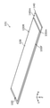
- FIG. 1 is a schematic perspective view showing the overall configuration of the semiconductor light emitting device according to the first embodiment.
- FIG. 2 is a schematic perspective view showing the overall configuration of the semiconductor light emitting device according to the first embodiment.
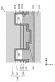
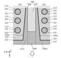
- FIG. 3 is a schematic plan view showing a configuration in the vicinity of the emission surface of the semiconductor light emitting device according to the first embodiment.
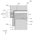
- FIG. 4 is a schematic first cross-sectional view showing the configuration of the semiconductor light emitting device according to the first embodiment.
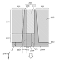
- FIG. 5 is a schematic second sectional view showing the configuration of the semiconductor light emitting device according to the first embodiment.
- FIG. 6 is a schematic third sectional view showing the configuration of the semiconductor light emitting device according to the first embodiment.
- FIG. 1 is a schematic perspective view showing the overall configuration of the semiconductor light emitting device according to the first embodiment.
- FIG. 2 is a schematic perspective view showing the overall configuration of the semiconductor light emitting device according to the first embodiment.
- FIG. 3 is a schematic plan view showing a configuration in the vicinity of the
- FIG. 7 is a schematic first cross-sectional view illustrating the operation of the semiconductor light emitting device according to the first embodiment.
- FIG. 8 is a schematic second sectional view illustrating the operation of the semiconductor light emitting device according to the first embodiment.
- FIG. 9 is a schematic plan view showing a configuration in the vicinity of the emission surface of the semiconductor light emitting device included in the semiconductor light emitting device according to the second embodiment.
- FIG. 10 is a schematic plan view showing a configuration in the vicinity of the emission surface of the semiconductor light emitting device included in the semiconductor light emitting device according to the third embodiment.
- FIG. 11 is a schematic plan view showing a configuration in the vicinity of the emission surface of the semiconductor light emitting device according to the fourth embodiment.
- FIG. 12 is a schematic cross-sectional view showing a configuration near an emission surface of the semiconductor light emitting device according to the fourth embodiment.
- FIG. 13A is a schematic cross-sectional view showing the configuration of the semiconductor light emitting device described in Patent Document 1.
- FIG. 13B is a schematic perspective view showing the configuration of the submount described in Patent Document 1.
- each figure is a schematic diagram and is not necessarily exactly illustrated. Therefore, the scales and the like do not always match in each figure.
- the same reference numerals are given to substantially the same configurations, and duplicate explanations will be omitted or simplified.
- the terms “upper” and “lower” do not refer to the upward direction (vertically upward) and the downward direction (vertically downward) in absolute spatial recognition, but are based on the stacking order in the laminated configuration. It is used as a term defined by the relative positional relationship. Also, the terms “upper” and “lower” are used not only when the two components are spaced apart from each other and another component exists between the two components, but also when the two components are present. It also applies when they are placed in contact with each other.
- 1 and 2 are schematic perspective views showing the overall configuration of the semiconductor light emitting device 100 and the semiconductor light emitting device 101 according to the present embodiment, respectively.
- FIG. 3 is a schematic plan view showing a configuration in the vicinity of the emission surface 100F of the semiconductor light emitting device 101 according to the present embodiment.
- FIG. 3 shows a plan view of the position corresponding to the inside of the dashed line frame III of FIG.
- the illustration of the submount 140 is partially omitted, and only the position of the end face of the submount 140 is shown by a broken line.
- FIG. 4 to 6 are schematic cross-sectional views showing the configuration of the semiconductor light emitting device 101 according to the present embodiment.
- FIG. 5, and FIG. 6 show cross sections of the semiconductor light emitting device 101 shown in FIG. 3 in the IV-IV line, the VV line, and the VI-VI line, respectively.
- each figure shows an X-axis, a Y-axis, and a Z-axis which are perpendicular to each other.
- a semiconductor light emitting element 100 that emits light and a semiconductor light emitting element 100 are mounted via a bonding member 130 (see FIGS. 4 to 6). It is a device including a submount 140 having a mounting surface 140 m to be mounted.
- the semiconductor light emitting device 101 further includes a joining member 130 for joining the semiconductor light emitting element 100 and the submount 140.
- the submount 140 is a base on which the semiconductor light emitting element 100 is mounted and has a high thermal conductivity, and has a function of dissipating the heat generated by the semiconductor light emitting element 100.
- the semiconductor light emitting device 100 is mounted on the submount 140 via the bonding member 130.
- the submount 140 is formed of AlN, diamond, or the like, and has a rectangular parallelepiped shape.
- the joining member 130 is not particularly limited as long as it is a member capable of joining the semiconductor light emitting device 100 and the submount 140, but is, for example, a solder containing AuSn or the like.
- the semiconductor light emitting device 100 has a semiconductor laminate 108 and a mounting electrode 114.
- the semiconductor light emitting device 100 is a multi-emitter type semiconductor laser array that emits a plurality of laser beams.
- the light emitting direction of the semiconductor light emitting device 100 is a direction parallel to the Y-axis direction in each figure.
- the light emission direction of the semiconductor light emitting device 100 corresponds to the resonance direction of the laser light.
- the semiconductor laminate 108 is a rectangular parallelepiped element, and as shown in FIG. 2, has a facing surface 100m facing the mounting surface 140m of the submount 140 and an emission surface 100F for emitting light.
- the semiconductor laminate 108 further has a rear end surface 100R facing back to the exit surface 100F.
- the facing surface 100m is a surface perpendicular to the Z-axis direction in FIG. 2
- the exit surface 100F is a surface perpendicular to the Y-axis direction in FIG.
- light resonates between the exit surface 100F and the rear end surface 100R.
- the exit surface 100F of the semiconductor laminate 108 is located outside the mounting surface 140m from the end of the mounting surface 140m of the submount 140.
- one or more mounting electrodes 114 are arranged on the facing surface 100m of the semiconductor laminate 108, and one or more grooves 120 extending in the emission direction along the mounting electrodes 114 are formed.
- a plurality of grooves 120 are formed in the semiconductor laminate 108.
- the plurality of grooves 120 are arranged in a direction perpendicular to the emission direction and parallel to the facing surface 100 m.
- Each of the plurality of grooves 120 has a pair of side walls 120a and 120b extending in the exit direction, as shown in FIGS. 3 and 4. As shown in FIG.
- the first distance L1 between the emission surface 100F of the semiconductor light emitting device 100 and each of the plurality of grooves 120 is larger than zero. That is, each of the plurality of grooves 120 is not formed on the exit surface 100F.
- the first distance L1 is more accurately between the exit surface 100F and the position closest to the exit surface 100F among each of the plurality of grooves 120 (that is, the position closest to the exit surface 100F). Defined by distance.
- the first distance L1 is smaller than the second distance L2 between the exit surface 100F and the mounting surface 140 m. The action and effect of the relationship between the first distance L1 and the second distance L2 will be described later.
- the groove 120 is formed by etching the crystal growth layer 109 by, for example, a wet etching method or a dry etching method. In this embodiment, a part of the substrate 110 is also etched.
- the semiconductor laminate 108 has a substrate 110, a crystal growth layer 109, and an insulating layer 115.
- the substrate 110 is the base of the semiconductor light emitting device 100.
- the substrate 110 is an n-type GaN substrate having a thickness of 80 ⁇ m.
- the crystal growth layer 109 is a semiconductor layer in which crystals are grown on the main surface of the substrate 110.
- the crystal growth layer 109 has a first semiconductor layer 111, a light emitting layer 112, and a second semiconductor layer 113.
- Each layer of the crystal growth layer 109 is formed by, for example, an organic metal vapor phase growth method (MOCVD) or the like.
- the first semiconductor layer 111 is a first conductive type semiconductor layer arranged above the substrate 110.
- the first conductive type is n-type
- the first semiconductor layer 111 includes an n-type clad layer made of n—Al 0.03 Ga 0.97 N having a thickness of 3 ⁇ m.
- the first semiconductor layer 111 may include a layer other than the n-type clad layer.
- the first semiconductor layer 111 may include a buffer layer or the like arranged between the substrate 110 and the n-type clad layer.
- the light emitting layer 112 is a layer arranged above the first semiconductor layer 111.
- the light emitting layer 112 is a quantum well active layer in which a well layer having a thickness of 5 nm made of In 0.06 Ga 0.94 N and a barrier layer having a thickness of 10 nm made of GaN are alternately laminated. Including, it has two well layers.
- the light emitting layer 112 may include a layer other than the quantum well active layer.
- the light emitting layer 112 may include an optical guide layer or the like.
- the second semiconductor layer 113 is a second conductive type semiconductor layer different from the first conductive type, which is arranged above the light emitting layer 112.
- the second conductive type is a p type
- the second semiconductor layer 113 is a layer having a thickness of 3 nm made of p—Al 0.06 Ga 0.94 N and a thickness of 3 nm made of GaN.
- the second semiconductor layer 113 may include a layer other than the p-type clad layer.
- the second semiconductor layer 113 may include a p-type contact layer arranged between the p-type clad layer and the mounting electrode 114. Further, as shown in FIGS. 4 to 6, a ridge portion 113r for confining light and current is formed in the second semiconductor layer 113. The ridge portion 113r is formed by etching the second semiconductor layer 113, for example, by a dry etching method.
- the insulating layer 115 is a layer formed of an insulating material arranged above the second semiconductor layer 113. An opening is formed in the insulating layer 115, and the mounting electrode 114 is arranged in the opening. The opening is formed in a portion of the insulating layer 115 on the ridge portion 113r. The surface layer of the groove 120 is also formed of the insulating layer 115.
- the insulating layer 115 is a SiO 2 layer having a thickness of 300 nm.
- the illustration of the insulating layer 115 is omitted.
- the insulating layer 115 is formed by, for example, a plasma CVD method.
- the mounting electrode 114 is an electrode that is arranged on the facing surface 100 m of the semiconductor laminate 108 and extends in the light emitting direction.
- the semiconductor light emitting device 100 has a plurality of mounting electrodes 114.
- the mounting electrode 114 has a rectangular shape in which the longitudinal direction is the light emitting direction.
- the mounting electrode 114 is a laminated film arranged above the second semiconductor layer 113 and in which Pd and Pt are laminated in order from the second semiconductor layer 113 side.
- the mounting electrode 114 is not formed near the exit surface 100F of the semiconductor laminate 108. That is, a non-injection region in which no current is injected is formed between the mounting electrode 114 and the exit surface 100F.
- the mounting electrode 114 arranged above the second semiconductor layer 113 is arranged facing the mounting surface 114m of the submount 140. That is, the semiconductor light emitting device 100 is junction-down mounted on the submount 140.
- the light emitting layer 112 having a larger heat generation amount can be arranged closer to the submount 140 than when the semiconductor light emitting element 100 is mounted in a junction-up manner, so that the heat dissipation characteristics of the semiconductor light emitting device 101 can be improved.
- the third distance L3 between the exit surface 100F and the mounting electrodes 114 is larger than zero.
- the second distance L2 between the exit surface 100F and the mounting surface 140m of the submount 140 is smaller than the third distance L3 between the exit surface 100F and the mounting electrode 114. The action and effect of the relationship between the second distance L2 and the third distance L3 will be described later.
- the mounting electrode 114 is arranged between two adjacent grooves 120 in a plan view of the facing surface 100 m of the semiconductor light emitting device 100.
- the mounting electrode 114 is arranged on the ridge portion 113r.
- the current is supplied to the portion of the light emitting layer 112 located below the mounting electrode 114. Therefore, light is generated in the portion of the light emitting layer 112 that faces the mounting electrode 114 (that is, the portion located below the ridge portion 113r).
- a back surface electrode is formed on the main surface on the back side of the main surface on which the crystal growth layer 109 of the substrate 110 is formed.
- the back surface electrode is, for example, a laminated film in which Ti, Pt, and Au are formed in this order from the substrate 110.
- the mounting electrode 114 and the back surface electrode according to this embodiment are formed by, for example, a vacuum vapor deposition method.
- FIGS. 7 and 8 are schematic cross-sectional views illustrating the operation of the semiconductor light emitting device 101 according to the present embodiment. 7 and 8 show cross sections of the semiconductor light emitting device 101 shown in FIG. 3 on the VII-VII line and the VIII-VIII line, respectively.
- the bonding member 130 arranged between the submount 140 and the semiconductor light emitting element 100 is melted by heating.
- the semiconductor light emitting element 100 is mounted on the submount 140, the semiconductor light emitting element 100 is pressed against the joining member 130 of the submount 140.
- a part of the joining member 130 arranged between the submount 140 and the mounting electrode 114 shown in FIG. 8 is pushed outward from between the submount 140 and the mounting electrode 114.
- the extruded joining member 130 flows into the groove 120 as shown in FIG. 7. Therefore, it is possible to reduce the number of joining members 130 flowing out from between the emission surface 100F of the semiconductor light emitting device 100 and the submount 140.
- the joining member 130 that has flowed into the groove 120 may flow out from between the exit surface 100F of the semiconductor light emitting element 100 and the submount 140.
- the first distance L1 between the exit surface 100F and the groove 120 is from the second distance L2 between the exit surface 100F and the mounting surface 140m of the submount 140. small. That is, the side wall 120e of the groove 120 facing back to the exit surface 100F is located outside the submount 140 from the end surface 140e of the submount 140. Therefore, the joining member 130 flowing out from between the semiconductor light emitting device 100 and the submount 140 through the groove 120 is guided to flow in the direction along the side wall 120e of the groove 120 substantially parallel to the exit surface 100F.
- the joining member 130 is guided to flow in the direction along the end surface 140e located at the end of the mounting surface 140m of the submount 140. Therefore, it is possible to prevent the joining member 130 from projecting in the vicinity of the exit surface 100F in a direction perpendicular to the exit surface 100F.
- the mounting electrode 114 near the exit surface 100F is joined to the submount 140.
- the joining member 130 is suppressed from protruding in the vicinity of the exit surface 100F as described above, the thermal conductivity is suppressed in the vicinity of the exit surface 100F of the submount 140 as in the submount described in Patent Document 1.
- the heat dissipation characteristics of the semiconductor light emitting device 101 near the emission surface 100F are not impaired.
- the second distance L2 is smaller than the third distance L3 between the exit surface 100F and the mounting electrode 114.
- the heat generated near the end of the mounting electrode 114 of the semiconductor light emitting element 100 near the exit surface 100F is not only in the direction perpendicular to the mounting surface 140m (that is, below the mounting electrode 114 in FIG. 8), but also in the sub. It is also dissipated in the direction toward the end surface 140e of the mount 140, that is, in the direction inclined with respect to the mounting surface 140 m (see the broken line arrow in FIG. 8).
- the second distance L2 is equal to or greater than the third distance L3, that is, when the mounting electrode 114 is arranged up to the end of the mounting surface 140m of the submount 140, it is close to the exit surface 100F of the mounting electrode 114.
- the heat generated near the end is dissipated only in the direction perpendicular to the mounting surface 140 m. Therefore, since the second distance L2 is smaller than the third distance L3, the heat dissipation characteristics of the semiconductor light emitting device 101 can be improved as compared with the case where the second distance L2 is the third distance L3 or more.
- the semiconductor light emitting device 101 has good heat dissipation characteristics and can suppress the joining member 130 from protruding near the emission surface 100F of the semiconductor light emitting element 100.
- the semiconductor light emitting device 100 is a multi-emitter type as in the present embodiment, the amount of heat generated by the semiconductor light emitting device 100 is further increased, but the heat dissipation characteristics of the submount 140 are good, so that the COD Occurrence can be suppressed.
- the semiconductor light emitting device according to the second embodiment will be described.
- the semiconductor light emitting device according to the present embodiment is different from the semiconductor light emitting device 101 according to the first embodiment in the shape of the groove formed in the semiconductor light emitting device.
- the semiconductor light emitting device according to the present embodiment will be described with reference to FIG. 9, focusing on the differences from the semiconductor light emitting device 101 according to the first embodiment.
- FIG. 9 is a schematic plan view showing a configuration in the vicinity of the emission surface 200F of the semiconductor light emitting device 200 included in the semiconductor light emitting device according to the present embodiment.
- FIG. 9 shows a plan view of the facing surface 200 m of the semiconductor light emitting device 200 in a plan view.
- the semiconductor light emitting device includes a semiconductor light emitting element 200 and a submount 140.
- the semiconductor light emitting device 200 includes a semiconductor laminate 208 and one or more mounting electrodes 114.
- the semiconductor laminate 208 according to the present embodiment one or more mounting electrodes 114 are arranged, and one or more grooves 220 extending in the emission direction along the mounting electrodes 114 are formed.
- the semiconductor light emitting device 200 according to the present embodiment is different from the semiconductor light emitting device 100 according to the first embodiment in the shape of the groove 220, and is the same in other configurations.
- the first portion 221 of the groove 220 adjacent to the mounting electrode 114 in the direction perpendicular to the exit direction (and the stacking direction of the semiconductor laminate 208) (that is, the X-axis direction in FIG. 9).
- the average distance D1 in the direction perpendicular to the emission direction with the mounting electrode 114 (and the stacking direction of the semiconductor laminate 208) is the second portion 222 of the groove 220 arranged closer to the emission surface than the mounting electrode 114. Is smaller than the average distance D2 in the direction perpendicular to the emission direction with the mounting electrode 114 (and the stacking direction of the semiconductor laminate 208).
- the average distance D1 between the first portion 221 of the groove 220 adjacent to the mounting electrode 114 in the X-axis direction and the ridge portion 113r of the second semiconductor layer 113 is the emission surface from the mounting electrode 114 of the groove 220. It is smaller than the average distance D2 between the second portion 222 arranged at a position close to the ridge portion 113r and the ridge portion 113r.
- the semiconductor light emitting device 200 has the above-mentioned configuration.
- the light emitting layer 112 arranged between the mounting electrode 114 and the emission surface 200F, that is, the light emitting layer 112 in the non-injection region is the light emitting layer 112 in the portion facing the mounting electrode 114, that is, the injection region.
- the average bandgap is larger than that of the light emitting layer 112 in. Therefore, since the light absorption in the light emitting layer in the non-injection region near the exit surface 200F can be reduced, the calorific value in the non-injection region becomes small. Therefore, according to the semiconductor light emitting device 200 according to the present embodiment, it is possible to suppress the generation of COD in the non-injection region.
- the shape of the side surface of the groove 220 near the mounting electrode 114 is linear in plan view, but may be curved.
- the semiconductor light emitting device according to the third embodiment will be described.
- the semiconductor light emitting device according to the present embodiment is different from the semiconductor light emitting device according to the second embodiment in the internal configuration of the groove formed in the semiconductor light emitting device.
- the semiconductor light emitting device according to the present embodiment will be described with reference to FIG. 10, focusing on the differences from the semiconductor light emitting device according to the second embodiment.
- FIG. 10 is a schematic plan view showing a configuration in the vicinity of the emission surface 300F of the semiconductor light emitting element 300 included in the semiconductor light emitting device according to the present embodiment.
- FIG. 10 shows a plan view of the facing surface 300 m facing the submount 140 of the semiconductor light emitting device 300 in a plan view.
- the semiconductor light emitting device includes a semiconductor light emitting element 300 and a submount 140.
- the semiconductor light emitting device 300 includes a semiconductor laminate 308 and one or more mounting electrodes 114.
- one or more mounting electrodes 114 are arranged, and one or more grooves 320 extending in the emission direction along the mounting electrodes 114 are formed.
- the semiconductor light emitting device 300 according to the present embodiment is different from the semiconductor light emitting device 200 according to the second embodiment in the internal configuration of the groove 320, and is the same in other configurations.
- the side wall 320a of the groove 320 includes an Au layer 322 having a higher wettability of the joining member 130 than the semiconductor laminate 308. Therefore, since the wettability of the joining member 130 on the side wall 320a of the groove 320 can be enhanced, the effect of guiding the joining member 130 to the inside of the groove 320 along the side wall 320a can be enhanced.
- each of the convex portions 321 is a columnar portion erected on the bottom surface of the groove 320.
- the convex portion 321 may be formed, for example, by leaving a portion that is not removed by etching inside the groove 320 when the groove 320 is formed by etching or the like.
- the convex portion 321 is formed by leaving a part of the second semiconductor layer 113 of the semiconductor laminate 308 as a portion that is not removed during etching.
- the convex portion 321 By forming such a convex portion 321 inside the groove 320, the contact area between the joining member 130 and the inside of the groove 320 can be increased. Therefore, the effect of inducing the joining member 130 inside the groove 320 can be further enhanced. Further, as shown in FIG. 10, the convex portion 321 may also include the Au layer 322 like the side wall 320a. Thereby, the effect of guiding the joining member 130 into the groove 320 can be further enhanced. Although not shown in FIG. 10, an insulating layer formed of SiO 2 or the like is arranged between the Au layer 322 and a semiconductor such as the second semiconductor layer 113.
- the bottom surface of the groove 320 may also include an Au layer. Thereby, the effect of guiding the joining member 130 into the groove 320 can be further enhanced.
- the Au layer 322 is used as the layer having good wettability of the joining member 130, but a metal layer such as an Ag layer, a Sn layer, a Ni layer, or a Pd layer other than the Au layer 322 may be used. good.
- the semiconductor light emitting device according to the fourth embodiment will be described.
- the semiconductor light emitting device according to the present embodiment is different from the semiconductor light emitting device 101 according to the first embodiment in that a groove is formed from the substrate side of the semiconductor light emitting device.
- the semiconductor light emitting device according to the present embodiment will be described with reference to FIGS. 11 and 12, focusing on the differences from the semiconductor light emitting device 101 according to the first embodiment.
- FIG. 11 and 12 are schematic plan views and cross-sectional views showing the configuration of the semiconductor light emitting device 401 according to the present embodiment in the vicinity of the emission surface 400F, respectively.
- FIG. 11 in order to show the configuration of the semiconductor light emitting device 400 included in the semiconductor light emitting device 401, the illustration of the submount 140 is partially omitted, and only the position of the end face of the submount 140 is shown by a broken line. ..
- FIG. 12 shows a cross section of the semiconductor light emitting device 401 shown in FIG. 11 in line XII-XII.
- the semiconductor light emitting device 401 includes a semiconductor light emitting element 400 and a submount 140. As shown in FIG. 12, the semiconductor light emitting device 401 further includes a joining member 130.
- the semiconductor light emitting device 400 has a semiconductor laminate 408, one or more mounting electrodes 419, and one or more back surface electrodes 414.
- the semiconductor laminate 408 has a substrate 410 and a crystal growth layer 409.
- the crystal growth layer 409 has a first semiconductor layer 411, a light emitting layer 412, and a second semiconductor layer 413.
- the substrate 410, the first semiconductor layer 411, the light emitting layer 412, and the second semiconductor layer 413 are the substrate 110, the first semiconductor layer 411, the light emitting layer 412, and the second semiconductor layer 100 of the semiconductor light emitting device 100 according to the first embodiment, respectively. It has the same material and thickness as the semiconductor layer 413.
- a back surface electrode 414 is arranged above the second semiconductor layer 413.
- the back surface electrode 414 has the same configuration as the mounting electrode 114 according to the first embodiment.
- the facing surface 400 m facing the submount 140 of the semiconductor laminate 408 is the main surface on the back side of the main surface on which the crystal growth layer 409 of the substrate 410 is laminated, as shown in FIG. ..
- One or more mounting electrodes 419 are arranged on the facing surface 400m, and one or more grooves 420 extending in the emission direction along the mounting electrodes 419 are formed.
- the semiconductor light emitting device 400 has a plurality of mounting electrodes 419, and a plurality of grooves 420 are formed on the facing surface 400 m.
- Each of the plurality of grooves 420 has a pair of side walls 420a and 420b extending in the exit direction, as shown in FIGS. 11 and 12.
- the first distance L1 between the emission surface 400F of the semiconductor light emitting device 400 and each of the plurality of grooves 420 is larger than zero. That is, each of the plurality of grooves 420 is not formed on the exit surface 400F. Further, the first distance L1 is smaller than the second distance L2 up to the exit surface 400F and the mounting surface 140 m.
- the groove 420 is formed in the semiconductor light emitting device 400 along the mounting electrode 419, the joining member 130 extruded at the time of mounting is grooved as in the semiconductor light emitting device 101 according to the first embodiment. It flows into 420. Therefore, it is possible to reduce the number of joining members 130 flowing out from between the emission surface 400F of the semiconductor light emitting device 400 and the submount 140.
- the third distance L3 between the exit surface 400F and the mounting electrode 419 is larger than zero.
- the second distance L2 between the exit surface 400F and the mounting surface 140m of the submount 140 is smaller than the third distance L3 between the exit surface 400F and the mounting electrode 419.
- the semiconductor light emitting element is a semiconductor laser element
- the semiconductor light emitting element is not limited to the semiconductor laser element.
- the semiconductor light emitting device may be a superluminescent diode.
- the first conductive type is n type, but may be p type.
- the semiconductor light emitting device is a multi-emitter type having a plurality of mounting electrodes, but the semiconductor light emitting device may be a single emitter type having a single mounting electrode. That is, the semiconductor light emitting device may have one or more mounting electrodes.
- a plurality of grooves are formed in the semiconductor light emitting device, but a single groove may be formed in the semiconductor light emitting device. That is, it is sufficient that one or more grooves are formed in the semiconductor light emitting device.
- the configuration near the emission surface of the semiconductor light emitting device is shown, but the vicinity of the rear end surface of the semiconductor light emitting device may have the same configuration as the vicinity of the emission surface. That is, the first distance between the rear end surface and one or more grooves may be greater than zero and less than the second distance between the rear end surface and the mounting surface of the submount. Further, the second distance may be smaller than the third distance between the rear end surface and one or more mounting electrodes. As a result, the same effect as that of each embodiment is obtained.
- the plurality of grooves are formed from the surface of the second semiconductor layer 113 to the middle of the substrate 110, but the configuration of the plurality of grooves is not limited to this.
- Each of the plurality of grooves may not be formed from the surface of the second semiconductor layer 113 to the substrate 110, and may be formed, for example, from the surface of the second semiconductor layer 113 to the middle of the first semiconductor layer 111. ..
- the semiconductor light emitting device 200 may have a single mounting electrode 114 or a plurality of mounting electrodes 114. May have a mounting electrode 114 of.
- the semiconductor light emitting device 200 has a plurality of mounting electrodes 114, only one mounting electrode 114 and the groove 220 adjacent to the mounting electrode 114 may have the configuration according to the second embodiment, or may be combined with another mounting electrode 114.
- the groove 220 adjacent to the groove 220 may also have the configuration according to the second embodiment.
- one or more mounting electrodes include a first mounting electrode
- one or more grooves include a first groove adjacent to the first mounting electrode
- the first mounting is performed in the direction perpendicular to the exit direction among the first grooves.
- the average distance between the portion adjacent to the electrode and the first mounting electrode in the direction perpendicular to the emission direction is the portion of the first groove located closer to the emission surface than the first mounting electrode and the first mounting electrode. It may be smaller than the average distance in the direction perpendicular to the emission direction of.
- the insulating layer may be formed in the region where the mounting electrode 419 is not formed in the facing surface 400 m of the semiconductor laminate 408.
- the semiconductor light emitting device of the present disclosure can be applied to a processing machine, a projector, etc. as a high output and high efficiency light source, for example.
Landscapes
- Physics & Mathematics (AREA)
- Condensed Matter Physics & Semiconductors (AREA)
- General Physics & Mathematics (AREA)
- Electromagnetism (AREA)
- Optics & Photonics (AREA)
- Led Device Packages (AREA)
- Semiconductor Lasers (AREA)
Priority Applications (3)
| Application Number | Priority Date | Filing Date | Title |
|---|---|---|---|
| DE112021004159.2T DE112021004159T5 (de) | 2020-08-04 | 2021-06-23 | Halbleiter-Lichtemissionsvorrichtung |
| JP2022541148A JPWO2022030127A1 (https=) | 2020-08-04 | 2021-06-23 | |
| US18/098,825 US20230155346A1 (en) | 2020-08-04 | 2023-01-19 | Semiconductor light emitting device |
Applications Claiming Priority (2)
| Application Number | Priority Date | Filing Date | Title |
|---|---|---|---|
| JP2020-132661 | 2020-08-04 | ||
| JP2020132661 | 2020-08-04 |
Related Child Applications (1)
| Application Number | Title | Priority Date | Filing Date |
|---|---|---|---|
| US18/098,825 Continuation US20230155346A1 (en) | 2020-08-04 | 2023-01-19 | Semiconductor light emitting device |
Publications (1)
| Publication Number | Publication Date |
|---|---|
| WO2022030127A1 true WO2022030127A1 (ja) | 2022-02-10 |
Family
ID=80117972
Family Applications (1)
| Application Number | Title | Priority Date | Filing Date |
|---|---|---|---|
| PCT/JP2021/023768 Ceased WO2022030127A1 (ja) | 2020-08-04 | 2021-06-23 | 半導体発光装置 |
Country Status (4)
| Country | Link |
|---|---|
| US (1) | US20230155346A1 (https=) |
| JP (1) | JPWO2022030127A1 (https=) |
| DE (1) | DE112021004159T5 (https=) |
| WO (1) | WO2022030127A1 (https=) |
Cited By (1)
| Publication number | Priority date | Publication date | Assignee | Title |
|---|---|---|---|---|
| WO2023182156A1 (ja) * | 2022-03-25 | 2023-09-28 | ヌヴォトンテクノロジージャパン株式会社 | 半導体発光装置、基台、半田付き基台、及び、半導体発光装置の製造方法 |
Citations (10)
| Publication number | Priority date | Publication date | Assignee | Title |
|---|---|---|---|---|
| JPH11220204A (ja) * | 1998-01-30 | 1999-08-10 | Mitsubishi Electric Corp | アレイ型半導体レーザ装置およびその製造方法 |
| JP2003037323A (ja) * | 2001-07-25 | 2003-02-07 | Sony Corp | 半導体レーザ・アレイ装置用サブマウント、半導体レーザ・アレイ装置、及びその作製方法 |
| JP2003318475A (ja) * | 2002-04-24 | 2003-11-07 | Kyocera Corp | 光半導体素子のマウント構造 |
| US20070286252A1 (en) * | 2006-06-08 | 2007-12-13 | Samsung Electronics Co., Ltd. | Submount of a multi-beam laser diode module |
| US20090104727A1 (en) * | 2007-09-20 | 2009-04-23 | Bookham Technology Plc | High power semiconductor laser diodes |
| JP2011233717A (ja) * | 2010-04-27 | 2011-11-17 | Sharp Corp | 半導体レーザ装置 |
| JP2015135911A (ja) * | 2014-01-17 | 2015-07-27 | 日本オクラロ株式会社 | 半導体光素子及び光モジュール |
| JP2015173218A (ja) * | 2014-03-12 | 2015-10-01 | 三菱電機株式会社 | 半導体レーザ光源 |
| WO2018203466A1 (ja) * | 2017-05-01 | 2018-11-08 | パナソニックIpマネジメント株式会社 | 窒化物系発光装置 |
| JP2019129217A (ja) * | 2018-01-24 | 2019-08-01 | パナソニック株式会社 | 半導体レーザ素子及び半導体レーザ装置 |
Family Cites Families (20)
| Publication number | Priority date | Publication date | Assignee | Title |
|---|---|---|---|---|
| US5627851A (en) * | 1995-02-10 | 1997-05-06 | Ricoh Company, Ltd. | Semiconductor light emitting device |
| JP2000133877A (ja) * | 1998-10-27 | 2000-05-12 | Furukawa Electric Co Ltd:The | 半導体レーザ素子 |
| JP2003198057A (ja) * | 2001-12-27 | 2003-07-11 | Sony Corp | 半導体レーザ素子及びその製造方法 |
| JP2004087866A (ja) * | 2002-08-28 | 2004-03-18 | Hitachi Ltd | 半導体光素子、その実装体および光モジュール |
| JP2005223070A (ja) * | 2004-02-04 | 2005-08-18 | Toshiba Corp | 半導体発光素子及び半導体発光装置 |
| JP2006303299A (ja) * | 2005-04-22 | 2006-11-02 | Sharp Corp | 半導体レーザ |
| JP2009283512A (ja) * | 2008-05-19 | 2009-12-03 | Panasonic Corp | 窒化物半導体レーザ |
| JP4966283B2 (ja) * | 2008-10-14 | 2012-07-04 | シャープ株式会社 | 半導体レーザ装置およびその製造方法 |
| JP2011222675A (ja) * | 2010-04-07 | 2011-11-04 | Mitsubishi Electric Corp | 半導体装置及びその製造方法 |
| WO2016129618A1 (ja) * | 2015-02-12 | 2016-08-18 | 古河電気工業株式会社 | 半導体レーザ素子およびレーザ光照射装置 |
| DE102015106712A1 (de) * | 2015-04-30 | 2016-11-03 | Osram Opto Semiconductors Gmbh | Anordnung mit einem Substrat und einem Halbleiterlaser |
| JP6700019B2 (ja) * | 2015-10-20 | 2020-05-27 | スタンレー電気株式会社 | 半導体発光素子 |
| EP3836318B1 (en) * | 2018-08-09 | 2025-10-08 | Nuvoton Technology Corporation Japan | Semiconductor light emission device and method for manufacturing semiconductor light emission device |
| WO2020174949A1 (ja) * | 2019-02-26 | 2020-09-03 | パナソニックセミコンダクターソリューションズ株式会社 | 半導体レーザ装置及び半導体レーザ素子 |
| JP7356287B2 (ja) * | 2019-08-06 | 2023-10-04 | ソニーセミコンダクタソリューションズ株式会社 | 半導体レーザ駆動装置、および、電子機器 |
| US20220263288A1 (en) * | 2019-08-26 | 2022-08-18 | Panasonic Corporation | Semiconductor laser device |
| WO2021111536A1 (ja) * | 2019-12-04 | 2021-06-10 | 三菱電機株式会社 | 半導体レーザ素子およびその製造方法、半導体レーザ装置 |
| CN115989620B (zh) * | 2020-09-04 | 2025-02-25 | 三菱电机株式会社 | 半导体激光器以及半导体激光装置 |
| WO2023153476A1 (ja) * | 2022-02-10 | 2023-08-17 | 京セラ株式会社 | 発光デバイスの製造方法および製造装置並びにレーザ素子基板 |
| CN116960725A (zh) * | 2022-04-14 | 2023-10-27 | 潍坊华光光电子有限公司 | 一种基于金锡焊料封装的热沉结构及共晶方法 |
-
2021
- 2021-06-23 JP JP2022541148A patent/JPWO2022030127A1/ja active Pending
- 2021-06-23 WO PCT/JP2021/023768 patent/WO2022030127A1/ja not_active Ceased
- 2021-06-23 DE DE112021004159.2T patent/DE112021004159T5/de not_active Withdrawn
-
2023
- 2023-01-19 US US18/098,825 patent/US20230155346A1/en active Pending
Patent Citations (10)
| Publication number | Priority date | Publication date | Assignee | Title |
|---|---|---|---|---|
| JPH11220204A (ja) * | 1998-01-30 | 1999-08-10 | Mitsubishi Electric Corp | アレイ型半導体レーザ装置およびその製造方法 |
| JP2003037323A (ja) * | 2001-07-25 | 2003-02-07 | Sony Corp | 半導体レーザ・アレイ装置用サブマウント、半導体レーザ・アレイ装置、及びその作製方法 |
| JP2003318475A (ja) * | 2002-04-24 | 2003-11-07 | Kyocera Corp | 光半導体素子のマウント構造 |
| US20070286252A1 (en) * | 2006-06-08 | 2007-12-13 | Samsung Electronics Co., Ltd. | Submount of a multi-beam laser diode module |
| US20090104727A1 (en) * | 2007-09-20 | 2009-04-23 | Bookham Technology Plc | High power semiconductor laser diodes |
| JP2011233717A (ja) * | 2010-04-27 | 2011-11-17 | Sharp Corp | 半導体レーザ装置 |
| JP2015135911A (ja) * | 2014-01-17 | 2015-07-27 | 日本オクラロ株式会社 | 半導体光素子及び光モジュール |
| JP2015173218A (ja) * | 2014-03-12 | 2015-10-01 | 三菱電機株式会社 | 半導体レーザ光源 |
| WO2018203466A1 (ja) * | 2017-05-01 | 2018-11-08 | パナソニックIpマネジメント株式会社 | 窒化物系発光装置 |
| JP2019129217A (ja) * | 2018-01-24 | 2019-08-01 | パナソニック株式会社 | 半導体レーザ素子及び半導体レーザ装置 |
Cited By (1)
| Publication number | Priority date | Publication date | Assignee | Title |
|---|---|---|---|---|
| WO2023182156A1 (ja) * | 2022-03-25 | 2023-09-28 | ヌヴォトンテクノロジージャパン株式会社 | 半導体発光装置、基台、半田付き基台、及び、半導体発光装置の製造方法 |
Also Published As
| Publication number | Publication date |
|---|---|
| US20230155346A1 (en) | 2023-05-18 |
| JPWO2022030127A1 (https=) | 2022-02-10 |
| DE112021004159T5 (de) | 2023-06-22 |
Similar Documents
| Publication | Publication Date | Title |
|---|---|---|
| JP6337036B2 (ja) | 半導体レーザダイオード | |
| US20110080932A1 (en) | Laser diode and laser diode device | |
| JP2011108932A (ja) | 光半導体装置 | |
| JP7220751B2 (ja) | 端面発光型のレーザバー | |
| US20200295533A1 (en) | Semiconductor laser diode and semiconductor component | |
| JP4966283B2 (ja) | 半導体レーザ装置およびその製造方法 | |
| WO2020225952A1 (ja) | 半導体レーザ装置および外部共振型レーザ装置 | |
| CN101656399B (zh) | 多束激光二极管 | |
| US20060249745A1 (en) | Heat dissipating structure and light emitting device having the same | |
| US10707651B2 (en) | Semiconductor laser element | |
| US20230155346A1 (en) | Semiconductor light emitting device | |
| KR101789175B1 (ko) | 방열성이 우수한 레이저 다이오드 바 모듈 | |
| JP2006303299A (ja) | 半導体レーザ | |
| JP4737387B2 (ja) | 半導体レーザ素子 | |
| JP2630206B2 (ja) | 高出力パルスレーザダイオードモジュール | |
| WO2020195282A1 (ja) | 半導体レーザ素子 | |
| JP2010098001A (ja) | 半導体レーザ装置およびその製造方法 | |
| KR101136161B1 (ko) | 레이저 다이오드 | |
| JP7245061B2 (ja) | 半導体発光装置及び半導体発光装置の製造方法 | |
| JP2019129219A (ja) | 半導体レーザ素子及び半導体レーザ装置 | |
| WO2018158934A1 (ja) | 半導体レーザ及びその製造方法 | |
| JP5503574B2 (ja) | レーザダイオード | |
| JP2008130664A (ja) | 半導体発光素子および発光装置 | |
| KR20030072994A (ko) | 광손실 및 열 특성을 개선시킨 반도체 레이저 다이오드 | |
| JP2013008791A (ja) | レーザダイオード組立体 |
Legal Events
| Date | Code | Title | Description |
|---|---|---|---|
| 121 | Ep: the epo has been informed by wipo that ep was designated in this application |
Ref document number: 21854046 Country of ref document: EP Kind code of ref document: A1 |
|
| ENP | Entry into the national phase |
Ref document number: 2022541148 Country of ref document: JP Kind code of ref document: A |
|
| 122 | Ep: pct application non-entry in european phase |
Ref document number: 21854046 Country of ref document: EP Kind code of ref document: A1 |