WO2022024756A1 - 光電気混載基板 - Google Patents
光電気混載基板 Download PDFInfo
- Publication number
- WO2022024756A1 WO2022024756A1 PCT/JP2021/026405 JP2021026405W WO2022024756A1 WO 2022024756 A1 WO2022024756 A1 WO 2022024756A1 JP 2021026405 W JP2021026405 W JP 2021026405W WO 2022024756 A1 WO2022024756 A1 WO 2022024756A1
- Authority
- WO
- WIPO (PCT)
- Prior art keywords
- optical
- electric
- wiring
- optical element
- metal reinforcing
- Prior art date
- Legal status (The legal status is an assumption and is not a legal conclusion. Google has not performed a legal analysis and makes no representation as to the accuracy of the status listed.)
- Ceased
Links
Images


Classifications
-
- G—PHYSICS
- G02—OPTICS
- G02B—OPTICAL ELEMENTS, SYSTEMS OR APPARATUS
- G02B6/00—Light guides; Structural details of arrangements comprising light guides and other optical elements, e.g. couplings
- G02B6/24—Coupling light guides
- G02B6/42—Coupling light guides with opto-electronic elements
- G02B6/4201—Packages, e.g. shape, construction, internal or external details
- G02B6/4274—Electrical aspects
- G02B6/428—Electrical aspects containing printed circuit boards [PCB]
-
- G—PHYSICS
- G02—OPTICS
- G02B—OPTICAL ELEMENTS, SYSTEMS OR APPARATUS
- G02B6/00—Light guides; Structural details of arrangements comprising light guides and other optical elements, e.g. couplings
- G02B6/10—Light guides; Structural details of arrangements comprising light guides and other optical elements, e.g. couplings of the optical waveguide type
- G02B6/12—Light guides; Structural details of arrangements comprising light guides and other optical elements, e.g. couplings of the optical waveguide type of the integrated circuit kind
- G02B6/12002—Three-dimensional structures
-
- G—PHYSICS
- G02—OPTICS
- G02B—OPTICAL ELEMENTS, SYSTEMS OR APPARATUS
- G02B6/00—Light guides; Structural details of arrangements comprising light guides and other optical elements, e.g. couplings
- G02B6/10—Light guides; Structural details of arrangements comprising light guides and other optical elements, e.g. couplings of the optical waveguide type
- G02B6/12—Light guides; Structural details of arrangements comprising light guides and other optical elements, e.g. couplings of the optical waveguide type of the integrated circuit kind
- G02B6/12004—Combinations of two or more optical elements
-
- H—ELECTRICITY
- H05—ELECTRIC TECHNIQUES NOT OTHERWISE PROVIDED FOR
- H05K—PRINTED CIRCUITS; CASINGS OR CONSTRUCTIONAL DETAILS OF ELECTRIC APPARATUS; MANUFACTURE OF ASSEMBLAGES OF ELECTRICAL COMPONENTS
- H05K1/00—Printed circuits
- H05K1/02—Details
- H05K1/0274—Optical details, e.g. printed circuits comprising integral optical means
-
- G—PHYSICS
- G02—OPTICS
- G02B—OPTICAL ELEMENTS, SYSTEMS OR APPARATUS
- G02B6/00—Light guides; Structural details of arrangements comprising light guides and other optical elements, e.g. couplings
- G02B6/24—Coupling light guides
- G02B6/42—Coupling light guides with opto-electronic elements
- G02B6/4201—Packages, e.g. shape, construction, internal or external details
- G02B6/4204—Packages, e.g. shape, construction, internal or external details the coupling comprising intermediate optical elements, e.g. lenses, holograms
- G02B6/4214—Packages, e.g. shape, construction, internal or external details the coupling comprising intermediate optical elements, e.g. lenses, holograms the intermediate optical element having redirecting reflective means, e.g. mirrors, prisms for deflecting the radiation from horizontal to down- or upward direction toward a device
-
- H—ELECTRICITY
- H05—ELECTRIC TECHNIQUES NOT OTHERWISE PROVIDED FOR
- H05K—PRINTED CIRCUITS; CASINGS OR CONSTRUCTIONAL DETAILS OF ELECTRIC APPARATUS; MANUFACTURE OF ASSEMBLAGES OF ELECTRICAL COMPONENTS
- H05K1/00—Printed circuits
- H05K1/02—Details
- H05K1/0213—Electrical arrangements not otherwise provided for
- H05K1/0237—High frequency adaptations
- H05K1/0245—Lay-out of balanced signal pairs, e.g. differential lines or twisted lines
-
- H—ELECTRICITY
- H05—ELECTRIC TECHNIQUES NOT OTHERWISE PROVIDED FOR
- H05K—PRINTED CIRCUITS; CASINGS OR CONSTRUCTIONAL DETAILS OF ELECTRIC APPARATUS; MANUFACTURE OF ASSEMBLAGES OF ELECTRICAL COMPONENTS
- H05K2201/00—Indexing scheme relating to printed circuits covered by H05K1/00
- H05K2201/20—Details of printed circuits not provided for in H05K2201/01 - H05K2201/10
- H05K2201/2009—Reinforced areas, e.g. for a specific part of a flexible printed circuit
Definitions
- the present invention relates to an optical / electric mixed substrate used for an optical communication module, and particularly to an optical / electric mixed substrate having excellent reliability for high-frequency signals.
- optical wiring has been adopted in addition to electrical wiring due to the increase in the amount of transmission information, and an optical-electric mixed mounting board in which electrical wiring and optical wiring are arranged compactly is being praised. Further, the use of the optical / electric mixed board for an optical communication module or the like for high-speed signal transmission by further connecting the optical / electric mixed board to a wiring board or the like having a signal transmission function to various electronic devices is expanding.
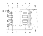
- FIG. 1 An example of such an optical communication module is schematically shown in FIG.
- This optical communication module has an optical / electric mixed board 2 integrally connected to a wiring board 1. More specifically, first, on the surface of the wiring board 1, a pair of two for differential signal transmission An electric wiring X in which a plurality of wirings are arranged is provided.
- the optical / electrical mixed substrate 2 includes an insulating layer 3 (indicated by a coarse diagonal line in the figure) including a wide portion and a narrow portion, and the back surface of the wide portion of the insulating layer 3, that is, An electric wiring Y, an optical element (VCSEL, a photodiode, etc.) 4, an optical element drive device (IC, etc.) 5 in which a plurality of two pairs of wirings for differential signal transmission are arranged on a surface overlapping the surface of the wiring board 1.
- the electric circuit unit 6 having the above is provided.
- the electric circuit portion 6 is covered with a coverlay (not shown) at a portion requiring insulation.
- a metal reinforcing layer 7 for reinforcing the electric circuit portion 6 is provided on the surface of the insulating layer 3 opposite to the surface on which the electric circuit portion 6 is provided, and the metal reinforcing layer 7 is provided.
- a band-shaped optical waveguide 8 is provided so as to partially overlap with the above.
- the electric circuit portion 6 of the optical / electric mixed substrate 2 will be described in more detail with reference to FIG. 11 in which this portion is enlarged and schematically shown (the coverlay is not shown). That is, in the electric circuit portion 6 provided on one side of the insulating layer 3, a pad 10 for mounting an optical element 4 (VCSEL, a photodiode, etc., indicated by a one-point chain wire) and a pad 10 for driving the optical element 4 are driven.
- a pad 11 for mounting a drive device 5 (indicated by a one-point chain wire such as an IC) is formed, and the electric wiring Y including the wiring portion A connecting the pads 10 and 11 is on the side where the optical waveguide 8 extends. It extends to the edge on the opposite side.
- the electric wiring Y is an electric wiring portion connecting the optical element 4 and the drive device 5 for driving the optical element 4, and electricity of the drive device 5 and the wiring board 1 (see FIG. 10) by means of a differential electric signal. It consists of an electrical wiring unit that connects the wiring X. A terminal 13 serving as a connection point with the electric wiring X is provided at the tip of the electric wiring Y.
- a metal reinforcing layer 7 is provided on the opposite surface of the insulating layer 3 provided with the electric circuit portion 6 in order to reinforce the electric circuit portion 6, and the metal reinforcing layer 7 is provided.
- An optical waveguide 8 is provided on the surface of the insulating layer 3 so as to partially overlap the metal reinforcing layer 7.
- a reflective surface for changing the path of light is formed in a portion of the optical waveguide 8 facing the optical element 4 with the insulating layer 3 interposed therebetween (not shown), and the light is reflected from the reflective surface.
- Light is optically coupled to the optical element 4.
- a through hole 14 is formed in the portion of the metal reinforcing layer 7 sandwiched between the reflective surface of the optical waveguide 8 and the light receiving / receiving portion of the optical element 4, and the metal reinforcing layer 7 obstructs the passage of light. There is no such thing.
- optical communication modules there is an increasing demand for high-speed and accurate transmission of enormous amounts of information, including image information and audio information. There is a demand for more stable transmission technology for optical signals.
- the metal reinforcing layer since the electrical characteristics at the connection points between the substrates are affected by the metal reinforcing layer, it is possible that the metal reinforcing layer does not affect the electrical characteristics of the opto-electrically mixed substrate even at places other than the above connection points. If so, what kind of improvement is possible is being investigated.
- the present invention has been made in view of such circumstances, and provides an optical-electric mixed mounting substrate capable of transmitting a higher frequency electric signal while suppressing the influence of the metal reinforcing layer on the electrical characteristics.
- an optical / electric mixed board used for an optical communication module An electric circuit provided with an insulating layer and an electric wiring Y provided on the first surface side of the insulating layer and including a pad for mounting an optical element, a pad for an optical element driving device, and a wiring portion A connecting the pads.
- a photoelectric mixed mounting substrate in which an opening is formed by removing a portion of the metal reinforcing layer facing the wiring portion A provided on the opposite side of the insulating layer.
- the present inventors have determined that the effective capacitance of the optical element mounted on the opto-electric mixed substrate is the optical element itself. It was found that the capacitance generated between the metal reinforcing layer and the wiring portion A is added in addition to the capacitance of the light, so that the capacitance is larger than that before mounting.
- the portion of the metal reinforcing layer facing the wiring portion A connecting the pad for mounting the optical element and the pad for the optical element drive device is removed to form an opening. Therefore, the capacitance between the wiring portion A through which electricity flows in the vicinity of the mounted optical element and the metal reinforcing layer on the opposite side of the insulating layer is removed. Therefore, conventionally, the effective capacitance of the optical element mounted on the opto-electrically mixed substrate has increased by the amount of the capacitance between the wiring portion A and the metal reinforcing layer. It is unaffected and the effective capacitance of the optical device is not increased by mounting. Therefore, the frequency band of the optical element after mounting the optical / electric mixed substrate can maintain the frequency band shown before mounting the optical element, and the amount of signal information that can be transmitted can be increased without slowing down. ..
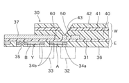
- FIG. 1 is an explanatory diagram schematically showing a main part of a photoelectric mixed mounting substrate according to an embodiment of the present invention by cutting along the extending direction of the optical waveguide.
- This optical / electric mixed board 30 is used for an optical communication module, and the basic configuration is the same as that of a general optical / electric mixed board. That is, an electric wiring Y in which a plurality of pairs of electric wirings for transmitting a differential signal are arranged on one surface (first surface) of one substantially strip-shaped insulating layer 31 as a substrate, and an optical element.
- An electric circuit unit E including a pad 34a for mounting (PD, VCSEL, etc.) 32 and a pad 34b for mounting a drive device (IC, etc.) 33 thereof is provided [FIG. 2A). See]. The portion of the electric circuit portion E that requires insulation protection is covered with the coverlay 36.
- the optical element 32 and the drive device 33 may not be attached at the stage of the substrate, and are shown by a alternate long and short dash line.
- the metal reinforcing layer 37 for reinforcing the strength of the insulating layer 31 is provided on the other surface (second surface) of the insulating layer 31, that is, the surface opposite to the side on which the electric circuit portion E is provided. However, it is partially provided in the area requiring reinforcement. Similarly, the underclad layer 40, the core 41, and the overclad layer 42 are laminated in this order on the other surface of the insulating layer 31 in an arrangement that partially overlaps with the metal reinforcing layer 37, and these three layers are used.
- An optical waveguide W is formed [see FIG. 2 (b)]. A part of the optical waveguide W is cut into an inclined surface, and the inclined surface serves as a light reflecting portion 43 for changing the traveling direction of an optical signal transmitted via the core 41 by 90 degrees. ing.
- the electric circuit section E of the optical / electric mixed board 30 will be described in more detail. That is, as shown in FIG. 2A when the optical / electric mixed board 30 is viewed from the side where the electric circuit unit E is formed, the optical element 32 shown by the diagonal line downward to the right is mounted on the electric circuit unit E. A pad 34a for mounting the pad 34a and a pad 34b for mounting the drive device 33, which is also indicated by a diagonal line downward to the right, are provided (the coverlay 36 is not shown). Further, at the end of the electric circuit unit E, a connection terminal 35 for connecting the optical / electric mixed board 30 to a wiring board having a signal transmission function to various electronic devices is provided.
- the electrical wiring Y of the electric circuit unit E includes a wiring portion A for connecting the pad 34a for the optical element 32 and the pad 34b for the drive device, and a connection terminal 35 for the pad 34b and another wiring board. It is provided with a wiring portion B for connecting to and. Of course, other wiring is also formed as needed, but the illustration is omitted.
- FIG. 2A the formation region of the metal reinforcing layer 37 provided on the surface of the insulating layer 31 opposite to the surface on which the electric circuit portion E is provided is shown by a diagonal line rising to the right.
- FIG. 2B shows the metal reinforcing layer 37 as viewed from the side on which the metal reinforcing layer 37 is formed.
- the optical waveguide W that partially overlaps with the metal reinforcing layer 37 is shown by a alternate long and short dash line.
- the metal reinforcing layer 37 is formed with a through hole 50 for optical coupling as in the conventional case, but is further provided on the opposite side with the insulating layer 31 interposed therebetween.
- the portion facing the wiring portion A connecting the pad 34a for the element 32 and the pad 34b for the drive device is removed in a substantially rectangular shape to form the opening 60. This is the greatest feature of the present invention.
- the metal reinforcing layer 37 is provided with other appropriate openings as needed, but they are not shown.
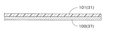
- a metal plate 100 to be a metal reinforcing layer 37 is prepared, and a photosensitive insulating resin such as polyimide is coated on the surface of the metal plate 100 to form an insulating layer 31.
- the insulating resin layer 101 is formed.
- Examples of the material of the metal plate 100 include stainless steel, copper, silver, aluminum, nickel, chromium, titanium, platinum, gold and the like, but stainless steel is preferable from the viewpoint of strength, flexibility and the like. Further, it is preferable to set the thickness of the metal reinforcing layer 37 in the range of, for example, 10 to 70 ⁇ m (more preferably 10 to 30 ⁇ m).
- the insulating resin layer 101 is subjected to a photolithography method (exposure, prebaking, development, curing) to form an insulating layer 31 having a predetermined pattern shape.
- the thickness of the insulating layer 31 is preferably set within the range of, for example, 3 to 50 ⁇ m (more preferably 3 to 25 ⁇ m) (this step is not shown).
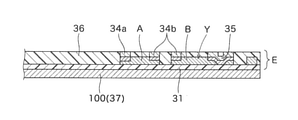
- a conductive layer made of a conductive material such as copper is formed on the insulating layer 31 by spattering or electroless plating, and then through necessary treatments such as dry film resist laminating, exposure, and development. It forms a conductive pattern such as an electric wiring Y including wiring portions A and B, various pads 34a and 34b, and a connection terminal 35. Then, as shown in FIG. 4, a photosensitive insulating resin such as polyimide is applied on the conductive pattern, and a coverlay 36 is formed in a portion requiring insulation protection in the same manner as the formation of the insulating layer 31. do.
- a metal material having excellent conductivity and expandability such as chrome, aluminum, gold, and tantalum is preferably used in addition to copper. Further, alloys using at least one of these metals are also preferably used.
- the thickness of the conductive pattern of the electric wiring Y or the like is preferably set in the range of 3 to 30 ⁇ m (more preferably 3 to 18 ⁇ m). Further, the thickness of the coverlay 36 formed on the coverlay 36 is set in the range of, for example, 1 to 50 ⁇ m (more preferably 1 to 25 ⁇ m) in consideration of insulation and protection of the electric wiring Y and the like, and further reinforcement. Is preferable.
- the electric circuit portion E can be obtained by forming an electrolytic plating layer of nickel, gold or the like on the portions of the various pads 34a and 34b and the connection terminals 35 exposed from the coverlay 36 (FIG. FIG.). See 4).
- etching treatment dry film resist laminating, exposure, development, etching, drying
- Removal of film resist, etc. is performed to remove unnecessary parts to obtain a predetermined pattern shape.
- the insulating layer 31 provided with the electric circuit portion E and the metal reinforcing layer 37 is turned upside down, and the metal reinforcing layer 37 is turned upward.
- the underclad layer 40, the core 41, and the overclad layer 42 are patterned on the surface of the insulating layer 31 on the side where the metal reinforcing layer 37 is formed by a known method, and each layer is patterned in a predetermined pattern as needed.
- the optical waveguide W can be obtained by laminating and forming in this state (see FIG. 1).
- the predetermined portion of the optical waveguide W is formed by dicing, laser processing, cutting, or the like to form the core 41.
- the light reflecting surface 43 is formed on an inclined surface inclined by 45 ° with respect to the longitudinal direction. In this way, the photoelectric mixed mounting substrate 30 shown in FIG. 1 can be obtained.
- the tip side (not shown) on the side opposite to the side facing the electric circuit portion E has a configuration in which an optical connector for connecting to another optical wiring member is attached.
- a similar electric circuit portion E' may be formed on the distal end side of the optical waveguide W.
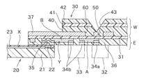
- the optical / electric mixed board 30 thus obtained is connected to a wiring board 20 used in various electric / electronic devices to form an optical communication module board, for example, as shown in FIG.
- the necessary devices are implemented to obtain an optical communication module.
- the wiring board 20 includes an insulating board 21, an electrical wiring X, a connection terminal 22, and a coverlay 23.
- the connection terminals 35 and 22 are opposed to each other so as to be vertically overlapped with each other, and the facing connection terminals 35 and 22 are electrically connected by a solder bump or the like. It is done by connecting to the target.
- the portion of the metal reinforcing layer 37 provided on one side of the insulating layer 31 faces the wiring portion A connecting the pad 34a for mounting the optical element and the pad 34b for the drive device thereof. Is removed to form the opening 60, so that the capacitance generated between the wiring portion A through which electricity flows and the metal reinforcing layer 37 in the vicinity of the mounted optical element 32 can be removed. Therefore, the effective capacitance of the optical element 32 does not increase even after being mounted on the optical / electric mixed substrate 30, and the frequency band of the optical element 32 can maintain the frequency band before mounting. can. That is, the amount of signal information that can be transmitted can be increased without slowing down.
- the optical / electric mixed mounting substrate 30 when an opening is provided in the coverlay 36 covering the wiring portion A to expose the wiring portion A connecting the optical element 32 and the drive device 33 thereof, the opening is not provided.
- the effective capacitance of the optical element 32 can be made smaller than that of the optical element 32.
- the capacitance originally possessed by the optical element 32 is smaller in the PD than in the VCSEL, the influence of the additional capacitance between the wiring portion A and the metal reinforcing layer 37 is more significant in the PD. It appears prominently. Therefore, it is particularly effective to apply the present invention when the PD is used as the optical element 32.
- the opening 60 of the metal reinforcing layer 37 has a dimension in the longitudinal direction (direction in which the wiring extends) of the wiring portion A provided on the opposite side of the insulating layer 31 [FIG. 2A).
- the opening dimension [indicated by J in FIG. 2 (b)] of the opening 60 of the metal reinforcing layer 37 along the longitudinal direction of the wiring portion A is 0.8 to 1. It is preferable to set so as to be. That is, when the opening dimension J along the longitudinal direction of the wiring portion A of the opening 60 is longer than the dimension H in the longitudinal direction of the wiring portion A, the metal reinforcing layer 37 of the portion overlapping the pads 34a and 34b partially.
- the function as a reinforcing plate is reduced. Therefore, sufficient connection strength cannot be obtained in the mounting portion, and the reliability of the connection strength in this portion is lowered in the subsequent handling, which is not preferable.
- the capacitance between the wiring portion A and the metal reinforcing layer 37 is proportional to the area of the portion where the wiring portion A and the metal reinforcing layer 37 face each other, the opening dimension J is larger than the above range. If it is too small, a non-negligible capacitance will be generated in this part. Therefore, the effective capacitance of the optical element 32 increases, and the frequency band tends to shift to the low frequency side, which is not preferable.
- the wiring portion A [FIG. 2 (a)) in which the opening 60 of the metal reinforcing layer 37 is composed of two sets of four sets of wiring corresponding to a plurality of channels arranged in parallel. In this example, it corresponds to four channels], but it was formed as one elongated opening that faces this part collectively, but the opening 60 is, for example, as shown in FIG. There may be a plurality of individual openings 60a (four in this example) that are individually opened for each. According to this configuration, since the portion of the metal reinforcing layer 37 remains as a partition between each channel, the optical element 32 and light are located in the vicinity of the opening 60, although it is inferior to the above example in terms of the effect of removing the capacitance. The reinforcing effect when mounting the element drive device 33 has an advantage that it is improved as compared with the above example.
- an opening 60 is provided in a portion facing the wiring portion A of the electric circuit portion E, but the metal reinforcing layer 37 is provided with an opening 60.
- the metal reinforcing layer 37 can be removed in a band shape along the wiring. According to this configuration, the frequency band of the wiring portion B, which is a differential electric wiring, can be made higher.
- the type of the signal flowing through the wiring portion A and the wiring portion B is not particularly limited, and an appropriate one is selected according to the type of the optical element 32 to be connected, various devices, and the like. ..
- Examples of the signal type include a single-ended signal, a differential signal, a coplanar signal, and the like.
- the opto-electric mixed mounting substrate shown in FIG. 8 was produced in the same manner as the opto-electric mixed mounting substrate 30 shown in FIGS. 1, 2 (a) and 2 (b). In the figure, the same parts are designated by the same reference numerals, and the description thereof will be omitted. Then, in the electric circuit unit E of the optical / electric mixed substrate 30, a photodiode for 25 Gbps (part number APA1201040000, manufactured by II-VI Laser Enterprise) was mounted as the optical element 32 on the pad 34a for mounting the optical element.
- a photodiode for 25 Gbps part number APA1201040000, manufactured by II-VI Laser Enterprise
- Example 1 or Comparative Example Sample 1 A high-frequency optical signal output from a high-frequency light source having a known S-parameter is input to the above-mentioned Example 1 or Comparative Example Sample 1, and a vector network analyzer (N5227A, Keysight Technology Co., Ltd.) having a 2-port configuration is used. The S parameter was obtained. Since the obtained S-parameter is a combination of the characteristics of the light source and the example sample 1 or the comparative example sample 1, it is carried out from the combined S-parameter value and the known S-parameter value of the light source. The S-parameters of Example Sample 1 or Comparative Example Sample 1 were obtained.
- a photoelectric mixed board having the same configuration as the photo-electric mixed board 30 shown in FIGS. 1, 2 (a) and 2 (b) is prepared, and the optical element for the light source is 25 Gbps.
- a VCSEL product number: APA4501040001, manufactured by II-VI Laser Enterprise
- a connector portion for optical transmission is formed at the other end of the optical waveguide W extending from the optical / electric mixed mounting substrate, and a high frequency of DC current 6 mA is obtained from the pad 34b arranged at the end of the wiring portion A extending from VCSEL (for light source).
- An electric signal was superimposed and input, and this electric signal was converted into an optical signal by the above VCSEL (for a light source), and this was used as a light source.
- a connector portion for optical transmission is formed at the other end of the optical waveguide W of the example sample 1, the connector portion is connected to the connector portion of the optical-electric mixed mounting substrate used as the light source, and input is made from the light source through the optical waveguide W.
- the optical signal generated can be converted into an electric signal by the photodiode (optical element 32) of Example Sample 1.
- the S parameter was obtained by a network analyzer while applying a DC reverse bias voltage of 2V from the pad 34b lined up at the end of the wiring portion A extending from the photodiode (optical element 32) of Example 1 above.
- Example Sample 1 Using the obtained S-parameter insertion loss and the known S-parameter insertion loss of the light source, the S-parameter insertion loss of Example Sample 1 was determined. Then, the insertion loss [response (dB)] of the normalized S parameter of Example Sample 1 is shown in FIG.
- Example sample 1 shows a high frequency band exceeding 5 GHz as compared with Comparative Example sample 1.
- the optical / electric mixed substrate having the structure of Example 1 when used in an actual optical communication module, it has excellent characteristics corresponding to an increase in communication information and a high speed.
- the optical element mounted on the substrate is not affected by the presence of the metal reinforcing layer on the back surface side, and the low capacitance originally inherent in the optical element can be maintained. can. Therefore, the frequency of the transmission signal can be increased as compared with the conventional case, and it can be widely used in high-speed signal transmission technology.
Landscapes
- Physics & Mathematics (AREA)
- Engineering & Computer Science (AREA)
- Microelectronics & Electronic Packaging (AREA)
- General Physics & Mathematics (AREA)
- Optics & Photonics (AREA)
- Optical Integrated Circuits (AREA)
- Structure Of Printed Boards (AREA)
Priority Applications (3)
| Application Number | Priority Date | Filing Date | Title |
|---|---|---|---|
| CN202180049751.0A CN115868252A (zh) | 2020-07-29 | 2021-07-14 | 光电混载基板 |
| JP2022540151A JP7682183B2 (ja) | 2020-07-29 | 2021-07-14 | 光電気混載基板 |
| US18/010,564 US12366715B2 (en) | 2020-07-29 | 2021-07-14 | Opto-electric hybrid board |
Applications Claiming Priority (2)
| Application Number | Priority Date | Filing Date | Title |
|---|---|---|---|
| JP2020128012 | 2020-07-29 | ||
| JP2020-128012 | 2020-07-29 |
Publications (1)
| Publication Number | Publication Date |
|---|---|
| WO2022024756A1 true WO2022024756A1 (ja) | 2022-02-03 |
Family
ID=80036299
Family Applications (1)
| Application Number | Title | Priority Date | Filing Date |
|---|---|---|---|
| PCT/JP2021/026405 Ceased WO2022024756A1 (ja) | 2020-07-29 | 2021-07-14 | 光電気混載基板 |
Country Status (5)
| Country | Link |
|---|---|
| US (1) | US12366715B2 (https=) |
| JP (1) | JP7682183B2 (https=) |
| CN (1) | CN115868252A (https=) |
| TW (1) | TW202208905A (https=) |
| WO (1) | WO2022024756A1 (https=) |
Families Citing this family (3)
| Publication number | Priority date | Publication date | Assignee | Title |
|---|---|---|---|---|
| TWI884282B (zh) * | 2020-06-22 | 2025-05-21 | 日商日東電工股份有限公司 | 光通訊模組基板 |
| JP2024093387A (ja) * | 2022-12-27 | 2024-07-09 | 新光電気工業株式会社 | 配線基板及びその製造方法 |
| US12446149B2 (en) * | 2023-09-26 | 2025-10-14 | Cyntec Co., Ltd. | Flexible printed circuit board with embedded optical waveguide structure |
Citations (6)
| Publication number | Priority date | Publication date | Assignee | Title |
|---|---|---|---|---|
| US5712749A (en) * | 1995-03-02 | 1998-01-27 | Hutchinson Technology Incorporated | Reduced capacitance of electrical conductor on head suspension assembly |
| JP2010266598A (ja) * | 2009-05-13 | 2010-11-25 | Hitachi Cable Ltd | 光配線部材 |
| JP2011076645A (ja) * | 2009-09-29 | 2011-04-14 | Dainippon Printing Co Ltd | サスペンション用基板、サスペンション、ヘッド付サスペンションおよびハードディスクドライブ |
| JP2016105160A (ja) * | 2014-11-25 | 2016-06-09 | 日東電工株式会社 | 光電気混載基板およびその製法 |
| JP2018146710A (ja) * | 2017-03-03 | 2018-09-20 | 日東電工株式会社 | 光導波路コア形成用感光性エポキシ樹脂組成物、光導波路コア形成用感光性フィルム、光導波路、光電気混載基板および光導波路の製造方法 |
| WO2020090200A1 (ja) * | 2018-10-30 | 2020-05-07 | 浜松ホトニクス株式会社 | 光検出装置 |
Family Cites Families (21)
| Publication number | Priority date | Publication date | Assignee | Title |
|---|---|---|---|---|
| JP4222882B2 (ja) | 2003-06-03 | 2009-02-12 | 日東電工株式会社 | 配線回路基板 |
| JP5055193B2 (ja) * | 2008-04-24 | 2012-10-24 | 日東電工株式会社 | 光電気混載基板の製造方法 |
| JP4796615B2 (ja) * | 2008-11-26 | 2011-10-19 | 日東電工株式会社 | 光電気混載基板およびその製造方法 |
| JP4754613B2 (ja) * | 2008-11-27 | 2011-08-24 | 日東電工株式会社 | 光電気混載基板およびその製造方法 |
| KR101067793B1 (ko) * | 2009-11-13 | 2011-09-27 | 삼성전기주식회사 | 연성 광기판 및 그 제조방법 |
| JP2012194401A (ja) * | 2011-03-16 | 2012-10-11 | Nitto Denko Corp | 光電気混載基板およびその製法 |
| JP5840988B2 (ja) * | 2012-03-16 | 2016-01-06 | 日東電工株式会社 | 光電気混載基板およびその製法 |
| JP5840989B2 (ja) * | 2012-03-16 | 2016-01-06 | 日東電工株式会社 | 光電気混載基板およびその製法 |
| JP5877749B2 (ja) * | 2012-03-29 | 2016-03-08 | 日東電工株式会社 | 光電気混載基板の製法 |
| JP5877756B2 (ja) * | 2012-05-08 | 2016-03-08 | 日東電工株式会社 | 光電気混載基板およびその製法 |
| JP6202662B2 (ja) * | 2012-11-27 | 2017-09-27 | 日東電工株式会社 | 光電気混載基板およびその製法 |
| JP6245569B2 (ja) * | 2013-06-06 | 2017-12-13 | 日東電工株式会社 | 光電気混載基板 |
| JP6414839B2 (ja) * | 2013-09-27 | 2018-10-31 | 日東電工株式会社 | 光電気混載基板およびその製法 |
| JP6202566B2 (ja) * | 2013-10-29 | 2017-09-27 | 日東電工株式会社 | 光電気混載基板およびその製法 |
| JP6474060B2 (ja) * | 2013-10-31 | 2019-02-27 | 日東電工株式会社 | 光電気混載基板 |
| JP6319762B2 (ja) * | 2013-10-31 | 2018-05-09 | 日東電工株式会社 | 光電気混載基板およびその製法 |
| JP6376556B2 (ja) * | 2014-06-10 | 2018-08-22 | 日東電工株式会社 | 光電気混載基板 |
| JP6712742B2 (ja) * | 2014-09-24 | 2020-06-24 | 日東電工株式会社 | 光電気混載基板およびその製法 |
| JP6460515B2 (ja) * | 2014-10-24 | 2019-01-30 | 日東電工株式会社 | 光電気混載基板およびその製法 |
| JP6460516B2 (ja) * | 2014-10-28 | 2019-01-30 | 日東電工株式会社 | 光電気混載基板 |
| JP6674691B2 (ja) * | 2014-12-10 | 2020-04-01 | 日東電工株式会社 | 光電気混載基板 |
-
2021
- 2021-07-14 CN CN202180049751.0A patent/CN115868252A/zh active Pending
- 2021-07-14 JP JP2022540151A patent/JP7682183B2/ja active Active
- 2021-07-14 TW TW110125791A patent/TW202208905A/zh unknown
- 2021-07-14 WO PCT/JP2021/026405 patent/WO2022024756A1/ja not_active Ceased
- 2021-07-14 US US18/010,564 patent/US12366715B2/en active Active
Patent Citations (6)
| Publication number | Priority date | Publication date | Assignee | Title |
|---|---|---|---|---|
| US5712749A (en) * | 1995-03-02 | 1998-01-27 | Hutchinson Technology Incorporated | Reduced capacitance of electrical conductor on head suspension assembly |
| JP2010266598A (ja) * | 2009-05-13 | 2010-11-25 | Hitachi Cable Ltd | 光配線部材 |
| JP2011076645A (ja) * | 2009-09-29 | 2011-04-14 | Dainippon Printing Co Ltd | サスペンション用基板、サスペンション、ヘッド付サスペンションおよびハードディスクドライブ |
| JP2016105160A (ja) * | 2014-11-25 | 2016-06-09 | 日東電工株式会社 | 光電気混載基板およびその製法 |
| JP2018146710A (ja) * | 2017-03-03 | 2018-09-20 | 日東電工株式会社 | 光導波路コア形成用感光性エポキシ樹脂組成物、光導波路コア形成用感光性フィルム、光導波路、光電気混載基板および光導波路の製造方法 |
| WO2020090200A1 (ja) * | 2018-10-30 | 2020-05-07 | 浜松ホトニクス株式会社 | 光検出装置 |
Also Published As
| Publication number | Publication date |
|---|---|
| JP7682183B2 (ja) | 2025-05-23 |
| TW202208905A (zh) | 2022-03-01 |
| US20230258893A1 (en) | 2023-08-17 |
| JPWO2022024756A1 (https=) | 2022-02-03 |
| CN115868252A (zh) | 2023-03-28 |
| US12366715B2 (en) | 2025-07-22 |
Similar Documents
| Publication | Publication Date | Title |
|---|---|---|
| KR101234987B1 (ko) | 가요성 기판, 광송수신 모듈 및 광송수신 장치 | |
| JP5580994B2 (ja) | 光モジュール | |
| JP4892514B2 (ja) | 光通信モジュールおよびフレキシブルプリント基板 | |
| JP7682183B2 (ja) | 光電気混載基板 | |
| JP5707879B2 (ja) | 光送信器及び中継基板 | |
| JP5247880B2 (ja) | 光電気配線基板および光モジュール | |
| JP2015172683A (ja) | 光モジュール | |
| KR20020038594A (ko) | 광·전기배선기판, 실장기판 및 광전기배선기판의 제조방법 | |
| CN112993058B (zh) | 一种基于混合集成工艺的光电微系统封装结构 | |
| JP2015515213A (ja) | 埋込誘電体及び金属導波路を用いるチップ間通信 | |
| US20240168226A1 (en) | Optical circuit board and optical component mounting structure using same | |
| CN104914517A (zh) | 光模块 | |
| JP6128859B2 (ja) | 光モジュール | |
| JP2004093606A (ja) | 光モジュール及び光伝送装置 | |
| JP7698643B2 (ja) | 光通信モジュール基板 | |
| US20230280554A1 (en) | Opto-electric hybrid board, optical communication module using same, and optical element inspection method | |
| WO2010061582A1 (ja) | 回路モジュールの基板及びその製造方法 | |
| JP4041226B2 (ja) | 光半導体装置 | |
| JP2002131565A (ja) | 実装用基板及びそれを用いたデバイスの搭載構造 | |
| US20250191824A1 (en) | Common mode filter and optical transceiver | |
| CN120858488A (zh) | 高频连接线路 | |
| JP2022026578A (ja) | 光電気混載基板 | |
| Vanwassenhove | Low‐cost fibre‐chip coupling for electro‐optic EMC‐probes | |
| JP2002196168A (ja) | 光集積回路基板 | |
| KR20000027761A (ko) | 광송수신 모듈의 고속화방법 |
Legal Events
| Date | Code | Title | Description |
|---|---|---|---|
| 121 | Ep: the epo has been informed by wipo that ep was designated in this application |
Ref document number: 21850566 Country of ref document: EP Kind code of ref document: A1 |
|
| ENP | Entry into the national phase |
Ref document number: 2022540151 Country of ref document: JP Kind code of ref document: A |
|
| NENP | Non-entry into the national phase |
Ref country code: DE |
|
| 122 | Ep: pct application non-entry in european phase |
Ref document number: 21850566 Country of ref document: EP Kind code of ref document: A1 |