WO2022009800A1 - 固体電解コンデンサ素子、ならびに固体電解コンデンサおよびその製造方法 - Google Patents
固体電解コンデンサ素子、ならびに固体電解コンデンサおよびその製造方法 Download PDFInfo
- Publication number
- WO2022009800A1 WO2022009800A1 PCT/JP2021/025153 JP2021025153W WO2022009800A1 WO 2022009800 A1 WO2022009800 A1 WO 2022009800A1 JP 2021025153 W JP2021025153 W JP 2021025153W WO 2022009800 A1 WO2022009800 A1 WO 2022009800A1
- Authority
- WO
- WIPO (PCT)
- Prior art keywords
- anode
- groove
- electrolytic capacitor
- capacitor element
- solid electrolytic
- Prior art date
- Legal status (The legal status is an assumption and is not a legal conclusion. Google has not performed a legal analysis and makes no representation as to the accuracy of the status listed.)
- Ceased
Links
Images

Classifications
-
- H—ELECTRICITY
- H01—ELECTRIC ELEMENTS
- H01G—CAPACITORS; CAPACITORS, RECTIFIERS, DETECTORS, SWITCHING DEVICES, LIGHT-SENSITIVE OR TEMPERATURE-SENSITIVE DEVICES OF THE ELECTROLYTIC TYPE
- H01G9/00—Electrolytic capacitors, rectifiers, detectors, switching devices, light-sensitive or temperature-sensitive devices; Processes of their manufacture
- H01G9/004—Details
- H01G9/04—Electrodes or formation of dielectric layers thereon
- H01G9/048—Electrodes or formation of dielectric layers thereon characterised by their structure
- H01G9/052—Sintered electrodes
-
- H—ELECTRICITY
- H01—ELECTRIC ELEMENTS
- H01G—CAPACITORS; CAPACITORS, RECTIFIERS, DETECTORS, SWITCHING DEVICES, LIGHT-SENSITIVE OR TEMPERATURE-SENSITIVE DEVICES OF THE ELECTROLYTIC TYPE
- H01G9/00—Electrolytic capacitors, rectifiers, detectors, switching devices, light-sensitive or temperature-sensitive devices; Processes of their manufacture
- H01G9/004—Details
- H01G9/04—Electrodes or formation of dielectric layers thereon
- H01G9/048—Electrodes or formation of dielectric layers thereon characterised by their structure
-
- H—ELECTRICITY
- H01—ELECTRIC ELEMENTS
- H01G—CAPACITORS; CAPACITORS, RECTIFIERS, DETECTORS, SWITCHING DEVICES, LIGHT-SENSITIVE OR TEMPERATURE-SENSITIVE DEVICES OF THE ELECTROLYTIC TYPE
- H01G9/00—Electrolytic capacitors, rectifiers, detectors, switching devices, light-sensitive or temperature-sensitive devices; Processes of their manufacture
- H01G9/0029—Processes of manufacture
- H01G9/0032—Processes of manufacture formation of the dielectric layer
-
- H—ELECTRICITY
- H01—ELECTRIC ELEMENTS
- H01G—CAPACITORS; CAPACITORS, RECTIFIERS, DETECTORS, SWITCHING DEVICES, LIGHT-SENSITIVE OR TEMPERATURE-SENSITIVE DEVICES OF THE ELECTROLYTIC TYPE
- H01G9/00—Electrolytic capacitors, rectifiers, detectors, switching devices, light-sensitive or temperature-sensitive devices; Processes of their manufacture
- H01G9/0029—Processes of manufacture
- H01G9/0036—Formation of the solid electrolyte layer
-
- H—ELECTRICITY
- H01—ELECTRIC ELEMENTS
- H01G—CAPACITORS; CAPACITORS, RECTIFIERS, DETECTORS, SWITCHING DEVICES, LIGHT-SENSITIVE OR TEMPERATURE-SENSITIVE DEVICES OF THE ELECTROLYTIC TYPE
- H01G9/00—Electrolytic capacitors, rectifiers, detectors, switching devices, light-sensitive or temperature-sensitive devices; Processes of their manufacture
- H01G9/004—Details
- H01G9/04—Electrodes or formation of dielectric layers thereon
- H01G9/042—Electrodes or formation of dielectric layers thereon characterised by the material
- H01G9/0425—Electrodes or formation of dielectric layers thereon characterised by the material specially adapted for cathode
-
- H—ELECTRICITY
- H01—ELECTRIC ELEMENTS
- H01G—CAPACITORS; CAPACITORS, RECTIFIERS, DETECTORS, SWITCHING DEVICES, LIGHT-SENSITIVE OR TEMPERATURE-SENSITIVE DEVICES OF THE ELECTROLYTIC TYPE
- H01G9/00—Electrolytic capacitors, rectifiers, detectors, switching devices, light-sensitive or temperature-sensitive devices; Processes of their manufacture
- H01G9/004—Details
- H01G9/07—Dielectric layers
-
- H—ELECTRICITY
- H01—ELECTRIC ELEMENTS
- H01G—CAPACITORS; CAPACITORS, RECTIFIERS, DETECTORS, SWITCHING DEVICES, LIGHT-SENSITIVE OR TEMPERATURE-SENSITIVE DEVICES OF THE ELECTROLYTIC TYPE
- H01G9/00—Electrolytic capacitors, rectifiers, detectors, switching devices, light-sensitive or temperature-sensitive devices; Processes of their manufacture
- H01G9/15—Solid electrolytic capacitors
Definitions
- the present disclosure relates to a solid electrolytic capacitor element, a solid electrolytic capacitor including a solid electrolytic capacitor element, and a method for manufacturing a solid electrolytic capacitor.
- the solid electrolytic capacitor includes a capacitor element provided with a solid electrolyte layer, an electrode terminal electrically connected to the capacitor element, and an exterior body for sealing the capacitor element.
- the capacitor element is, for example, an anode foil having a porous portion on the surface layer, a dielectric layer formed on at least a part of the surface of the anode foil, a solid electrolyte layer covering at least a part of the dielectric layer, and a solid. It is provided with a cathode extraction layer that covers at least a part of the electrolyte layer.
- Patent Document 1 is a surface-mounted thin capacitor using a metal foil composed of a metal core wire and an etched layer covering both sides of the metal core wire as a base material, and both ends of the metal foil are used as anodes.
- a cathode is formed on the surface of the central portion of the metal foil, and the surface-mounted thin capacitor comprises a resist resin formed at the boundary between the anode and the cathode and the inside of the etched layer in the central portion of the metal foil.
- the resist resin is on the anode side.
- a surface-mounted thin capacitor characterized by being formed so as to block between the etched layer and the conductive polymer layer.
- the solid electrolytic capacitor element includes an anode body having a porous portion on at least the surface layer and an anode body.
- a dielectric layer formed on at least a part of the surface of the anode and A cathode portion that covers at least a part of the dielectric layer is provided.
- the cathode portion includes a solid electrolyte layer that covers at least a part of the dielectric layer.
- the anode body has a first portion which is a cathode forming portion on which the solid electrolyte layer is formed, and a second portion where the solid electrolyte layer is not formed.
- the second portion includes at least an anode portion including an end of the anode body opposite to the first portion.
- the first portion is divided into a plurality of regions, and a groove portion exists at the boundary between the plurality of adjacent regions.
- the solid electrolytic capacitor according to the other aspect of the present disclosure includes at least one of the above solid electrolytic capacitor elements.
- the method for manufacturing a solid electrolytic capacitor element is as follows.
- the process of preparing (Ii) A step of forming a dielectric layer on at least a part of the surface of the anode.
- a step of forming a groove in the first portion of the anode body to divide the first portion into a plurality of regions, and (iv) at least a part of the dielectric layer in the first portion is solid.
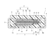
- FIG. 1 is a cross-sectional view schematically showing a solid electrolytic capacitor according to the first embodiment of the present disclosure.
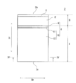
- FIG. 2 is a plan view schematically showing a solid electrolytic capacitor element included in the solid electrolytic capacitor of FIG. 1.
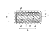
- FIG. 3 is a plan view schematically showing an anode foil included in the solid electrolytic capacitor element of FIG. 2.
- FIG. 4 is a schematic cross-sectional view taken along the line IV-IV in FIG. 2 when viewed in the direction of an arrow.
- anode body of the solid electrolytic capacitor element for example, an anode foil containing a valve acting metal and having a porous portion on the surface layer, a molded body or a sintered body of particles containing the valve acting metal is used.
- the molded body or sintered body has a porous structure as a whole, and the whole corresponds to a porous portion.
- These anodes contain many voids on the surface or throughout.
- the anode portion where the solid electrolyte layer of the anode body is not formed is connected to the electrode terminal. Therefore, air may enter the capacitor element from the electrode terminal side through the voids in the porous portion of the anode body.
- the conductive polymer contained in the solid electrolyte layer is oxidatively deteriorated or the dopant is decomposed due to the action of moisture or oxygen contained in the air, and the solid electrolyte layer is decomposed. May deteriorate and the conductivity may decrease. Deterioration of the solid electrolyte layer leads to deterioration of the performance of the solid electrolytic capacitor, such as a decrease in the capacitance of the solid electrolytic capacitor or an increase in the equivalent series resistance (ESR). Such deterioration of the solid electrolyte layer is particularly remarkable in a high temperature environment.
- Solid electrolytic capacitors may be used in high temperature environments depending on the application. Further, the solid electrolytic capacitor is generally solder-bonded to the substrate through a reflow process exposed to a high temperature. Therefore, there is a demand for a solid electrolytic capacitor element and a solid electrolytic capacitor that suppress deterioration of the solid electrolyte layer in a high temperature environment and have excellent thermal stability.
- the solid electrolytic capacitor element of the present disclosure has at least a porous portion on the surface layer, a first portion which is a cathode forming portion where the solid electrolyte layer is formed, and a second portion where the solid electrolyte layer is not formed. And have.
- the second portion includes at least an anode portion including an end opposite to the first portion of the anode body.
- the first portion is divided into a plurality of regions, and a groove portion exists at the boundary between the plurality of adjacent regions.
- the groove has a role of blocking the passage of air. Since the groove portion forms a barrier that blocks air at the boundary between the plurality of regions, it is possible to reduce the intrusion of air and the diffusion of air from the anode portion side.
- the first portion is divided into a plurality of regions by the groove portion, even if air invades from the anode portion side, the invasion (or diffusion) of air into the region divided by the groove portion can be reduced. Can be done.
- the effect of reducing the deterioration of the solid electrolyte layer is enhanced even after the solid electrolytic capacitor is exposed to a high temperature. Therefore, a decrease in capacitor performance (for example, a decrease in capacitance or an increase in ESR) after the solid electrolytic capacitor is exposed to a high temperature can be suppressed, and high thermal stability can be ensured. This makes it possible to improve the reliability of the solid electrolytic capacitor element.
- the groove is provided in at least a part of the porous portion in at least one of the thickness direction and the width direction of the anode, the ratio of the groove portion to the first portion, the width, length, and depth of the groove portion, and the groove portion.
- the effect of reducing the intrusion of air can be obtained depending on the number of divided regions and the like.
- the groove portion is at least a part of the porous portion in the thickness direction of the anode foil. It may be provided, or may be provided in the base material portion in addition to the porous portion.
- a groove portion may be provided so as to bite into a part of the base material portion from the porous portion in the thickness direction of the anode foil.
- the anode is a molded body or a sintered body, the whole is a porous portion, so that the anode is porous from the surface to the inside in at least one of the thickness direction and the width direction of the anode.
- a groove may be provided in a part of the portion.
- the anode body includes an end portion (sometimes referred to as a second end portion) on the side connected to the anode lead terminal (in the case of a molded body or a sintered body, the side into which the anode lead is inserted). It includes an end portion (sometimes referred to as a first end portion) on the side of the first portion (that is, the cathode forming portion) opposite to the second end portion.
- the anode portion will include an end portion (that is, a second end portion) opposite to the first end portion.
- the length direction of the anode body may be the center of the end face of the first end portion of the anode body (hereinafter, may be referred to as the first end face) and the end face of the second end portion (hereinafter, may be referred to as the second end face). It is the direction along the straight line connecting the center in).
- a foil-like or plate-like anode usually comprises a pair of main surfaces that occupy most of the surface of the anode, with the pair of main surfaces perpendicular to the length of the anode. It is called the width direction of the anode body. Further, the direction perpendicular to both the length direction and the width direction of the anode body is referred to as a thickness direction.
- the thickness direction of the anode foil is the thickness direction of the anode body.
- the width and the thickness of the anode are not extremely different, so that either of them may be the width direction (or the thickness direction).
- the solid electrolytic capacitor and the solid electrolytic capacitor element (hereinafter, may be simply referred to as a capacitor element) of the present disclosure, and the method for manufacturing the solid electrolytic capacitor will be described more specifically with reference to the drawings as necessary. ..
- Solid electrolytic capacitors include one or more capacitor elements.
- the anode body may have a first portion divided into a plurality of regions by a groove portion as described above.
- the anode body has a first portion divided into a plurality of regions by a groove portion, and in 75% or more, a plurality of regions due to the groove portion. It is more preferable to have a first portion divided into a plurality of regions, and it is further preferable to have a first portion divided into a plurality of regions by a groove portion in all the capacitor elements.
- the ratio of the total projected area of the groove portion in the depth direction to the effective area of the cathode portion is preferably 0.002% or more, and even if it is 0.01% or more or 0.1% or more. good.
- the total ratio of the projected area of the groove portion is, for example, 50% or less, 30% or less, or 20% or less.
- the total ratio of the projected area of the groove portion is in such a range, it is easy to secure a relatively high capacity.
- the effective area of the cathode portion is the projected area when the solid electrolyte layer on the surface side is positively projected onto each surface other than the first end face and the second end face of the anode body, and the solid electrolyte for each surface is obtained. It means the sum of the projected areas of the layers.
- the projected area of the cathode portion at the end face in the width direction is sufficiently smaller than the projected area of the cathode portion on the pair of main surfaces occupying most of the surface of the anode foil.
- the projected area of the cathode portion is the total projected area when the cathode portion on the surface side of each of the pair of main surfaces is orthographically projected, as the effective area of the cathode portion. do.
- the total projected area of the groove portion is the total projected area when all the groove portions are orthographically projected onto each surface of the anode body provided with the groove portion. be.
- the effective area of the cathode portion is obtained for the capacitor element in a state where the solid electrolytic capacitor is disassembled, the capacitor element is taken out, and the surface layer of the capacitor element is scraped off as necessary to expose the solid electrolyte layer.
- Digital images are taken from the vertical direction of each surface other than the first end face and the second end face of the anode body of the condenser element, and the cathode part and the other parts are separated by binarization processing to separate the cathode part.
- the effective area can be obtained by calculating the area of the portion and summing it for each surface.
- the projected area of the groove can be estimated from the image of a scanning electron microscope (SEM) or an optical microscope having a cross section in which the groove of the condenser element can be observed. From the cross-sectional image, the width of the opening of the groove and the length of the groove are measured for each groove, and the area of the opening of the groove obtained from these values corresponds to the projected area of the groove. By summing the projected areas of all the grooves for each surface, the total value of the projected areas of the grooves can be obtained. The width of the opening of the groove can be measured from an image of a cross section that crosses the groove, and the length of the groove can be measured from an image of a cross section along the length direction of the groove.
- SEM scanning electron microscope
- optical microscope having a cross section in which the groove of the condenser element can be observed. From the cross-sectional image, the width of the opening of the groove and the length of the groove are measured for each groove, and the area of the opening of the groove obtained from these values corresponds to the projected
- the groove When the surface of the first portion is viewed perpendicular to the surface, the groove may be formed in a curved shape, but from the viewpoint of being more easily formed, the groove is preferably linear. ..
- the groove portion can be formed, for example, by grooving at least a part of the surface layer of the first portion.
- the groove may be formed by mechanical groove processing, but when the groove is formed by laser processing, the periphery of the groove is melted to form a melted portion along the groove. It is preferable that the melted portion is formed along the groove portion because the effect of blocking air is further enhanced.
- the molten portion is a portion having a dense structure having a lower porosity than the porous portion.
- the first portion may be divided into a plurality of regions by a groove portion, but from the viewpoint of further reducing the intrusion of air from the anode portion side, it is preferable that the first portion is divided into three or more regions. It may be divided into one or more areas, or may be divided into ten or more areas. The upper limit of the number of divided regions is not particularly limited, and if the ratio of the total projected area of the groove portion in the depth direction to the effective area of the cathode portion is within the above range. good.
- the first portion may be divided into, for example, 30 or less regions, or may be divided into 20 or less regions. These lower limit values and upper limit values can be arbitrarily combined.
- the direction intersecting the length direction of the anode body (width direction, etc.) It is preferable that at least a groove extending along the) is formed.
- the groove portion extending in such a direction may be referred to as a first groove portion.
- the first portion may be provided with a second groove portion formed so as to intersect the first groove portion. Examples of the second groove portion include a groove portion extending along the length direction of the anode body.
- the first portion when focusing on one surface of the first portion, at least two first groove portions extending linearly and at least two second groove portions intersecting with these first groove portions and extending linearly. If provided, a region surrounded by a groove can be formed. In this case, the first portion is divided into a grid pattern by the groove portion. When the first portion is divided in a grid pattern, the intrusion of air into the divided region can be further suppressed. In these cases, the deterioration of the solid electrolyte layer when the solid electrolytic capacitor is exposed to a high temperature can be further reduced, so that the effect of improving the thermal stability can be further enhanced.
- the shape of the region divided by the groove when the surface of the first portion is viewed from the direction perpendicular to the surface is not particularly limited.
- the first portion may include, for example, a polygonal region divided by a groove when the surface of the first portion is viewed from a direction perpendicular to the surface, and a quadrangle divided by the groove (a first portion). It may include areas of at least one shape selected from the group consisting of rectangles, squares, parallelograms, rhombuses, trapezoids, and the like).
- the depth of the groove is, for example, less than 0.5 Tt and 0, where Tt is the length of the anode (more specifically, the thickness or width of the anode) in the direction along the depth direction of the groove. It may be .45 Tt or less or 0.4 Tt or less. When the depth of the groove is in such a range, it is easy to secure a relatively high strength of the anode while reducing the intrusion of air.
- the depth of the groove portion is, for example, 0.1 Tt or more, and may be 0.2 Tt or more. When the depth of the groove is in such a range, the intrusion of air can be further reduced.
- the depth of the groove portion is preferably 0.95 Tp or more, and is preferably 0.98 Tp or more. More preferred.
- the depth of the groove is, for example, 1.5 Tp or less, and may be 1.2 Tp or less.
- the depth of the groove is the maximum depth of the groove required in the SEM image of the cross section of the capacitor element that crosses the groove.
- the thickness (or width) Tt of the anode body is an average value of values measured at a plurality of locations (for example, 5 locations) in the region where the groove portion is not formed in the first portion.
- the thickness Tp of the porous portion is an average value of the thickness of the porous portion measured at a plurality of locations (for example, 5 locations) in the region where the groove portion of the first portion is not formed.
- the width of the groove portion may be, for example, 1 ⁇ m or more and 3 mm or less, 1 ⁇ m or more and 1.5 mm or less, 1 ⁇ m or more and 100 ⁇ m or less, 1 ⁇ m or more and 50 ⁇ m or less, or 1 ⁇ m or more and 30 ⁇ m or less for each groove portion. May be. When the width of the groove portion is within such a range, the intrusion of air from the anode portion side can be further reduced, and it is easy to secure a certain level of strength.
- the width of the groove is the width of the opening of the groove measured in the SEM image of the cross section of the capacitor element that crosses the groove.
- the width of the first groove portion can be measured by using an image of a cross section parallel to the length direction of the anode body and perpendicular to the width direction.
- the width of the second groove portion can be measured by using an image of a cross section parallel to the width direction of the anode body and perpendicular to the length direction.
- the shape of the groove is not particularly limited.
- the groove may be slit-shaped or may be recessed.
- the cross-sectional shape of the groove portion is not particularly limited, and may be V-shaped, U-shaped, or the like.
- the groove portion may be covered with an insulating material (hereinafter, may be referred to as a first insulating material).
- a first insulating material In this case, even if air invades from the anode portion side, it is difficult for the air to pass through due to the first insulating material, so that the invasion of air into the inside of the capacitor element is further reduced.
- the groove portion is reinforced by the first insulating material, the stress applied to the groove portion can be relaxed.
- the first insulating material may cover at least a part of the region of the groove, the first insulating material may be arranged on at least a part of the inner surface of the groove, and the first insulating material may be placed in the groove. It may be at least partially filled. Further, when the porous portion is present around the groove portion, the first insulating material may be contained in the porous portion around the groove portion (for example, impregnated).
- a solid electrolyte layer may be arranged in at least a part of the groove portion.
- the solid electrolyte layer may cover at least a part of the region of the groove, the solid electrolyte layer may be arranged on at least a part of the inner surface of the groove, and the solid electrolyte layer may be at least partially in the groove. May be filled (or invaded) in.
- the constituent components of the solid electrolyte layer penetrate into the groove portion, so that the solid electrolyte layer is arranged in the groove portion.
- a separation part may be provided between the anode part and the cathode forming part which is the first part.
- the capacitor element usually includes an insulating material (hereinafter, may be referred to as a second insulating material) in at least a part of the separated portion.
- a second insulating material may be arranged on the surface of the separation portion, may be contained in the porous portion of the separation portion, or may be both of them.
- the second insulating material When the second insulating material is arranged on the surface of the separation portion, the second insulating material suppresses the creeping up of the conductive polymer to the second portion side when forming the solid electrolyte layer, and the anode. The contact between the part and the cathode part is restricted.
- the separated portion is a region of the anode body from the end portion of the second insulating material on the second end side to the end portion of the first portion on the second end side.
- the separated portion may be provided with a recess whose thickness is smaller than the thickness of the anode body of the first portion (the average thickness obtained according to the above-mentioned thickness Tt).
- the recess is formed by compressing the porous portion or removing a part of the porous portion. Since the recessed portion has fewer air passages than the porous portion, the provision of the recessed portion can further reduce the intrusion of air into the condenser element from the anode portion side.
- a compressed porous portion also referred to as a compression portion in the lower region of the recess (for example, between the recess and the base material portion).
- a porous portion may be present between the concave portion and the base material, but the porous portion is made so that air is difficult to pass through. Is preferably absent.
- the recess is a portion where the thickness of the anode body is smaller than the thickness of the anode body of the first portion (the average thickness obtained according to the case of the above thickness Tt) in the separated portion.
- the second insulating material may be arranged on the surface of the recess. By arranging the second insulating material in the recess, the intrusion of air can be further reduced. Further, it becomes easier to secure the insulation between the anode portion and the cathode portion, and the stress applied to the concave portion can be alleviated by the second insulating material.
- the cathode portion of the capacitor element has a certain thickness due to having a plurality of layers, there is a step or a recess (a step or recess) between the portion on the cathode portion (or the first portion) side of the second portion and the cathode portion.
- a neck it may be referred to as a neck. Therefore, at least a part of the region extending from the cathode portion (or the first portion) side portion of the second portion to the second portion side portion of the cathode portion may be referred to as an insulating material (hereinafter, referred to as a third insulating material). .) May be covered.
- the anode has a separation portion
- at least a part of the region extending from the portion on the cathode portion (or the first portion) side of the separation portion to the portion on the second portion side of the cathode portion is covered with the third insulating material. May be good.
- the third insulating material By covering at least a part of the neck with the third insulating material, it is possible to reduce the intrusion of air from the neck into the inside of the capacitor element. It is also possible to relieve the stress applied to the neck.
- the third insulating material may cover at least a part of the surface of the solid electrolyte layer which is not covered by the cathode extraction layer.
- the third insulating material may cover a portion other than the neck (for example, the surface of the cathode portion other than the neck (for example, the entire surface of the cathode portion)) in addition to the neck portion.
- a part of the third insulating material may be impregnated in the cathode drawer layer, the solid electrolyte layer, the first portion of the anode body, and the like.
- FIG. 1 is a cross-sectional view schematically showing the structure of the solid electrolytic capacitor according to the first embodiment of the present disclosure.
- FIG. 2 is a plan view schematically showing a state in which the capacitor element included in the solid electrolytic capacitor of FIG. 1 is viewed from the surface side of one of a pair of main surfaces occupying most of the surface area of the anode foil. be.
- FIG. 3 is a plan view schematically showing a state when the anode foil included in the condenser element of FIG. 2 is viewed from one main surface side of the anode foil.
- FIG. 4 is a schematic cross-sectional view of the capacitor element of FIG. 2 in line IV-IV when viewed from the direction of the arrow.
- the solid electrolytic capacitor 1 includes a capacitor element 2, an exterior body 3 that seals the capacitor element 2, and an anode lead terminal 4 and a cathode lead terminal 5 whose at least a part thereof is exposed to the outside of the exterior body 3, respectively. ing.
- the exterior body 3 has a substantially rectangular parallelepiped outer shape, and the solid electrolytic capacitor 1 also has a substantially rectangular parallelepiped outer shape.
- the capacitor element 2 includes an anode foil 6, a dielectric layer (not shown) covering the surface of the anode foil 6, and a cathode portion 8 covering the dielectric layer.
- the dielectric layer may be formed on at least a part of the surface of the anode foil 6.
- the cathode portion 8 includes a solid electrolyte layer 9 and a cathode extraction layer 10.
- the solid electrolyte layer 9 is formed so as to cover at least a part of the dielectric layer.
- the cathode extraction layer 10 is formed so as to cover at least a part of the solid electrolyte layer 9.
- the cathode extraction layer 10 has a first layer 11 which is a carbon layer and a second layer 12 which is a metal paste layer.
- the cathode lead terminal 5 is electrically connected to the cathode portion 8 via an adhesive layer 14 formed of a conductive adhesive.
- the anode foil 6 includes a base material portion 6a and a porous portion 6b formed on the surface of the base material portion 6a.
- the anode foil 6 includes a first portion I, which is a cathode forming portion on which the solid electrolyte layer 9 (or the cathode portion 8) is formed, and a second portion II other than the first portion I.
- the second part II includes at least the anode portion ia.
- the anode lead terminal 4 is electrically connected to the anode portion ia of the anode foil 6 by welding.
- the anode foil 6 has a second end IIe on the side connected to the anode lead terminal 4 and a first end Ie on the side opposite to the second end IIe.
- the second part II includes a separation part iib in addition to the anode part ia.
- the separation portion iib is located between the anode portion ia and the first portion I.
- the second insulating material i2 is arranged on the surface of the separating portion iib, but the present invention is not limited to this case, and the separating portion iib may be provided with at least a part of the second insulating material i2.
- the second insulating material i2 such as an insulating tape may be arranged on the surface of the separating portion iib, or the film of the second insulating material i2 may be formed on the surface of the separating portion iib.
- the second insulating material i2 may be contained (for example, impregnated) in the porous portion of the separation portion iib.
- the capacitor element 2 may include both the second insulating material i2 arranged on the surface of the separating portion ib and the second insulating material i2 included in the separating portion ib.
- the first portion I of the anode foil 6 has a main surface of the anode foil 6 along the width direction DW of the anode foil 6 when viewed from a direction perpendicular to the surface.
- a first groove g1 a plurality of linearly extending, intersecting the first groove g1, and the second groove g2 of the plurality extending in a straight line along the length direction D L is provided.
- the first portion I is divided into a plurality of regions in a grid pattern by providing a plurality of first groove portions g1 and a plurality of second groove portions g2 that intersect each other.
- a first groove portion g1 or a second groove portion g2 exists at the boundary of a plurality of adjacent regions.
- the first portion I is divided into 16 regions on one of the main surfaces.
- the first portion I is divided into a plurality of regions by the first groove portion g1 and the second groove portion g2, thereby reducing the intrusion of air into the capacitor element 2 from the anode portion ia side. can do. Therefore, even when the solid electrolytic capacitor 1 is exposed to a high temperature, deterioration of the capacitor performance is suppressed and high thermal stability can be ensured.
- each of the four regions located in the center of the 16 regions is in a state of being surrounded by the first groove portion g1 and the second groove portion g2. In the area surrounded by the groove, the intrusion of air is further reduced.
- each of the first groove portion g1 and the second groove portion g2 is formed so as to partially bite into the base material portion 6a in addition to the porous portion 6b of the surface layer.
- each of the first groove portion g1 and the second groove portion g2 may be provided only on the surface layer.
- each of the first groove portion g1 and the second groove portion g2 may be formed in a part of the thickness direction DT of the porous portion 6b, or may be formed in the entire thickness of the porous portion 6b.
- each of the first groove portion g1 and the second groove portion g2 is filled with the solid electrolyte layer 9.
- the solid electrolyte layer 9 does not necessarily have to be filled in each of the first groove portion g1 and the second groove portion g2, and may be arranged in at least a part of the region in each of the first groove portion g1 and the second groove portion g2. Just do it.
- the stress applied to the first groove portion g1 and the second groove portion g2 can be relaxed.
- a step (neck) is formed in the vicinity of the boundary between the cathode portion 8 (or the first portion I) and the second portion II. Therefore, at least a part of the region extending from the portion of the second portion II on the cathode portion 8 side to the portion of the cathode portion 8 on the second portion II side may be covered with the third insulating material i3. As a result, at least a part of the step (neck) is covered with the third insulating material i3, so that it is possible to reduce the intrusion of air from this part and alleviate the stress applied to the step (neck). be able to.
- the exterior body 3 covers a part of the capacitor element 2 and the lead terminals 4 and 5. From the viewpoint of suppressing the intrusion of air into the exterior body 3, it is desirable that the capacitor element 2 and a part of the lead terminals 4 and 5 are sealed with the exterior body 3.
- FIG. 1 shows a case where the exterior body 3 is a resin exterior body, but the present invention is not limited to this case, and the exterior body 3 may be a case capable of accommodating the capacitor element 2.
- the resin exterior body is formed by sealing a part of the capacitor element 2 and the lead terminals 4 and 5 with a resin material.
- One end of the lead terminals 4 and 5 is electrically connected to the capacitor element 2, and the other end is pulled out to the outside of the exterior body 3.
- one end side of the lead terminals 4 and 5 is covered with the exterior body 3 together with the capacitor element 2.
- the solid electrolyte layer 9 is filled in each of the first groove portion g1 and the second groove portion g2, but the present invention is not limited to these cases.
- at least a part of the surface of each of the first groove portion g1 and the second groove portion g2 may be covered with the first insulating material.
- Each groove may be at least partially filled with a first insulating material. Also in these cases, the intrusion of air from the anode portion ia side into the inside of the capacitor element 2 can be further reduced, and the stress applied to the first groove portion g1 and the second groove portion g2 can be relaxed.
- both the first insulating material and the solid electrolyte layer 9 may be arranged in each of the first groove portion g1 and the second groove portion g2.
- the solid electrolyte layer 9 may be at least partially filled in each groove portion in which at least a part of the inner surface is covered with the first insulating material.
- the capacitor element includes an anode, a dielectric layer, and a cathode, respectively.
- the cathode portion includes at least a solid electrolyte layer, and may include a cathode extraction layer that covers the solid electrolyte layer in addition to the solid electrolyte layer.
- the capacitor element may include at least one selected from the group consisting of the first insulating material, the second insulating material, and the third insulating material described above.
- the anode body can include a valve acting metal, an alloy containing a valve acting metal, a compound containing a valve acting metal, and the like. These materials can be used alone or in combination of two or more.
- the valve acting metal for example, aluminum, tantalum, niobium, and titanium are preferably used.
- the anode body having a porous portion on the surface layer can be obtained by, for example, roughening the surface of a base material (such as a foil-shaped or plate-shaped base material) containing a valve acting metal by etching or the like. The roughening can be performed by, for example, an etching process.
- the anode body may be a molded body of particles containing a valve acting metal or a sintered body thereof. Each of the molded body and the sintered body has a porous structure.
- the dielectric layer is an insulating layer that functions as a dielectric.
- the dielectric layer is formed by anodizing the valvening metal on the surface of the anode.
- the dielectric layer may be formed so as to cover at least a part of the anode body.
- the dielectric layer is usually formed on the surface of the anode. Since the dielectric layer is formed on the surface of the porous portion of the anode body, it is formed along the inner wall surface of holes and depressions (also referred to as pits) on the surface of the anode body.
- the dielectric layer contains an oxide of the valve acting metal.
- the dielectric layer when tantalum is used as the valve acting metal contains Ta 2 O 5
- the dielectric layer when aluminum is used as the valve acting metal contains Al 2 O 3 .
- the dielectric layer is not limited to this, and may be any one that functions as a dielectric.
- an insulating resin (sometimes referred to as a first insulating resin) or the like is used.
- a curable resin or a cured product (including a semi-cured product) of the composition thereof is preferable as the first insulating material.
- the curable resin may be thermosetting or photocurable. Examples of the photocurable resin or a composition thereof include those that are cured by ultraviolet rays, visible light, or the like. From the viewpoint of making it easier to penetrate into the groove, it is preferable to use a photocurable (particularly, ultraviolet curable) resin or a composition thereof.
- the curable resin composition may contain, in addition to the curable resin, at least one selected from the group consisting of, for example, a curing agent, a curing accelerator, a catalyst, and an additive.
- the curable resin (sometimes referred to as the first curable resin) used as the first insulating material
- examples of the curable resin (sometimes referred to as the first curable resin) used as the first insulating material include epoxy resin, phenol resin, unsaturated polyester resin, thermosetting polyurethane resin, and thermosetting polyimide. However, it is not limited to these.
- the first curable resin may be used alone or in combination of two or more.
- the first curable resin may be a one-component curable type or a two-component curable type.
- an insulating resin (sometimes referred to as a second insulating resin) or the like is used.
- the second insulating material may contain one kind of the second insulating resin, or may contain two or more kinds.
- the second insulating material arranged on the surface of the separation portion examples include, but are limited to, an insulating tape containing the second insulating resin (resist tape, etc.), a coating film containing the second insulating resin, and the like. is not it.
- the second insulating resin contained in such a second insulating material may be a thermoplastic resin (or a thermoplastic resin composition), and may be a curable resin (may be referred to as a second curable resin). Alternatively, it may be a cured product (including a semi-cured product) of the composition.
- the thermoplastic resin as the second insulating resin include polyolefins, polyesters, polyamides, and thermoplastic polyimides.
- the second curable resin may be thermosetting or photocurable.
- Examples of the photocurable resin or a composition thereof include those that are cured by ultraviolet rays, visible light, or the like.
- Examples of the second curable resin or a composition thereof include epoxy resins, polyimides, photoresists and the like.
- the composition of the second curable resin may contain, in addition to the second curable resin, at least one selected from the group consisting of, for example, a curing agent, a curing accelerator, a catalyst, and an additive.
- the porous portion of the separation portion contains the second insulating material
- examples of such a second insulating material include those described for the first insulating material.
- a curable resin also referred to as a second curable resin
- a composition thereof particularly a photocurable (particularly, ultraviolet curable) resin or a composition thereof is used. It is preferable to use it.
- the description about the first curable resin can be referred to.
- the second insulating material the same material as the first insulating material may be used, or a different material may be used.
- an insulating resin also referred to as a third insulating resin
- the third insulating material may be a thermoplastic resin, a curable resin (also referred to as a third curable resin), or a cured product (including a semi-cured product) of the composition thereof.
- the third insulating material may contain one kind of the third insulating resin, or may contain two or more kinds.
- thermoplastic resin as the third insulating resin examples include vinyl resin (for example, vinyl chloride, vinyl acetate, aromatic vinyl resin), polyolefin (for example, polyethylene and polypropylene), acrylic resin, polyamide, polycarbonate, and thermoplastic. At least one selected from the group consisting of polyimide and polyamideimide can be mentioned.
- aromatic vinyl resin examples include polystyrene and acrylonitrile-butadiene-styrene copolymer (ABS resin).
- the description of the first curable resin can be referred to.
- the same material as the first insulating material may be used, or a different material may be used.
- the same material as the second insulating material may be used, or a different material may be used.
- the cathode portion includes a solid electrolyte layer that covers at least a part of the dielectric layer and a cathode extraction layer that covers at least a part of the solid electrolyte layer.
- the cathode portion is formed on the surface of at least a part of the first portion of the anode foil via a dielectric layer.
- the solid electrolyte layer and the cathode extraction layer will be described.
- the solid electrolyte layer is formed on the surface of the first portion of the anode.
- the solid electrolyte layer may be arranged in at least a part of the groove portion of the anode.
- the solid electrolyte layer contains a conductive polymer.
- the solid electrolyte layer may further contain at least one selected from the group consisting of dopants and other additives, if desired.
- dopant include, but are not limited to, paratoluenesulfonic acid, naphthalenesulfonic acid, and polystyrene sulfonic acid (PSS).
- the conductive polymer for example, a ⁇ -conjugated polymer can be used.
- the conductive polymer include polymers having polypyrrole, polythiophene, polyaniline, polyfuran, polyacetylene, polyphenylene, polyphenylene vinylene, polyacene, and polythiophene vinylene as basic skeletons.
- the above polymers also include homopolymers, copolymers of two or more monomers, and derivatives thereof (such as substituents having substituents).
- polythiophene includes poly (3,4-ethylenedioxythiophene) and the like. However, these are merely specific examples, and the conductive polymer is not limited to these specific examples.
- the solid electrolyte layer may be formed so as to cover at least a part of the dielectric layer.
- the solid electrolyte layer may be formed directly on the dielectric layer or may be formed via a conductive precoat layer.
- the precoat layer is formed of, for example, a conductive material (conductive polymer, inorganic conductive material, etc.).
- the conductive material constituting the precoat layer is not particularly limited, and for example, a known material can be used.
- the cathode extraction layer may include at least a first layer that comes into contact with the solid electrolyte layer and covers at least a part of the solid electrolyte layer, and may include a first layer and a second layer that covers the first layer. good.
- the first layer include a layer containing conductive particles, a metal foil, and the like.
- the conductive particles include at least one selected from conductive carbon and metal powder.
- the cathode drawer layer may be formed by a layer containing conductive carbon as the first layer (also referred to as a carbon layer) and a layer containing metal powder or a metal foil as the second layer. When a metal leaf is used as the first layer, the cathode drawer layer may be formed of this metal leaf.
- Examples of the conductive carbon include graphite (artificial graphite, natural graphite, etc.).
- the layer containing the metal powder as the second layer can be formed, for example, by laminating a composition containing the metal powder on the surface of the first layer.
- a second layer include a metal paste layer formed by using a composition containing a metal powder such as silver particles and a resin (binder resin).
- a resin binder resin
- a thermoplastic resin can be used, but it is preferable to use a thermosetting resin such as an imide resin or an epoxy resin.
- the type of metal is not particularly limited, but it is preferable to use a valve acting metal such as aluminum, tantalum, niobium, or an alloy containing a valve acting metal. If necessary, the surface of the metal foil may be roughened.
- the surface of the metal foil may be provided with a chemical conversion film, or may be provided with a metal (dissimilar metal) or non-metal film different from the metal constituting the metal foil. Examples of the dissimilar metal and the non-metal include a metal such as titanium and a non-metal such as carbon (conductive carbon and the like).
- the coating film of the above-mentioned dissimilar metal or non-metal may be used as the first layer, and the above-mentioned metal foil may be used as the second layer.
- a separator When the metal foil is used for the cathode drawer layer, a separator may be arranged between the metal foil and the anode foil.
- the separator is not particularly limited, and for example, a non-woven fabric containing fibers of cellulose, polyethylene terephthalate, vinylon, polyamide (for example, aromatic polyamide such as aliphatic polyamide and aramid) may be used.
- the solid electrolytic capacitor may be a wound type and may be a chip type or a laminated type.
- a solid electrolytic capacitor may include a laminate of two or more capacitor elements. The configuration of the capacitor element may be selected according to the type of the solid electrolytic capacitor.
- one end of the cathode lead terminal is electrically connected to the cathode lead-out layer.
- the cathode lead terminal is bonded to the cathode layer, for example, via a conductive adhesive applied to the cathode layer.
- One end of the anode lead terminal is electrically connected to the anode foil.
- the lead terminal used in the solid electrolytic capacitor can be used without particular limitation, and for example, one called a lead frame may be used. Examples of the material of each lead terminal include metal (copper and the like) or an alloy thereof.
- the solid electrolytic capacitor includes, for example, a capacitor element and a resin outer body or a case for sealing the capacitor element.
- the case include a combination of a container such as a bottomed case and a sealing body for sealing the opening of the container.
- the material constituting each of the container and the encapsulant include a metal material and a resin material.
- the resin exterior preferably contains a cured product of a curable resin composition, and may contain a thermoplastic resin or a composition containing the same.
- the curable resin composition contains, for example, a curable resin and a filler.
- a thermosetting resin is preferable.
- the resin material constituting the case include a thermoplastic resin or a composition containing the same.
- the metal material constituting the case include metals such as aluminum, copper, and iron, or alloys thereof (including stainless steel and brass).
- the capacitor element is sealed with the other end of the anode lead terminal and the other end of the cathode lead terminal drawn out from the resin exterior or the case, respectively.
- the other end of each terminal exposed from the resin exterior or the case is used for solder connection with a substrate (not shown) on which a solid electrolytic capacitor should be mounted.
- a step of preparing a capacitor element for example, a step of preparing a capacitor element (first step), a step of electrically connecting a lead terminal to the capacitor element (second step), and a part of the capacitor element and the lead terminal are exteriorized. It can be manufactured by a manufacturing method including a step of covering with (third step). Hereinafter, each step will be described in more detail.
- the first step is (i) a step of preparing an anode, (ii) a step of forming a dielectric layer, (iii) a step of forming a groove in the anode, and (iv) a step of forming a solid electrolyte layer. If necessary, (v) a step of forming a cathode lead-out layer can be included.
- the first step may further include step (vi) of applying the first insulating material to at least a part of the groove portion after step (iii) and before step (iv).
- a second insulating material is applied to the region between the anode portion and the first portion to form a separation portion. It may include a step of providing (vii). The first step may further include a step (viii) of applying a third insulating material to the neck after the step (v).
- Step of preparing the anode (i) an anode body having a porous portion at least on the surface layer and having a first portion which is a cathode forming portion and a second portion including at least an anode portion is prepared.
- the porous portion can be formed, for example, by roughening the surface of a metal foil or metal plate containing a valve acting metal, and is provided on the surface layer of the anode body.
- an unroughened base material portion is formed inside the metal foil or the metal plate, and the porous portion is formed on the surface of the base material portion.
- the roughening may be performed as long as irregularities can be formed on the surface layer of the metal foil or the metal plate, and may be performed, for example, by etching the surface of the metal foil (for example, electrolytic etching).
- a molded body or a sintered body of particles containing a valve acting metal may be prepared as an anode body.
- a recess may be formed in the region between the anode portion and the first portion of the anode body corresponding to the separating portion in this step.
- a second insulating material is arranged on the surface of the formed recess in the step (vi) described later.
- Such recesses can be formed, for example, by compressing or removing at least a portion of the porous portion in the region between the anode portion and the first portion of the anode. If necessary, compression and decompression may be combined. Compression can be performed by press working or the like. The porous portion can be removed by mechanical grooving, laser machining, or the like.
- the recesses do not necessarily have to be formed in this step, but may be formed after this step and before the second insulating material is placed on the surface.
- a dielectric layer is formed on the anode body.
- the dielectric layer is formed by anodizing the anode.
- Anodization can be carried out by a known method, for example, chemical conversion treatment or the like.
- the chemical conversion treatment can be performed, for example, by immersing the anode body in the chemical conversion liquid and applying a voltage between the anode body as the anode and the cathode immersed in the chemical conversion liquid.
- the chemical conversion liquid for example, it is preferable to use an aqueous phosphoric acid solution or the like.
- step (ii) may be performed in one step or in multiple steps. For example, when the step (iii) is performed after the step (ii), it is preferable to perform the step (ii) again after the step (iii). Similarly, when the above-mentioned recess is formed after the step (ii), the step (ii) may be performed again after forming the recess, if necessary. The step (ii) is performed before the steps (iv) to (viii).
- a groove can be formed by grooving the surface of the first portion of the anode.
- the grooving include mechanical grooving using a blade and the like, and laser machining. By using laser processing, the groove can be easily formed.
- the groove portion in the first portion, can be formed by irradiating a part of the porous portion with a laser beam.
- a pulse laser For laser processing, for example, it is preferable to use a pulse laser.
- a pulse laser By using a pulse laser, a groove can be formed and a molten portion can be easily formed along the groove. Therefore, the intrusion of air can be further reduced.
- the pulse energy may be, for example, 1 ⁇ J or more and 20 ⁇ J or less, 3 ⁇ J or more and 15 ⁇ J or less, or 5 ⁇ J or more and 10 ⁇ J or less.
- the pulse energy is in such a range, the groove portion can be formed and the melted portion is likely to be formed along the groove portion. Therefore, the intrusion of air can be further reduced.
- Step (iii) may be performed before step (iv) and steps (vi) to (viii), may be performed after step (ii), or may be performed as a sub-step in step (i). good.
- Step of applying the first insulating material In this step, the first insulating material is applied to at least a part of the groove portion. Step (vi) is performed after step (ii) and step (iii) and before step (iv).
- the first insulating material may be applied so as to cover at least a part of the groove portion.
- the groove may be impregnated or filled with the first insulating material.
- the first insulating material may be applied to the peripheral portion of the groove portion as well.
- the first insulating material may be adhered to the surface of the portion around the groove portion, or may be impregnated into the porous portion around the groove portion.
- the application of the first insulating material is carried out using at least one selected from the group consisting of known methods such as coating or dispensing methods using various coaters or dispensers, immersion and transfer (roller transfer, etc.). Will be.
- the first insulating material is applied to the groove in a state of having fluidity.
- the curable resin or the composition thereof may be applied.
- a treatment liquid containing the first insulating material and the liquid medium specifically, a solution or a dispersion liquid (coating agent or the like)
- the curable resin or the composition thereof applied to the groove may be cured in at least one of this step and the subsequent steps, if necessary.
- Step of providing a separation part by adding a second insulating material (vii))
- a second insulating material is applied to the region between the anode portion and the first portion, and at least a part thereof is provided with a separating portion having the second insulating material.
- Step (vii) is performed after step (ii) and before step (iv).
- the second insulating material is applied in the region between the anode portion and the first portion, for example, by arranging the second insulating material on the surface of the anode body or impregnating the porous portion.
- a second insulating material may be arranged on the surface of the recess.
- the second insulating material may be arranged by attaching an insulating tape (resist tape or the like) to the surface of the anode body.
- the second insulating material is a curable resin or a cured product of the composition
- the second insulating material may be arranged by applying the curable resin or the composition to the surface of the anode. good.
- a treatment liquid containing the second insulating material and a liquid medium is applied to the surface of the anode and dried to dispose of the second insulating material. You may.
- a second insulating material having fluidity for example, a curable resin or a composition thereof, a second insulating material
- a treatment liquid for example, a treatment liquid or the like
- the porous portion may contain a second insulating material.
- the second insulating material may be arranged on the surface of the anode body, and the porous portion may be impregnated with the second insulating material having fluidity.
- the second insulating material arranged on the surface of the anode and the second insulating material impregnated in the porous portion may be the same or different. Either the arrangement of the second insulating material or the impregnation of the second insulating material may be performed first.
- a curable resin or a composition thereof When a curable resin or a composition thereof is used as the second insulating material, it may be cured in at least one of this step and the subsequent steps, if necessary.
- Step of forming a solid electrolyte layer (iv))
- a solid electrolyte layer is formed so as to cover at least a part of the dielectric layer.
- the solid electrolyte layer is formed by, for example, polymerizing the precursor on the dielectric layer using a treatment liquid containing the precursor of the conductive polymer.
- the polymerization can be carried out by at least one of chemical polymerization and electrolytic polymerization.
- a conductive precoat layer may be formed prior to electrolytic polymerization.
- the precursor of the conductive polymer include at least one selected from the group consisting of monomers, oligomers and prepolymers.
- the solid electrolyte layer may be formed by attaching a treatment liquid (for example, a dispersion liquid or a solution) containing a conductive polymer to the dielectric layer and then drying the layer.
- a treatment liquid for example, a dispersion liquid or a solution
- the dispersion medium include water, an organic solvent, or a mixture thereof.
- the treatment liquid may further contain other components (such as at least one selected from the group consisting of dopants and additives).
- a solid electrolyte layer can be placed in the region.
- the cathode extraction layer is formed by forming at least the first layer on the solid electrolyte layer.
- the cathode extraction layer may be formed by sequentially stacking the first layer and the second layer.
- the cathode extraction layer is formed so as to cover at least a part of the solid electrolyte layer. In this way, the cathode portion including the solid electrolyte layer and the cathode extraction layer is formed.
- the first layer (carbon layer) containing conductive carbon may be, for example, immersed in an anode having a dielectric layer in which a solid electrolyte layer is formed in a dispersion liquid containing conductive carbon, or may contain conductive carbon. It can be formed by applying the paste to the surface of the solid electrolyte layer.
- the layer containing the metal powder as the second layer can be formed, for example, by laminating a paste-like composition containing the metal powder on the surface of the first layer.
- a composition containing a metal powder such as silver particles and a resin (binder resin) is used.
- the metal foil When a metal foil is used as the first layer, the metal foil is laminated on the solid electrolyte layer with a separator interposed between the anode and the metal foil, if necessary. If necessary, the surface of the metal foil may be roughened by etching or the like. A coating containing at least one selected from the group consisting of dissimilar metals and non-metals (such as conductive carbon) and at least one of chemical conversion coatings may be formed on the surface of the metal foil.
- a film containing at least one selected from the group consisting of dissimilar metals and non-metals (such as conductive carbon) is formed on the surface of the solid electrolyte layer as the first layer, and a metal foil is formed on the surface of the first layer. It may be laminated as a layer.
- Step of applying the third insulating material (viii) In this step, the third insulating material is applied to at least a part of the region extending from the portion on the cathode portion side of the second portion to the portion on the second portion side of the cathode portion.
- a step or a recess (neck) is formed in such a region depending on the thickness of the cathode portion, so that at least a part of the neck is covered with the third insulating material by the step (viii). Become.
- the third insulating material is applied to at least a part of the region extending from the cathode portion side portion of the second portion to the second portion side portion of the cathode portion in a state of having fluidity.
- the third insulating material covering at least a part of this region is a curable resin or a cured product of the composition thereof
- the curable resin or the composition thereof is applied in a state of having fluidity.
- a treatment liquid containing the second insulating material and the liquid medium specifically, a solution or a dispersion liquid (coating agent or the like) may be applied to at least a part of the above region to dry the liquid medium.
- the third insulating material can be added, for example, by using the method described for the first insulating material. If necessary, the surface of the cathode portion is covered with the third insulating material by immersing the neck of the capacitor element obtained in step (v) and the entire cathode portion in the third insulating material in a fluid state. You may. A part of the third insulating material may be in a state of being impregnated in the cathode drawer layer, the solid electrolyte layer, the first portion of the anode body and the like in the neck portion and the cathode portion.
- the step (viii) may be performed after the step (v).
- the step (viii) is performed before the third step.
- the step (viii) may be performed before connecting the anode lead terminal to the anode portion in the second step, or may be performed after that.
- a curable resin or a composition thereof When a curable resin or a composition thereof is used as the third insulating material, it may be cured in at least one of this step and the subsequent steps, if necessary.
- the capacitor elements are laminated in the first step (in other words, before the second step) by laminating the capacitor elements after manufacturing each capacitor element. You may prepare your body.
- the anode lead terminal and the cathode lead terminal are electrically connected to the capacitor element.
- the connection of each lead terminal may be performed after the capacitor element is manufactured in the first step.
- the connection of the cathode lead terminal to the capacitor element is performed after the capacitor element is manufactured, but the connection of the anode lead terminal to the anode body may be performed at an appropriate stage in the process of manufacturing the capacitor element.
- the anode lead terminal can be connected to the anode body in the same manner as above.
- the cathode lead terminal may be connected to a capacitor element in the same manner as described above, or one end of the cathode lead terminal may be connected to a laminate of a plurality of capacitor elements electrically connected to each other.
- the capacitor element is sealed with the exterior body by covering a part of the capacitor element and the lead terminal with the exterior body. Sealing can be performed depending on the type of exterior body.
- a part of the anode lead terminal and the cathode lead terminal connected to the capacitor element and the capacitor element is replaced with a raw material resin (for example, a curable resin composition, a thermoplastic resin or a composition thereof) of the resin exterior body. It can be sealed by covering it with an object) and molding it into a predetermined shape.
- the resin exterior body can be formed by using molding techniques such as injection molding, insert molding, compression molding, and transfer molding. At this time, the portion on the other end side of each lead terminal drawn out from the capacitor element is sealed in an exposed state.
- the condenser element is housed in the container and the other end of the lead terminal connected to the condenser element is used as the sealing body. It can be sealed by covering the opening of the container with a sealing body in a state of being pulled out from the formed through port.
- the solid electrolytic capacitor according to the present disclosure has high thermal stability, and deterioration of capacitor performance (for example, increase in ESR, decrease in capacitance) when exposed to high temperature is reduced. Therefore, it can be used for various purposes such as applications requiring low ESR and high capacitance of solid electrolytic capacitors, and applications exposed to heat. These uses are merely examples and are not limited thereto.
- Solid electrolytic capacitor 2 Condenser element 3: Exterior body 4: Anode lead terminal 5: Cathode lead terminal, 6: Anode foil, 6a: Base material part, 6b: Porous part, 8: Cathode part, 9: Solid electrolyte layer, 10: Cathode extraction layer, 11: 1st layer (carbon layer), 12: 2nd layer (metal paste layer), 14: Adhesive layer, g1: 1st groove, g2: 2nd groove, i2: 2nd insulating material, i3: 3rd insulating material, I: 1st part, II: 2nd part, ia: anode part, iib: separation part
Landscapes
- Engineering & Computer Science (AREA)
- Power Engineering (AREA)
- Microelectronics & Electronic Packaging (AREA)
- Manufacturing & Machinery (AREA)
- Chemical & Material Sciences (AREA)
- Chemical Kinetics & Catalysis (AREA)
- Electrochemistry (AREA)
- Materials Engineering (AREA)
- Fixed Capacitors And Capacitor Manufacturing Machines (AREA)
- Electric Double-Layer Capacitors Or The Like (AREA)
Priority Applications (3)
| Application Number | Priority Date | Filing Date | Title |
|---|---|---|---|
| JP2022535298A JPWO2022009800A1 (https=) | 2020-07-07 | 2021-07-02 | |
| US18/001,679 US12340955B2 (en) | 2020-07-07 | 2021-07-02 | Solid electrolytic capacitor element having improved thermal stability, and solid electrolytic capacitor and method for manufacturing same |
| CN202180048656.9A CN115917687A (zh) | 2020-07-07 | 2021-07-02 | 固体电解电容器元件和固体电解电容器及其制造方法 |
Applications Claiming Priority (2)
| Application Number | Priority Date | Filing Date | Title |
|---|---|---|---|
| JP2020-117402 | 2020-07-07 | ||
| JP2020117402 | 2020-07-07 |
Publications (1)
| Publication Number | Publication Date |
|---|---|
| WO2022009800A1 true WO2022009800A1 (ja) | 2022-01-13 |
Family
ID=79552613
Family Applications (1)
| Application Number | Title | Priority Date | Filing Date |
|---|---|---|---|
| PCT/JP2021/025153 Ceased WO2022009800A1 (ja) | 2020-07-07 | 2021-07-02 | 固体電解コンデンサ素子、ならびに固体電解コンデンサおよびその製造方法 |
Country Status (4)
| Country | Link |
|---|---|
| US (1) | US12340955B2 (https=) |
| JP (1) | JPWO2022009800A1 (https=) |
| CN (1) | CN115917687A (https=) |
| WO (1) | WO2022009800A1 (https=) |
Cited By (1)
| Publication number | Priority date | Publication date | Assignee | Title |
|---|---|---|---|---|
| WO2023189222A1 (ja) * | 2022-03-30 | 2023-10-05 | 株式会社村田製作所 | 電極箔、コンデンサ素子、および、固体電解コンデンサ |
Citations (3)
| Publication number | Priority date | Publication date | Assignee | Title |
|---|---|---|---|---|
| JPS59132629U (ja) * | 1983-02-25 | 1984-09-05 | 日本電気株式会社 | 固体電解コンデンサ |
| JP2007305661A (ja) * | 2006-05-09 | 2007-11-22 | Nippon Chemicon Corp | 固体電解コンデンサ及びその製造方法 |
| JP2008186842A (ja) * | 2007-01-26 | 2008-08-14 | Nippon Chemicon Corp | 固体電解コンデンサおよびその製造方法 |
Family Cites Families (21)
| Publication number | Priority date | Publication date | Assignee | Title |
|---|---|---|---|---|
| US3345545A (en) * | 1964-11-27 | 1967-10-03 | Johnson Matthey & Mallory Ltd | Solid electrolytic capacitor having minimum anode impedance |
| JP3863232B2 (ja) * | 1996-09-27 | 2006-12-27 | ローム株式会社 | 固体電解コンデンサに使用するコンデンサ素子の構造及びコンデンサ素子におけるチップ体の固め成形方法 |
| JP2004241455A (ja) * | 2003-02-04 | 2004-08-26 | Nec Tokin Corp | 固体電解コンデンサ用陽極体とその製造方法及びこれを用いた固体電解コンデンサ |
| US7207103B2 (en) * | 2003-12-08 | 2007-04-24 | Kemet Electronics Corporation | Powder compaction press for capacitor anodes |
| JP2005216929A (ja) | 2004-01-27 | 2005-08-11 | Nec Tokin Corp | 表面実装薄型コンデンサ及びその製造方法 |
| US7116548B2 (en) * | 2004-04-23 | 2006-10-03 | Kemet Electronics Corporation | Fluted anode with minimal density gradients and capacitor comprising same |
| CN101180693B (zh) * | 2005-05-18 | 2011-10-26 | 三洋电机株式会社 | 层叠型固体电解电容器及其制造方法 |
| US7154742B1 (en) * | 2006-05-10 | 2006-12-26 | Kemet Electronics Corporation | Fluted anode with improved capacitance and capacitor comprising same |
| JP2007311531A (ja) * | 2006-05-18 | 2007-11-29 | Nichicon Corp | 固体電解コンデンサ |
| JP2010135750A (ja) * | 2008-10-31 | 2010-06-17 | Sanyo Electric Co Ltd | 固体電解コンデンサ及びその製造方法 |
| JP2010171304A (ja) * | 2009-01-26 | 2010-08-05 | Panasonic Corp | 部品内蔵基板の製造方法 |
| JP5858802B2 (ja) * | 2012-01-24 | 2016-02-10 | ニチコン株式会社 | 電解コンデンサの製造方法 |
| US8982536B2 (en) * | 2012-10-12 | 2015-03-17 | Kemet Electronics Corporation | Anode geometry with improved volumetric efficiency and improved ESR |
| US9959979B2 (en) * | 2013-02-19 | 2018-05-01 | Kemet Electronics Corporation | Low ESR capacitor |
| US9240285B2 (en) * | 2013-04-29 | 2016-01-19 | Avx Corporation | Multi-notched anode for electrolytic capacitor |
| US9865400B2 (en) * | 2015-07-15 | 2018-01-09 | Murata Manufacturing Co., Ltd. | Capacitor |
| WO2017026316A1 (ja) * | 2015-08-12 | 2017-02-16 | 株式会社村田製作所 | コンデンサおよびその製造方法 |
| JP7113285B2 (ja) * | 2017-01-13 | 2022-08-05 | パナソニックIpマネジメント株式会社 | 電解コンデンサ |
| US11328874B2 (en) * | 2019-05-17 | 2022-05-10 | KYOCERA AVX Components Corporation | Solid electrolytic capacitor |
| CN111009419B (zh) * | 2019-09-26 | 2022-05-10 | 宇启材料科技南通有限公司 | 一种涂层电极箔及制作方法和电解电容器 |
| US12406814B2 (en) * | 2020-07-07 | 2025-09-02 | Panasonic Intellectual Property Management Co., Ltd. | Solid electrolytic capacitor element, solid electrolytic capacitor and method for producing same |
-
2021
- 2021-07-02 WO PCT/JP2021/025153 patent/WO2022009800A1/ja not_active Ceased
- 2021-07-02 CN CN202180048656.9A patent/CN115917687A/zh active Pending
- 2021-07-02 JP JP2022535298A patent/JPWO2022009800A1/ja not_active Withdrawn
- 2021-07-02 US US18/001,679 patent/US12340955B2/en active Active
Patent Citations (3)
| Publication number | Priority date | Publication date | Assignee | Title |
|---|---|---|---|---|
| JPS59132629U (ja) * | 1983-02-25 | 1984-09-05 | 日本電気株式会社 | 固体電解コンデンサ |
| JP2007305661A (ja) * | 2006-05-09 | 2007-11-22 | Nippon Chemicon Corp | 固体電解コンデンサ及びその製造方法 |
| JP2008186842A (ja) * | 2007-01-26 | 2008-08-14 | Nippon Chemicon Corp | 固体電解コンデンサおよびその製造方法 |
Cited By (1)
| Publication number | Priority date | Publication date | Assignee | Title |
|---|---|---|---|---|
| WO2023189222A1 (ja) * | 2022-03-30 | 2023-10-05 | 株式会社村田製作所 | 電極箔、コンデンサ素子、および、固体電解コンデンサ |
Also Published As
| Publication number | Publication date |
|---|---|
| US12340955B2 (en) | 2025-06-24 |
| US20230223203A1 (en) | 2023-07-13 |
| CN115917687A (zh) | 2023-04-04 |
| JPWO2022009800A1 (https=) | 2022-01-13 |
Similar Documents
| Publication | Publication Date | Title |
|---|---|---|
| JP7576746B2 (ja) | 電解コンデンサおよびその製造方法 | |
| JP7617379B2 (ja) | 固体電解コンデンサおよびその製造方法 | |
| JP7489624B2 (ja) | 電解コンデンサおよびその製造方法 | |
| CN101471185B (zh) | 漏电流小的固体电解电容器及其制造方法 | |
| US10032567B2 (en) | Solid-state electrolytic capacitor manufacturing method and solid-state electrolytic capacitor | |
| JP7792584B2 (ja) | 固体電解コンデンサ素子および固体電解コンデンサ | |
| CN108140493A (zh) | 固体电解电容器以及固体电解电容器的制造方法 | |
| US11417471B2 (en) | Solid electrolytic capacitor and production method thereof | |
| WO2022009800A1 (ja) | 固体電解コンデンサ素子、ならびに固体電解コンデンサおよびその製造方法 | |
| JP7756312B2 (ja) | 固体電解コンデンサ素子、ならびに固体電解コンデンサおよびその製造方法 | |
| US11508528B2 (en) | Electrolytic capacitor and method for producing same | |
| CN114868216B (zh) | 电容器元件及电解电容器、以及它们的制造方法 | |
| WO2023032603A1 (ja) | 固体電解コンデンサ用電極箔、それを用いた固体電解コンデンサ素子、および固体電解コンデンサ |
Legal Events
| Date | Code | Title | Description |
|---|---|---|---|
| 121 | Ep: the epo has been informed by wipo that ep was designated in this application |
Ref document number: 21837001 Country of ref document: EP Kind code of ref document: A1 |
|
| ENP | Entry into the national phase |
Ref document number: 2022535298 Country of ref document: JP Kind code of ref document: A |
|
| NENP | Non-entry into the national phase |
Ref country code: DE |
|
| 122 | Ep: pct application non-entry in european phase |
Ref document number: 21837001 Country of ref document: EP Kind code of ref document: A1 |
|
| WWG | Wipo information: grant in national office |
Ref document number: 18001679 Country of ref document: US |