WO2022009792A1 - 低接着性生体デバイス - Google Patents
低接着性生体デバイス Download PDFInfo
- Publication number
- WO2022009792A1 WO2022009792A1 PCT/JP2021/025114 JP2021025114W WO2022009792A1 WO 2022009792 A1 WO2022009792 A1 WO 2022009792A1 JP 2021025114 W JP2021025114 W JP 2021025114W WO 2022009792 A1 WO2022009792 A1 WO 2022009792A1
- Authority
- WO
- WIPO (PCT)
- Prior art keywords
- thin film
- polymer thin
- adhesive
- biological device
- biological
- Prior art date
- Legal status (The legal status is an assumption and is not a legal conclusion. Google has not performed a legal analysis and makes no representation as to the accuracy of the status listed.)
- Ceased
Links
Images











Classifications
-
- A—HUMAN NECESSITIES
- A61—MEDICAL OR VETERINARY SCIENCE; HYGIENE
- A61B—DIAGNOSIS; SURGERY; IDENTIFICATION
- A61B5/00—Measuring for diagnostic purposes; Identification of persons
- A61B5/24—Detecting, measuring or recording bioelectric or biomagnetic signals of the body or parts thereof
- A61B5/25—Bioelectric electrodes therefor
-
- A—HUMAN NECESSITIES
- A61—MEDICAL OR VETERINARY SCIENCE; HYGIENE
- A61B—DIAGNOSIS; SURGERY; IDENTIFICATION
- A61B5/00—Measuring for diagnostic purposes; Identification of persons
- A61B5/24—Detecting, measuring or recording bioelectric or biomagnetic signals of the body or parts thereof
- A61B5/25—Bioelectric electrodes therefor
- A61B5/263—Bioelectric electrodes therefor characterised by the electrode materials
-
- A—HUMAN NECESSITIES
- A61—MEDICAL OR VETERINARY SCIENCE; HYGIENE
- A61B—DIAGNOSIS; SURGERY; IDENTIFICATION
- A61B5/00—Measuring for diagnostic purposes; Identification of persons
- A61B5/24—Detecting, measuring or recording bioelectric or biomagnetic signals of the body or parts thereof
- A61B5/25—Bioelectric electrodes therefor
- A61B5/263—Bioelectric electrodes therefor characterised by the electrode materials
- A61B5/266—Bioelectric electrodes therefor characterised by the electrode materials containing electrolytes, conductive gels or pastes
-
- A—HUMAN NECESSITIES
- A61—MEDICAL OR VETERINARY SCIENCE; HYGIENE
- A61N—ELECTROTHERAPY; MAGNETOTHERAPY; RADIATION THERAPY; ULTRASOUND THERAPY
- A61N1/00—Electrotherapy; Circuits therefor
- A61N1/02—Details
- A61N1/04—Electrodes
Definitions
- the present invention relates to a low-adhesive biological device, a polymer thin film for reducing the adhesiveness of the adhesive gel of the biological device, and a method of reducing the adhesiveness of the adhesive gel of the biological device.
- Bioelectrodes are used to measure these biological signals.
- a bioelectrode is used by attaching it to the affected area.
- the bioelectrode, glucose sensor, pH sensor, ion sensor, gas sensor, thermometer, acceleration sensor and strain sensor also have an electrode portion as a constituent member thereof, and the electrode portion is adhered to the skin or the like with an adhesive gel. It is used (Non-Patent Document 1).
- Non-Patent Document 2 Non-Patent Document 3
- An object of the present invention is to provide a low-adhesive biological device that can not only reduce adhesiveness but also maintain the ability to send and receive electrical signals as electrodes.
- the present inventors have developed a low-adhesion biological device. Specifically, a polymer thin film having a thickness of several tens to 2000 nm made of a polymer material is attached onto the adhesive gel of a biological device such as a bioelectrode, while reducing the adhesiveness of the adhesive gel.
- a biological device such as a bioelectrode
- the present invention is a low-adhesive biological device having reduced adhesiveness to a biological part to be adhered, wherein the biological device is adhered to an electrode portion and an electrode surface of the electrode portion.
- a living body having a gel layer and a polymer thin film laminated on the surface of the adhesive gel layer, and maintaining the ability to send and receive electrical signals to and from the living body, while having a reduced adhesive strength than that of the adhesive gel layer.
- a biological device having adhesiveness to.
- the polymer thin film may be formed of a plurality of layers.
- the film thickness of the polymer thin film may be 50 to 2000 nm.
- the ratio of the adhesive force of the biological device to the living body to the adhesive force of the adhesive gel layer to the living body may be 10 to 90%.
- the biological device may be selected from a biological electrode, a glucose sensor, a pH sensor, an ion sensor, a gas sensor, a thermometer, an acceleration sensor or a strain sensor.
- the biological device of the present invention may be a biological device for preventing or alleviating skin disorders caused by the adhesive gel layer.
- the present invention is a polymer thin film laminated on the surface of the adhesive gel layer of the biological device, which is a polymer for reducing the adhesiveness of the adhesive gel of the biological device while retaining the transmission and reception of electric signals. Provides a thin film.
- the polymer thin film of the present invention may be formed of a plurality of layers.
- the film thickness of the polymer thin film may be 50 to 2000 nm.
- the ratio of the adhesive force of the biological device to the adhesive force of the adhesive gel layer may be 10 to 90%.
- the biological device may be selected from a biological electrode, a glucose sensor, a pH sensor, an ion sensor, a gas sensor, a thermometer, an acceleration sensor or a strain sensor.
- the polymer thin film of the present invention may be a polymer thin film for preventing or alleviating skin disorders caused by the adhesive gel layer.
- the present invention provides a method of laminating a polymer thin film in the biological device to reduce the adhesiveness of the adhesive gel of the biological device to the living body while maintaining the exchange of electric signals.
- the polymer thin film may be formed of a plurality of layers.
- the film thickness of the polymer thin film may be 50 to 2000 nm.
- the ratio of the adhesive force of the bioelectrode to the adhesive force of the adhesive gel layer may be 10 to 90%.
- the biological device may be selected from a biological electrode, a glucose sensor, a pH sensor, an ion sensor, a gas sensor, a thermometer, an acceleration sensor or a strain sensor.
- the method of the present invention may be a method for preventing or alleviating skin disorders caused by the adhesive gel layer.
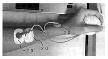
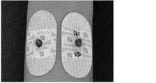
- the figure of the photograph which shows the state which adhered and attached the biological device of this invention to a human upper arm part.
- the schematic diagram which shows the fabrication of the bioelectrode of low adhesiveness.
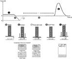
- a schematic diagram showing the state of score evaluation Schematic diagram of adhesiveness evaluation by a tensile tester.
- the photographic figure which shows the state of the measurement of sEMG.
- the figure which shows the result of the fluorescence observation of the polymer thin film attached to the bioelectrode.
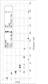
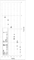
- the figure which shows the correlation between the film thickness and the adhesiveness score The figure which shows the correlation between the film thickness of a polymer thin film, and the adhesive force in a biological device using Vitrod (registered trademark) F-150M as a biological electrode.
- the figure which shows the result of having observed the sEMG signal of Example 1 (the SBS film of 110 nm thickness was attached to the adhesive gel layer).
- the figure which shows the result of having observed the sEMG signal of Example 5 (the SBS film of 1770 nm thickness was attached to the adhesive gel layer).
- the figure which shows the result of having observed the sEMG signal of Example 6 (the PDMS film of 160 nm thickness was attached to the adhesive gel layer).
- the figure which shows the result of having observed the sEMG signal of Example 9 (the PDMS film of 1060 nm thickness was attached to the adhesive gel layer).
- the figure which shows the result of having observed the sEMG signal of Example 10 (the PS film of 120 nm thickness was attached to the adhesive gel layer).
- the figure which shows the result of having observed the sEMG signal of Example 13 (the PS film of 500 nm thickness was attached to the adhesive gel layer).
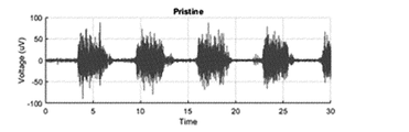
- the figure which shows the result of observing the sEMG signal of a positive control group (without affixing a polymer thin film).
- the figure which shows the result of having observed the sEMG signal of Example 17 (the PLA film of 160 nm thickness was attached to the adhesive gel layer).
- the figure which shows the result of having observed the sEMG signal of Example 18 (the porous thin film of 140 nm thickness was attached to the adhesive gel layer).
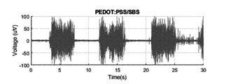
- the figure which shows the result of having observed the sEMG signal of Example 19 (the polymer thin film which laminated the PEDOT / PSS film and the SBS film was attached to the adhesive gel layer).
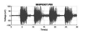
- the figure which shows the result of having observed the sEMG signal of Example 20 (a polymer thin film which laminated SBS film and PEDOT / PSS film was attached to the adhesive gel layer).
- One of the embodiments of the present invention is a biological device. More specifically, it is a low-adhesive biological device having reduced adhesiveness to a biological part to be adhered, wherein the biological device includes an electrode portion, an adhesive gel layer adhered to an electrode surface of the electrode portion, and the like. It has a polymer thin film laminated on the surface of the adhesive gel layer, and while maintaining the ability to exchange electrical signals with the living body, the adhesiveness to the living body is reduced by the adhesive strength of the adhesive gel layer. It is a biological device having.
- the electrode portion refers to an electrode portion for transmitting and receiving an electric signal in the biological device of the present invention.
- the electrode is not limited to the electrode portion that receives an electrical signal from the living body or gives an electrical stimulus to the living body, and the electrode is a biological component intended for measurement.
- the electrode is used as an electrode unit in combination with various sensor units, and includes an electrode for measuring a change in an electric signal caused by sensing a biological component to be measured.
- Examples of the biological device of the present invention include a biological electrode, a glucose sensor, a pH sensor, an ion sensor, a gas sensor, a thermometer, an acceleration sensor, a strain sensor and the like. These biological devices can be used for various devices such as electroencephalographs, electromyograms, electrocardiographs, and electrical stimulators.
- Conventional products of these biological devices have an adhesive gel layer on the electrode portion and the electrode surface of the electrode portion, and are used by adhering to an organ such as skin, and direct or indirect electricity with the living body. Signals are sent and received.
- the conventional product of this biological device has a strong adhesive force to the skin or the like of the adhesive gel, and may cause skin disorders including inflammation such as redness or rash, which has been a problem.
- a polymer thin film is attached to the surface of the adhesive gel layer using a commercially available biological electrode or various sensors, and the adhesive gel layer and the polymer thin film are laminated. Therefore, it can be manufactured as a biological device having reduced adhesiveness to skin and the like.
- the biological device of the present invention retains the transfer of electrical signals to and from the living body and the measurement of electrical signals changed by various sensors, while providing the adhesive force to the living body, which is less than the adhesive strength of the adhesive gel layer.
- the polymer thin film used in the biological device of the present invention does not necessarily have adhesive strength by itself. However, even when the polymer thin film itself does not have adhesive strength, the adhesiveness is reduced by laminating the polymer thin film on the surface of the adhesive gel layer, but the surface of the polymer film is applied to organs such as skin.
- the present inventors have discovered that they have adhesiveness and can exchange electrical signals with living organisms. The present invention is based on this finding.
- the biological device of the present invention can be used without causing deviation with respect to the target site by adhering the polymer thin film surface to the skin or the like of the living body. At this time, the ability to send and receive electric signals can be maintained through the polymer thin film.
- the material of the polymer thin film used in the biological device of the present invention is not particularly limited as long as it is a polymer thin film, and includes non-conductive polymers and conductive polymers. Further, it may be an elastomer or a hard polymer thin film. Further, a plurality of polymers may be contained in the polymer thin film. Typical examples of the material of this polymer thin film are polystyrene-block-polybutadiene-block-polystyrene (SBS), polydimethylsiloxane (PDMS), polystyrene (PS), poly-L-lactic acid (PLLA), and poly-D-.
- SBS polystyrene-block-polybutadiene-block-polystyrene
- PDMS polydimethylsiloxane
- PS polystyrene
- PLLA poly-L-lactic acid
- poly-D- poly-D-.
- Lactic acid (PDLA), poly-D, L-lactic acid (PDLLA), polycaprolactone (PCL), polyglycolic acid (PLGA), polylactic acid-glycolic acid copolymer (PLGA), chitosan, alginic acid, poly (4-styrene).
- Polystyrene (3,4-ethylenedioxythiophene) (PEDOT: PSS) doped with (styrene acid) can be mentioned.
- the polymer thin film may be a polymer thin film made of a material obtained by combining and mixing materials of the various materials.
- a polymer thin film prepared by using a material obtained by combining polylactic acid and polystyrene and mixing them the polymer thin film becomes porous, so that when it is used as a biological device, it does not depend on an adhesive gel. Since the adhesiveness to the skin is improved, good electrode characteristics can be maintained (see Example 18).
- the composition of the polymer thin film used in the biological device of the present invention may be a plurality of layers as long as it acts as a biological device.
- the materials described in the material of the polymer thin film can be used in combination.
- the conductivity is improved as compared with the case where the polymer thin film is formed by SBS alone. It is possible to maintain good electrode characteristics (see Examples 19 and 20).
- the polymer thin film used in the biological device of the present invention can contain additives as long as it acts as a biological device.
- the amount of the additive is preferably in the range of 0 to 5% by mass with respect to the total mass of the polymer thin film phase.
- Known additives include, for example, antioxidants, weathering stabilizers, heat stabilizers, lubricants, crystal nucleating agents, UV absorbers, colorants, surfactants and the like.
- a plurality of types of additives may be contained.
- particles made of an inorganic or organic compound may be contained. The amount of particles is preferably in the range of 0 to 5% by mass with respect to the total mass of the adhesion prevention layer.
- Examples of known particles include particles made of calcium carbonate, titanium dioxide, silicon dioxide, calcium fluoride, lithium fluoride, alumina, barium sulfate, zirconia, calcium phosphate and the like, crosslinked polystyrene particles, metal nanoparticles and the like. Be done.
- the film formation of the polymer thin film used for manufacturing the biological device of the present invention can be performed by using a known film formation method such as a roll-to-roll method using a gravure coater.
- a gravure coater is used to coat, for example, a polyethylene terephthalate (PET) film with an aqueous solution of a sacrificial first layer of polyvinyl alcohol (PVA) and then dried to form a PVA layer.
- PVA polyvinyl alcohol
- the PVA layer is coated with a solution of the polymer thin film material constituting the biological device of the present invention, for example, a tetrahydrofuran solution of SBS, dried, and the second layer is laminated.
- a laminated film in which the first layer and the second layer are laminated is produced.
- a paper tape is attached to the surface on which the second layer is formed so as to border the required shape, and the two-layer film including the first layer and the second layer is peeled off from the edge. It is peeled off from the PET film while being held in place.
- the paper tape holding the SBS polymer thin film is cut out into a desired shape and used, and the polymer thin film of the second layer is laminated on the adhesive gel layer of the biological device to form the second layer on the adhesive gel layer. It is possible to manufacture a biological device in which a polymer thin film is laminated.
- the size of the polymer thin film used in the biodevice of the present invention may be such that the adhesive gel layer contained in the bioelectrode or various sensors is sufficiently covered, and the polymer thin film may be larger than the adhesive gel layer. No (Fig. 1).
- the biological device of the present invention only needs to have the adhesive gel layer in sufficient contact with the polymer thin film, and can be configured differently depending on the application. That is, the adhesive gel layer contained in the bioelectrode or various sensors may be coated with a polymer thin film in advance to prepare a low-adhesive biological device, and then adhered to a target site such as skin in advance.
- a structure of a low-adhesive biodevice may be provided by adhering a bioelectrode or various sensors on the polymer thin film after the polymer thin film is attached to the polymer thin film.
- An example of the film thickness of the polymer thin film in the biological device of the present invention is 50 to 2000 nm, preferably 50 to 1000 nm, and more preferably 100 to 500 nm.
- the ratio of the adhesive force of the biological device to the living body to the adhesive force of the adhesive gel layer to the living body is 10 to 90%, preferably 20 to 80%, and more preferably 30 to 70%.
- the biological device of the present invention can reduce the adhesive force of the adhesive gel and prevent or reduce the skin damage caused by the adhesive gel layer by laminating a polymer thin film on the surface of the adhesive gel layer.
- polymer thin film Another embodiment of the present invention is a polymer thin film. More specifically, it is a polymer thin film laminated on the surface of the adhesive gel layer of the biological device described in the above "1. Biodevice", and is an adhesive gel of the biological device while retaining the exchange of electrical signals. It is a polymer thin film for reducing the adhesiveness of the material.
- the polymer thin film of the present invention is a polymer thin film constituting the biological device described in the above "1. Biological device”.
- the polymer thin film of the present invention can be manufactured and used by the manufacturing method described in the above section "1. Biological device”.
- An example of the film thickness of the polymer thin film in the polymer thin film of the present invention is 50 to 2000 nm, preferably 50 to 1000 nm, and more preferably 100 to 500 nm.
- the ratio of the adhesive force of the biological device to the living body to the adhesive force of the adhesive gel layer to the living body is preferably 10 to 90%. It is 20 to 80%, more preferably 30 to 70%.
- the polymer thin film of the present invention is a polymer for reducing the adhesion of various devices such as bioelectrodes, glucose sensors, pH sensors, ion sensors, gas sensors, thermometers, acceleration sensors, and strain sensors to organs such as skin. Can be used as a thin film.
- the polymer thin film of the present invention it is possible to reduce the adhesive force of the adhesive gel in the biological device and prevent or reduce the skin damage caused by the adhesive gel layer.
- Another embodiment of the present invention is the method for reducing the adhesiveness of biological devices described in the above "1. Biological device”. More specifically, in the above-mentioned biological device, it is a method of reducing the adhesiveness of the adhesive gel of the biological device to the living body while maintaining the exchange of electric signals by laminating the polymer thin film.
- examples of the film thickness of the polymer thin film include 50 to 2000 nm, preferably 50 to 1000 nm, and more preferably 100 to 500 nm.
- the ratio of the adhesive force of the biological device to the living body to the adhesive force of the adhesive gel layer to the living body is 10 to 90%, preferably 20. It is -80%, more preferably 30-70%.
- bioelectrodes glucose sensors
- pH sensors pH sensors
- ion sensors gas sensors
- thermometers thermometers
- accelerometers and strain sensors that reduce the adhesive force of the adhesive gel in the biodevices.
- the method of the present invention it is possible to reduce the adhesive force of the adhesive gel in the biological device and prevent or reduce the skin damage caused by the adhesive gel layer.
- the polymer thin film was formed based on the gravure printing method (hereinafter referred to as the gravure method). More specifically, on a PET film, a polystyrene-block-polybutadiene-block-polystyrene (SBS) polymer thin film (Examples 1 to 5 and Examples 14) and a polydimethylsiloxane (PDMS) polymer thin film (PDMS) Examples 6-9 and 15), polystyrene (PS) polymer thin films (Examples 10-13 and 16), polylactic acid (PLA) polymer thin films (Example 17), porous (Porous).
- SBS polystyrene-block-polybutadiene-block-polystyrene
- PDMS polydimethylsiloxane
- PS polystyrene
- PS polymer thin films
- PLA polylactic acid
- porous Porous
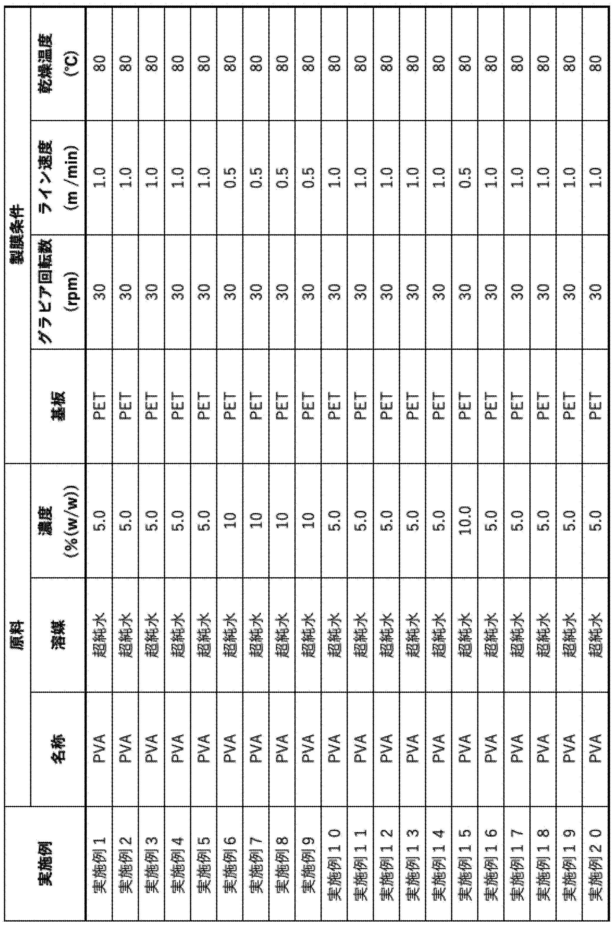
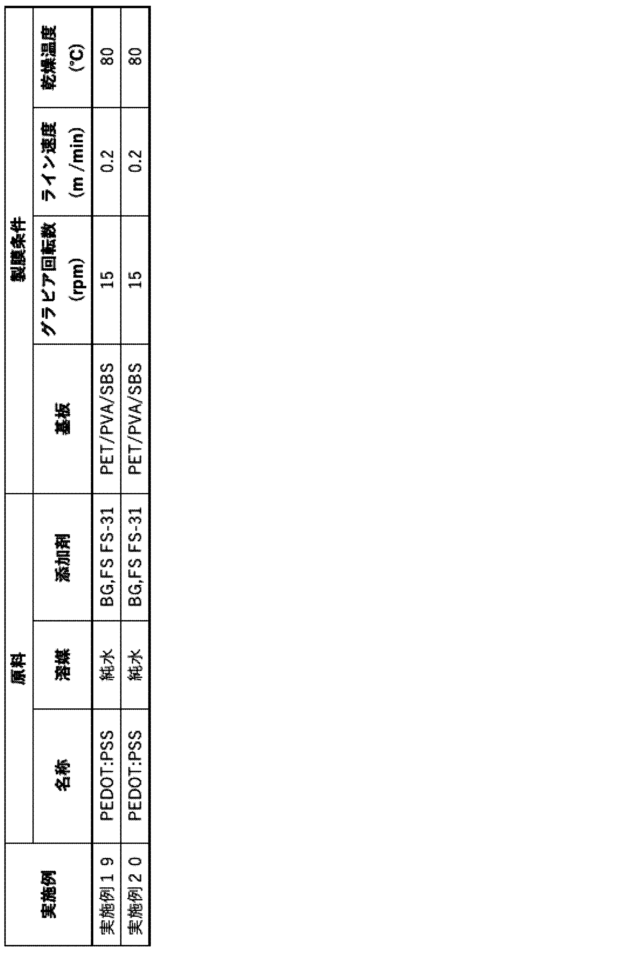
- Table 1 below describes the details of the preparation conditions for the first layer, Table 2 for the second layer, and Table 3 for the third layer.
- a release layer of the first layer was formed.
- polyvinyl alcohol Poly vinyl alcohol: PVA, manufactured by Kanto Chemical Co., Inc., Mw 22,000, hydrolysis rate 86.5 to 89%) was used. PVA was adjusted to 5.0% (w / w) using pure water as a solvent, and a film was formed at a gravure rotation speed of 30 rpm, a line speed of 1.0 m / min, and a drying temperature of 80 ° C.
- Table 1 shows the preparation conditions for the first layer.
- a second polymer thin film layer was formed.
- Polystyrene-block-polybutadiene-block-polystyrene (Polystyrene-block-polybutadie-block-polystyrene style: SBS, manufactured by Sigma-Aldrich, Mw 140,000, 30% styrene block) was used as the raw material for the second layer. .. Tetrahydrofuran (THF, manufactured by Wako Pure Chemical Industries, Ltd., special grade reagent) was used as a solvent, and the concentration was adjusted to various concentrations (2,3,10,20% (w / w)).
- Each of the prepared solutions was formed on the first PVA layer at a gravure rotation speed of 10 to 50 rpm, a line speed of 0.4 to 1.3 m / min, and a drying temperature of 40 ° C., and made of SBS having different film thicknesses.
- a polymer thin film was prepared. Table 2 shows the preparation conditions for the second layer.
- a paper tape (3M Co., Ltd., masking tape 243J Plus 243J15) is attached to the surface on which the polymer thin film is formed so as to border the required shape, and peeled off from the edges to form the first layer and the second layer.
- the two-layer film containing the above was peeled off from the PET film while being held on the paper tape.
- a second polymer thin film layer was formed.
- polydimethylsiloxane Polydimethicyl siloxane: PDMS, SYLGARD (registered trademark) 184 Silicone Elastomer, manufactured by Dow Corning Co., Ltd.
- Hexane manufactured by Fujifilm Wako Pure Chemical Industries, Ltd., special grade reagent
- ethyl acetate manufactured by Fujifilm Wako Pure Chemical Industries, Ltd., special grade reagent
- the PDMS solution was adjusted to various concentrations using a mixed solvent (10,15% (w / w)).
- a mixed solvent (10,15% (w / w)
- Each of the prepared solutions was formed on the first PVA layer at a gravure rotation speed of 20 to 50 rpm, a line speed of 0.2 m / min, and a drying temperature of 80 ° C.
- the formed film was fired in a drying oven at 80 ° C. for 12 hours to prepare PDMS polymer thin films having different film thicknesses.
- Table 2 shows the preparation conditions for the second layer.
- a second polymer thin film layer was formed.
- polystyrene Polystyrene: PS, manufactured by Sigma-Aldrich, Mw 280,000
- Ethyl acetate manufactured by Wako Pure Chemical Industries, Ltd., special grade reagent
- concentration was adjusted to various levels (2.5% (w / w)).
- Each of the prepared solutions was formed on the first PVA layer at a gravure rotation speed of 20 to 40 rpm, a line speed of 1.0 to 1.3 m / min, and a drying temperature of 60 ° C., and made of PS having different film thicknesses.
- a polymer thin film was prepared. Table 2 shows the preparation conditions for the second layer.
- a second polymer thin film layer was formed.
- polylactic acid Polylactic acid: PLA, manufactured by Polysciences Inc., Mw 300,000-600,000
- concentration was adjusted to 2.0% (w / w) using ethyl acetate (manufactured by Wako Pure Chemical Industries, Ltd., special grade reagent) as a solvent.
- the prepared solution was formed on the first PVA layer at a gravure rotation speed of 30 rpm, a line speed of 1.3 m / min, and a drying temperature of 60 ° C. Table 2 shows the preparation conditions for the second layer.
- a second polymer thin film layer was formed.
- polylactic acid Polylactic acid: PLA, Polysciences Inc., Mw 300,000-600,000
- polystyrene Polystylerene: PS, Sigma-Aldrich, Mw 280,000
- PLA ethyl acetate
- PS ethyl acetate
- a porous polymer thin film made of PLA was prepared by immersing a blend membrane having a phase-separated structure of PLA and PS in cyclohexane (manufactured by Kanto Chemical Co., Inc.) and selectively dissolving the PS phase.
- Table 2 shows the preparation conditions for the second layer.
- PEDOT PSS dispersion (manufactured by Heraeus, Clevios PH100) as the raw material for the third layer, and butanediol (1,4-Butanediol: BG, manufactured by Fujifilm Wako Pure Chemical Industries, Ltd.) as an additive, 5% ( w / w) and FS-31 (Capstone FS-31 manufactured by Sigma-Aldrich) were used.
- BG was added to the PEDOT: PSS dispersion at a concentration of 5% (w / w) and FS-31 was added at a concentration of 1% (v / v).
- the prepared solution was formed on the PVA of the first layer and the SBS of the second layer at a gravure rotation speed of 15 rpm, a line speed of 0.2 m / min, and a drying temperature of 80 ° C. to prepare a PEDOT: PSS polymer thin film. did.
- Table 3 shows the preparation conditions for the third layer.
- a natural convection low-temperature dryer (SONW-300S-R, manufactured by AS ONE) was used to heat-treat at 140 degrees for 15 minutes to prepare a PEDOT: PSS polymer thin film.
- Example 19 the third PEDOT: PSS layer was attached so as to cover the adhesive gel layer of the bioelectrode to prepare a biodevice.
- Example 20 the second SBS layer was attached so as to cover the adhesive gel layer of the bioelectrode to prepare a biodevice.
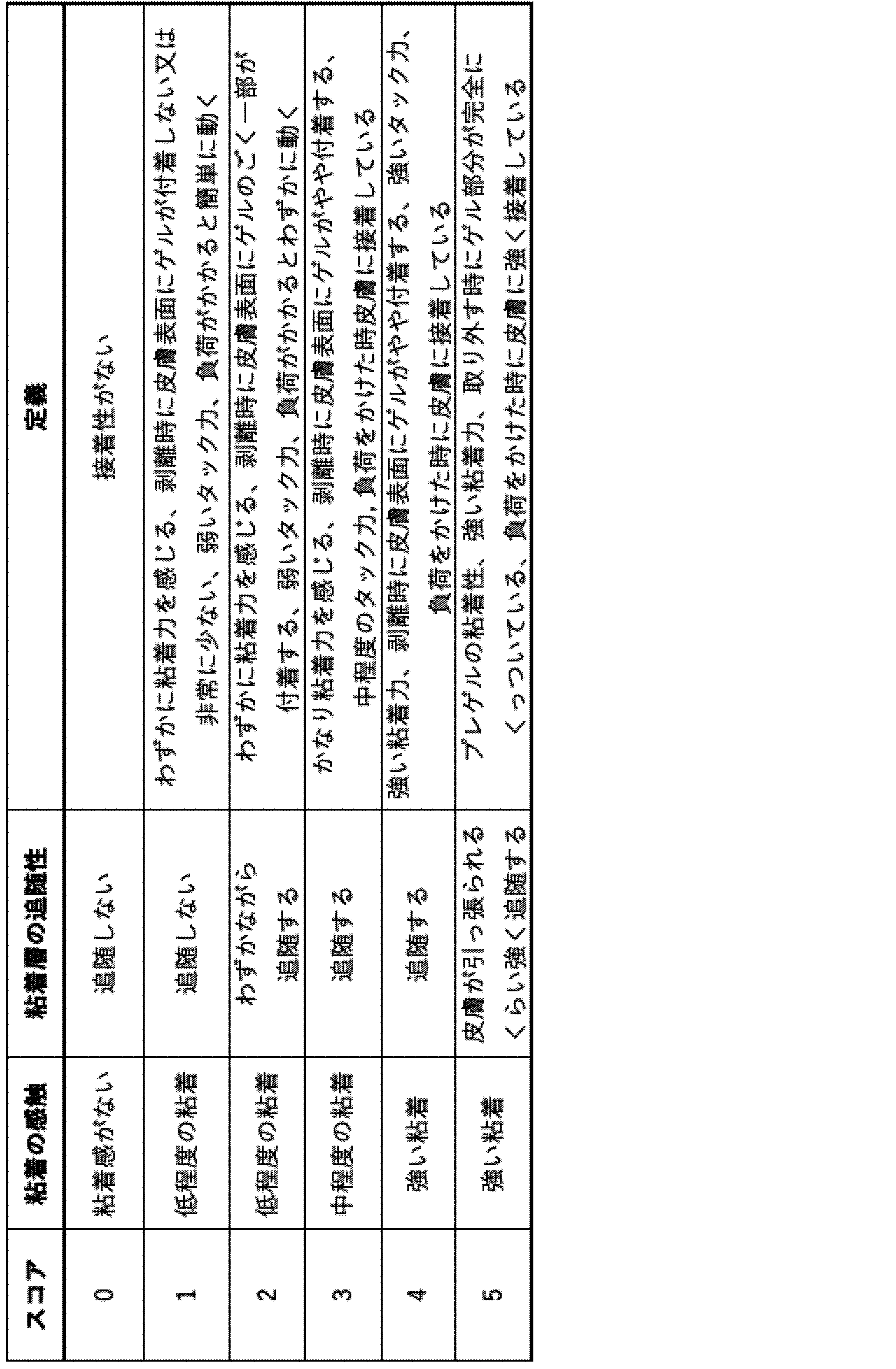
- a score of 0 indicates that there is no adhesiveness, the adhesive layer does not follow, and the adhesiveness is insufficient as a bioelectrode.
- the adhesive feeling is strong, the adhesive layer strongly follows, and it indicates that the bioelectrode has sufficient adhesiveness.
- a positive control group an existing bioelectrode itself to which a polymer thin film was not attached was used, and a qualitative evaluation based on an adhesive score was performed.
- the button portion of the bioelectrode was gripped with a clip on a tensile tester (EZ-SX 5N, manufactured by Shimadzu Corporation) and connected to the load cell.
- An artificial skin (Bioskin plate manufactured by Bulux Co., Ltd.) was placed under the bioelectrode and lowered at 0.5 mm / min to bring it into contact with the artificial skin. It was lowered until a stress of 1 N was applied at a contact area of 1 cm 2, and then increased at 0.5 mm / min until the stress became zero.
- sEMG using a low-adhesive bioelectrode was measured (Fig. 4). Specifically, the measurement was performed under the conditions of a sampling rate of 1,000 Hz and a power line filter of 50 Hz. In addition, two electrodes were mounted at a position 10 cm distal to the elbow on the dominant arm side so that the distance between the electrodes was 2 cm. In addition, it touched the ground at the position of the wrist. The operation of grasping the baseball ball for 3 seconds and then performing for 3 seconds was performed for 5 cycles, and the sEMG signal was measured. As the positive control group, the existing bioelectrode itself to which the polymer thin film was not attached was used.
- SNR signal-to-noise ratio
- SNR was calculated from the signal diagram obtained in 1) according to the following (Equation 1).
- SNR (db) 20log 10 ( A s / A n) ( Equation 1)
- a s is the maximum value of the signal obtained in time in which focus
- a n denotes the standard deviation of the background signal obtained in the time that does not focus.
- the electrode performance of the low-adhesion bioelectrode was evaluated by using the SNR value and comparing it with the value of the positive control group.
- the film thickness of the polymer thin film decreased, the SNR value increased and it was possible to acquire the myoelectric signal more easily.
- the film thickness of less than 200 nm was only about 10% different from that of the positive control group, and the characteristics as an electrode could be maintained (FIGS. 10 to 20).
- the low-adhesive bioelectrode using the two-layer film of PEDOT: PSS and SBS as the polymer thin film was compared with the low-adhesion bioelectrode using the polymer thin film of another material. It was shown that the characteristics as an electrode were better maintained (FIGS. 19 and 20).
- the existing bioelectrode (Nihon Kohden, Vitrode (registered trademark) F150M) itself, which does not have a polymer thin film attached, is attached to the inside of the upper arm and then removed. The degree of inflammatory symptoms at the site of application was observed.
- -Positive control group Commercially available bioelectrode (Nihon Kohden, Vitrode (registered trademark) F150M)
- SBS A low-adhesive biological device using the polymer thin film of Example 1 c.
- PDMS Low-adhesive biological device using the polymer thin film of Example 6-PS: Low-adhesive biological device using the polymer thin film of Example 10-PEDOT: PSS / SBS: Polymer thin film of Example 19. Low-adhesive biological device using the
- FIGS. 21A and 21A show photographs showing the state before, during, and immediately after attachment of a commercially available bioelectrode, which is a group of low-adhesive biological devices or a positive control group, after being attached and removed for 2 hours, respectively.
- 21B shown in FIG. 21C.
- the low-adhesive device of the present invention suppresses the induction of adverse events such as skin inflammation and is useful.
- the biological device of the present invention is used for diagnosis and / or treatment of diseases by adhering to organs such as skin as a biological electrode, glucose sensor, pH sensor, ion sensor, gas sensor, thermometer, acceleration sensor, strain sensor and the like.
- organs such as skin as a biological electrode, glucose sensor, pH sensor, ion sensor, gas sensor, thermometer, acceleration sensor, strain sensor and the like.
- These biological devices can be used for various devices such as electroencephalographs, electromyograms, electrocardiographs, and electrical stimulators.
- Bioelectrode 2 Polymer thin film attached to the skin 11: Polymer thin film 12: Adhesive layer 13: Base material 14: Electrode 20: Low adhesive bioelectrode 30: Skin
Landscapes
- Health & Medical Sciences (AREA)
- Life Sciences & Earth Sciences (AREA)
- Animal Behavior & Ethology (AREA)
- Veterinary Medicine (AREA)
- Public Health (AREA)
- Engineering & Computer Science (AREA)
- Biomedical Technology (AREA)
- General Health & Medical Sciences (AREA)
- Pathology (AREA)
- Molecular Biology (AREA)
- Surgery (AREA)
- Medical Informatics (AREA)
- Heart & Thoracic Surgery (AREA)
- Physics & Mathematics (AREA)
- Biophysics (AREA)
- Nuclear Medicine, Radiotherapy & Molecular Imaging (AREA)
- Radiology & Medical Imaging (AREA)
- Laminated Bodies (AREA)
- Medicinal Preparation (AREA)
Abstract
従来の生体電極等の生体デバイスは、高すぎる粘着ゲル層の接着性が問題であった。本発明は、接着する生体部位に対する接着性が低減された低接着性の生体デバイスであって、該生体デバイスは、電極部と、電極部の電極面に接着された粘着ゲル層と、該粘着ゲル層の表面に積層された高分子薄膜とを有し、生体との間で電気信号の授受能力を保持しつつ、前記粘着ゲル層の接着力よりも低減された生体への接着性を有する生体デバイスを提供する。また、生体デバイスの粘着ゲルの接着性を低減するための高分子薄膜、及び、電気信号の授受を保持しつつ生体デバイスの粘着ゲルの生体に対する接着性を低減させる方法を提供する。
Description
本発明は、低接着性の生体デバイス、該生体デバイスの粘着ゲルの接着性を低減するための高分子薄膜、及び、前記生体デバイスの粘着ゲルの接着性を低減させる方法に関する。
筋電図(Electromyogram:EMG)、心電図(Electrocardiogram:ECG)、脳波(Electroencephalogram:EEG)などの生体信号は身体の電気信号(以下、生体信号と略す)を測定、及び、観測する用途として、汎用的に用いられる指標である。これらの生体信号を計測するために、生体電極が用いられる。
また、例えば、筋肉痛や肩こり等に対して行われる電気治療においても、患部に貼付して生体電極が用いられる。
さらに、生体電極、グルコースセンサー、pHセンサー、イオンセンサー、ガスセンサー、体温計、加速度センサー及びひずみセンサーにおいても、その構成部材として電極部を有し、該電極部を粘着ゲルによって皮膚等に接着して使用されている(非特許文献1)。
これらの生体デバイスは、生体からの微弱な電気信号若しくは対象物質の検知によって惹起される微弱な電気信号を正確に検知するために、又は、電気治療を行う患者の患部に正確に電気刺激を与えるために、ずれがでないよう測定部位に対して強固に接着する必要がある。従来商品化されている生体電極については、生体信号等の電気信号の検知や授受と強固な接着の両方を達成するために、導電性の粘着ゲルが用いられている(例えば、アクリル系親水性高分子)。これにより強固な接着性を達成する一方、従来品は接着性が高すぎるため、測定部下の皮膚から剥がす際には刺激が強く、また、長期での使用ではかゆみや発赤を伴う炎症等の皮膚障害を生じる場合があった(非特許文献2、非特許文献3)。
Heikenfeld,J. et al., Lab Chip,18,217(2018).
Dervisevic,M. et al., Nano Today,30,100828(2020).
Lien,M. et al., Contact Dermatitis,79,81(2018).
従来の生体電極等の生体デバイスは、高すぎる粘着ゲル層の接着性が問題であった。本発明は、接着性を低減できるだけでなく、電極としての電気信号の授受能力も維持できる低接着性の生体デバイスを提供することを課題とする。
本発明者らは、低接着性の生体デバイスを開発した。具体的には、生体電極等の生体デバイスの粘着ゲル上に、高分子材料を原料とした厚さ数十~2000nmからなる高分子薄膜を貼付し、粘着ゲルの接着性を低下させつつも、生体信号の授受が可能な新規な電極構成を提案し、検証を行い、本発明を完成させた。
より具体的には、本発明は、接着する生体部位に対する接着性が低減された低接着性の生体デバイスであって、該生体デバイスは、電極部と、電極部の電極面に接着された粘着ゲル層と、該粘着ゲル層の表面に積層された高分子薄膜とを有し、生体との間で電気信号の授受能力を保持しつつ、前記粘着ゲル層の接着力よりも低減された生体への接着性を有する生体デバイスを提供する。
本発明の生体デバイスにおいて、前記高分子薄膜が、複数層で形成されている場合がある。
本発明の生体デバイスにおいて、前記高分子薄膜の膜厚が50~2000nmである場合がある。
本発明の生体デバイスにおいて、前記粘着ゲル層の生体への接着力に対して、前記生体デバイスの生体への接着力の割合が、10~90%である場合がある。
本発明の生体デバイスにおいて、前記生体デバイスが、生体電極、グルコースセンサー、pHセンサー、イオンセンサー、ガスセンサー、体温計、加速度センサー又はひずみセンサーから選択される場合がある。
本発明の生体デバイスは、前記粘着ゲル層によって惹起される皮膚障害を予防又は軽減するための生体デバイスである場合がある。
また、本発明は、前記生体デバイスの粘着ゲル層の表面に積層された高分子薄膜であって、電気信号の授受を保持しつつ、生体デバイスの粘着ゲルの接着性を低減するための高分子薄膜を提供する。
本発明の高分子薄膜において、該高分子薄膜が複数層で形成されている場合がある。
本発明の高分子薄膜において、前記高分子薄膜の膜厚が50~2000nmである場合がある。
本発明の高分子薄膜において、前記粘着ゲル層の接着力に対して、前記生体デバイスの接着力の割合が、10~90%である場合がある。
本発明の高分子薄膜において、前記生体デバイスが、生体電極、グルコースセンサー、pHセンサー、イオンセンサー、ガスセンサー、体温計、加速度センサー又はひずみセンサーから選択される場合がある。
本発明の高分子薄膜は、前記粘着ゲル層によって惹起される皮膚障害を予防又は軽減するための高分子薄膜である場合がある。
さらに、本発明は、前記生体デバイスにおいて、高分子薄膜を積層することによる、電気信号の授受を保持しつつ生体デバイスの粘着ゲルの生体に対する接着性を低減させる方法を提供する。
本発明の方法において、前記高分子薄膜が複数層で形成されている場合がある。
本発明の方法において、前記高分子薄膜の膜厚が50~2000nmである場合がある。
本発明の方法において、前記粘着ゲル層の接着力に対して、前記生体電極の接着力の割合が、10~90%である場合がある。
本発明の方法において、前記生体デバイスが、生体電極、グルコースセンサー、pHセンサー、イオンセンサー、ガスセンサー、体温計、加速度センサー又はひずみセンサーから選択される場合がある。
本発明の方法は、前記粘着ゲル層によって惹起される皮膚障害を予防又は軽減するための方法である場合がある。
本発明では、厚さが数十~2000nmからなる高分子薄膜を生体デバイスの粘着ゲル層に積層することで、接着性を低減できるだけでなく、電極としての能力も維持できる。
1.生体デバイス
本発明の実施形態の1つは、生体デバイスである。より具体的には、接着する生体部位に対する接着性が低減された低接着性の生体デバイスであって、該生体デバイスは、電極部と、電極部の電極面に接着された粘着ゲル層と、該粘着ゲル層の表面に積層された高分子薄膜とを有し、生体との間で電気信号の授受能力を保持しつつ、前記粘着ゲル層の接着力よりも低減された生体への接着性を有する生体デバイスである。
本発明の実施形態の1つは、生体デバイスである。より具体的には、接着する生体部位に対する接着性が低減された低接着性の生体デバイスであって、該生体デバイスは、電極部と、電極部の電極面に接着された粘着ゲル層と、該粘着ゲル層の表面に積層された高分子薄膜とを有し、生体との間で電気信号の授受能力を保持しつつ、前記粘着ゲル層の接着力よりも低減された生体への接着性を有する生体デバイスである。
本明細書において、電極部は、本発明の生体デバイスにおいて電気信号を授受するための電極部分を言う。
本明細書において、電極は、生体からの電気的な信号を受信する、或いは、生体に対して電気刺激を与える電極部分に限定されるものではなく、電極は、測定を目的とする生体由来成分に対する各種センサーデバイスにおいて、各種センサー部と組み合わせて電極部として用いられ、測定対象の生体由来成分の感知によって生じる電気信号の変化を測定するための電極を含む。
本発明の生体デバイスの例としては、生体電極、グルコースセンサー、pHセンサー、イオンセンサー、ガスセンサー、体温計、加速度センサー、及びひずみセンサー等が挙げられる。これらの生体デバイスは、脳波計、筋電計、心電計、電気刺激装置をはじめとした各種デバイスに使用できる。
これらの生体デバイスの従来品は、電極部と、該電極部の電極表面に粘着ゲル層を有し、皮膚等の臓器に接着して使用され、生体との間で直接的又は間接的な電気信号の授受が行われる。
そして、これらの生体デバイスは、電極部の電極表面に粘着ゲルが接着されたデバイスが商業的に利用可能である。しかし、この生体デバイスの従来品は、粘着ゲルの皮膚等への粘着力が強力であり、発赤又はかぶれ等の炎症を含む皮膚障害を惹起する場合があり、問題となっていた。
そこで、本発明の生体デバイスは、商業的に利用可能な生体電極や各種センサーを使用して、粘着ゲル層の表面に高分子薄膜を貼付し、粘着ゲル層と高分子薄膜とを積層することによって、皮膚等に対する接着性を低減した生体デバイスとして製造できる。これにより、本発明の生体デバイスは、生体との電気信号の授受や各種センサーによって変化する電気信号の測定を保持しつつ、前記粘着ゲル層の接着力よりも低減された生体への接着性を有する。
本発明の生体デバイスで用いられる前記高分子薄膜は、それ自体が粘着力を有するとは限らない。しかし、高分子薄膜自体が粘着力を有しない場合であっても、高分子薄膜を粘着ゲル層の表面に積層することにより接着性が低減されるものの高分子膜表面は皮膚等の臓器に対して接着性を有し、かつ、生体と電気信号を授受できることを本発明者らは発見した。本発明はこの発見に基づく。
本発明の生体デバイスは、高分子薄膜面を生体の皮膚等に接着することにより、標的部位に対してずれを生じることなく使用することができる。このとき、高分子薄膜を介して電気信号の授受能力が保持できる。
本発明の生体デバイスで使用される高分子薄膜の材質は、高分子薄膜である限り特に限定されず、非導電性ポリマーや導電性ポリマーが含まれる。また、エラストマーや硬質系の高分子薄膜であってもよい。更に、高分子薄膜中に複数の高分子が含まれていても構わない。この高分子薄膜の材質の典型例としては、ポリスチレン-block-ポリブタジエン-block-ポリスチレン(SBS)、ポリジメチルシロキサン(PDMS)、ポリスチレン(PS)、ポリ―L―乳酸(PLLA)、ポリ―D―乳酸(PDLA)、ポリ―D,L―乳酸(PDLLA)、ポリカプロラクトン(PCL)、ポリグリコール酸(PLGA)、ポリ乳酸―グリコール酸共重合体(PLGA)、キトサン、アルギン酸、ポリ(4-スチレンスルホン酸)をドープしたポリ(3,4-エチレンジオキシチオフェン)(PEDOT:PSS)などが挙げられる。
前記高分子薄膜は、前記各種材質の材料を組み合わせて混合した材料で作製した高分子薄膜であってもよい。例えば、ポリ乳酸とポリスチレンとを組み合わせてこれらを混合した材料を用いて作製した高分子薄膜の場合、高分子薄膜が多孔性になるため、生体デバイスとした場合に、粘着性ゲルによることなく、皮膚との接着性が向上するため良好な電極特性を維持することができる(実施例18参照)。
本発明の生体デバイスで使用される高分子薄膜の構成は、生体デバイスとして作用する限り2層以上の複数層であっても構わない。各層の構成要素については、例えば前記高分子薄膜の材質に記される材料を組み合わせて使用することができる。例えば、SBSからなる高分子薄膜とPEDOT:PSSからなる導電性薄膜とを組み合わせた複数層として高分子薄膜を形成すると、SBS単独で高分子薄膜が形成されている場合よりも、導電性を向上させ、良好な電極特性を維持することができる(実施例19及び20参照)。
本発明の生体デバイスで使用される高分子薄膜には、生体デバイスとして作用する限り添加剤を含有することができる。添加剤の量は、高分子薄膜相の全質量に対して0~5質量%の範囲であることが好ましい。公知の添加剤としては、例えば、酸化防止剤、耐候安定剤、熱安定化剤、滑剤、結晶核剤、紫外線吸収剤、着色剤、界面活性剤などが挙げられる。添加剤は複数種含まれていてもよい。また、上述の添加剤とは別に、無機又は有機化合物からなる粒子が含まれていてもよい。粒子の量は、癒着防止層の全質量に対して0~5質量%の範囲であることが好ましい。公知の粒子としては、例えば、炭酸カルシウム、二酸化チタン、二酸化ケイ素、フッ化カルシウム、フッ化リチウム、アルミナ、硫酸バリウム、ジルコニア、及びリン酸カルシウムなどからなる粒子並びに架橋ポリスチレン系粒子、金属ナノ粒子などが挙げられる。
本発明の生体デバイスの製造に使用する高分子薄膜の製膜は、例えば、グラビアコーターを用いたロール・トゥ・ロール法などの公知の製膜方法を用いることによって行うことができる。簡潔には、グラビアコーターを用いて、例えば、ポリエチレンテレフタレート(PET)フィルム上に犠牲層となる第1層目のポリビニルアルコール(PVA)の水溶液を用いてコーティングした後、乾燥してPVA層を製膜する。さらに、このPVA層上に本発明の生体デバイスを構成する高分子薄膜の材料の溶液、例えば、SBSのテトラヒドロフラン溶液を用いてコーティングし乾燥し、第2層目を積層する。これにより、第1層と第2層とが積層した積層膜を作製する。そして、第2層目が製膜された面に例えば紙テープを必要な形状を縁取るように貼付し、縁から剥離することで、第1層と第2層とを含んだ2層膜を紙テープに保持された状態でPETフィルムから剥離する。得られた紙テープにて保持された2層膜を、純水上にPVA面が接するように浮遊させることで、第1層目のPVA層のみを溶解し、紙テープに保持されたSBSの高分子薄膜を得ることができる。このSBS高分子薄膜が保持された紙テープを所望の形に切り出して使用し、第2層目の高分子薄膜を生体デバイスの粘着ゲル層に積層することにより、粘着ゲル層に第2層目の高分子薄膜が積層した生体デバイスを製造できる。
本発明の生体デバイスで使用される高分子薄膜の大きさは、生体電極や各種センサーに含まれる粘着ゲル層が十分に被覆されていればよく、高分子薄膜が粘着ゲル層より大きくても構わない(図1)。
本発明の生体デバイスは、粘着ゲル層が高分子薄膜と十分に接していればよく、用途によって構成を作り分けることができる。すなわち、事前に生体電極や各種センサーに含まれる粘着ゲル層へ高分子薄膜を被覆して低接着性生体デバイスを作製した後に皮膚等の目的部位に接着させてもよく、あらかじめ皮膚等の目的部位に高分子薄膜を貼付した後に該高分子薄膜上に生体電極や各種センサーを接着させることで、低接着性生体デバイスの構成を設けてもよい。
本発明の生体デバイスにおける、前記高分子薄膜の膜厚の例としては、50~2000nm、好ましくは50~1000nm、より好ましくは、100~500nmである。
前記粘着ゲル層の生体への接着力に対する、前記生体デバイスの生体への接着力の割合が、10~90%、好ましくは20~80%、より好ましくは30~70%である。
本発明の生体デバイスは、粘着ゲル層の表面に高分子薄膜を積層することにより、粘着ゲルの接着力を低減し、粘着ゲル層によって惹起される皮膚障害を予防又は軽減することができる。
2.高分子薄膜
本発明のもう1つの実施形態は、高分子薄膜である。より具体的には、上記「1.生体デバイス」に記載された生体デバイスの粘着ゲル層の表面に積層された高分子薄膜であって、電気信号の授受を保持しつつ、生体デバイスの粘着ゲルの接着性を低減するための高分子薄膜である。
本発明のもう1つの実施形態は、高分子薄膜である。より具体的には、上記「1.生体デバイス」に記載された生体デバイスの粘着ゲル層の表面に積層された高分子薄膜であって、電気信号の授受を保持しつつ、生体デバイスの粘着ゲルの接着性を低減するための高分子薄膜である。
本発明の高分子薄膜は、上記「1.生体デバイス」に記載した生体デバイスを構成する高分子薄膜である。
本発明の高分子薄膜は、上記の「1.生体デバイス」の項に記載した製造方法で製造し、使用することができる。
本発明の高分子薄膜における、前記高分子薄膜の膜厚の例としては、50~2000nm、好ましくは50~1000nm、より好ましくは、100~500nmである。
本発明の高分子薄膜を前記生体デバイスに適用して使用したとき、前記粘着ゲル層の生体への接着力に対する、前記生体デバイスの生体への接着力の割合が、10~90%、好ましくは20~80%、より好ましくは30~70%である。
本発明の高分子薄膜は、生体電極、グルコースセンサー、pHセンサー、イオンセンサー、ガスセンサー、体温計、加速度センサー、及びひずみセンサー等の各種デバイスの皮膚等の臓器に対する接着性を低減させるための高分子薄膜として使用できる。
本発明の高分子薄膜を用いることにより、前記生体デバイスにおける粘着ゲルの接着力を低減し、粘着ゲル層によって惹起される皮膚障害を予防又は軽減することができる。
3.生体デバイスの接着性を低減させる方法
本発明のもう1つの実施形態は、上記「1.生体デバイス」に記載された生体デバイスの接着性を低減させる方法である。より具体的には、上記の生体デバイスにおいて、高分子薄膜を積層することによる、電気信号の授受を保持しつつ生体デバイスの粘着ゲルの生体に対する接着性を低減させる方法である。
本発明のもう1つの実施形態は、上記「1.生体デバイス」に記載された生体デバイスの接着性を低減させる方法である。より具体的には、上記の生体デバイスにおいて、高分子薄膜を積層することによる、電気信号の授受を保持しつつ生体デバイスの粘着ゲルの生体に対する接着性を低減させる方法である。
本発明の方法において、前記高分子薄膜の膜厚の例としては、50~2000nm、好ましくは50~1000nm、より好ましくは、100~500nmが挙げられる。
本発明の方法において、前記生体デバイスに適用して使用したとき、前記粘着ゲル層の生体への接着力に対する、前記生体デバイスの生体への接着力の割合が、10~90%、好ましくは20~80%、より好ましくは30~70%である。
本発明の方法を用いることにより、前記生体デバイスにおける粘着ゲルの接着力を低減した生体電極、グルコースセンサー、pHセンサー、イオンセンサー、ガスセンサー、体温計、加速度センサー、及びひずみセンサー等の各種デバイスとして使用できる。
また、本発明の方法を用いることにより、前記生体デバイスにおける粘着ゲルの接着力を低減し、粘着ゲル層によって惹起される皮膚障害を予防又は軽減することができる。
本明細書において言及される全ての文献はその全体が引用により本明細書に取り込まれる。ここに記述される実施例は本発明の実施形態を例示するものであり、本発明の範囲を限定するものとして解釈されるべきではない。
<実験方法>
1.1.高分子薄膜の作製
高分子薄膜は、グラビア印刷法(以下、グラビア法)を基に製膜した。より具体的には、PETフィルム上に、ポリスチレン-block-ポリブタジエン-block-ポリスチレン(SBS)製高分子薄膜(実施例1~5及び実施例14)、ポリジメチルシロキサン(PDMS)製高分子薄膜(実施例6~9及び実施例15)、ポリスチレン(PS)製高分子薄膜(実施例10~13及び実施例16)、ポリ乳酸(PLA)製高分子薄膜(実施例17)、多孔質(Porous)ポリ乳酸(PLA)製高分子薄膜(実施例18)、導電性薄膜(PEDOT:PSS)製高分子薄膜(実施例19及び20)の各種高分子薄膜の原料を溶媒で溶解した溶液を用いて、グラビア法にて製膜し、高分子薄膜が製膜されたPETフィルムをロールトゥロール方式にて巻き取る方法を用いた。
1.1.高分子薄膜の作製
高分子薄膜は、グラビア印刷法(以下、グラビア法)を基に製膜した。より具体的には、PETフィルム上に、ポリスチレン-block-ポリブタジエン-block-ポリスチレン(SBS)製高分子薄膜(実施例1~5及び実施例14)、ポリジメチルシロキサン(PDMS)製高分子薄膜(実施例6~9及び実施例15)、ポリスチレン(PS)製高分子薄膜(実施例10~13及び実施例16)、ポリ乳酸(PLA)製高分子薄膜(実施例17)、多孔質(Porous)ポリ乳酸(PLA)製高分子薄膜(実施例18)、導電性薄膜(PEDOT:PSS)製高分子薄膜(実施例19及び20)の各種高分子薄膜の原料を溶媒で溶解した溶液を用いて、グラビア法にて製膜し、高分子薄膜が製膜されたPETフィルムをロールトゥロール方式にて巻き取る方法を用いた。
以下の表1に第1層の、表2に第2層の、表3に第3層の、それぞれの高分子薄膜の作製条件の詳細を記載した。

1.1.1.ポリスチレン―block-ポリブタジエン―block―ポリスチレン(Polystyrene-block-polybutadiene-block-polystyrene styrene:SBS)製高分子薄膜の作製(実施例1~5)
製膜の事前準備として、PETフィルム(ルミラー(登録商標)、東レ株式会社製、タイプ:T60、厚み25μm)を、グラビア印刷装置(卓上テストコータ ミニラボ(登録商標)、康井精機社製)に通紙した。グラビアロールには、200線の小径グラビアロールを用いた。
製膜の事前準備として、PETフィルム(ルミラー(登録商標)、東レ株式会社製、タイプ:T60、厚み25μm)を、グラビア印刷装置(卓上テストコータ ミニラボ(登録商標)、康井精機社製)に通紙した。グラビアロールには、200線の小径グラビアロールを用いた。
まず、第1層目の剥離層を製膜した。第1層目の原料として、ポリビニルアルコール(Poly vinyl alcohol:PVA、関東化学社製、Mw 22,000、加水分解率86.5~89%)を用いた。純水を溶媒として、PVAを5.0%(w/w)に調整し、グラビア回転数30rpm、ライン速度1.0m/min、乾燥温度80℃で製膜した。第1層目の作製条件を表1に示した。
次いで第2層目の高分子薄膜層を製膜した。第2層目の原料として、ポリスチレン―block―ポリブタジエン―block-ポリスチレン(Polystyrene-block-polybutadiene-block-polystyrene styrene:SBS、Sigma-Aldrich社製、Mw 140,000、30%スチレンブロック)を用いた。テトラヒドロフラン(Tetrahydrofuran:THF、富士フイルム和光純薬株式会社製、試薬特級)を溶媒として、各種濃度に調整した(2,3,10,20%(w/w))。調整した各溶液をそれぞれ第1層目のPVA層上に、グラビア回転数10~50rpm、ライン速度0.4~1.3m/min、乾燥温度40℃で製膜し、膜厚の異なるSBS製高分子薄膜を作製した。第2層目の作製条件を表2に示した。
その後、高分子薄膜が製膜された面に紙テープ(3M社製、マスキングテープ243J Plus 243J15)を必要な形状を縁取るように貼付し、縁から剥離することで、第1層と第2層を含んだ2層膜を紙テープに保持された状態でPETフィルムから剥離した。得られた紙テープにて保持された2層膜を、純水上にPVA面が接するように浮遊させることで、第1層目のPVA層のみを溶解し、紙テープに保持されたSBS製高分子薄膜を得ることができた。紙テープの縁取り形状は、各試験においてそれぞれ最適な形に切り出して使用した。
1.1.2.ポリジメチルシロキサン(Poly dimethyl siloxane:PDMS)製高分子薄膜の作製 (実施例6~9)
まず、1.1.1項と同様に、第1層目にPVAを製膜した。製膜条件は、PVAの濃度を10%(w/w)に調整し、グラビア回転数30rpm、ライン速度0.5m/min、乾燥温度80℃で製膜した(表1)。
まず、1.1.1項と同様に、第1層目にPVAを製膜した。製膜条件は、PVAの濃度を10%(w/w)に調整し、グラビア回転数30rpm、ライン速度0.5m/min、乾燥温度80℃で製膜した(表1)。
次いで第2層目の高分子薄膜層を製膜した。第2層目の原料として、ポリジメチルシロキサン(Poly dimethyl siloxane:PDMS、SYLGARD(登録商標) 184 Silicone Elastomer、ダウコーニング社製)を用いた。ヘキサン(富士フイルム和光純薬株式会社製、試薬特級)と酢酸エチル(富士フイルム和光純薬株式会社製、試薬特級)とを、それぞれ体積比率が4:1となるように混合し、混合溶媒を調整した。混合溶媒を用いて、PDMS溶液を各種濃度に調整した(10,15%(w/w))。調整した各溶液をそれぞれ第1層目のPVA層上に、グラビア回転数20~50rpm、ライン速度0.2m/min、乾燥温度80℃で製膜した。製膜したフィルムを乾燥炉にて80℃で12時間焼成し、膜厚の異なるPDMS製高分子薄膜を作製した。第2層目の作製条件を表2に示した。
その後、1.1.1項と同様にして紙テープにて保持されたPDMS製高分子薄膜を得た。
1.1.3.ポリスチレン(Polystyrene:PS)製高分子薄膜の作製(実施例10~13)
まず、1.1.1項と同様に、第1層目にPVAを製膜した。製膜条件は、PVAの濃度を5.0%(w/w)に調整し、グラビア回転数30rpm、ライン速度1.0m/min、乾燥温度60℃で製膜した。
まず、1.1.1項と同様に、第1層目にPVAを製膜した。製膜条件は、PVAの濃度を5.0%(w/w)に調整し、グラビア回転数30rpm、ライン速度1.0m/min、乾燥温度60℃で製膜した。
次いで第2層目の高分子薄膜層を製膜した。第2層目の原料として、ポリスチレン(Polystyrene:PS、Sigma-Aldrich社製、Mw 280,000)を用いた。酢酸エチル(富士フイルム和光純薬株式会社製、試薬特級)を溶媒として、各種濃度に調整した(2,5%(w/w))。調整した各溶液をそれぞれ第1層目のPVA層上に、グラビア回転数20~40rpm、ライン速度1.0~1.3m/min、乾燥温度60℃で製膜し、膜厚の異なるPS製高分子薄膜を作製した。第2層目の作製条件を表2に示した。
その後、1.1.1項と同様にして紙テープにて保持されたPS製高分子薄膜を得た。
1.1.4. 蛍光分子が担持された各種高分子薄膜の作製(実施例14~16)
高分子薄膜製膜用に調整したそれぞれの溶液に蛍光分子としてナイルレッド(富士フイルム和光純薬株式会社製)が0.01%(w/w)となるように溶解させた。調整した蛍光分子の含まれる溶液を用いて第2層目を製膜することで、蛍光分子が担持された高分子薄膜を作製することができた。
高分子薄膜製膜用に調整したそれぞれの溶液に蛍光分子としてナイルレッド(富士フイルム和光純薬株式会社製)が0.01%(w/w)となるように溶解させた。調整した蛍光分子の含まれる溶液を用いて第2層目を製膜することで、蛍光分子が担持された高分子薄膜を作製することができた。
なお、第1層目のPVAの製膜、及び、紙テープによる剥離に関する操作については、実施例1~13と同様に行った。
1.1.5.ポリ乳酸(Polylactic acid:PLA)製高分子薄膜の作製(実施例17)
まず、1.1.1項と同様に、第1層目にPVAを製膜した。製膜条件は、PVAの濃度を5.0%(w/w)に調整し、グラビア回転数30rpm、ライン速度1.0m/min、乾燥温度80℃で製膜した(表1)。
1.1.5.ポリ乳酸(Polylactic acid:PLA)製高分子薄膜の作製(実施例17)
まず、1.1.1項と同様に、第1層目にPVAを製膜した。製膜条件は、PVAの濃度を5.0%(w/w)に調整し、グラビア回転数30rpm、ライン速度1.0m/min、乾燥温度80℃で製膜した(表1)。
次いで第2層目の高分子薄膜層を製膜した。第2層目の原料として、ポリ乳酸(Polylactic acid:PLA、Polysciences Inc.社製、Mw 300,000-600,000)を用いた。酢酸エチル(富士フイルム和光純薬株式会社製、試薬特級)を溶媒として、2.0%(w/w)濃度に調製した。調整した溶液を第1層目のPVA層上に、グラビア回転数30rpm、ライン速度1.3m/min、乾燥温度60℃で製膜した。第2層目の作製条件を表2に示した。
その後、1.1.1項と同様にして紙テープにて保持されたPLA製高分子薄膜を得た。
1.1.6.多孔質(Porous)高分子薄膜の作製(実施例18)
まず、1.1.1項と同様に、第1層目にPVAを製膜した。製膜条件は、PVAの濃度を5.0%(w/w)に調整し、グラビア回転数30rpm、ライン速度1.0m/min、乾燥温度80℃で製膜した。
まず、1.1.1項と同様に、第1層目にPVAを製膜した。製膜条件は、PVAの濃度を5.0%(w/w)に調整し、グラビア回転数30rpm、ライン速度1.0m/min、乾燥温度80℃で製膜した。
次いで第2層目の高分子薄膜層を製膜した。第2層目の原料として、ポリ乳酸(Polylactic acid:PLA、Polysciences Inc.社製、Mw 300,000-600,000)、ポリスチレン(Polystyrene:PS、Sigma-Aldrich社製、Mw 280,000)を用いた。酢酸エチル(富士フイルム和光純薬株式会社製、試薬特級)を溶媒として、PLAは1.0%(w/w)濃度に、PSは1.0%(w/w)濃度に調製した。調製した各溶液を混ぜ、第1層目のPVA層上に、グラビア回転数30rpm、ライン速度1.3m/min、乾燥温度60℃で製膜した。PLAとPSの相分離構造を有するブレンド膜をシクロヘキサン(関東化学株式会社社製)に浸漬してPS相を選択的に溶解することで、PLAからなる多孔質高分子薄膜を作製した。第2層目の作製条件を表2に示した。
その後、1.1.1項と同様にして紙テープにて保持された多孔質高分子薄膜を得た。
1.1.6.導電性高分子薄膜(poly(3,4-ethylenedioxythiophene):poly(4-styrenesulfonate):PEDOT:PSS)製高分子薄膜の作製(実施例19~20)
まず、1.1.1項と同様に、第1層目にPVA、第2層目にSBSを製膜した。
まず、1.1.1項と同様に、第1層目にPVA、第2層目にSBSを製膜した。
次いで第3層目の導電性高分子薄膜層を製膜した。第3層目の原料として、PEDOT:PSS分散液(Heraeus社製、Clevios PH100)、添加剤として、ブタンジオール(1,4-Butanediol:BG、富士フイルム和光純薬株式会社製)を5%(w/w)とFS-31(Sigma-Aldrich社製、CapstoneFS-31)を使用した。BGは5%(w/w)、FS-31は1%(v/v)の濃度でPEDOT:PSS分散液に添加した。調整した溶液を第1層目のPVAと第2層目のSBS上に、グラビア回転数15rpm、ライン速度0.2m/min、乾燥温度80℃で製膜し、PEDOT:PSS高分子薄膜を作製した。第3層目の作製条件を表3に示した。
作製後、自然対流方式低温乾燥機(アズワン社製、SONW-300S-R)で140度、15分間加熱処理を行いPEDOT:PSS高分子薄膜を作製した。
その後、1.1.1項と同様にして紙テープにて保持されたPEDOT:PSS高分子薄膜を得た。
実施例19では、第3層目のPEDOT:PSS層を生体電極の粘着ゲル層を覆うように貼付し、生体デバイスを作製した。
実施例20においては、第2層目のSBS層を生体電極の粘着ゲル層を覆うように貼付し、生体デバイスを作製した。
1.2.高分子薄膜の評価
1.2.1.膜厚測定
各高分子薄膜を、3cm角のシリコンウエハー(P型シリコンウエハー、ケイ・エス・ティ・ワールド株式会社製、直径:100±0.5mm、全体の厚さ:525±25μm、酸化膜の厚さ:200nm、結晶の面指数:100)上に紙テープを取り除きながら高分子薄膜を貼付した。触診式膜厚計(ブルカー社製、DekTak(登録商標))を用い、高分子薄膜とシリコンウエハーとの段差を計測することで膜厚を計測した。
1.2.1.膜厚測定
各高分子薄膜を、3cm角のシリコンウエハー(P型シリコンウエハー、ケイ・エス・ティ・ワールド株式会社製、直径:100±0.5mm、全体の厚さ:525±25μm、酸化膜の厚さ:200nm、結晶の面指数:100)上に紙テープを取り除きながら高分子薄膜を貼付した。触診式膜厚計(ブルカー社製、DekTak(登録商標))を用い、高分子薄膜とシリコンウエハーとの段差を計測することで膜厚を計測した。
1.2.2.生体電極への貼付確認
生体電極(日本光電株式会社製、ビトロード(登録商標) F150M又はF150U5)の粘着ゲルの半分以上が覆われるように蛍光分子が担持された各高分子薄膜を貼付した。貼付面を蛍光顕微鏡(KEYENCE社製、BZ-X710)にて高分子薄膜の貼付面と未貼付面の境界を観察し、高分子薄膜の貼付を確認した。
生体電極(日本光電株式会社製、ビトロード(登録商標) F150M又はF150U5)の粘着ゲルの半分以上が覆われるように蛍光分子が担持された各高分子薄膜を貼付した。貼付面を蛍光顕微鏡(KEYENCE社製、BZ-X710)にて高分子薄膜の貼付面と未貼付面の境界を観察し、高分子薄膜の貼付を確認した。
1.3.接着性の評価
1.3.1.接着性スコアによる定性評価
まず、紙テープにて保持された各種高分子薄膜を生体電極(日本光電製、ビトロード(登録商標) F150M又はF150U5)の粘着ゲル面が覆われるように貼付し、低接着性生体電極を作製した(図2A)。得られた低接着性生体電極を人差し指に取り付け(図2B)、その後、皮膚から剥がした。取り付けた際の粘着感及び、皮膚から剥がす際の粘着層の追随性を総合して、0から5の5段階のスコアにて接着性を評価した(表4)。例えば、スコア0の場合は粘着感がなく、粘着層は追随しない、生体電極としては不十分な接着性を有していることを表す。一方で、スコア5の場合は粘着感が強く、粘着層は強く追随し、生体電極としては十分に接着性を有していることを表す。陽性対照群として、高分子薄膜を貼付しない既存の生体電極そのものを用い、接着性スコアによる定性評価を実施した。
1.3.1.接着性スコアによる定性評価
まず、紙テープにて保持された各種高分子薄膜を生体電極(日本光電製、ビトロード(登録商標) F150M又はF150U5)の粘着ゲル面が覆われるように貼付し、低接着性生体電極を作製した(図2A)。得られた低接着性生体電極を人差し指に取り付け(図2B)、その後、皮膚から剥がした。取り付けた際の粘着感及び、皮膚から剥がす際の粘着層の追随性を総合して、0から5の5段階のスコアにて接着性を評価した(表4)。例えば、スコア0の場合は粘着感がなく、粘着層は追随しない、生体電極としては不十分な接着性を有していることを表す。一方で、スコア5の場合は粘着感が強く、粘着層は強く追随し、生体電極としては十分に接着性を有していることを表す。陽性対照群として、高分子薄膜を貼付しない既存の生体電極そのものを用い、接着性スコアによる定性評価を実施した。
1.3.2.引張試験機による接着性の定量評価
1.3.1.項と同様にして、低接着性生体電極を作製した。
1.3.1.項と同様にして、低接着性生体電極を作製した。
引張試験機(株式会社島津製作所製、EZ-SX 5N)に、生体電極のボタン部分をクリップでつかみ、ロードセルと連結した。人工皮膚(株式会社ビューラックス製、バイオスキンプレート)を生体電極下側に配置し、0.5mm/minで降下させ、人工皮膚に接触させた。1cm2の接触面積で1Nの応力がかかるまで降下させ、その後0.5mm/minで応力が0になるまで上昇させた。その後15分間静置した後、10mm/minで上昇させ低接着性生体電極と人工皮膚が分離する様子を力―時間の関係として曲線に図示した。得られた曲線の力の最大値を算出し、低接着性生体電極の接着性を定量的に評価した(図3)。陽性対照群として、高分子薄膜を貼付しない既存の生体電極そのものを用いた。
1.4.表面筋電位 (Surface EMG:sEMG)の測定
低接着性生体デバイスの電極性能を評価するため、また、高分子薄膜が生体電極と皮膚の間に介在してもsEMGを測定できるかを検証するため、腕のsEMGをそれぞれの実施例において測定した。得られるsEMGから後述するSNRを算出することで、電極としての機能を検証することができる。
低接着性生体デバイスの電極性能を評価するため、また、高分子薄膜が生体電極と皮膚の間に介在してもsEMGを測定できるかを検証するため、腕のsEMGをそれぞれの実施例において測定した。得られるsEMGから後述するSNRを算出することで、電極としての機能を検証することができる。
sEMG記録装置(和田製作所製、簡易計測型 表面筋電計 MWATCH(登録商標))を用い、低接着性生体電極を用いたsEMGを測定した(図4)。具体的には、サンプリングレート1,000Hz、パワーラインフィルター50Hzの条件で測定した。また、電極の装着位置は、利き腕側のひじから遠位側10cmの位置に、電極間距離が2cmとなるように2つ装着した。また、手首の位置で接地した。野球のボールを3秒間つかみ、その後3秒間はなす操作を1サイクルとして、5サイクル実施し、sEMGの信号を計測した。陽性対照群として、高分子薄膜を貼付しない既存の生体電極そのものを用いた。
1.5.信号雑音比 (signal-noise ratio:SNR)の計算
1.4.にて得られた信号図から、信号雑音比(signal-noise ratio:SNR)を、以下の(式1)に則って計算した。
SNR(db)=20log10(As/An) (式1)
ここで、Asは力を入れている時間に得られる信号の最大値であり、Anは力を入れていない時間に得られる信号のバックグラウンドの標準偏差値を表す。
SNR値を用い、陽性対照群の値と比較することで、低接着性生体電極の電極性能を評価した。
1.4.にて得られた信号図から、信号雑音比(signal-noise ratio:SNR)を、以下の(式1)に則って計算した。
SNR(db)=20log10(As/An) (式1)
ここで、Asは力を入れている時間に得られる信号の最大値であり、Anは力を入れていない時間に得られる信号のバックグラウンドの標準偏差値を表す。
SNR値を用い、陽性対照群の値と比較することで、低接着性生体電極の電極性能を評価した。
<結果>
2.1.高分子薄膜の評価
2.1.1.膜厚測定
表5に各高分子薄膜の膜厚の測定結果を記載した。
2.1.高分子薄膜の評価
2.1.1.膜厚測定
表5に各高分子薄膜の膜厚の測定結果を記載した。
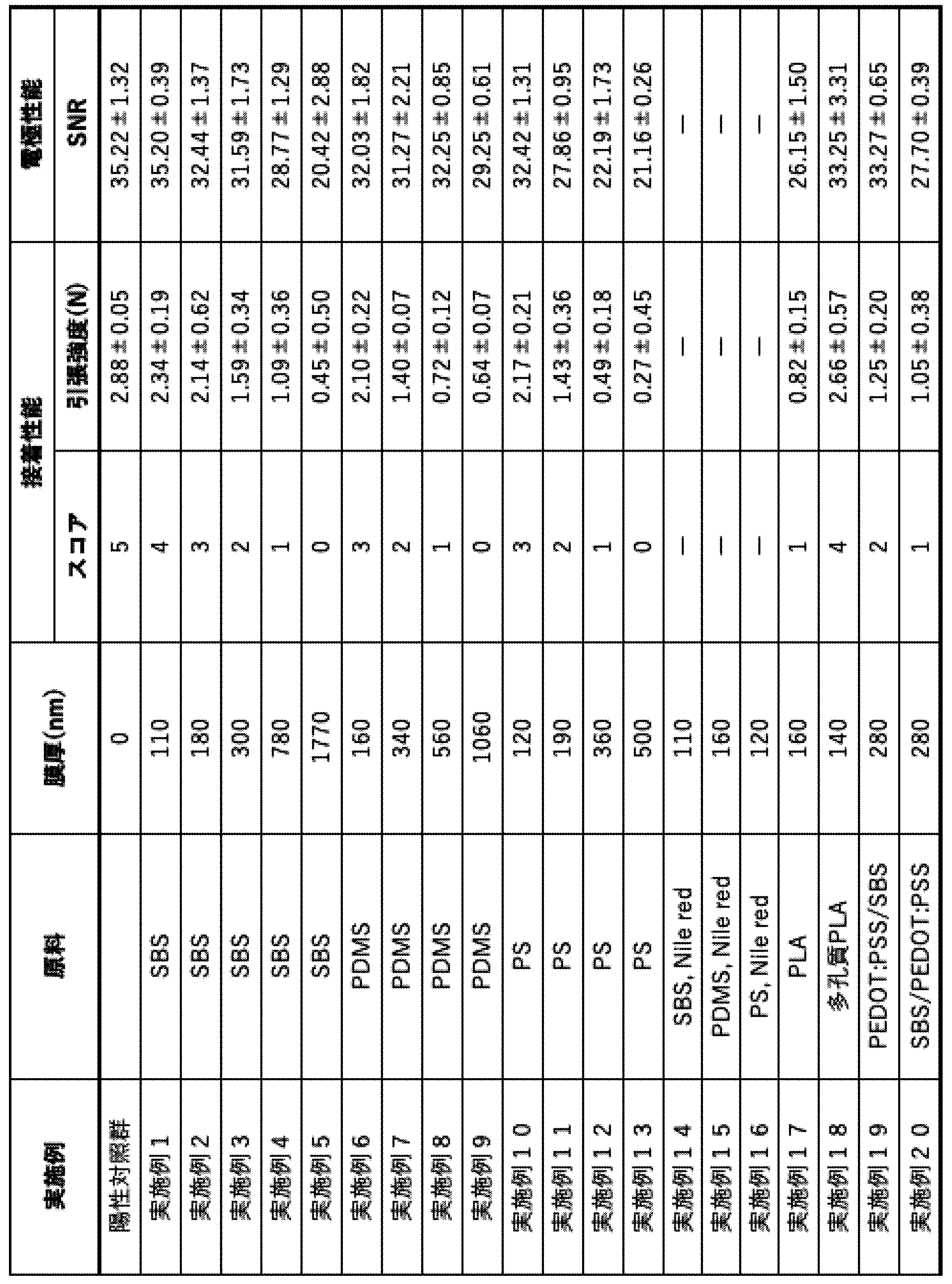
2.1.2.生体電極への貼付確認
明視野観察では高分子薄膜の貼付された面は観察困難であった。これは、50~2000nmの膜厚範囲である高分子薄膜が高い透明性を有し、生体電極に密に接しているためと考察される。一方で、蛍光顕微鏡下で観察すると、高分子薄膜が貼付されている面の境界がはっきりと視認することができた。また、いずれの高分子薄膜においても、しっかり貼付されている様子が観察された(図5)。
明視野観察では高分子薄膜の貼付された面は観察困難であった。これは、50~2000nmの膜厚範囲である高分子薄膜が高い透明性を有し、生体電極に密に接しているためと考察される。一方で、蛍光顕微鏡下で観察すると、高分子薄膜が貼付されている面の境界がはっきりと視認することができた。また、いずれの高分子薄膜においても、しっかり貼付されている様子が観察された(図5)。
まず、各実施例における接着性スコアを評価したところ、いずれの高分子薄膜においても、膜厚が減少するごとに接着性スコアが増大した(表5.図6)。特に、500nm未満となれば、いずれの実施例でも十分に接着性を有することが示された。
また、引張試験機を用いて接着力を定量的に評価したところ、接着スコアの結果と同様に、膜厚の減少とともに、接着力が増大し、接着性スコアと接着力とに正の相関関係があることが示された(表5、図7、図8、図9)。定性評価においてはスコア0の群においても、ある程度の接着力を保持可能であり、全く接着しないという結果ではなかった。また、接着性スコアの結果と同様に、500nm未満では十分な接着力を示し、特に200nm未満となると、元の生体電極の接着力と比べて80%程度の接着力を有していた。また、生体電極が異なると接着力の絶対値が異なるが、陽性対照群の接着力も異なっていることから、生体電極の固有性能の差である。
2.3.生体電極としての評価
低接着性生体電極の電極特性を評価した(表5)。各sEMG信号図を図10~図20にそれらの代表例を示した。
低接着性生体電極の電極特性を評価した(表5)。各sEMG信号図を図10~図20にそれらの代表例を示した。
高分子薄膜の膜厚が減少すると、SNR値は上昇し、より容易に筋電信号を取得することが可能であることが示された。特に、いずれの実施例においても、200nm未満の膜厚では陽性対照群と比べても10%程度の違いしかなく、電極としての特性を維持できることが判明した(図10~図20)。
また、多孔質PLA製の高分子薄膜(実施例18)を用いた低接着性生体電極は、生体電極の粘着ゲル層の接着性は低下するものの、多孔質PLA製の高分子薄膜と皮膚との接触性が向上するため、より良好に電極としての特性が維持されることが示された(図18)。
また、PEDOT:PSSとSBSの2層膜を高分子薄膜として使用した(実施例19,20)低接着性生体電極は、他の材料の高分子薄膜を用いた低接着性生体電極と比較して、より良好に電極としての特性が維持されることが示された(図19、図20)。
3.皮膚炎症試験
3.1.実験方法
低接着性生体デバイスの皮膚炎症に対する抑制効果をISO 10993-10:2010「医療機器の生物学的評価-第10部:炎症及び皮膚感作性の試験」に従って評価した。実施例の各高分子膜原料において膜厚が一番薄いもので作製した低接着性生体デバイスをヒト(N=3)の上腕内側部へ貼付し、2時間留置後、取り外した。取り外した直後、取り外してから1時間後及び2時間後に炎症の徴候を観察した。その後、皮膚炎症を表6の格付けに従って0から3の4段階で格付けすると同時に、各実験群における、取り外した直後、取り外してから1時間後及び2時間後の炎症の兆候の発生率を評価した。
3.1.実験方法
低接着性生体デバイスの皮膚炎症に対する抑制効果をISO 10993-10:2010「医療機器の生物学的評価-第10部:炎症及び皮膚感作性の試験」に従って評価した。実施例の各高分子膜原料において膜厚が一番薄いもので作製した低接着性生体デバイスをヒト(N=3)の上腕内側部へ貼付し、2時間留置後、取り外した。取り外した直後、取り外してから1時間後及び2時間後に炎症の徴候を観察した。その後、皮膚炎症を表6の格付けに従って0から3の4段階で格付けすると同時に、各実験群における、取り外した直後、取り外してから1時間後及び2時間後の炎症の兆候の発生率を評価した。
同時に、同一のヒトに対して、陽性対照群として、高分子薄膜を貼付しない既存の生体電極(日本光電製、ビトロード(登録商標)F150M)そのものを用いて、上腕部内側に貼付した後、取り外して、貼付部位の炎症症状の程度を観察した。
試験に使用した各実験群は以下のとおりである。
・陽性対照群:市販の生体電極(日本光電製、ビトロード(登録商標)F150M)
・SBS:実施例1の高分子薄膜を使用した低接着性生体デバイスをc
・PDMS:実施例6の高分子薄膜を使用した低接着性生体デバイス
・PS:実施例10の高分子薄膜を使用した低接着性生体デバイス
・PEDOT:PSS/SBS:実施例19の高分子薄膜を使用した低接着性生体デバイス
・PLA:実施例17の高分子薄膜を使用した低接着性生体デバイス
・多孔質PLA:実施例18の高分子薄膜を使用した低接着性生体デバイス
・陽性対照群:市販の生体電極(日本光電製、ビトロード(登録商標)F150M)
・SBS:実施例1の高分子薄膜を使用した低接着性生体デバイスをc
・PDMS:実施例6の高分子薄膜を使用した低接着性生体デバイス
・PS:実施例10の高分子薄膜を使用した低接着性生体デバイス
・PEDOT:PSS/SBS:実施例19の高分子薄膜を使用した低接着性生体デバイス
・PLA:実施例17の高分子薄膜を使用した低接着性生体デバイス
・多孔質PLA:実施例18の高分子薄膜を使用した低接着性生体デバイス
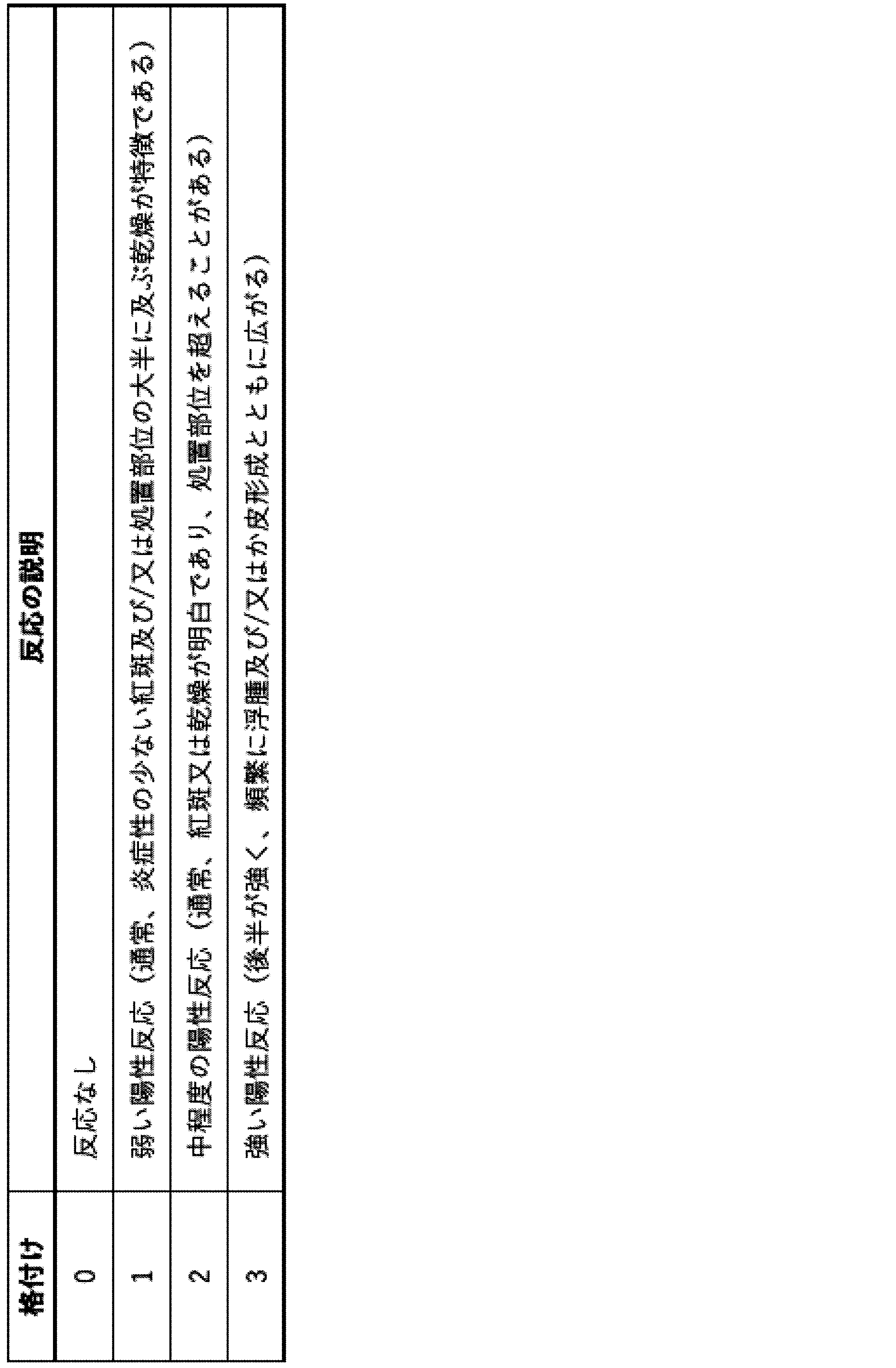
3.2.実験結果
低接着性生体デバイス群又は陽性対照群である市販の生体電極を2時間貼付して取り外した場合の、貼付前、貼付中、取り外した直後の様子を表す写真を、それぞれ図21A、図21B、図21Cに示した。
低接着性生体デバイス群又は陽性対照群である市販の生体電極を2時間貼付して取り外した場合の、貼付前、貼付中、取り外した直後の様子を表す写真を、それぞれ図21A、図21B、図21Cに示した。
陽性対照群では、生体電極を貼付後取り外した直後に100%の確率で皮膚炎症の中程度の陽性反応を示し、取り外し1時間後に約67%の発生率を示した(図22)。一方、低接着性生体デバイスを貼付した実験群は、いずれも「取り外し直後」の皮膚炎症の発生率が約67%以下であり、陽性対照群での発生率よりも小さい値となった。特に、PDMS群では、「取り外した直後」、「1時間後」及び「2時間後」のいずれにおいても、皮膚炎症の発生所見を認めなかった(図22)。
本結果より、本発明の低接着性デバイスが皮膚炎症等の有害事象の惹起を抑制し、有用であることを示すものである。
本発明の生体デバイスは、生体電極、グルコースセンサー、pHセンサー、イオンセンサー、ガスセンサー、体温計、加速度センサー及びひずみセンサー等として、皮膚等の臓器に接着して疾病の診断及び/又は治療に使用される生体デバイスとして利用できる。これらの生体デバイスは、脳波計、筋電計、心電計、電気刺激装置をはじめとした各種デバイスに使用できる。
1:生体電極
2:皮膚に貼付した高分子薄膜
11:高分子薄膜
12:粘着層
13:基材
14:電極
20:低接着性生体電極
30:皮膚
2:皮膚に貼付した高分子薄膜
11:高分子薄膜
12:粘着層
13:基材
14:電極
20:低接着性生体電極
30:皮膚
Claims (8)
- 接着する生体部位に対する接着性が低減された低接着性の生体デバイスであって、該生体デバイスは、電極部と、電極部の電極面に接着された粘着ゲル層と、該粘着ゲル層の表面に積層された高分子薄膜とを有し、生体との間で電気信号の授受能力を保持しつつ、前記粘着ゲル層の接着力よりも低減された生体への接着性を有する生体デバイス。
- 前記高分子薄膜が、複数層で形成されていることを特徴とする、請求項1に記載の
生体デバイス。 - 前記高分子薄膜の膜厚が50~2000nmであることを特徴とする、請求項1又は2に記載の生体デバイス。
- 前記粘着ゲル層の生体への接着力に対して、前記生体デバイスの生体への接着力の割合が、10~90%であることを特徴とする、請求項1~3のいずれか1項に記載の生体デバイス。
- 前記生体デバイスが、生体電極、グルコースセンサー、pHセンサー、イオンセンサー、ガスセンサー、体温計、加速度センサー又はひずみセンサーから選択されることを特徴とする請求項1~4のいずれか1項に記載の生体デバイス。
- 前記粘着ゲル層によって惹起される皮膚障害を予防又は軽減するための請求項1~5のいずれか1項に記載の生体デバイス。
- 請求項1~6に記載の生体デバイスの粘着ゲル層の表面に積層された高分子薄膜であって、電気信号の授受を保持しつつ、生体デバイスの粘着ゲルの接着性を低減するための高分子薄膜。
- 請求項1~6に記載の生体デバイスにおいて、高分子薄膜を積層することによる、電気信号の授受を保持しつつ生体デバイスの粘着ゲルの生体に対する接着性を低減させる方法。
Priority Applications (1)
| Application Number | Priority Date | Filing Date | Title |
|---|---|---|---|
| JP2022535292A JP7820820B2 (ja) | 2020-07-08 | 2021-07-02 | 低接着性生体デバイス |
Applications Claiming Priority (2)
| Application Number | Priority Date | Filing Date | Title |
|---|---|---|---|
| JP2020117766 | 2020-07-08 | ||
| JP2020-117766 | 2020-07-08 |
Publications (1)
| Publication Number | Publication Date |
|---|---|
| WO2022009792A1 true WO2022009792A1 (ja) | 2022-01-13 |
Family
ID=79552599
Family Applications (1)
| Application Number | Title | Priority Date | Filing Date |
|---|---|---|---|
| PCT/JP2021/025114 Ceased WO2022009792A1 (ja) | 2020-07-08 | 2021-07-02 | 低接着性生体デバイス |
Country Status (2)
| Country | Link |
|---|---|
| JP (1) | JP7820820B2 (ja) |
| WO (1) | WO2022009792A1 (ja) |
Cited By (1)
| Publication number | Priority date | Publication date | Assignee | Title |
|---|---|---|---|---|
| CN115282496A (zh) * | 2022-06-30 | 2022-11-04 | 深圳市恒天伟焱科技股份有限公司 | 光电针灸治疗装置 |
Citations (3)
| Publication number | Priority date | Publication date | Assignee | Title |
|---|---|---|---|---|
| JP2001057967A (ja) * | 2000-01-01 | 2001-03-06 | Advance Co Ltd | 生体用電極の製造方法 |
| JP2015531005A (ja) * | 2012-07-12 | 2015-10-29 | プレジデント アンド フェローズ オブ ハーバード カレッジ | 易滑性自己潤滑性ポリマー表面 |
| JP2020019842A (ja) * | 2018-07-30 | 2020-02-06 | 積水化成品工業株式会社 | ハイドロゲル |
Family Cites Families (2)
| Publication number | Priority date | Publication date | Assignee | Title |
|---|---|---|---|---|
| WO2002081024A1 (en) | 2001-04-04 | 2002-10-17 | Alza Corporation | Transdermal electrotransport delivery device including an antimicrobial compatible reservoir composition |
| US8238995B2 (en) | 2006-12-08 | 2012-08-07 | General Electric Company | Self-adhering electrodes and methods of making the same |
-
2021
- 2021-07-02 JP JP2022535292A patent/JP7820820B2/ja active Active
- 2021-07-02 WO PCT/JP2021/025114 patent/WO2022009792A1/ja not_active Ceased
Patent Citations (3)
| Publication number | Priority date | Publication date | Assignee | Title |
|---|---|---|---|---|
| JP2001057967A (ja) * | 2000-01-01 | 2001-03-06 | Advance Co Ltd | 生体用電極の製造方法 |
| JP2015531005A (ja) * | 2012-07-12 | 2015-10-29 | プレジデント アンド フェローズ オブ ハーバード カレッジ | 易滑性自己潤滑性ポリマー表面 |
| JP2020019842A (ja) * | 2018-07-30 | 2020-02-06 | 積水化成品工業株式会社 | ハイドロゲル |
Cited By (1)
| Publication number | Priority date | Publication date | Assignee | Title |
|---|---|---|---|---|
| CN115282496A (zh) * | 2022-06-30 | 2022-11-04 | 深圳市恒天伟焱科技股份有限公司 | 光电针灸治疗装置 |
Also Published As
| Publication number | Publication date |
|---|---|
| JPWO2022009792A1 (ja) | 2022-01-13 |
| JP7820820B2 (ja) | 2026-02-26 |
Similar Documents
| Publication | Publication Date | Title |
|---|---|---|
| Zhang et al. | Skin‐friendly electronics for acquiring human physiological signatures | |
| Lim et al. | Tissue-like skin-device interface for wearable bioelectronics by using ultrasoft, mass-permeable, and low-impedance hydrogels | |
| Zhang et al. | On-skin ultrathin and stretchable multifunctional sensor for smart healthcare wearables | |
| Zhang et al. | Fully organic compliant dry electrodes self-adhesive to skin for long-term motion-robust epidermal biopotential monitoring | |
| Hwang et al. | Multifunctional smart skin adhesive patches for advanced health care | |
| Baek et al. | Flexible polymeric dry electrodes for the long-term monitoring of ECG | |
| Li et al. | Robust, self‐adhesive, and low‐contact impedance polyvinyl alcohol/polyacrylamide dual‐network hydrogel semidry electrode for biopotential signal acquisition | |
| Hua et al. | Hydrogel-based bioelectronics and their applications in health monitoring | |
| Zhang et al. | Stretchable and durable HD-sEMG electrodes for accurate recognition of swallowing activities on complex epidermal surfaces | |
| Tan et al. | Advanced interfacial design for electronic skins with customizable functionalities and wearability | |
| Miyamoto et al. | Highly Precise, Continuous, Long‐Term Monitoring of Skin Electrical Resistance by Nanomesh Electrodes | |
| Wang et al. | A thermally responsive phase-change hydrogel for skin-mountable multifunctional sensors | |
| Zhuo et al. | Reusable free-standing hydrogel electronic tattoo sensors with superior performance | |
| Liu et al. | Functional adhesive hydrogels for biological interfaces | |
| Lan et al. | Highly skin-compliant polymeric electrodes with synergistically boosted conductivity toward wearable health monitoring | |
| Hou et al. | Highly stretchable self-adhesive PEDOT: PSS dry electrodes for biopotential monitoring | |
| Kim et al. | Transparent and Skin‐Attachable Silver Nanowire Electrodes Embedded on Dissolvable Polyurethane for Highly Conformable Wearable Electronics | |
| JP7820820B2 (ja) | 低接着性生体デバイス | |
| CN114360809A (zh) | 一种超薄可拉伸薄膜电极的制备方法 | |
| Xue et al. | A patterned mechanical–electrical coupled sensing patch for multimodal muscle function evaluation | |
| Jin et al. | Smart materials for wearable healthcare devices | |
| Jung et al. | Carbon nanofiber-based wearable patches for bio-potential monitoring | |
| Taniguchi et al. | Evaluation of Stability and Cytotoxicity of Self-Doped PEDOT Nanosheets in a Quasi-Biological Environment for Bioelectrodes | |
| He et al. | Mussel-inspired sticky self-healing conductive hydrogels composites for physiological electrical sensing | |
| CN113447544A (zh) | 一种可降解瞬态no传感器及其制备方法 |
Legal Events
| Date | Code | Title | Description |
|---|---|---|---|
| 121 | Ep: the epo has been informed by wipo that ep was designated in this application |
Ref document number: 21835928 Country of ref document: EP Kind code of ref document: A1 |
|
| ENP | Entry into the national phase |
Ref document number: 2022535292 Country of ref document: JP Kind code of ref document: A |
|
| NENP | Non-entry into the national phase |
Ref country code: DE |
|
| 122 | Ep: pct application non-entry in european phase |
Ref document number: 21835928 Country of ref document: EP Kind code of ref document: A1 |