WO2022000623A1 - 传输线模组及电磁兼容处理方法 - Google Patents
传输线模组及电磁兼容处理方法 Download PDFInfo
- Publication number
- WO2022000623A1 WO2022000623A1 PCT/CN2020/103466 CN2020103466W WO2022000623A1 WO 2022000623 A1 WO2022000623 A1 WO 2022000623A1 CN 2020103466 W CN2020103466 W CN 2020103466W WO 2022000623 A1 WO2022000623 A1 WO 2022000623A1
- Authority
- WO
- WIPO (PCT)
- Prior art keywords
- circuit board
- connector
- transmission line
- radio frequency
- line module
- Prior art date
- Legal status (The legal status is an assumption and is not a legal conclusion. Google has not performed a legal analysis and makes no representation as to the accuracy of the status listed.)
- Ceased
Links
Classifications
-
- H—ELECTRICITY
- H01—ELECTRIC ELEMENTS
- H01R—ELECTRICALLY-CONDUCTIVE CONNECTIONS; STRUCTURAL ASSOCIATIONS OF A PLURALITY OF MUTUALLY-INSULATED ELECTRICAL CONNECTING ELEMENTS; COUPLING DEVICES; CURRENT COLLECTORS
- H01R13/00—Details of coupling devices of the kinds covered by groups H01R12/70 or H01R24/00 - H01R33/00
- H01R13/648—Protective earth or shield arrangements on coupling devices, e.g. anti-static shielding
- H01R13/658—High frequency shielding arrangements, e.g. against EMI [Electro-Magnetic Interference] or EMP [Electro-Magnetic Pulse]
- H01R13/6581—Shield structure
-
- H—ELECTRICITY
- H01—ELECTRIC ELEMENTS
- H01R—ELECTRICALLY-CONDUCTIVE CONNECTIONS; STRUCTURAL ASSOCIATIONS OF A PLURALITY OF MUTUALLY-INSULATED ELECTRICAL CONNECTING ELEMENTS; COUPLING DEVICES; CURRENT COLLECTORS
- H01R12/00—Structural associations of a plurality of mutually-insulated electrical connecting elements, specially adapted for printed circuits, e.g. printed circuit boards [PCB], flat or ribbon cables, or like generally planar structures, e.g. terminal strips, terminal blocks; Coupling devices specially adapted for printed circuits, flat or ribbon cables, or like generally planar structures; Terminals specially adapted for contact with, or insertion into, printed circuits, flat or ribbon cables, or like generally planar structures
- H01R12/70—Coupling devices
- H01R12/77—Coupling devices for flexible printed circuits, flat or ribbon cables or like structures
- H01R12/79—Coupling devices for flexible printed circuits, flat or ribbon cables or like structures connecting to rigid printed circuits or like structures
-
- H—ELECTRICITY
- H01—ELECTRIC ELEMENTS
- H01R—ELECTRICALLY-CONDUCTIVE CONNECTIONS; STRUCTURAL ASSOCIATIONS OF A PLURALITY OF MUTUALLY-INSULATED ELECTRICAL CONNECTING ELEMENTS; COUPLING DEVICES; CURRENT COLLECTORS
- H01R13/00—Details of coupling devices of the kinds covered by groups H01R12/70 or H01R24/00 - H01R33/00
- H01R13/648—Protective earth or shield arrangements on coupling devices, e.g. anti-static shielding
- H01R13/658—High frequency shielding arrangements, e.g. against EMI [Electro-Magnetic Interference] or EMP [Electro-Magnetic Pulse]
- H01R13/6591—Specific features or arrangements of connection of shield to conductive members
- H01R13/6594—Specific features or arrangements of connection of shield to conductive members the shield being mounted on a PCB and connected to conductive members
-
- H—ELECTRICITY
- H05—ELECTRIC TECHNIQUES NOT OTHERWISE PROVIDED FOR
- H05K—PRINTED CIRCUITS; CASINGS OR CONSTRUCTIONAL DETAILS OF ELECTRIC APPARATUS; MANUFACTURE OF ASSEMBLAGES OF ELECTRICAL COMPONENTS
- H05K1/00—Printed circuits
- H05K1/02—Details
- H05K1/0213—Electrical arrangements not otherwise provided for
- H05K1/0216—Reduction of cross-talk, noise or electromagnetic interference
- H05K1/0218—Reduction of cross-talk, noise or electromagnetic interference by printed shielding conductors, ground planes or power plane
-
- H—ELECTRICITY
- H05—ELECTRIC TECHNIQUES NOT OTHERWISE PROVIDED FOR
- H05K—PRINTED CIRCUITS; CASINGS OR CONSTRUCTIONAL DETAILS OF ELECTRIC APPARATUS; MANUFACTURE OF ASSEMBLAGES OF ELECTRICAL COMPONENTS
- H05K2201/00—Indexing scheme relating to printed circuits covered by H05K1/00
- H05K2201/10—Details of components or other objects attached to or integrated in a printed circuit board
- H05K2201/10007—Types of components
- H05K2201/10189—Non-printed connector
Definitions
- the present application relates to the technical field of electrical components, and in particular, to a transmission line module and an electromagnetic compatibility processing method.
- the transmission line is provided with transmission parts (such as FPC, PCB) and connectors for connecting the transmission parts.
- transmission parts such as FPC, PCB
- the shielding effects of existing connectors from different connector manufacturers are uneven, and it is difficult to achieve the consistency of shielding effects on the same product. It is difficult for the existing connectors and transmission parts to achieve the electromagnetic compatibility indicators of higher frequency and wider bandwidth, and it is difficult to solve the above electromagnetic compatibility problems by changing the design of the existing connectors and transmission parts.
- the purpose of this application is to provide a transmission line module and an electromagnetic compatibility processing method, so as to solve the technical problem that it is difficult for the existing connectors and transmission components to achieve the electromagnetic compatibility indicators of higher frequency and wider bandwidth.
- a transmission line module comprising a first circuit board, a second circuit board and a connector connecting the first circuit board and the second circuit board;
- the transmission line module further includes an electrical connector electrically connecting the ground layer of the first circuit board and the ground layer of the second circuit board.
- An electromagnetic compatibility processing method applied to a transmission line structure, the transmission line structure comprising a first circuit board, a second circuit board and a connector connecting the first circuit board and the second circuit board, the method has the following step:
- the ground layer of the first circuit board and the ground layer of the second circuit board are electrically connected through electrical connectors.
- the beneficial effect of the present application is that the ground layer of the first circuit board and the ground layer of the second circuit board are electrically connected through the electrical connector, without changing the existing connector, the design of the first circuit board and the second circuit board, and without changing the Under the factors such as the connection position and connection method between the existing connector and the first circuit board and the second circuit board, the electromagnetic compatibility performance of the transmission line structure using the connectors of different connector manufacturers can be significantly improved, so that the The selection space is larger and more flexible; and the design of electrical connectors is flexible and easy to process.
- FIG. 1 is a schematic diagram of the positional relationship of a first circuit board, a second circuit board, a connector, and an electrical connector in the transmission line module of Embodiment 1;
- Fig. 2 is A-A sectional view in Fig. 1;
- Fig. 3 is the schematic diagram that the electrical connector is arranged far from the radio frequency transmission port group
- FIG. 4 is a schematic diagram of the positional relationship of the first circuit board, the second circuit board, the connector and the electrical connector in the transmission line module of Embodiment 2;
- Fig. 5 is B-B in Fig. 4 sectional view
- FIG. 6 is a schematic diagram of the positional relationship of the first circuit board, the second circuit board, the connector and the electrical connector in the transmission line module of the third embodiment
- Fig. 7 is the side view of Fig. 6;
- FIG. 8 is a schematic diagram of the positional relationship of the first circuit board, the second circuit board, the connector, and the electrical connector in the transmission line module of Embodiment 4;
- FIG. 9 is a schematic diagram of the positional relationship of the first circuit board, the second circuit board, the connector and the electrical connector in the transmission line module of Embodiment 5;
- Figure 10 is a graph showing the comparison of isolation between links
- FIG. 11 is a schematic diagram of the connection of the corresponding link 1 and link 2 in FIG. 10 .
- the transmission line module provided in this embodiment is used to improve the electromagnetic compatibility performance of the transmission line structure. Please refer to FIG. 1 to FIG. 9 together.
- the transmission line module includes a first circuit board 10 , a second circuit board 20 , and a connector 30 connecting the first circuit board 10 and the second circuit board 20 to realize Signals are transmitted between the first circuit board 10 and the second circuit board 20 .
- the first circuit board 10 is a PCB or an FPC.
- the second circuit board 20 is a PCB or an FPC. That is, the first circuit board 10 and the second circuit board 20 may be both PCBs or both FPCs or one of PCBs and FPCs, respectively.
- the first circuit board 10 is an FPC
- the second circuit board 20 is a PCB
- both the first circuit board 10 and the second circuit board 20 include at least one ground layer.
- the first circuit board 10 and the second circuit board 20 are respectively provided with male or female headers of the connector 30 . That is, the first circuit board 10 is provided with a male header and the second circuit board 20 is provided with a female header, or the first circuit board 10 is provided with a female header and the second circuit board 20 is provided with a male header.
- the male and female headers are connected to form the connector 30 , so that signals can be transmitted between the first circuit board 10 and the second circuit board 20 .
- the connector 30 includes at least one group of radio frequency transmission port groups, and each radio frequency transmission port group includes a first radio frequency transmission port 11 that is electrically connected to the first circuit board 10 and a second radio frequency transmission port that is electrically connected to the second circuit board 20.
- the port 21 and the connector 30 realize signal transmission between the first circuit board 10 and the second circuit board 20 through the first radio frequency transmission port 11 and the second radio frequency transmission port 21 .
- the male/female connector is connected to the RF signal line of the first circuit board 10 by connecting the first RF transmission port 11
- the male/female connector is connected to the RF signal line of the second circuit board 20 by connecting the second RF transmission port 21 line connection.
- the type of the connector 30 may be any as long as it can realize signal transmission between the first circuit board 10 and the second circuit board 20 .
- a transmission line module further includes electrical connectors 100, 200, 300, 400, 500, and the electrical connectors 100, 200, 300, 400, 500 connect the ground layers of the first circuit board 10 It is electrically connected to the ground layer of the second circuit board 20 .
- the ground layer of the first circuit board 10 and the ground layer of the second circuit board 20 are electrically connected through the electrical connectors 100 , 200 , 300 , 400 and 500 , without changing the existing connector 30 , the first circuit board 10 and the second circuit
- the design of the board 20 and the factors such as the connection position and connection method between the existing connector 30 and the first circuit board 10 and the second circuit board 20 can be significantly improved.
- the electromagnetic compatibility performance of the transmission line structure makes the selection space of the connector 30 larger and more flexible. In the case of electrical connection, the defect of uneven shielding effect of different connectors 30 can be compensated.
- the electrical connectors 100 , 200 , 300 , 400 , and 500 are located in the circumferential direction of the connector 30 with a gap therebetween.
- Connection terminals are formed on the electrical connectors 100 , 200 , 300 , 400 and 500 .
- the electrical connectors 100 , 200 , 300 , 400 and 500 are electrically connected to the ground layer of the first circuit board 10 and the ground layer of the second circuit board 20 through the connection terminals, so as to realize the ground layer of the first circuit board 10 and the ground layer of the second circuit board 20 .
- Electrical connection between ground layers In this embodiment, the connection terminals can be connected to the ground layer of the first circuit board 10 and the ground layer of the second circuit board 20 by welding or plugging.
- the electrical connectors 100 , 200 , 300 , 400 , 500 are made of conductive materials or the electrical connectors 100 , 200 , 300 , 400 , 500 have the ground layers of the first circuit board 10 and the ground layers of the second circuit board 20 .
- the conductive part of the electrical connection, the conductive part is made of conductive material.
- the conductive materials can be conductive metal materials and their alloys, composite metal materials, conductive plastics, conductive rubber, conductive fiber fabrics, conductive coatings, conductive adhesives, transparent conductive films, electronic conductive polymer materials and ion conductive polymer materials.
- the outer side of the conductive part can be wrapped with an insulating layer or a shielding layer to isolate the conductive part from the outside world.
- the electrical connectors 100, 200, 300, 400, 500 are disposed close to the radio frequency transmission port group.
- the connector 30 has a circumferential side wall in the circumferential direction, and the circumferential side wall has a first side wall section 31 closest to the radio frequency transmission port group and a second side wall section 32 next to the radio frequency transmission port group.
- Electrical connectors 100 , 200 , 300 , 400 , 500 are oppositely disposed on the outer sides of the side wall section 31 and/or the second side wall section 32 .
- the electrical connectors 100, 200, 300, 400, 500 are oppositely arranged on the outer side of the first side wall section 31, or the electrical connectors 100, 200, 300, 400, 500 are oppositely arranged on the outer side of the second side wall section 32, Alternatively, electrical connectors 100 , 200 , 300 , 400 , and 500 are oppositely disposed on the outer sides of the first side wall section 31 and the second side wall section 32 .
- the adjacent electrical connectors 100, 200, 300, 400, and 500 are connected as a whole.
- the adjacent electrical connectors 100, 200, 300, 400, 500 may be close to the two electrical connectors 100, 200, 300, 400, 500 of the same radio frequency transmission port group, and the two electrical connectors 100, 200, 300, 400 , 500 are respectively located on the outside of the first side wall section 31 and the second side wall section 32; the adjacent electrical connectors 100, 200, 300, 400, 500 may also be two electrical connectors close to different radio frequency transmission port groups respectively.
- Connectors 100, 200, 300, 400, 500 It can be understood that in other embodiments, the adjacent electrical connectors 100 , 200 , 300 , 400 , and 500 may also be provided independently without being connected to each other.
- Embodiment 1 The following is Embodiment 1:
- the first circuit board 10 includes a first body 12 and a first end 13 connected to the connector 30 .
- the second circuit board 20 includes a second body 22 and a second end 23 connected with the connector 30 .
- the first end 13 is provided with a male/female connector to connect with the female/male connector on the second end 23 to form a connector 30 .
- the first end 13 and the second end 23 are parallel to each other and are connected by a connector 30 .
- the connector 30 includes two radio frequency transmission port groups.
- the first radio frequency transmission port 11 and the second radio frequency transmission port 21 are disposed opposite to each other.
- the circumferential side wall of the connector 30 is a rectangular cylindrical surface.
- Both radio frequency transmission port groups are close to the side wall section of the same connector 30 , that is, the side wall section is the first side wall section 31 .
- the number of electrical connectors 100 is two and corresponds to two radio frequency transmission port groups one-to-one, and the two electrical connectors 100 are located between the first end 13 and the second end 23 and spaced from the connector 30 .
- the two electrical connectors 100 are integrally connected.
- the first side wall section 31 is disposed opposite to the first body 12 , and the electrical connector 100 is located between the first body 12 and the first side wall section 31 .
- the number of the electrical connectors 100 is one, two or more.
- the shape of the electrical connector 100 may be arbitrary. In this embodiment, the number of the electrical connector 100 is one.
- the electrical connector 100 has a plate shape and is parallel to the first side 31 . The left and right ends of the electrical connector 100 protrude outward from the plane where the corresponding second side wall section 32 is located. The upper and lower ends of the electrical connector 100 are respectively electrically connected to the ground layer of the first circuit board 10 and the ground layer of the second circuit board 20 .
- this embodiment also provides a comparative example, as shown in FIG. FIG. 3 differs from FIG. 1 only in the position of the electrical connector 100 .
- the electrical connector 100 in FIG. 3 is disposed away from the radio frequency transmission port group, which can be used as an arrangement of the electrical connector 100, but compared with the electrical connector 100 in FIG. 1 and FIG.
- the setup shown in Figure 3 is not optimal.
- a transmission line module which is different from the transmission line module in the first embodiment in that the electrical connector 200 is disposed outside the second side wall section 32 .
- the circumferential side wall of the connector 30 is a rectangular cylindrical surface.
- Connector 30 includes two sets of radio frequency transmission ports. Both radio frequency transmission port groups are close to the side wall section of the same connector 30 , that is, the side wall section is the first side wall section 31 .
- Each radio frequency transmission port group corresponds to a side wall segment next to it, that is, the side wall segment is the second side wall segment 32 . Therefore, in this embodiment, the number of the electrical connectors 200 is two, and the two electrical connectors 200 are provided separately and are not connected to each other.
- the electrical connector 200 is also in the shape of a plate.
- the two electrical connectors 200 are disposed in a one-to-one correspondence with the two second side wall sections 32 . Further, the electrical connector 200 is parallel to the second side wall segment 32 . One end of the electrical connector 200 located at the first side wall segment 31 protrudes outward from the plane where the first side wall segment 31 is located.
- a transmission line module which is different from the transmission line module in the first embodiment in that: the outer sides of the first side wall section 31 and the second side wall section 32 are both provided with electrical connections 300 pieces.
- the circumferential side wall of the connector 30 is a rectangular cylindrical surface.
- Connector 30 includes two sets of radio frequency transmission ports. Both radio frequency transmission port groups are close to the side wall section of the same connector 30 , that is, the side wall section is the first side wall section 31 .
- Each radio frequency transmission port group corresponds to a side wall segment next to it, that is, the side wall segment is the second side wall segment 32 .
- the number of the electrical connectors 300 is four, which are adjacent to the electrical connectors 300 of the same RF transmission port group and are connected as a whole, located in the same first sidewall section 31 and corresponding to different RF frequencies respectively.
- the two electrical connectors 300 of the transmission port group are adjacent to each other and connected as a whole, and the four electrical connectors 300 form a U-shaped groove.
- a transmission line module differs from the transmission line module in Embodiment 3 in that the electrical connector 400 is cylindrical, and the adjacent electrical connectors 400 are arranged separately and are not connected to each other.
- a transmission line module differs from the transmission line module in the fourth embodiment in that the electrical connector 500 is in the shape of a regular quadrangular prism.
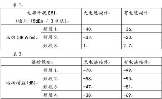
- Tables 1 and 2 are the electromagnetic interference performance test data of the transmission line module 1 with and without the electrical connector in Embodiment 1, and Table 2 is with and without Embodiment 1.
- Table 1 is the electromagnetic interference performance test data of the transmission line module 1 with and without the electrical connector in Embodiment 1
- Table 2 is with and without Embodiment 1.
- FIG. 10 is a graph showing the comparison of the isolation between the transmission line module 1 and the standard antenna 3 .
- the curves 1 and 2 are the isolation curves between the first radio frequency transmission port 11 of the transmission line module 1 and the standard antenna 3
- the curves 3 and 4 are the isolation curves between the second radio frequency transmission port 21 of the transmission line module 1 and the standard antenna 3 .
- the transmission line module 1 is not provided with electrical connectors
- the transmission line module 1 is provided with electrical connectors.
- the test scheme is shown in FIG.
- the electrical connector is beneficial to improve the electromagnetic compatibility performance of the transmission line module 1 .
- the transmission line structure includes a first circuit board, a second circuit board, and a connector connecting the first circuit board and the second circuit board, so as to realize the signal transmission between the first circuit board and the second circuit board. transfer between boards.
- the first circuit board is a PCB or FPC.
- the second circuit board is a PCB or FPC. That is, the first circuit board and the second circuit board can be both PCBs or both FPCs or one of PCBs and FPCs respectively.
- the first circuit board is an FPC
- the second circuit board is a PCB, both of which contain at least one ground layer.
- the first circuit board and the second circuit board are respectively provided with a male header and a female header, and the connector is formed by connecting the male header and the female header. That is, the first circuit board is provided with a male header and the second circuit board is provided with a female header, or the first circuit board is provided with a female header and the second circuit board is provided with a male header.
- the male header is connected with the female header to form a connector, so that signals can be transmitted between the first circuit board and the second circuit board.
- the connector includes at least one group of radio frequency transmission port groups, each radio frequency transmission port group includes a first radio frequency transmission port electrically connected with the first circuit board and a second radio frequency transmission port electrically connected with the second circuit board, the connector Signal transmission between the first circuit board and the second circuit board is achieved through the first radio frequency transmission port and the second radio frequency transmission port.
- the male/female connector is connected to the first circuit board by connecting to the first radio frequency transmission port
- the male/female connector is connected to the second circuit board by connecting to the second radio frequency transmission port.
- the connector type may be any as long as the signal can be transmitted between the first circuit board and the second circuit board.
- the method has the following steps:
- the ground layer of the first circuit board and the ground layer of the second circuit board are electrically connected through electrical connectors.
- the ground layer of the first circuit board and the ground layer of the second circuit board are electrically connected through electrical connectors, without changing the existing connector, the design of the first circuit board and the second circuit board, and without changing the existing connector and the first circuit board.
- the electromagnetic compatibility performance of the transmission line structure using connectors from different connector manufacturers can be significantly improved, so that the selection space of connectors is larger and more flexible. That is, when the electrical connector electrically connects the ground layer of the first circuit board and the ground layer of the second circuit board, the defect of uneven shielding effect of different connectors can be compensated.
- the electrical connector is located in the circumferential direction of the connector and has a gap with the connector.
- Connection terminals are formed on the electrical connector.
- the electrical connector is electrically connected to the ground layer of the first circuit board and the ground layer of the second circuit board through the connecting terminal, so as to realize the electrical connection between the ground layer of the first circuit board and the ground layer of the second circuit board.
- the connection terminals can be connected to the ground layer of the first circuit board and the ground layer of the second circuit board by welding or plugging.
- the electrical connector is made of conductive material or the electrical connector has a conductive portion for electrically connecting the ground layer of the first circuit board and the ground layer of the second circuit board, and the conductive portion is made of conductive material.
- the conductive materials can be conductive metal materials and their alloys, composite metal materials, conductive plastics, conductive rubber, conductive fiber fabrics, conductive coatings, conductive adhesives, transparent conductive films, electronic conductive polymer materials and ion conductive polymer materials.
- the outer side of the conductive part can be wrapped with an insulating layer or a shielding layer to isolate the conductive part from the outside world.
- the electrical connectors are arranged close to the radio frequency transmission port group.
- the circumferential direction of the connector has a circumferential side wall
- the circumferential side wall has a first side wall segment closest to the radio frequency transmission port group and a second side wall segment next to the radio frequency transmission port group, and the first side wall segment And/or the outer side of the second side wall section is oppositely provided with a connector. That is, the outer side of the first side wall segment is provided with the connector oppositely, or the outer side of the second side wall segment is provided with the connector oppositely, or the outer side of the first side wall segment and the second side wall segment are provided with the connector oppositely.
- the method also includes the following steps:
- the electromagnetic compatibility performance of the transmission line structure can be adjusted by changing one or more of the material, shape, number, position of the electrical connector and the size of the gap between the electrical connector and the connector in the circumferential direction.
Landscapes
- Physics & Mathematics (AREA)
- Electromagnetism (AREA)
- Engineering & Computer Science (AREA)
- Microelectronics & Electronic Packaging (AREA)
- Details Of Connecting Devices For Male And Female Coupling (AREA)
- Shielding Devices Or Components To Electric Or Magnetic Fields (AREA)
- Coupling Device And Connection With Printed Circuit (AREA)
- Structure Of Printed Boards (AREA)
Abstract
一种传输线模组(1)及电磁兼容处理方法。传输线模组(1)包括第一电路板(10)、第二电路板(20)以及连接第一电路板(10)和第二电路板(20)的连接器(30);传输线模组(1)还包括电连接件(100、200、300、400、500),电连接件(100、200、300、400、500)将第一电路板(10)的地层和第二电路板(20)的地层电连接。通过电连接件(100、200、300、400、500)将第一电路板(10)的地层和第二电路板(20)的地层电连接,在不改变现有连接器(30)、第一电路板(10)和第二电路板(20)的设计以及不改变现有连接器(30)与第一电路板(10)、第二电路板(20)之间的连接位置、连接方式等因素下,能够明显提升采用不同连接器厂家的连接器的传输线结构的电磁兼容性能,以使连接器的选择空间更大更灵活;并且电连接件设计灵活,加工简易。
Description
本申请涉及电气元件技术领域,具体涉及一种传输线模组及电磁兼容处理方法。
现终端设备随着技术的发展,传输线连接需要承载更高频率、更高速率的传输,而使用频段和带宽的增加,以及终端设备集成度的增加,随之带来了更多的电磁兼容问题(如电磁干扰EMI、电磁泄露、散射影响到其它传输链路)。
传输线设置有传输部件(如FPC、PCB)和用于连接传输部件的连接器。现有不同连接器厂家的连接器屏蔽效果参差不齐,很难在同一款产品上实现屏蔽效果的一致性。现有连接器及传输部件很难达到更高频率、更宽带宽的电磁兼容各项指标,而通过更改现有连接器及传输部件的设计来解决上述电磁兼容问题很困难。
因此,有必要提供一种传输线模组及电磁兼容处理方法。
本申请的目的在于提供一种传输线模组及电磁兼容处理方法,以解决现有连接器及传输部件很难达到更高频率、更宽带宽的电磁兼容各项指标的技术问题。
为了解决上述技术问题,本申请采用的技术方案一为:
一种传输线模组,所述传输线模组包括第一电路板、第二电路板以及连接所述第一电路板和所述第二电路板的连接器;
所述传输线模块还包括电连接件,所述电连接件将所述第一电路板的地层和所述第二电路板的地层电连接。
为了解决上述技术问题,本申请采用的技术方案二为:
一种电磁兼容处理方法,应用于传输线结构,所述传输线结构包括第一电路板、第二电路板和连接所述第一电路板和所述第二电路板的连接器,所述方法具有如下步骤:
将所述第一电路板的地层和所述第二电路板的地层通过电连接件电连接。
本申请的有益效果在于:通过电连接件将第一电路板的地层和第二电路板的地层电连接,在不改变现有连接器、第一电路板和第二电路板的设计以及不改变现有连接器与第一电路板、第二电路板之间的连接位置、连接方式等因素下,能够明显提升采用不同连接器厂家的连接器的传输线结构的电磁兼容性能,以使连接器的选择空间更大更灵活;并且电连接件设计灵活,加工简易。
图1为实施方式一的传输线模组中第一电路板、第二电路板、连接器和电连接件的位置关系示意图;
图2为图1中A-A向剖视图;
图3为电连接件远离射频传输端口组设置的示意图;
图4为实施方式二的传输线模组中第一电路板、第二电路板、连接器和电连接件的位置关系示意图;
图5为图4中B-B向剖视图;
图6为实施方式三的传输线模组中第一电路板、第二电路板、连接器和电连接件的位置关系示意图;
图7为图6的侧视图;
图8为实施方式四的传输线模组中第一电路板、第二电路板、连接器和电连接件的位置关系示意图;
图9为实施方式五的传输线模组中第一电路板、第二电路板、连接器和电连接件的位置关系示意图;
图10为链路间的隔离度对比曲线图;
图11为图10中对应的链路一和链路二的连接简图。
下面结合附图和实施方式对本申请作进一步说明。
本实施方式提供的传输线模组用于提升传输线结构的电磁兼容性能。请一并结合图1至图9,本实施方式中传输线模组包括第一电路板10、第二电路板20,以及连接第一电路板10和第二电路板20的连接器30,以实现信号在第一电路板10和第二电路板20之间传输。第一电路板10为PCB或FPC。第二电路板20为PCB或FPC。即第一电路板10和第二电路板20可以均为PCB或均为FPC或分别为PCB和FPC中的一种。本实施例中,第一电路板10为FPC,第二电路板20为PCB,第一电路板10和第二电路板20均含有至少一层地层。第一电路板10和第二电路板20分别设置有连接器30的公头或母头。即第一电路板10上设置有公头且第二电路板20上设置有母头,或第一电路板10上设置有母头且第二电路板20上设置有公头。公头与母头连接形成连接器30,以实现信号能够在第一电路板10和第二电路板20之间传输。进一步地,连接器30包括至少一组射频传输端口组,各射频传输端口组包括与第一电路板10电连接的第一射频传输端口11和与第二电路板20电连接的第二射频传输端口21,连接器30通过第一射频传输端口11和第二射频传输端口21实现第一电路板10与第二电路板20之间的信号传输。具体地,公头/母头通过连接第一射频传输端口11与第一电路板10的射频信号线连接,公头/母头通过连接第二射频传输端口21与第二电路板20的射频信号线连接。连接器30类型可以是任意的,只要能够实现信号在第一电路板10和第二电路板20之间传输即可。
请一并结合图1和图14,一种传输线模组还包括电连接件100、200、300、400、500,电连接件100、200、300、400、500将第一电路板10的地层和第二电路板20的地层电连接。通过电连接件100、200、300、400、500将第一电路板10的地层和第二电路板20的地层电连接,在不改变现有连接器30、第一电路板10和第二电路板20的设计以及不改变现有连接器30与第一电路板10、第二电路板20之间的连接位置、连接方式等因素下,能够明显提升采用不同连接器30厂家的连接器30的传输线结构的电磁兼容性能,以使连接器30的选择空间更大更灵活,即在电连接件100、200、300、400、500将第一电路板10的地层和第二电路板20的地层电连接的情况下,可以弥补不同连接器30屏蔽效果参差不齐的缺陷。
具体地,电连接件100、200、300、400、500位于连接器30的周向且与连接器30之间具有间隙。电连接件100、200、300、400、500上形成有连接端子。电连接件100、200、300、400、500通过连接端子与第一电路板10的地层和第二电路板20的地层电连接,以实现第一电路板10的地层和第二电路板20的地层之间电连接。本实施方式中,连接端子与第一电路板10的地层和第二电路板20的地层之间可通过焊接或插接的方式连接。进一步地,电连接件100、200、300、400、500由导电材料制成或电连接件100、200、300、400、500具有将第一电路板10的地层和第二电路板20的地层电连接的导电部,导电部由导电材料制成。导电材料可以为导电金属材料及其合金、复合金属材料、导电塑料、导电橡胶、导电纤维织物、导电涂料、导电胶粘剂、透明导电薄膜、电子导电高分子材料和离子导电高分子材料。导电部的外侧可包裹绝缘层或屏蔽层,以使导电部与外界隔开。
进一步地,电连接件100、200、300、400、500靠近射频传输端口组设置。具体地,连接器30的周向具有周向侧壁,周向侧壁具有最接近射频传输端口组的第一侧壁段31和次接近射频传输端口组的第二侧壁段32,第一侧壁段31和/或第二侧壁段32的外侧相对设置有电连接件100、200、300、400、500。即第一侧壁段31的外侧相对设置有电连接件100、200、300、400、500,或第二侧壁段32的外侧相对设置有电连接件100、200、300、400、500,或第一侧壁段31和第二侧壁段32的外侧均相对设置有电连接件100、200、300、400、500。
进一步地,相邻电连接件100、200、300、400、500连为一体。该相邻电连接件100、200、300、400、500可以靠近同一射频传输端口组的两个电连接件100、200、300、400、500,两个电连接件100、200、300、400、500分别位于第一侧壁段31和第二侧壁段32的外侧;该相邻电连接件100、200、300、400、500也可以为分别靠近不同的射频传输端口组的两个电连接件100、200、300、400、500。可以理解为在其他实施例中,相邻电连接件100、200、300、400、500也可以单独设置不互相连接。
下面通过具体实施方式对本申请做进一步说明。
以下为实施方式一:
请一并结合图1和图2,本实施方式中,第一电路板10包括第一本体12和与连接器30连接的第一端13。第二电路板20包括第二本体22和与连接器30连接的第二端23。第一端13上设置有公头/母头,以与第二端23上的母头/公头连接形成连接器30。第一端13和第二端23互相平行相对且通过连接器30连接。本实施方式中,连接器30包括两个射频传输端口组。第一射频传输端口11和第二射频传输端口21相对设置。连接器30的周向侧壁呈长方形柱面。两个射频传输端口组均靠近同一个连接器30的侧壁段,即该侧壁段为第一侧壁段31。具体地,电连接件100的数量为两个且一一对应于两个射频传输端口组,两个电连接件100位于第一端13和第二端23之间且与连接器30间隔。两个电连接件100连为一体。第一侧壁段31与第一本体12相对设置,电连接件100位于第一本体12和第一侧壁段31之间。
进一步地,电连接件100的数量为一个、两个或两个以上。电连接件100的形状可以是任意的。本实施例中,电连接件100的数量为一个。电连接件100呈板状且与第一侧31平行。电连接件100左右两端外凸于所对应的第二侧壁段32所在平面。电连接件100上下两端分别与第一电路板10的地层和第二电路板20的地层电连接。
为了对比说明电连接件100靠近射频传输端口组设置,本实施例还提供了一个对比例,如图3所示,为电连接件100远离射频传输端口组设置的示意图。图3与图1相比仅在电连接件100位置上有区别。图3中电连接件100为远离射频传输端口组设置,其可以作为一种电连接件100的设置方式,但与图1和图2中电连接件100靠近远离射频传输端口组设置相比,图3所示的设置方式不是最佳方式。
以下为实施方式二:
请一并结合图4和图5,一种传输线模组,其与实施方式一中传输线模组的区别特征为:电连接件200设置在第二侧壁段32的外侧。具体地,连接器30的周向侧壁呈长方形柱面。连接器30包括两个射频传输端口组。两个射频传输端口组均靠近同一个连接器30的侧壁段,即该侧壁段为第一侧壁段31。每个射频传输端口组对应一个次接近其的侧壁段,即该侧壁段为第二侧壁段32。因此,本实施例中,电连接件200的数量为两个,两个电连接件200单独设置不互相连接。本实施方式中,电连接件200同样呈板状。两个电连接件200一一对应相对两个第二侧壁段32设置。进一步地,电连接件200与第二侧壁段32平行。电连接件200位于第一侧壁段31的一端外凸于第一侧壁段31所在平面。
以下为实施方式三:
请一并结合图6和图7,一种传输线模组,其与实施方式一中传输线模组的区别特征为:第一侧壁段31和第二侧壁段32的外侧均设置有电连接件300。具体地,连接器30的周向侧壁呈长方形柱面。连接器30包括两个射频传输端口组。两个射频传输端口组均靠近同一个连接器30的侧壁段,即该侧壁段为第一侧壁段31。每个射频传输端口组对应一个次接近其的侧壁段,即该侧壁段为第二侧壁段32。因此,本实施例中,电连接件300的数量为四个,相对同一个射频传输端口组的电连接件300相邻且连为一体,位于同一第一侧壁段31且分别对应不同的射频传输端口组的两个电连接件300相邻且连为一体,四个电连接件300构成U形槽状。
以下为实施方式四:
如图8所示,一种传输线模组,其与实施方式三中传输线模组的区别特征为:电连接件400呈圆柱状,相邻电连接件400单独设置不互相连接。
以下为实施方式五:
如图9所示,一种传输线模组,其与实施方式四中传输线模组的区别特征为:电连接件500呈正四棱柱状。
经过测试实验,以上具有电连接件的传输线模组具有更优的电磁兼容性能。其部分性能参数如表1、2所示,其中表1为有、无实施方式一中的电连接件的传输线模组1的电磁干扰性能测试数据,表2为有、无实施方式一中的电连接件的传输线模组1的辐射散射性能测试数据。
另外,图10为传输线模组1与以标准天线3间的隔离度对比曲线图。其中,曲线1、2为传输线模组1的第一射频传输端口11与标准天线间3的隔离度曲线,曲线3、4为传输线模组1的第二射频传输端口21与标准天线3间的隔离度曲线,曲线2、4所表示的测试中,传输线模组1未设置电连接件,曲线1、3所表示的测试中,传输线模组1设置有电连接件。测试方案如图11所示,其中矢量网络分析仪4至标准天线3形成链路一2,矢量网络分析仪4至传输线模组1形成链路二5。由图10可知,电连接件有利于改善传输线模组1的电磁兼容性能。
以下为实施方式六:
一种电磁兼容处理方法,应用于传输线结构,传输线结构包括第一电路板、第二电路板和连接第一电路板和第二电路板的连接器,以实现信号在第一电路板和第二电路板之间传输。第一电路板为PCB或FPC。第二电路板为PCB或FPC。即第一电路板和第二电路板可以均为PCB或均为FPC或分别为PCB和FPC中的一种。本实施例中,第一电路板为FPC,第二电路板为PCB均含有至少一层地层。第一电路板和第二电路板分别设置有公头和母头,连接器通过公头与母头连接形成。即第一电路板上设置有公头且第二电路板上设置有母头,或第一电路板上设置有母头且第二电路板上设置有公头。公头与母头连接形成连接器,以实现信号能够在第一电路板和第二电路板之间传输。进一步地,连接器包括至少一组射频传输端口组,各射频传输端口组包括与第一电路板电连接的第一射频传输端口和与第二电路板电连接的第二射频传输端口,连接器通过第一射频传输端口和第二射频传输端口实现第一电路板与第二电路板之间的信号传输。具体地,公头/母头通过连接第一射频传输端口与第一电路板连接,公头/母头通过连接第二射频传输端口与第二电路板连接。连接器类型可以是任意的,只要能够实现信号在第一电路板和第二电路板之间传输即可。
该方法具有如下步骤:
将第一电路板的地层和第二电路板的地层通过电连接件电连接。通过电连接件将第一电路板的地层和第二电路板的地层电连接,在不改变现有连接器、第一电路板和第二电路板的设计以及不改变现有连接器与第一电路板、第二电路板之间的连接位置、连接方式等因素下,能够明显提升采用不同连接器厂家的连接器的传输线结构的电磁兼容性能,以使连接器的选择空间更大更灵活,即在电连接件将第一电路板的地层和第二电路板的地层电连接的情况下,可以弥补不同连接器屏蔽效果参差不齐的缺陷。
具体地,电连接件位于连接器的周向且与连接器之间具有间隙。电连接件上形成有连接端子。电连接件通过连接端子与第一电路板的地层和第二电路板的地层电连接,以实现第一电路板的地层和第二电路板的地层之间电连接。本实施方式中,连接端子与第一电路板的地层和第二电路板的地层之间可通过焊接或插接的方式连接。
进一步地,电连接件由导电材料制成或电连接件具有将第一电路板的地层和第二电路板的地层电连接的导电部,导电部由导电材料制成。导电材料可以为导电金属材料及其合金、复合金属材料、导电塑料、导电橡胶、导电纤维织物、导电涂料、导电胶粘剂、透明导电薄膜、电子导电高分子材料和离子导电高分子材料。导电部的外侧可包裹绝缘层或屏蔽层,以使导电部与外界隔开。
进一步地,电连接件靠近射频传输端口组设置。具体地,连接器的周向具有周向侧壁,周向侧壁具有最接近射频传输端口组的第一侧壁段和次接近射频传输端口组的第二侧壁段,第一侧壁段和/或第二侧壁段的外侧相对设置有连接器。即第一侧壁段的外侧相对设置有连接器,或第二侧壁段的外侧相对设置有连接器,或第一侧壁段和第二侧壁段的外侧均相对设置有连接器。
该方法还包括以下步骤:
通过改变电连接件的材质、形状、个数、位置以及电连接件与连接器周向之间的间隙大小中的一种或多种,调整传输线结构的电磁兼容性能。
以上的仅是本申请的实施方式,在此应当指出,对于本领域的普通技术人员来说,在不脱离本申请创造构思的前提下,还可以做出改进,但这些均属于本申请的保护范围。
Claims (9)
- 一种传输线模组,所述传输线模组包括第一电路板、第二电路板以及连接所述第一电路板和所述第二电路板的连接器,其特征在于:所述传输线模块还包括电连接件,所述电连接件将所述第一电路板的地层和所述第二电路板的地层电连接。
- 根据权利要求1所述的传输线模组,其特征在于,所述电连接件位于所述连接器的周向且与所述连接器之间具有间隙。
- 根据权利要求2所述的传输线模组,其特征在于,所述连接器包括至少一组射频传输端口组,各射频传输端口组包括与所述第一电路板电连接的第一射频传输端口和与所述第二电路板电连接的第二射频传输端口,所述连接器通过所述第一射频传输端口和所述第二射频传输端口实现所述第一电路板与所述第二电路板之间的信号传输;所述电连接件靠近所述射频传输端口组设置。
- 根据权利要求3所述的传输线模组,其特征在于,所述连接器的周向具有周向侧壁,所述周向侧壁具有最接近所述射频传输端口组的第一侧壁段和次接近所述射频传输端口组的第二侧壁段,所述第一侧壁段和/或所述第二侧壁段的外侧相对设置有所述电连接件。
- 根据权利要求4所述的传输线模组,其特征在于,相邻所述电连接件连为一体。
- 根据权利要求1至5任一权利要求所述的传输线模组,其特征在于,所述电连接件由导电材料制成或所述电连接件具有将所述第一电路板的地层和所述第二电路板的地层电连接的导电部,所述导电部由导电材料制成。
- 根据权利要求6所述的传输线模组,其特征在于,所述第一电路板为PCB或FPC;所述第二电路板为PCB或FPC。
- 一种电磁兼容处理方法,应用于传输线结构,所述传输线结构包括第一电路板、第二电路板和连接所述第一电路板和所述第二电路板的连接器,其特征在于,所述方法具有如下步骤:将所述第一电路板的地层和所述第二电路板的地层通过电连接件电连接。
- 根据权利要求8所述的方法,其特征在于:所述方法还包括以下步骤:通过改变所述电连接件的材质、形状、个数、位置以及所述电连接件与所述连接器周向之间的间隙大小中的一种或多种,调整所述传输线结构的电磁兼容性能。
Applications Claiming Priority (2)
| Application Number | Priority Date | Filing Date | Title |
|---|---|---|---|
| CN202010615335.X | 2020-06-30 | ||
| CN202010615335.XA CN111711032A (zh) | 2020-06-30 | 2020-06-30 | 传输线模组及电磁兼容处理方法 |
Publications (1)
| Publication Number | Publication Date |
|---|---|
| WO2022000623A1 true WO2022000623A1 (zh) | 2022-01-06 |
Family
ID=72543941
Family Applications (1)
| Application Number | Title | Priority Date | Filing Date |
|---|---|---|---|
| PCT/CN2020/103466 Ceased WO2022000623A1 (zh) | 2020-06-30 | 2020-07-22 | 传输线模组及电磁兼容处理方法 |
Country Status (2)
| Country | Link |
|---|---|
| CN (1) | CN111711032A (zh) |
| WO (1) | WO2022000623A1 (zh) |
Citations (7)
| Publication number | Priority date | Publication date | Assignee | Title |
|---|---|---|---|---|
| CN101026922A (zh) * | 2006-02-22 | 2007-08-29 | 鸿富锦精密工业(深圳)有限公司 | 电路板组合 |
| CN101861088A (zh) * | 2009-04-07 | 2010-10-13 | 纬创资通股份有限公司 | 电磁噪声抑制装置及其相关电子装置 |
| CN102522625A (zh) * | 2011-11-22 | 2012-06-27 | 上海安费诺永亿通讯电子有限公司 | 一种金属壳手机终端的天线结构 |
| US20130120957A1 (en) * | 2011-11-15 | 2013-05-16 | Apple Inc. | Rf shielding for electronic components |
| CN103414019A (zh) * | 2013-07-24 | 2013-11-27 | 珠海德百祺科技有限公司 | 天线和具有该天线的移动终端 |
| CN109066134A (zh) * | 2018-07-26 | 2018-12-21 | 维沃移动通信有限公司 | 一种连接件、电路板组件及终端设备 |
| CN110838652A (zh) * | 2018-08-17 | 2020-02-25 | 连展科技(深圳)有限公司 | 电连接器组件 |
Family Cites Families (1)
| Publication number | Priority date | Publication date | Assignee | Title |
|---|---|---|---|---|
| US9653847B2 (en) * | 2013-01-11 | 2017-05-16 | Sentinel Connector System, Inc. | High speed communication jack |
-
2020
- 2020-06-30 CN CN202010615335.XA patent/CN111711032A/zh active Pending
- 2020-07-22 WO PCT/CN2020/103466 patent/WO2022000623A1/zh not_active Ceased
Patent Citations (7)
| Publication number | Priority date | Publication date | Assignee | Title |
|---|---|---|---|---|
| CN101026922A (zh) * | 2006-02-22 | 2007-08-29 | 鸿富锦精密工业(深圳)有限公司 | 电路板组合 |
| CN101861088A (zh) * | 2009-04-07 | 2010-10-13 | 纬创资通股份有限公司 | 电磁噪声抑制装置及其相关电子装置 |
| US20130120957A1 (en) * | 2011-11-15 | 2013-05-16 | Apple Inc. | Rf shielding for electronic components |
| CN102522625A (zh) * | 2011-11-22 | 2012-06-27 | 上海安费诺永亿通讯电子有限公司 | 一种金属壳手机终端的天线结构 |
| CN103414019A (zh) * | 2013-07-24 | 2013-11-27 | 珠海德百祺科技有限公司 | 天线和具有该天线的移动终端 |
| CN109066134A (zh) * | 2018-07-26 | 2018-12-21 | 维沃移动通信有限公司 | 一种连接件、电路板组件及终端设备 |
| CN110838652A (zh) * | 2018-08-17 | 2020-02-25 | 连展科技(深圳)有限公司 | 电连接器组件 |
Also Published As
| Publication number | Publication date |
|---|---|
| CN111711032A (zh) | 2020-09-25 |
Similar Documents
| Publication | Publication Date | Title |
|---|---|---|
| TWI847482B (zh) | 電纜線連接器 | |
| US7645941B2 (en) | Shielded flexible circuits and methods for manufacturing same | |
| US8080738B2 (en) | Printed circuit having ground vias between signal vias | |
| WO2013096880A1 (en) | Capacitive blind-mate module interconnection | |
| WO2023273757A1 (zh) | 印刷电路板和电子设备 | |
| WO2021259021A1 (zh) | 印刷电路板及具有该印刷电路板的电子设备 | |
| CN106374279B (zh) | 集成贴装射频接插连接器 | |
| US9123980B2 (en) | Flexible transmission device and communication device using the same | |
| US6608258B1 (en) | High data rate coaxial interconnect technology between printed wiring boards | |
| Aihara et al. | Minimizing differential crosstalk of vias for high-speed data transmission | |
| WO2022000623A1 (zh) | 传输线模组及电磁兼容处理方法 | |
| WO2024198726A1 (zh) | 一种电路板和设备 | |
| CN106953150B (zh) | 双通道微带环行隔离组件 | |
| CN218334572U (zh) | 一种多芯带屏蔽结构高低频混装集成式矩形电连接器 | |
| US12069798B1 (en) | Broadside coupled radio frequency interconnect | |
| CN115911996A (zh) | 一种高速柔板连接组件 | |
| CN108288979B (zh) | 一种高速信号测试系统 | |
| US7205477B1 (en) | Surface mounted components using strip line conductors for surface wiring | |
| US20230413434A1 (en) | Circuit board with lower dielectric constant and electrical connector having the same | |
| US20260086118A1 (en) | Direct Connectorization for High-Frequency Signals | |
| US20210045244A1 (en) | Multiple circuit boards with high-density compression interconnect | |
| WO2022049410A1 (en) | Printed circuit board to printed circuit board radio frequency interface | |
| CN222214438U (zh) | 微带合路器装置和基站天线 | |
| TWI892426B (zh) | 毫米波電路結構及毫米波模組量測裝置 | |
| CN112909466B (zh) | 一种转接板、转接网络和天线 |
Legal Events
| Date | Code | Title | Description |
|---|---|---|---|
| 121 | Ep: the epo has been informed by wipo that ep was designated in this application |
Ref document number: 20943224 Country of ref document: EP Kind code of ref document: A1 |
|
| NENP | Non-entry into the national phase |
Ref country code: DE |
|
| 122 | Ep: pct application non-entry in european phase |
Ref document number: 20943224 Country of ref document: EP Kind code of ref document: A1 |