WO2021245831A1 - Adコンバータ - Google Patents
Adコンバータ Download PDFInfo
- Publication number
- WO2021245831A1 WO2021245831A1 PCT/JP2020/021900 JP2020021900W WO2021245831A1 WO 2021245831 A1 WO2021245831 A1 WO 2021245831A1 JP 2020021900 W JP2020021900 W JP 2020021900W WO 2021245831 A1 WO2021245831 A1 WO 2021245831A1
- Authority
- WO
- WIPO (PCT)
- Prior art keywords
- switch
- voltage
- current source
- unit
- error
- Prior art date
- Legal status (The legal status is an assumption and is not a legal conclusion. Google has not performed a legal analysis and makes no representation as to the accuracy of the status listed.)
- Ceased
Links
Images


Classifications
-
- H—ELECTRICITY
- H03—ELECTRONIC CIRCUITRY
- H03M—CODING; DECODING; CODE CONVERSION IN GENERAL
- H03M1/00—Analogue/digital conversion; Digital/analogue conversion
- H03M1/12—Analogue/digital converters
-
- H—ELECTRICITY
- H03—ELECTRONIC CIRCUITRY
- H03M—CODING; DECODING; CODE CONVERSION IN GENERAL
- H03M1/00—Analogue/digital conversion; Digital/analogue conversion
- H03M1/12—Analogue/digital converters
- H03M1/34—Analogue value compared with reference values
Definitions
- the present invention relates to an AD converter.
- the AD converter consists of a DA converter unit that outputs a known voltage, a sample hold unit that holds the voltage value of the analog input, and a comparator.
- the output value of the DA converter unit is sequentially changed and the output of the comparator is a low output voltage.
- the digital value when the output value of the minimum DA converter unit that changes from to high output voltage is set is used as the conversion value of the AD converter (Non-Patent Document 1).
- the present invention has been made in view of this problem, and an object of the present invention is to provide an AD converter that prevents deterioration of linearity due to parasitic capacitance and reduces conversion error.
- the AD converter according to one aspect of the present invention is an AD converter that repeats an operation of integrating a unit voltage into the initial value with an input voltage as an initial value, and holds a current source for generating the unit voltage and the initial value.
- the gist is to provide an error suppression unit that suppresses the movement of the charge accumulated in the parasitic capacity of the above.
- FIG. 1 It is a block diagram which shows the functional structure example of the AD converter which concerns on 1st Embodiment of this invention. It is a figure which shows the circuit model of the integration part which considered the parasitic capacitance. It is a figure which shows typically the change example of the terminal voltage of the parasitic capacitance shown in FIG. It is a figure which shows the circuit model of the integration part and the error suppression part shown in FIG. It is a figure which shows typically the change example of the terminal voltage of the parasitic capacitance shown in FIG. It is a block diagram which shows the functional structure example of the AD converter which concerns on 2nd Embodiment of this invention. It is a figure which shows the circuit model of the integration part and the error suppression part shown in FIG.
- FIG. 1 shows a block diagram of the AD converter according to the first embodiment of the present invention.
- AD converter 100 shown in FIG. 1 converts an input voltage to a digital value based on the integrated number of times the accumulated voltage integrated by unit voltage as an initial value by holding the input voltage to the capacitance C 0 is equal to the threshold voltage ..
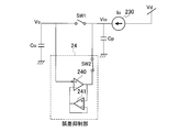
- the AD converter 100 is composed of a control unit and an integration conversion unit 20, and the integration conversion unit is composed of a third switch SW3, a threshold voltage unit 21, a comparator 22, an integration unit 23, and an error suppression unit 24. .. Further, the integration unit 23 is a current source 230, a first switch SW1, constituted by capacitance C 0.
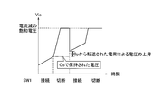
- FIG. 2 shows a circuit model of the integrating unit considering the parasitic capacitance of the current source and the switch.
- Cp represents parasitic capacitance.
- FIG. 3 shows the behavior of the voltage Vio of the output of the current source 230 in the circuit model of FIG. 2 with respect to the connection state of SW1.
- the switch SW1 When the switch SW1 is disconnected, the charge output from the current source 230 is stored only in the parasitic capacitance Cp.
- the parasitic capacitance Cp is an order of magnitude smaller than the capacitance Co, so that the voltage rises sharply due to the current from the current source 230.
- the voltage of the output of the current source 230 rises excessively, no current flows from the current source 230, and the voltage of the output of the current source 230, that is, the voltage of the parasitic capacitance Cp is saturated.
- the capacitance Co the electric charge is retained, so that the voltage is also retained.
- FIG. 4 shows a circuit model of the integrating unit 23 and the error suppressing unit 24 according to the first embodiment.
- the second switch SW2 is in the disconnected state when the first switch SW1 is in the connected state, and the second switch SW2 is in the connected state when the first switch SW1 is in the disconnected state.
- the output voltage Vio of the current source 230 is expressed by the following formula, assuming that the gain of the OP amplifier of the error suppression unit 24 is A1 and the offset voltage is Vof. Will be done.
- Vo and 0 represent the voltage of the capacitance Co. If the gain is large enough, Vio ⁇ Vo, 0.
- the voltage of the output of the current source 230 does not increase and becomes the same as Vo.
- FIG. 5 shows the behavior of Vio in this embodiment with respect to the connection state of SW1a. Even when the first switch SW1 is disconnected and the second switch SW2 is connected, Vio does not become the saturation voltage of the output of the current source 230 and is held in Vo.
- the present embodiment can provide an AD converter that prevents linear deterioration due to parasitic capacitance Cp and reduces conversion error.
- FIG. 6 shows a block diagram of the AD converter 200 according to the second embodiment of the present invention.
- the configuration of the error suppression unit 34 is different from that of the first embodiment.
- Regarding the relationship between the connection state of the first switch SW1, the second switch SW2, and the error correction switch SW4 when the first switch SW1 is in the connected state, the second switch SW2 is in the disconnected state, and a1 and c1 of the error correction switch SW4 are connected.
- the second switch SW2 is connected and the error correction switches SW4 a1 and b1 are connected.
- FIG. 7 shows the circuit model of this embodiment.
- a and Vof are the gain and offset voltage of the buffer amplifier (OP amplifier) 250, respectively.
- Vo, 0 represents the voltage of Co in this switch state.
- the charges Qs, 0 and Qp, 0 stored in the error suppression capacitance Cs and the parasitic capacitance Cp are expressed by the following equations.
- the electrode of the error suppression capacitance Cs connected to the output of the buffer amplifier 250 is the + pole.
- the transfer of electric charge when the first switch SW1 is connected, the second switch SW2 is disconnected, and the error correction switches SW4 a1 and c1 are connected will be considered.
- the voltage of the capacitance Co in this switch state is Vo, 1, the following equation holds because the charge conservation law holds before and after the change in the switch state.
- the second term on the right side represents the effect of the charge accumulated in the parasitic capacitance Cp on Vo, 1.
- the error suppression unit 25 of the AD converter 200 has an error suppression capacity Cs having a capacity value similar to that of the parasitic capacity Cp of the current source 230 and the first switch SW1 and a voltage held by the capacity Co.
- the buffer amplifier 250 that generates the duplicated integrated voltage and the first switch SW1 connect the error suppression capacitance Cs between the current source 230 and the common potential at the time of connection, and the first switch SW1 is charged to the error suppression capacitance Cs at the time of disconnection. It includes an error correction switch SW4 that reduces the error suppression voltage from the integrated voltage, and a second switch SW2 that reduces the error suppression voltage from the integrated voltage and connects the voltage to the output of the current source when the first switch SW1 disconnects. This makes it possible to provide an AD converter that prevents deterioration of linearity due to parasitic capacitance Cp and reduces conversion error.
- the present invention is not limited to the above embodiment, and can be modified within the scope of the gist thereof. It goes without saying that the present invention includes various embodiments not described here. Therefore, the technical scope of the present invention is defined only by the matters specifying the invention relating to the reasonable claims from the above description.
- Control unit 20 Integration conversion unit 21: Threshold voltage unit 22: Comparator 23: Integration unit 24: Error suppression unit 240: First operational amplifier 241: Second operational amplifier SW1: 1st switch SW2: 2nd switch SW3: 3rd switch SW4: Error correction switch
Landscapes
- Engineering & Computer Science (AREA)
- Theoretical Computer Science (AREA)
- Analogue/Digital Conversion (AREA)
Priority Applications (2)
| Application Number | Priority Date | Filing Date | Title |
|---|---|---|---|
| PCT/JP2020/021900 WO2021245831A1 (ja) | 2020-06-03 | 2020-06-03 | Adコンバータ |
| JP2022529214A JP7530007B2 (ja) | 2020-06-03 | 2020-06-03 | Adコンバータ |
Applications Claiming Priority (1)
| Application Number | Priority Date | Filing Date | Title |
|---|---|---|---|
| PCT/JP2020/021900 WO2021245831A1 (ja) | 2020-06-03 | 2020-06-03 | Adコンバータ |
Publications (1)
| Publication Number | Publication Date |
|---|---|
| WO2021245831A1 true WO2021245831A1 (ja) | 2021-12-09 |
Family
ID=78830707
Family Applications (1)
| Application Number | Title | Priority Date | Filing Date |
|---|---|---|---|
| PCT/JP2020/021900 Ceased WO2021245831A1 (ja) | 2020-06-03 | 2020-06-03 | Adコンバータ |
Country Status (2)
| Country | Link |
|---|---|
| JP (1) | JP7530007B2 (https=) |
| WO (1) | WO2021245831A1 (https=) |
Citations (2)
| Publication number | Priority date | Publication date | Assignee | Title |
|---|---|---|---|---|
| JP2003158446A (ja) * | 2001-11-20 | 2003-05-30 | Oki Electric Ind Co Ltd | チョッパ型コンパレータ |
| US20140085117A1 (en) * | 2012-09-21 | 2014-03-27 | Analog Devices, Inc. | Sampling circuit, a method of reducing distortion in a sampling circuit, and an analog to digital converter including such a sampling circuit |
Family Cites Families (3)
| Publication number | Priority date | Publication date | Assignee | Title |
|---|---|---|---|---|
| JP7079914B2 (ja) * | 2018-11-12 | 2022-06-03 | 日本電信電話株式会社 | 自己校正機能付きadコンバータ |
| JP7315868B2 (ja) | 2019-05-21 | 2023-07-27 | 日本電信電話株式会社 | 自己校正機能付きadコンバータ |
| JP7328579B2 (ja) | 2019-12-10 | 2023-08-17 | 日本電信電話株式会社 | Adコンバータ |
-
2020
- 2020-06-03 JP JP2022529214A patent/JP7530007B2/ja active Active
- 2020-06-03 WO PCT/JP2020/021900 patent/WO2021245831A1/ja not_active Ceased
Patent Citations (2)
| Publication number | Priority date | Publication date | Assignee | Title |
|---|---|---|---|---|
| JP2003158446A (ja) * | 2001-11-20 | 2003-05-30 | Oki Electric Ind Co Ltd | チョッパ型コンパレータ |
| US20140085117A1 (en) * | 2012-09-21 | 2014-03-27 | Analog Devices, Inc. | Sampling circuit, a method of reducing distortion in a sampling circuit, and an analog to digital converter including such a sampling circuit |
Also Published As
| Publication number | Publication date |
|---|---|
| JPWO2021245831A1 (https=) | 2021-12-09 |
| JP7530007B2 (ja) | 2024-08-07 |
Similar Documents
| Publication | Publication Date | Title |
|---|---|---|
| JP5062293B2 (ja) | サンプルホールド回路及びa/d変換装置 | |
| US9635298B2 (en) | Comparator circuit, imaging apparatus using the same, and method of controlling comparator circuit | |
| US8106806B2 (en) | AD converter | |
| US9407839B2 (en) | Solid-state imaging device | |
| US10224355B2 (en) | Comparator for low-banding noise and CMOS image sensor including the same | |
| US9787927B2 (en) | Solid-state imaging apparatus | |
| JPH06120827A (ja) | A/d変換器 | |
| US20210159866A1 (en) | Switched capacitor amplifier circuit, voltage amplification method, and infrared sensor device | |
| EP1408315A1 (en) | Photosensor | |
| WO2011104761A1 (ja) | パイプライン型a/dコンバータおよびa/d変換方法 | |
| US9413377B1 (en) | Switched capacitor circuit and compensation method thereof, and analog to digital converter | |
| US6407592B2 (en) | Sample-and-hold circuit | |
| WO2021245831A1 (ja) | Adコンバータ | |
| JP2009027282A (ja) | サンプルホールド回路およびパイプラインad変換器 | |
| JPS61126823A (ja) | アナログデイジタル変換器 | |
| JP7239863B2 (ja) | 自己校正機能付きadコンバータ | |
| JP7328579B2 (ja) | Adコンバータ | |
| US12126352B2 (en) | Semiconductor device and control method for the same | |
| US6906658B2 (en) | Reducing droop in a reference signal provided to ADCs | |
| US7342443B2 (en) | Operational amplifier | |
| JP6241989B2 (ja) | オフセットキャンセル回路及びこの回路を用いた信号検出回路 | |
| US20090231036A1 (en) | Amplifier circuit | |
| JPH0918290A (ja) | スイッチトキャパシタ回路 | |
| TWI677821B (zh) | 電壓減法器及其電壓相減的運算方法 | |
| KR101105461B1 (ko) | 연산 증폭기 및 이를 이용한 파이프 라인 아날로그 디지털 변환기 |
Legal Events
| Date | Code | Title | Description |
|---|---|---|---|
| 121 | Ep: the epo has been informed by wipo that ep was designated in this application |
Ref document number: 20939105 Country of ref document: EP Kind code of ref document: A1 |
|
| ENP | Entry into the national phase |
Ref document number: 2022529214 Country of ref document: JP Kind code of ref document: A |
|
| NENP | Non-entry into the national phase |
Ref country code: DE |
|
| 122 | Ep: pct application non-entry in european phase |
Ref document number: 20939105 Country of ref document: EP Kind code of ref document: A1 |