WO2021235485A1 - 電力変換装置および電力変換装置の製造方法 - Google Patents
電力変換装置および電力変換装置の製造方法 Download PDFInfo
- Publication number
- WO2021235485A1 WO2021235485A1 PCT/JP2021/018982 JP2021018982W WO2021235485A1 WO 2021235485 A1 WO2021235485 A1 WO 2021235485A1 JP 2021018982 W JP2021018982 W JP 2021018982W WO 2021235485 A1 WO2021235485 A1 WO 2021235485A1
- Authority
- WO
- WIPO (PCT)
- Prior art keywords
- cooling body
- main surface
- printed circuit
- circuit board
- substrate
- Prior art date
- Legal status (The legal status is an assumption and is not a legal conclusion. Google has not performed a legal analysis and makes no representation as to the accuracy of the status listed.)
- Ceased
Links
Images


Classifications
-
- H—ELECTRICITY
- H02—GENERATION; CONVERSION OR DISTRIBUTION OF ELECTRIC POWER
- H02M—APPARATUS FOR CONVERSION BETWEEN AC AND AC, BETWEEN AC AND DC, OR BETWEEN DC AND DC, AND FOR USE WITH MAINS OR SIMILAR POWER SUPPLY SYSTEMS; CONVERSION OF DC OR AC INPUT POWER INTO SURGE OUTPUT POWER; CONTROL OR REGULATION THEREOF
- H02M1/00—Details of apparatus for conversion
- H02M1/32—Means for protecting converters other than automatic disconnection
- H02M1/327—Means for protecting converters other than automatic disconnection against abnormal temperatures
-
- H—ELECTRICITY
- H02—GENERATION; CONVERSION OR DISTRIBUTION OF ELECTRIC POWER
- H02M—APPARATUS FOR CONVERSION BETWEEN AC AND AC, BETWEEN AC AND DC, OR BETWEEN DC AND DC, AND FOR USE WITH MAINS OR SIMILAR POWER SUPPLY SYSTEMS; CONVERSION OF DC OR AC INPUT POWER INTO SURGE OUTPUT POWER; CONTROL OR REGULATION THEREOF
- H02M3/00—Conversion of DC power input into DC power output
- H02M3/003—Constructional details, e.g. physical layout, assembly, wiring or busbar connections
-
- H—ELECTRICITY
- H02—GENERATION; CONVERSION OR DISTRIBUTION OF ELECTRIC POWER
- H02M—APPARATUS FOR CONVERSION BETWEEN AC AND AC, BETWEEN AC AND DC, OR BETWEEN DC AND DC, AND FOR USE WITH MAINS OR SIMILAR POWER SUPPLY SYSTEMS; CONVERSION OF DC OR AC INPUT POWER INTO SURGE OUTPUT POWER; CONTROL OR REGULATION THEREOF
- H02M3/00—Conversion of DC power input into DC power output
- H02M3/22—Conversion of DC power input into DC power output with intermediate conversion into AC
- H02M3/24—Conversion of DC power input into DC power output with intermediate conversion into AC by static converters
- H02M3/28—Conversion of DC power input into DC power output with intermediate conversion into AC by static converters using discharge tubes with control electrode or semiconductor devices with control electrode to produce the intermediate AC
- H02M3/285—Single converters with a plurality of output stages connected in parallel
-
- H—ELECTRICITY
- H02—GENERATION; CONVERSION OR DISTRIBUTION OF ELECTRIC POWER
- H02M—APPARATUS FOR CONVERSION BETWEEN AC AND AC, BETWEEN AC AND DC, OR BETWEEN DC AND DC, AND FOR USE WITH MAINS OR SIMILAR POWER SUPPLY SYSTEMS; CONVERSION OF DC OR AC INPUT POWER INTO SURGE OUTPUT POWER; CONTROL OR REGULATION THEREOF
- H02M3/00—Conversion of DC power input into DC power output
- H02M3/22—Conversion of DC power input into DC power output with intermediate conversion into AC
- H02M3/24—Conversion of DC power input into DC power output with intermediate conversion into AC by static converters
- H02M3/28—Conversion of DC power input into DC power output with intermediate conversion into AC by static converters using discharge tubes with control electrode or semiconductor devices with control electrode to produce the intermediate AC
- H02M3/325—Conversion of DC power input into DC power output with intermediate conversion into AC by static converters using discharge tubes with control electrode or semiconductor devices with control electrode to produce the intermediate AC using devices of a triode or a transistor type requiring continuous application of a control signal
- H02M3/335—Conversion of DC power input into DC power output with intermediate conversion into AC by static converters using discharge tubes with control electrode or semiconductor devices with control electrode to produce the intermediate AC using devices of a triode or a transistor type requiring continuous application of a control signal using semiconductor devices only
- H02M3/33569—Conversion of DC power input into DC power output with intermediate conversion into AC by static converters using discharge tubes with control electrode or semiconductor devices with control electrode to produce the intermediate AC using devices of a triode or a transistor type requiring continuous application of a control signal using semiconductor devices only having several active switching elements
- H02M3/33573—Full-bridge at primary side of an isolation transformer
-
- H—ELECTRICITY
- H05—ELECTRIC TECHNIQUES NOT OTHERWISE PROVIDED FOR
- H05K—PRINTED CIRCUITS; CASINGS OR CONSTRUCTIONAL DETAILS OF ELECTRIC APPARATUS; MANUFACTURE OF ASSEMBLAGES OF ELECTRICAL COMPONENTS
- H05K1/00—Printed circuits
- H05K1/18—Printed circuits structurally associated with non-printed electric components
- H05K1/181—Printed circuits structurally associated with non-printed electric components associated with surface mounted components
-
- H—ELECTRICITY
- H05—ELECTRIC TECHNIQUES NOT OTHERWISE PROVIDED FOR
- H05K—PRINTED CIRCUITS; CASINGS OR CONSTRUCTIONAL DETAILS OF ELECTRIC APPARATUS; MANUFACTURE OF ASSEMBLAGES OF ELECTRICAL COMPONENTS
- H05K3/00—Apparatus or processes for manufacturing printed circuits
- H05K3/0058—Laminating printed circuit boards onto other substrates, e.g. metallic substrates
- H05K3/0061—Laminating printed circuit boards onto other substrates, e.g. metallic substrates onto a metallic substrate, e.g. a heat sink
-
- H—ELECTRICITY
- H05—ELECTRIC TECHNIQUES NOT OTHERWISE PROVIDED FOR
- H05K—PRINTED CIRCUITS; CASINGS OR CONSTRUCTIONAL DETAILS OF ELECTRIC APPARATUS; MANUFACTURE OF ASSEMBLAGES OF ELECTRICAL COMPONENTS
- H05K7/00—Constructional details common to different types of electric apparatus
- H05K7/20—Modifications to facilitate cooling, ventilating, or heating
- H05K7/2089—Modifications to facilitate cooling, ventilating, or heating for power electronics, e.g. for inverters for controlling motor
- H05K7/209—Heat transfer by conduction from internal heat source to heat radiating structure
-
- H—ELECTRICITY
- H05—ELECTRIC TECHNIQUES NOT OTHERWISE PROVIDED FOR
- H05K—PRINTED CIRCUITS; CASINGS OR CONSTRUCTIONAL DETAILS OF ELECTRIC APPARATUS; MANUFACTURE OF ASSEMBLAGES OF ELECTRICAL COMPONENTS
- H05K1/00—Printed circuits
- H05K1/02—Details
- H05K1/14—Structural association of two or more printed circuits
- H05K1/148—Arrangements of two or more hingeably connected rigid printed circuit boards, i.e. connected by flexible means
-
- H—ELECTRICITY
- H05—ELECTRIC TECHNIQUES NOT OTHERWISE PROVIDED FOR
- H05K—PRINTED CIRCUITS; CASINGS OR CONSTRUCTIONAL DETAILS OF ELECTRIC APPARATUS; MANUFACTURE OF ASSEMBLAGES OF ELECTRICAL COMPONENTS
- H05K2201/00—Indexing scheme relating to printed circuits covered by H05K1/00
- H05K2201/04—Assemblies of printed circuits
- H05K2201/047—Box-like arrangements of PCBs
-
- H—ELECTRICITY
- H05—ELECTRIC TECHNIQUES NOT OTHERWISE PROVIDED FOR
- H05K—PRINTED CIRCUITS; CASINGS OR CONSTRUCTIONAL DETAILS OF ELECTRIC APPARATUS; MANUFACTURE OF ASSEMBLAGES OF ELECTRICAL COMPONENTS
- H05K3/00—Apparatus or processes for manufacturing printed circuits
- H05K3/36—Assembling printed circuits with other printed circuits
- H05K3/366—Assembling printed circuits with other printed circuits substantially perpendicularly to each other
Definitions
- the present disclosure relates to a power conversion device and a method for manufacturing the power conversion device.
- the power conversion device includes electronic parts such as switching elements, rectifying elements, and magnetic parts. These electronic components generate heat as the power converter operates. The heat generated by these electronic components is transferred to the cooling body through the heat dissipation path, and is dissipated from the cooling body. In this way, the temperature of these electronic components is suppressed below the permissible temperature of each electronic component.
- Patent Document 1 Japanese Patent No. 4231626 (Patent Document 1) describes an automobile motor drive device.
- the power conversion element which is a high heat generation component
- the bottom surface of the housing in which the power conversion element is arranged is integrated with the cooling body.
- the printed circuit board on which the control element is mounted is fixed to the plate-shaped substrate mounting portion formed inside the housing. The heat generated by the control element is transferred to the housing via the plate-shaped substrate mounting portion. Further, the printed circuit board is laminated on the power conversion element.
- a power conversion element which is a high heat generation component
- the power conversion device becomes large.
- the heat generated by the control element is transferred to the housing via the plate-shaped substrate stationary portion. Therefore, the heat dissipation path becomes long. As a result, heat dissipation is reduced.
- the electrical connection technique between the component and the printed circuit board is not described in detail. Therefore, for example, when two printed circuit boards are connected to each other by a screw and a terminal block for fixing the harness and the harness, the Joule heat generated in the screw and the terminal block raises the temperature of the power converter.
- the present disclosure has been made in view of the above problems, and an object thereof is to suppress an expansion of the bottom area of the power conversion device, improve heat dissipation, and increase the temperature of the power conversion device. It is an object of the present invention to provide a power conversion device that can be suppressed and a method for manufacturing the power conversion device.
- the power conversion device of the present disclosure includes an electronic component, a first board, a first cooling body, a second board, a second cooling body, and a first wiring member.
- Electronic components include first and second components.
- the first substrate has a first main surface on which the first component of an electronic component is mounted and a second main surface facing the first main surface.
- the first cooling body is thermally connected to the second main surface of the first substrate.
- the second substrate has a third main surface on which the second component of the electronic component is mounted and a fourth main surface facing the third main surface.
- the second cooling body is thermally connected to the fourth main surface of the second substrate.
- the first wiring member electrically connects the first board and the second board.
- the second cooling body extends from the second main surface of the first substrate toward the first main surface.
- the first wiring member is connected to the first main surface of the first substrate and the third main surface of the second substrate by either direct connection or soldering joint, respectively.
- the electronic components are mounted not only on the first board but also on the second board. Therefore, even when the number of electronic components that are high heat generating components increases, the expansion of the first cooling body can be suppressed by mounting the electronic components on the second substrate. Therefore, it is possible to suppress the expansion of the bottom area of the power conversion device. Further, by mounting the electronic component on the second substrate, it is possible to shorten the heat dissipation distance in which the heat generated by the electronic component mounted on the second substrate is transferred to the second cooling body. Therefore, the heat dissipation of the second substrate can be improved. Further, the first wiring member is connected to the first main surface of the first substrate and the third main surface of the second substrate by either direct connection or soldering joint, respectively.
- FIG. It is a circuit diagram of the power conversion apparatus which concerns on Embodiment 1.
- FIG. It is a perspective view schematically showing the structure of the power conversion apparatus which concerns on Embodiment 1.
- FIG. It is a perspective view schematically showing the structure of the 1st printed circuit board module of the power conversion apparatus which concerns on Embodiment 1.
- FIG. It is a perspective view schematically showing the structure of the 2nd printed circuit board module of the power conversion apparatus which concerns on Embodiment 1.
- FIG. It is a perspective view schematically showing the structure of the 3rd printed circuit board module of the power conversion apparatus which concerns on Embodiment 1.
- FIG. It is sectional drawing which shows typically the structure of the power conversion apparatus which concerns on Embodiment 1.
- FIG. 3 is a perspective view schematically showing a configuration of a power conversion device according to a modification 3 of the first embodiment.
- FIG. 3 is a perspective view schematically showing a configuration of a power conversion device according to a modification 4 of the first embodiment.
- FIG. 5 is a perspective view schematically showing a configuration of a power conversion device according to a modification 5 of the first embodiment.
- FIG. 5 is a perspective view schematically showing a configuration of a power conversion device according to a modification 6 of the first embodiment.
- It is a perspective view schematically showing the structure of the power conversion apparatus which concerns on Embodiment 2.
- FIG. It is a perspective view which shows typically the structure of the power conversion apparatus which concerns on the modification of Embodiment 2.
- It is a perspective view schematically showing the structure of the power conversion apparatus which concerns on Embodiment 3.
- FIG. It is a perspective view for demonstrating the electrical connection between the printed circuit board modules of the power conversion apparatus which concerns on Embodiment 3.
- FIG. It is a perspective view for demonstrating the electrical connection between the printed circuit board modules of the power conversion apparatus which concerns on the modification of Embodiment 3.
- FIG. It is sectional drawing which shows typically the structure of the power conversion apparatus which concerns on Embodiment 4.
- FIG. It is a perspective view for demonstrating the electrical connection between the printed circuit board modules of the power conversion apparatus which concerns on Embodiment 5.
- FIG. It is sectional drawing which shows typically the structure of the power conversion apparatus which concerns on Embodiment 6.
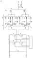
- FIG. 1 is an example of a circuit diagram of the power conversion device according to the first embodiment.
- the power conversion device shown in the circuit diagram of FIG. 1 is mounted on an electric vehicle, for example, and converts an input voltage of a lithium ion battery of DC100V to 300V into a voltage of DC12 to 15V and outputs the voltage to charge a lead storage battery. It is a DC-DC converter.
- the power conversion device shown in the circuit diagram of FIG. 1 includes an input capacitor 1, an inverter circuit unit 11 composed of four switching elements 2a, 2b, 2c and 2d, and a transformer unit 12 composed of transformers 3 and 4.
- the input is a rectifying circuit unit 13 composed of eight rectifying elements 5a, 5b, 5c, 5d, 5e, 5f, 5g, and 5h, a smoothing circuit unit 14 composed of reactors 6, 7, and a smoothing capacitor 8.
- a terminal 9, an output terminal 10, and a control circuit unit 15 are provided.
- each electronic component shown by a circuit symbol in FIG. 1 may have an arbitrary number of series configurations or parallel configurations.
- Each of the switching elements 2a, 2b, 2c, and 2d is a power semiconductor element such as a transistor, a MOSFET (Metal Oxide Semiconductor, Field Effect Transistor), and an IGBT (Insulated Gate Bipolar Transistor).
- the rectifying elements 5a, 5b, 5c, 5d, 5e, 5f, 5g, and 5h are power semiconductor elements such as diodes, MOSFETs, and thyristors.
- the power conversion device shown in the circuit diagram of FIG. 1 converts the DC voltage input from the input terminal 9 into an AC voltage by switching and controlling the inverter circuit unit 11 by the control circuit unit 15.
- the transformer unit 12 converts the AC voltage converted by the inverter circuit unit 11 into an arbitrary voltage according to the turns ratio of the transformers 3 and 4. Further, the transformers 3 and 4 electrically insulate between the input terminal 9 and the output terminal 10.
- the rectifier circuit unit 13 converts the AC voltage supplied from the transformers 3 and 4 into a DC voltage again.
- the smoothing circuit unit 14 smoothes the DC voltage converted by the rectifying circuit unit 13 to stabilize the output voltage.
- the wiring itself that electrically connects the high heat generation parts also generates a high heat generation amount. Therefore, when electrically connecting high heat-generating components with a circuit pattern formed on or inside the printed circuit board, it is necessary to dissipate the heat generated by the circuit pattern and keep the printed circuit board at an allowable temperature or lower.
- the permissible temperature of the printed circuit board is, for example, 100 ° C. or higher and 120 ° C. or lower.
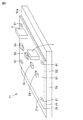
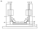
- FIG. 2 is a perspective view of the power conversion device 100 according to the first embodiment.
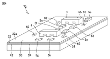
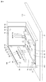
- FIG. 3 is a perspective view of the first printed circuit board module 71 included in the power conversion device 100.
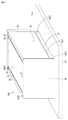
- FIG. 4 is a perspective view of the second printed circuit board module 72 included in the power conversion device 100.
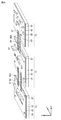
- FIG. 5 is a perspective view of the third printed circuit board module 73 included in the power conversion device 100. Note that the wiring member 86 and the joint portion 87, which will be described later, are not shown in FIGS. 2 to 5 for convenience of explanation.
- the power conversion device 100 includes an external cooling body 21, a first printed circuit board 31, a first insulating member 41, a first cooling body 51, and a first fixing member 61.
- the external cooling body 21 has a main surface 21a.
- the first printed circuit board (first board) 31 has a front surface (first main surface) S1 on which electronic components (first components) are mounted and a back surface (second main surface) S2 facing the first cooling body 51. have.
- the second main surface S2 faces the first main surface S1.
- the first insulating member 41 is arranged between the second main surface S2 of the first printed circuit board 31 and the first cooling body 51.
- the first cooling body 51 is thermally connected to the second main surface S2 of the first printed circuit board 31.
- the first cooling body 51 is thermally connected to the second main surface S2 of the first printed circuit board 31 via the first insulating member 41.
- the first cooling body 51 is thermally coupled to the external cooling body 21.
- the external cooling body 21 is thermally connected to the first cooling body 51.
- the first cooling body 51 is thermally connected to the second main surface S2 of the first printed circuit board 31.
- the first fixing member 61 is configured to fix the first printed circuit board 31 to the first cooling body 51.
- the second printed circuit board (second board) 32 has a front surface (third main surface) S3 on which electronic components (second components) are mounted and a back surface (fourth main surface) S4 facing the second cooling body 52. have.
- the fourth main surface S4 faces the third main surface S3.
- the second insulating member 42 is arranged between the fourth main surface S4 of the second printed circuit board 32 and the second cooling body 52.
- the second cooling body 52 is thermally connected to the fourth main surface S4 of the second printed circuit board 32.
- the second cooling body 52 is thermally connected to the fourth main surface S4 of the second printed circuit board 32 via the second insulating member 42.
- the second cooling body 52 is configured to extend vertically with the surface connected to the surface 51a of the first cooling body 51 facing the first printed circuit board 31 as the bottom surface.
- the second cooling body 52 extends from the second main surface S2 of the first printed circuit board 31 toward the first main surface S1.
- the second cooling body 52 is thermally connected to the first cooling body 51.
- the second fixing member 62 is configured to fix the second printed circuit board 32 to the second cooling body 52.
- the third printed circuit board (third board) 33 has a front surface (fifth main surface) S5 on which electronic components (third components) are mounted and a back surface (sixth main surface) S6 facing the third cooling body 53. have.
- the sixth main surface S6 faces the fifth main surface S5.
- the third insulating member 43 is arranged between the sixth main surface S6 of the third printed circuit board 33 and the third cooling body 53.
- the third cooling body 53 is thermally connected to the sixth main surface S6 of the third printed circuit board 33.
- the third cooling body 53 is thermally connected to the sixth main surface S6 of the third printed circuit board 33 via the third insulating member 43.
- the third cooling body 53 is configured to extend vertically with the surface connected to the surface 51a of the first cooling body 51 as the bottom surface.
- the third cooling body 53 extends from the second main surface S2 of the first printed circuit board 31 toward the first main surface S1.
- the third cooling body 53 is thermally connected to the first cooling body 51.
- the third fixing member 63 is configured to fix the third printed circuit board 33 to the third cooling body 53.
- Each of the second printed circuit board 32 and the third printed circuit board 33 extends in the direction from the second main surface S2 of the first printed circuit board 31 toward the first main surface S1.
- the second printed circuit board 32 and the third printed circuit board 33 are arranged so as to face each other.
- the first printed circuit board 31, the second printed circuit board, and the third printed circuit board 33 are configured inside the space composed of the cooling body.
- the second printed circuit board 32 and the third printed circuit board 33 are arranged so as to face each other, but they may be arranged so as to be adjacent to each other. At that time, the second printed circuit board 32 and the third printed circuit board 33 are thermally coupled.
- the vertical direction is a direction substantially perpendicular to the main surface 21a of the external cooling body 21.
- the first cooling body 51 constitutes the bottom surface of the support of the power conversion device 100.
- the second cooling body 52 and the third cooling body 53 form the side surface of the support of the power conversion device 100.
- the input power is connected to the first printed circuit board 31 from the upper opening of the second cooling body 52 or the third cooling body 53 by wiring such as a harness or a printed circuit board (not shown).
- the output power is output from the second printed circuit board 32 or the third printed circuit board 33.
- the second printed circuit board 32 or the third printed circuit board 33 for example, wiring of a harness or a printed circuit board for outputting output power is connected from an opening on the upper side of the housing (not shown).
- the control circuit unit 15 is arranged above the second cooling body 52 or the third cooling body 53 (not shown).
- the external cooling body 21 has a thermal conductivity of 1.0 W / (m ⁇ K) or more, preferably 10.0 W / (m ⁇ K) or more, and more preferably 100.0 W / (m ⁇ K) or more.
- the external cooling body 21 is formed of a metal material such as copper, iron, aluminum, an iron alloy, or an aluminum alloy, or a resin having a high thermal conductivity.
- the external cooling body 21 may be provided with a pipe for passing cooling water inside. Further, the external cooling body 21 may be provided with heat dissipation fins or the like in order to promote heat dissipation to the surrounding atmosphere.
- Each of the first printed circuit board 31, the second printed circuit board 32, and the third printed circuit board 33 may have a circuit pattern (not shown) formed on the surface or inside thereof.
- This circuit pattern has a thickness of 1 ⁇ m or more and 2000 ⁇ m or less.
- this circuit pattern is formed from a conductive material.
- This circuit pattern is formed from, for example, copper, nickel, gold, aluminum, silver, tin, etc. or alloys thereof.
- the materials constituting each of the first printed circuit board 31, the second printed circuit board 32, and the third printed circuit board 33 include, for example, glass fiber reinforced epoxy resin, phenol resin, polyphenylene sulfide (PPS), polyetheretherketone (PEEK), and the like. do it.
- each of the first printed circuit board 31, the second printed circuit board 32, and the third printed circuit board 33 may be made of a material generally having a low thermal conductivity. That is, each of the first printed circuit board 31, the second printed circuit board 32, and the third printed circuit board 33 may be a general-purpose printed circuit board. Further, each of the first printed circuit board 31, the second printed circuit board 32, and the third printed circuit board 33 may be made of ceramics such as aluminum oxide, aluminum nitride, and silicon carbide.
- Each of the first insulating member 41, the second insulating member 42, and the third insulating member 43 has electrical insulation. Further, each of the first insulating member 41, the second insulating member 42, and the third insulating member 43 may have elasticity. Further, each of the first insulating member 41, the second insulating member 42, and the third insulating member 43 may have a Young's modulus of 1 MPa or more and 100 MPa or less. Each of the first insulating member 41, the second insulating member 42, and the third insulating member 43 has a thermal conductivity of 0.1 W / (m ⁇ K) or more, preferably 1.0 W / (m ⁇ K) or more. ..
- Each of the first insulating member 41, the second insulating member 42 and the third insulating member 43 is made of, for example, a rubber material such as silicon or urethane, acrylonitrile butadiene styrene (ABS), polybutylene terephthalate (PBT), or polyphenylene sulfide (. It may be composed of a resin material such as PPS), a resin material such as phenol, a polymer material such as polyimide, a ceramic material such as alumina and aluminum nitride, and a phase change material containing silicon as a main raw material.
- a rubber material such as silicon or urethane, acrylonitrile butadiene styrene (ABS), polybutylene terephthalate (PBT), or polyphenylene sulfide (. It may be composed of a resin material such as PPS), a resin material such as phenol, a polymer material such as polyimide, a ceramic material such
- each of the first insulating member 41, the second insulating member 42, and the third insulating member 43 may be made of a material in which particles such as aluminum oxide, aluminum nitride, and boron nitride are mixed with a silicon resin.
- Each of the first cooling body 51, the second cooling body 52 and the third cooling body 53 is 1.0 W / (m ⁇ K) or more, preferably 10.0 W / (m ⁇ K) or more, more preferably 100. It has a thermal conductivity of 0 W / (m ⁇ K) or more.
- Each of the first cooling body 51, the second cooling body 52, and the third cooling body 53 is formed of a metal material such as copper, iron, aluminum, an iron alloy, or an aluminum alloy, or a resin having high thermal conductivity. ..
- the first cooling body 51, the second cooling body 52, and the third cooling body 53 are made of a plate-shaped aluminum alloy.
- each of the first cooling body 51, the second cooling body 52, and the third cooling body 53 may be electrically connected to another member so as to have the same potential as the ground. Further, each of the second cooling body 52 and the third cooling body 53 is connected to and fixed to the first cooling body 51 directly or via another member. Each of the second cooling body 52 and the third cooling body 53 is thermally connected to the first cooling body 51.
- a heat conductive grease, a heat conductive sheet, and a heat conductive adhesive are formed on the contact surface between the first cool body 51 and the second cool body 52 and the contact surface between the first cool body 51 and the third cool body 53.
- the heat conductive member (first heat conductive member) HC1 such as the above may be arranged.
- the heat conductive member (first heat conductive member) HC1 contains at least one of a heat conductive grease, a heat conductive sheet and a heat conductive adhesive.
- the first cooling body 51 is thermally connected to each of the second cooling body 52 and the third cooling body 53 via a heat conductive member (first heat conductive member) HC1.
- the first cooling body 51 may come into surface contact with the external cooling body 21.
- a heat conductive grease, a heat conductive sheet, a heat conductive adhesive, or the like is provided on the contact surface between the first cooling body 51 and the external cooling body 21.
- a heat conductive member may be arranged.
- the heat dissipation to the heat generated in the first printed circuit board module 71 is generated in the second printed circuit board module 72 and the third printed circuit board module 73. Higher than heat dissipation. Therefore, the electronic components arranged in the first printed circuit board module 71, the second printed circuit board module 72, and the third printed circuit board module 73 may be replaced, but the first printed circuit board module 71 generates particularly high heat generation electrons. It is preferable to arrange parts (high heat generation parts).
- each of the switching elements 2a, 2b, 2c, and 2d is a particularly heat-generating component
- each of the switching elements 2a, 2b, 2c, and 2d is attached to the first printed circuit board module 71. Deploy.
- the rectifying elements 5a, 5b, 5c, 5e, 5f, 5g, 5h or transformers 3 and 4 that generate less heat than the switching elements are arranged in the second printed circuit board module 72 and the third printed circuit board module 73.
- the first printed circuit board module 71 includes a first printed circuit board 31, a first insulating member 41, a first cooling body 51, a first fixing member 61, and an electronic component (first component). ) And.
- the electronic component (first component) is mounted on the first printed circuit board 31.
- the electronic component (first component) is each of the switching elements 2a, 2b, 2c, and 2d, which are particularly high heat generating components.
- the first insulating member 41 is provided between the first printed circuit board 31 and the first cooling body 51.
- the first insulating member 41 preferably comes into surface contact with the first printed circuit board 31 and the first cooling body 51.
- the first fixing member 61 fixes the first printed circuit board 31 to the first cooling body 51.
- the input capacitor 1 and the switching elements 2a, 2b, 2c, and 2d are mounted on the surface 31a of the first printed circuit board 31 opposite to the surface facing the first cooling body 51.
- An input terminal 9 (not shown) is mounted on the surface 31a.
- Other electronic components may be mounted on the surface 31a.
- other electronic components may be mounted on the surface of the first printed circuit board 31 facing the first cooling body 51.
- the surface of the first printed circuit board 31 facing the first cooling body 51 corresponds to the second main surface S2.
- the surface 31a of the first printed circuit board 31 opposite to the surface facing the first cooling body 51 corresponds to the first main surface S1.
- the second printed circuit board module 72 includes a second printed circuit board 32, a second insulating member 42, a second cooling body 52, a second fixing member 62, and an electronic component (second component). ) And.
- the electronic component (second component) is mounted on the second printed circuit board 32.
- the electronic components (second component) are transformers 3 and 4, which are particularly high heat generating components, and rectifying elements 5a, 5b, 5c, 5d, 5e, 5f, 5g, and 5h.
- the second insulating member 42 is provided between the fourth main surface S4 of the second printed circuit board 32 and the second cooling body 52.
- the second insulating member 42 preferably comes into surface contact with the second printed circuit board 32 and the second cooling body 52.
- the second fixing member 62 fixes the second printed circuit board 32 to the second cooling body 52.
- Rectifying elements 5a, 5b, 5c, 5d, 5e, 5f, 5g, 5h, and transformers 3 and 4 are mounted on the surface 32a of the second printed circuit board 32 opposite to the surface facing the second cooling body 52. Has been done. Other electronic components may be mounted on the surface 32a. Further, other electronic components may be mounted on the surface of the second printed circuit board 32 facing the second cooling body 52.
- the surface of the second printed circuit board 32 facing the second cooling body 52 corresponds to the fourth main surface S4.
- the surface 32a of the second printed circuit board 32 opposite to the surface facing the second cooling body 52 corresponds to the third main surface S3.
- the third printed circuit board module 73 includes a third printed circuit board 33, a third insulating member 43, a third cooling body 53, a third fixing member 63, and an electronic component (third component). ) And.
- the electronic component (third component) is mounted on the third printed circuit board 33.
- the electronic parts (third parts) are reactors 6 and 7, which are particularly high heat generating parts.
- the third insulating member 43 is provided between the third printed circuit board 33 and the third cooling body 53.
- the third insulating member 43 preferably comes into surface contact with the third printed circuit board 33 and the third cooling body 53.
- the third fixing member 63 fixes the third printed circuit board 33 to the third cooling body 53.
- the smoothing capacitor 8 and the reactors 6 and 7 are mounted on the surface 33a of the third printed circuit board 33 opposite to the surface facing the third cooling body 53. Further, an output terminal 10 (not shown) is mounted on the surface 33a. Further, other electronic components may be mounted on the surface 33a. Further, other electronic components may be mounted on the surface of the third printed circuit board 33 facing the third cooling body 53.
- the surface of the third printed circuit board 33 facing the third cooling body 53 corresponds to the sixth main surface S6.
- the surface 33a of the third printed circuit board 33 opposite to the surface facing the third cooling body 53 corresponds to the fifth main surface S5.
- the control circuit unit 15 shown in FIG. 1 may be mounted on any of the first printed circuit board 31, the second printed circuit board 32, and the third printed circuit board 33. Further, the control circuit unit 15 may be divided and mounted on at least two or more printed circuit boards among the first printed circuit board 31, the second printed circuit board 32, and the third printed circuit board 33.
- the power conversion device 100 includes an external cooling body 21, a first printed circuit board module 71, a second printed circuit board module 72, and a third printed circuit board module 73. ing.
- the wiring member 86 electrically connects between the first printed circuit board module 71 and the second printed circuit board module 72, and between the first printed circuit board module 71 and the third printed circuit board module 73.
- the wiring member 86 includes a first wiring member 86a and a second wiring member 86b.
- the first wiring member 86a electrically connects the first printed circuit board 31 of the first printed circuit board module 71 and the second printed circuit board 32 of the second printed circuit board module 72.
- the second wiring member 86b electrically connects the first printed circuit board 31 of the first printed circuit board module 71 and the third printed circuit board 33 of the third printed circuit board module 73.
- the first wiring member 86a is connected to the first main surface S1 of the first printed circuit board 31 and the third main surface S3 of the second printed circuit board 32 by either direct connection or soldering joint, respectively.
- the second wiring member 86b is joined to the first main surface S1 of the first printed circuit board 31 and the fifth main surface S5 of the third printed circuit board 33, respectively.
- bonding here refers to bonding by soldering, ultrasonic bonding, conductive adhesive, welding, or the like.
- a joint portion 87 is provided on the first main surface S1 of the first printed circuit board module 71.
- a joint portion 87 is provided on the third main surface S3 of the second printed circuit board module 72.
- a joint portion 87 is provided on the fifth main surface S5 of the third printed circuit board module 73.
- the wiring member 86 is electrically connected to the joint portion 87. A current of 0 to 300 A flows between the wiring member 86 and the joint portion 87.
- the wiring member 86 is formed of a conductive material.
- the wiring member 86 is formed of copper, nickel, gold, aluminum, silver, tin, or an alloy thereof.
- the shape of the wiring member 86 if the thickness is too thin, the width is too narrow, or the length is too long, the amount of heat generated when the wiring member 86 is energized becomes large. Therefore, the temperature rise of the wiring member 86 increases. Therefore, it is preferable that the shape of the wiring member 86 satisfies the following conditions.
- the wiring member 86 preferably has a thickness of 0.05 mm or more and less than 0.3 mm.
- the wiring member 86 preferably has a width of 3 mm or more and less than 50 mm.
- the wiring member 86 preferably has a length of 10 mm or more and less than 100 mm.
- the wiring member 86 preferably has a current density of 50 A / mm 2 or more and 100 A / mm 2 or less. Further, the aspect ratio of the wiring member 86 is preferably smaller than 1: 300.
- the wiring member 86 may have, for example, a thickness of 0.1 mm, a width of 10 mm, and a length of 50 mm, and may carry a current of 90 A.
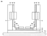
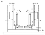
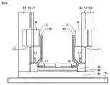
- FIG. 6 is a cross-sectional view schematically showing the configuration of the power conversion device 100. For convenience of explanation, hatching is not attached to FIG.
- FIG. 7 is a development view of the first printed circuit board module 71, the second printed circuit board module 72, and the third printed circuit board module 73 of the power conversion device 100.
- the thickness of the wiring member 86 is large, when the second printed circuit board module 72 and the third printed circuit board module 73 are bent as shown in FIG. 6 from the state shown in FIG. 7, the wiring member 86 and the joint portion 87 are bent. Cracks are likely to occur in the soldered part of the module.
- the thickness is 0. If it is less than mm, bending occurs in the Y-axis direction when the second printed circuit board module 72 and the third printed circuit board module 73 are bent perpendicularly to the first printed circuit board module 71 in the Z-axis direction. .. By deforming this bent portion in the Y-axis direction, it is possible to absorb the misalignment. Therefore, the thinner the thickness, the more the positional deviation in the Y-axis direction can be absorbed.
- the wiring member 86 is bent at a right angle and connected to the joint portion 87.
- the junction 87 is part of the circuit pattern.
- the wiring member 86 can be bent not only at a right angle but also at any angle from 0 degrees to 180 degrees.
- the second printed circuit board module 72 and the third printed circuit board module 73 can be bent in the Z-axis direction with respect to the first printed circuit board module 71. Therefore, each of the second printed circuit board module 72 and the third printed circuit board module 73 can be arranged perpendicularly to the external cooling body 21.
- the bottom area of the structure in which the first printed circuit board module 71, the second printed circuit board module 72, and the third printed circuit board module 73 are assembled is made smaller than that of the external cooling body 21, and this structure is made into the external cooling body 21. Can be implemented in.
- the direction parallel to the longitudinal direction of the wiring member 86 on the rectangular thin plate is defined as the X axis
- the direction perpendicular to the longitudinal direction is defined as the Y axis
- the direction perpendicular to the cooling surface is defined as the Z-axis direction.
- the position of the joint portion 87 may deviate from the design position in the Y-axis direction when the printed circuit board module is screwed to the cooling body.
- a misalignment in the Y-axis direction may occur. Further, in the state shown in FIG.
- the wiring member 86 can absorb the positional deviation in the Z-axis direction.
- the power conversion device 100 is manufactured through a preparation step S100, an assembly step S200, and a connection step S300.
- the electronic components including the first component, the second component, and the third component, the first printed circuit board 31, the second printed circuit board, the third printed circuit board 33, the first cooling body 51, and the second cooling body 52 ,
- the wiring member 86 is prepared.
- the printed circuit board may be divided from one board. In this case, the perforations formed on one substrate are cut by a router to be divided into each printed circuit board.
- each printed circuit board may be connected by a wiring member 86 via a joint portion 87.
- the perforations may be arranged so as not to overlap with the wiring member 86.
- the first printed circuit board module 71, the second printed circuit board module 72, and the third printed circuit board module 73 are assembled, respectively. Further, in the assembly step S200, each of the first printed circuit board module 71, the second printed circuit board module 72, and the third printed circuit board module 73 goes through an electronic component mounting step, a printed circuit board combination step, and a printed circuit board fixing step. Manufactured.
- the assembly process of the first printed circuit board module 71 will be described.
- the electronic component (first component) is mounted on the first main surface S1 of the first printed circuit board 31 by flow soldering, reflow soldering, or the like.
- the printed circuit board combination step the first cooling body 51, the first insulating member 41, and the first printed circuit board 31 on which the electronic component is mounted on the surface 31a are combined.
- the first cooling body 51 is thermally connected to the second main surface S2 facing the first main surface S1 of the first printed circuit board 31.
- the printed circuit board fixing step the first printed circuit board 31 is fixed to the first cooling body 51 by the first fixing member 61 via the first insulating member 41.
- the assembly process of the second printed circuit board module 72 will be described.
- the electronic component (second component) is mounted on the third main surface S3 of the second printed circuit board 32 by flow soldering, reflow soldering, or the like.
- the second cooling body 52, the second insulating member 42, and the second printed circuit board 32 on which the electronic component is mounted on the surface 32a are combined.
- the upper and lower cores are combined.
- the second cooling body 52 is thermally connected to the fourth main surface S4 facing the third main surface S3 of the second printed circuit board 32.
- the second printed circuit board 32 is fixed to the second cooling body 52 by the second fixing member 62 via the second insulating member 42.
- the assembly process of the third printed circuit board module 73 will be described.
- the electronic component (third component) is mounted on the fifth main surface S5 of the third printed circuit board 33 by flow soldering, reflow soldering, or the like.
- the third cooling body 53, the third insulating member 43, and the third printed circuit board 33 on which the electronic component is mounted on the surface 33a are combined.
- the upper and lower cores are combined.
- the third cooling body 53 is thermally connected to the sixth main surface S6 facing the fifth main surface S5 of the third printed circuit board 33.
- the third printed circuit board 33 is fixed to the third cooling body 53 by the third fixing member 63 via the third insulating member 43.
- the first wiring member 86a of the wiring member 86 electrically connects the first printed circuit board 31 and the second printed circuit board 32.
- the first wiring member 86a is connected to the first main surface S1 of the first printed circuit board 31 and the third main surface S3 of the second printed circuit board 32 by either direct connection or soldering joint, respectively.
- the first wiring member 86a is attached to the first printed circuit board 31. It may be electrically connected to the second printed circuit board 32.
- the first wiring member 86a is the first printed circuit board 31. And the second printed circuit board 32 may be electrically connected.
- the second wiring member 86b of the wiring member 86 electrically connects the first printed circuit board 31 and the third printed circuit board 33.
- the second wiring member 86b is connected to the first main surface S1 of the first printed circuit board 31 and the fifth main surface S5 of the third printed circuit board 33 by either direct connection or soldering joint, respectively.
- the first wiring member 86a is attached to the first printed circuit board 31. It may be electrically connected to the third printed circuit board 33.
- the first wiring member 86a is the first printed circuit board 31.
- the third printed circuit board 33 may be electrically connected.
- each of the second printed circuit board module 72 and the third printed circuit board module 73 is electrically connected to the first printed circuit board module 71 by a wiring member 86.
- the joint portion 87 is mounted on each of the first printed circuit board 31, the second printed circuit board 32, and the third printed circuit board 33.
- the wiring member 86 is electrically connected to the joint portion 87.
- each of the second printed circuit board module 72 and the third printed circuit board module 73 is electrically connected to the first printed circuit board module 71.
- the first printed circuit board 31 is connected to the second printed circuit board 32 and the third printed circuit board 33 by using the wiring member 86, but three or more boards are connected to one board. May be done.
- the joint portion 87 is a part of the circuit pattern, and is connected to the joint portion 87 by soldering without using a fastening member such as a screw and a terminal block. Further, the joint portion 87 may be connected to the joint portion 87 not only by soldering but also by welding, caulking, ultrasonic bonding or the like.
- each of the electronic component (second component) and the electronic component (third component) is fixed to the grooves G provided in each of the second printed circuit board 32 and the third printed circuit board 33.
- each of the second printed circuit board module 72 and the third printed circuit board module 73 is connected and fixed to the first printed circuit board module 71.
- the second cooling body 52 is arranged so as to extend in the direction from the second main surface S2 of the first printed circuit board 31 toward the first main surface S1.
- the third cooling body 53 is arranged so as to extend in the direction from the second main surface S2 of the first printed circuit board 31 toward the first main surface S1.
- connection step S300 the first cooling body 51 included in the first printed circuit board module 71, the second cooling body 52 included in the second printed circuit board module 72, and the third cooling body included in the third printed circuit board module 73.
- the 53 is connected and secured either directly or via other members.
- each of the second cooling body 52 and the third cooling body 53 is arranged so as to extend in the direction from the second main surface S2 of the first printed circuit board 31 toward the first main surface S1.
- the first cooling body 51 is thermally coupled to the external cooling body 21 by a method such as surface contact with the external cooling body 21.
- connection step S300 the second cooling body 52 and the third cooling body 53 are thermally connected to the first cooling body 51.
- the second cooling body 52 and the third cooling body 53 are assembled on the first cooling body 51 from the state of FIG. 7 as shown in FIG.
- the positions of the 87s and the positions of the joints 87 facing each other of the first printed circuit board 31 and the third printed circuit board 33 may be displaced. Even if the positions of the joints 87 are displaced, the connection can be maintained by the deformation of the wiring member 86.
- the electronic components are mounted not only on the first printed circuit board 31 but also on the second printed circuit board 32. Therefore, even when the number of electronic components that are high heat generation components increases, the expansion of the first cooling body 51 can be suppressed by mounting the electronic components on the second printed circuit board 32. Therefore, it is possible to suppress the expansion of the bottom area of the power conversion device 100. Further, by mounting the electronic component on the second printed circuit board 32, it is possible to shorten the heat dissipation distance in which the heat generated by the electronic component mounted on the second printed circuit board 32 is transferred to the second cooling body 52.
- the heat dissipation of the second printed circuit board 32 can be improved.
- the first wiring member 86a is connected to the first main surface S1 of the first printed circuit board 31 and the third main surface S3 of the second printed circuit board 32 by either direct connection or soldering joint, respectively. Therefore, since screws and terminal blocks are not used in the connection between the boards, the energization path is shortened by that amount, and the electric resistance is reduced. Therefore, the Joule heat generated in the screw and the terminal block is reduced, so that the temperature rise of the first wiring member 86a can be suppressed. Therefore, it is possible to suppress the temperature rise of the power conversion device 100. As a result, the power conversion device 100 according to the first embodiment can operate at a high output.
- the electronic component is also mounted on the third printed circuit board 33. Therefore, even when the number of electronic components that are high heat generation components increases, the expansion of the first cooling body 51 can be suppressed by mounting the electronic components on the third printed circuit board 33. Therefore, it is possible to suppress the expansion of the bottom area of the power conversion device 100. Further, by mounting the electronic component on the third printed circuit board 33, it is possible to shorten the heat dissipation path in which the heat generated by the electronic component mounted on the third printed circuit board 33 is transmitted to the third cooling body 53. Therefore, the heat dissipation of the third printed circuit board 33 can be improved.
- the second wiring member 86b is connected to the first main surface S1 of the first printed circuit board 31 and the fifth main surface S5 of the third printed circuit board 33 by either direct connection or soldering joint, respectively. Therefore, since screws and terminal blocks are not used in the connection between the boards, the energization path is shortened by that amount, and the electric resistance is reduced. Therefore, the Joule heat generated in the screw and the terminal block is reduced, so that the temperature rise of the second wiring member 86b can be suppressed. Therefore, it is possible to suppress the temperature rise of the power conversion device 100.
- the power conversion device 100 according to the first embodiment will be described in comparison with the comparative example.
- the terminal blocks installed at the joints 87 provided at the ends of the first printed circuit board 31 and the second printed circuit board 32 are connected by using screws and harnesses.
- the terminal block, screws, and the like installed at the joint portion 87 of the second printed circuit board 32 become the first printed circuit board 31. It interferes with the terminal block, screws, electronic parts, etc. installed at the end of the. Therefore, the first printed circuit board 31 and the second printed circuit board 32 must be mounted separately so that the components of the first printed circuit board 31 and the second printed circuit board 32 do not interfere with each other. Then, the volume and the bottom area of the power conversion device 100 become large.
- a thin ribbon-shaped copper plate is used as the wiring member 86 between the first printed circuit board 31 and the second printed circuit board 32 without using screws and terminal blocks.
- the joints 87 of the first printed circuit board 31 and the second printed circuit board 32 are connected to each other by soldering.
- the shape of the wiring member 86 has a large surface area in contact with air as compared with the circular wiring member having the same cross-sectional area. Therefore, it is possible to improve the heat dissipation of the power conversion device 100 with respect to the heat generated by the energization of the wiring member. Therefore, the current flowing through the power converter 100 can be increased. As a result, the power conversion device 100 according to the first embodiment can operate at a high output.
- the second printed circuit board 32 and the third printed circuit board 33 are arranged so as to face each other. Therefore, the power conversion device 100 can be miniaturized.
- the power conversion device 100 includes an external cooling body 21 thermally connected to the first cooling body 51.
- a heat dissipation path for radiating heat a first heat dissipation path for radiating heat to the external cooling body 21 can be formed via the first printed circuit board 31, the first insulating member 41, and the first cooling body 51.
- the heat radiated from the power conversion device 100 to the heat generated by the circuit pattern formed on the surface or the inside of the first printed circuit board 31 and the heat generated by the high heat generating component mounted on the first printed circuit board 31. Can improve sex.
- the power conversion device 100 according to the first embodiment can operate at a high output.
- the power conversion device 100 when the first insulating member 41 is brought into surface contact with the first printed circuit board 31 and the first cooling body 51, the area of the contact surface between the first insulating member 41 and the first printed circuit board 31 and the first insulation. Since the area of the contact surface between the member 41 and the first cooling body 51 can be widened, the contact thermal resistance of the contact surface between the first insulating member 41 and the first printed circuit board 31 and the first insulating member 41 and the first cooling body can be increased. The contact thermal resistance of the contact surface of 51 can be reduced, and the heat dissipation of the first heat dissipation path can be improved. As a result, the power conversion device 100 according to the first embodiment can operate at a high output.
- the second printed circuit board 32, the second insulating member 42, the second cooling body 52, and the first cooling body are used as heat dissipation paths to dissipate the heat generated by the 5e, 5f, 5g, 5h, and the transformers 3 and 4.
- a second heat dissipation path that dissipates heat to the external cooling body 21 can be formed via the 51.
- the second heat dissipation path does not include the plate-shaped substrate mounting portion as compared with the configuration described in Patent Document 1, the length of the heat dissipation path can be shortened and the heat dissipation can be improved. Therefore, the heat radiated from the power conversion device 100 to the heat generated by the circuit pattern formed on the surface or the inside of the second printed circuit board 32 and the heat generated by the high heat generating component mounted on the second printed circuit board 32. Can improve sex. As a result, the power conversion device 100 according to the first embodiment can operate at a high output.
- the power conversion device 100 when the second insulating member 42 is brought into surface contact with the second printed circuit board 32 and the second cooling body 52, the area of the contact surface between the second insulating member 42 and the second printed circuit board 32 and the second insulation Since the area of the contact surface between the member 42 and the second cooling body 52 can be widened, the contact thermal resistance of the contact surface between the second insulating member 42 and the second printed circuit board 32 and the second insulating member 42 and the second cooling body can be increased. The contact thermal resistance of the contact surface of 52 can be reduced, and the heat dissipation of the second heat dissipation path can be improved. As a result, the power conversion device 100 according to the first embodiment can operate at a high output.
- the power conversion device 100 when the lower surface of the core is in direct contact with the second cooling body 52, or the lower surface of the core is via a heat conductive member such as a heat conductive grease, a heat conductive sheet, or a heat conductive adhesive.
- a heat conductive member such as a heat conductive grease, a heat conductive sheet, or a heat conductive adhesive.
- the heat generated by the transformers 3 and 4 is transferred to the second cooling body. Since heat can be dissipated to the external cooling body 21 via the 52 and the first cooling body 51, the heat dissipation of the power conversion device 100 with respect to the heat generated by the transformers 3 and 4 can be improved. As a result, the power conversion device 100 according to the first embodiment can operate at a high output.
- the heat generated by the circuit pattern formed on the surface or the inside of the third printed circuit board 33 and the heat generated by the reactors 6 and 7, which are high heat generating components mounted on the third printed circuit board 33, are combined with each other.
- a heat dissipation path a third heat dissipation path that dissipates heat to the external cooling body 21 can be formed via the third printed circuit board 33, the third insulating member 43, the third cooling body 53, and the first cooling body 51. .. Since the third heat dissipation path does not include the plate-shaped substrate mounting portion as compared with the configuration described in Patent Document 1, the length of the heat dissipation path can be shortened and the heat dissipation can be improved.
- the heat radiated from the power conversion device 100 to the heat generated by the circuit pattern formed on the surface or the inside of the third printed circuit board 33 and the heat generated by the high heat generating component mounted on the third printed circuit board 33. Can improve sex.
- the power conversion device 100 according to the first embodiment can operate at a high output.
- the power conversion device 100 when the third insulating member 43 is brought into surface contact with the third printed circuit board 33 and the third cooling body 53, the area of the contact surface between the third insulating member 43 and the third printed circuit board 33 and the third insulation. Since the area of the contact surface between the member 43 and the third cooling body 53 can be widened, the contact thermal resistance of the contact surface between the third insulating member 43 and the third printed circuit board 33 and the third insulating member 43 and the third cooling body can be increased. The contact thermal resistance of the contact surface of 53 can be reduced, and the heat dissipation of the third heat dissipation path can be improved. As a result, the power conversion device 100 according to the first embodiment can operate at a high output.
- the power conversion device 100 when the lower surface of the core is in direct contact with the third cooling body 53, or the lower surface of the core is via a heat conductive member such as a heat conductive grease, a heat conductive sheet, or a heat conductive adhesive.
- a heat conductive member such as a heat conductive grease, a heat conductive sheet, or a heat conductive adhesive.
- the heat generated by the reactors 6 and 7 is transferred to the third cooling body. Since heat can be dissipated to the external cooling body 21 via the 53 and the first cooling body 51, the heat dissipation of the power conversion device 100 with respect to the heat generated by the reactors 6 and 7 can be improved. As a result, the power conversion device 100 according to the first embodiment can operate at a high output.
- the power conversion device 100 can operate at a high output.
- the thickness of the first cooling body 51 in the direction substantially perpendicular to the surface 31a of the first printed circuit board 31 is thin.
- the lengths of the first heat dissipation path, the second heat dissipation path, and the third heat dissipation path can be shortened, so that the heat dissipation property can be improved.
- the thickness of the second cooling body 52 in the direction substantially perpendicular to the surface 32a of the second printed circuit board 32 is increased.
- the thermal resistance of the second cooling body 52 included in the second heat dissipation path can be reduced, so that the heat dissipation can be improved.
- the thickness of the third cooling body 53 in the direction substantially perpendicular to the surface 33a of the third printed circuit board 33 is increased.
- the thermal resistance of the third cooling body 53 included in the third heat dissipation path can be reduced, so that the heat dissipation can be improved.
- the first cooling body 51 can be thermally connected to the first printed circuit board 31 via the first insulating member 41.
- the second cooling body 52 can be thermally connected to the second printed circuit board 32 via the second insulating member 42.
- the third cooling body 53 can be thermally connected to the third printed circuit board 33 via the third insulating member 43.
- the second cooling body 52 is thermally connected to the first cooling body 51
- the third cooling body 53 is thermally connected to the first cooling body 51. Has been done. Therefore, the heat generated by the electronic components mounted on the second printed circuit board 32 can be dissipated from the first cooling body 51 via the second cooling body 52, and the electronic components mounted on the third printed circuit board 33 can be dissipated. The heat generated in the above can be dissipated from the first cooling body 51 via the third cooling body 53.
- the first cooling body 51 is thermally connected to each of the second cooling body 52 and the third cooling body 53 via the first heat conductive member HC1. ing. Therefore, the heat transfer efficiency from the second cooling body 52 to the first cooling body 51 can be improved by the first heat conductive member HC1, and the heat transfer efficiency from the third cooling body 53 to the first cooling body 51 can be improved. Can be improved.
- the wiring member 86 has a thickness of 0.05 mm or more and less than 0.3 mm, and has a current density of 50 A / mm 2 or more and 100 / mm 2 or more. Therefore, the thin wiring member 86 can be energized with a large current.
- the manufacturing method of the power conversion device 100 includes a preparation step S100, an assembly step S200, and a connection step S300. Therefore, the first cooling body 51 constituting the bottom surface of the support, the second cooling body 52 and the third cooling body 53 forming the side surfaces of the support, the first insulating member 41, the second insulating member 42, and the third The work of arranging the insulating member 43 and fixing the first printed circuit board 31, the second printed circuit board 32, and the third printed circuit board 33, and the first printed circuit board module 71, the second printed circuit board module 72, and the third printed circuit board module 73. It is no longer necessary to perform the work of electrically connecting the spaces in a space that is roughly enclosed. As a result, it is not necessary to design the heat in consideration of the thickness variation of the first insulating member 41, the second insulating member 42, and the third insulating member 43 due to the poor workability.
- the second cooling body 52 is arranged so as to extend from the second main surface S2 of the first printed circuit board 31 toward the first main surface S1.
- the first wiring member 86a electrically connects the first printed circuit board 31 and the second printed circuit board 32.
- the first wiring member 86a is connected to the first main surface S1 of the first printed circuit board 31 and the third main surface S3 of the second printed circuit board 32 by either direct connection or soldering joint, respectively. Therefore, the power conversion device 100 can be miniaturized, the heat dissipation can be improved, and the temperature rise of the power conversion device 100 can be suppressed.
- the switching elements 2a, 2b, 2c, and 2d which are high heat generating components, are arranged in the first printed circuit board module 71.
- the high heat generation component can reduce the thermal resistance to the external cooling body. Therefore, the power conversion device 100 can be miniaturized, the heat dissipation can be improved, and the temperature rise of the power conversion device 100 can be suppressed.
- the third cooling body 53 is arranged so as to extend in the direction from the second main surface S2 of the first printed circuit board 31 toward the first main surface S1.
- the second wiring member 86b electrically connects the first printed circuit board 31 and the third printed circuit board 33.
- the second wiring member 86b is connected to the first main surface S1 of the first printed circuit board 31 and the fifth main surface S5 of the third printed circuit board 33 by either direct connection or soldering joint, respectively. Therefore, the power conversion device 100 can be miniaturized, the heat dissipation can be improved, and the temperature rise of the power conversion device 100 can be suppressed.
- the second cooling body 52 and the third cooling body 53 are thermally connected to the first cooling body 51. Therefore, the power conversion device 100 can be miniaturized, the heat dissipation can be improved, and the temperature rise of the power conversion device 100 can be suppressed.
- an electronic component (second component) and an electronic component (second component) are formed in the grooves G provided in each of the second printed circuit board 32 and the third printed circuit board 33.
- Each of the electronic components (third component) is fixed. Therefore, the power conversion device 100 can be miniaturized, the heat dissipation can be improved, and the temperature rise of the power conversion device 100 can be suppressed. Further, the electronic component can be securely fixed.
- the power conversion device 100 according to the modified example of the first embodiment will be described.
- the modified example of the first embodiment has the same configuration, operation, and effect as that of the first embodiment. Therefore, the same components as those in the first embodiment are designated by the same reference numerals, and the description thereof will not be repeated.
- FIG. 9 is a cross-sectional view showing a state after the first cooling body 51, the second cooling body 52, and the third cooling body 53 are assembled as shown in FIG. Note that hatching is not attached to FIG. 9 for convenience of explanation.
- the power conversion device 100 according to the first modification of the first embodiment basically has the same configuration as the power conversion device 100 according to the first embodiment.
- the power conversion device 100 according to the first modification of the first embodiment has a different shape of the wiring member 86 than the power conversion device 100 according to the first embodiment.
- the shape of the wiring member 86 is on a straight line.
- the wiring member 86 is preliminarily folded so that the wiring member 86 is bent a plurality of times.
- the wiring member 86 is configured in a bellows shape having a plurality of bent portions BP. That is, the wiring member 86 has a plurality of bent portions BP. Of the plurality of bent portions BP, the adjacent bent portion BPs are arranged so as to overlap each other.
- the effect of the power conversion device 100 according to the first modification of the first embodiment will be described.
- the wiring member 86 since the wiring member 86 has a plurality of bent portions BP, the wiring member 86 is miniaturized by being folded. Further, among the plurality of bent portions BP, the adjacent bent portion BPs are arranged so as to overlap each other. Therefore, when the wiring member 86 is bent, the mountain and the mountain of the bent wiring member 86 overlap each other, and the energization path of the wiring member 86 becomes short. As a result, the electric resistance of the wiring member 86 is further reduced, so that heat generation can be reduced. As a result, the power conversion device 100 according to the first modification of the first embodiment can operate at a high output.
- the power conversion device 100 according to the second modification of the first embodiment will be described with reference to FIGS. 10 and 11. Note that hatching is not attached to FIG. 11 for convenience of explanation.
- the power conversion device 100 according to the second modification of the first embodiment basically has the same configuration as the power conversion device 100 according to the first embodiment.
- the power conversion device 100 according to the second modification of the first embodiment has a different shape of the wiring member 86 than the power conversion device 100 according to the first embodiment.
- the wiring member 86 is preliminarily bent in an arch shape in the positive direction of the Z axis.
- the structure has a space in the lower center of the wiring member 86.
- the wiring member 86 has a shape bent so as to be adjacent to the joint portions 87 at both ends of the wiring member 86. Then, the component can be installed in the space at the lower center of the wiring member 86 that is bent in the positive direction of the Z axis.
- the center of the wiring member 86 bulges in an arc shape and has a shape facing the joint portion 87 of the wiring member 86, and the two bending portions CP provided on the wiring member 86 are close to each other.
- the bent portion CP of the wiring member 86 is provided so as to be adjacent to the end portions of the first printed circuit board 31, the second printed circuit board 32, and the third printed circuit board 33, and even if the bent portion CP of the wiring member 86 comes into contact with each other. good.
- the contact between the bent portions CP of the wiring member 86 shortens the energization path when the printed circuit board modules are brought close to each other.
- the wiring member 86 faces the joint portion 87 by the center of the wiring member 86 bulging in an arch shape.
- the contact between the two bent portions CP provided on the wiring member 86 shortens the energization path.
- the electric resistance of the wiring member 86 is reduced, so that heat generation can be reduced.
- the power conversion device 100 according to the second modification of the first embodiment can operate at a high output.
- the power conversion device 100 according to the third modification of the first embodiment basically has the same configuration as the power conversion device 100 according to the first embodiment.
- the power conversion device 100 according to the third modification of the first embodiment has a first cooling body 51, a second cooling body 52, and a third cooling body 53 as compared with the power conversion device 100 according to the first embodiment.
- the arrangement of is different.
- the first cooling body 51 is arranged so as to be sandwiched between the second cooling body 52 and the third cooling body 53.
- the power conversion device 100 according to the modified example 4 of the first embodiment will be described with reference to FIG.
- the power conversion device 100 according to the fourth modification of the first embodiment basically has the same configuration as the power conversion device 100 according to the first embodiment.
- the power conversion device 100 according to the fourth modification of the first embodiment has a different configuration of the first cooling body 51 and the external cooling body 21 than the power conversion device 100 according to the first embodiment.
- the first cooling body 51 is integrally formed with the external cooling body 21.
- the first cooling body 51 also serves as the external cooling body 21.
- the first cooling body 51 is thermally coupled to the external cooling body 21 by a method such as integrally forming with the external cooling body 21.
- the power conversion device 100 according to the modified example 5 of the first embodiment will be described with reference to FIG.
- the power conversion device 100 according to the fifth modification of the first embodiment basically has the same configuration as the power conversion device 100 according to the first embodiment.
- the power conversion device 100 according to the fifth modification of the first embodiment has a different arrangement of the second printed circuit board module 72 than the power conversion device 100 according to the first embodiment.
- the second printed circuit board module 72 and the third printed circuit board module 73 are arranged so as to be adjacent to each other.
- the second printed circuit board 32 and the third printed circuit board 33 are arranged so as to be adjacent to each other.
- the second printed circuit board 32 and the third printed circuit board 33 are arranged so as to be adjacent to each other. Therefore, the power conversion device 100 can be miniaturized.
- the power conversion device 100 according to the modification 6 of the first embodiment will be described with reference to FIG.
- the power conversion device 100 according to the sixth modification of the first embodiment basically has the same configuration as the power conversion device 100 according to the first embodiment.
- the power conversion device 100 according to the sixth modification of the first embodiment is different from the power conversion device 100 according to the first embodiment in that the third printed circuit board module 73 is not arranged.
- the power conversion device 100 according to the sixth modification of the first embodiment does not have the third printed circuit board module 73.
- Embodiment 2 the power conversion device 100 according to the second embodiment will be described with reference to FIG.
- the second embodiment has the same configuration, operation, and effect as the first embodiment, unless otherwise specified. Therefore, the same components as those in the first embodiment are designated by the same reference numerals, and the description thereof will not be repeated.
- the power conversion device 100 according to the second embodiment basically has the same configuration as the power conversion device 100 according to the first embodiment.
- the power conversion device 100 according to the second embodiment is different from the power conversion device 100 according to the first embodiment in that it includes a fourth cooling body 54 and a fifth cooling body 55.
- the fourth cooling body 54 is configured to extend vertically with the surface connected to the surface 51a of the first cooling body 51 as the bottom surface.
- the fourth cooling body 54 extends from the second main surface S2 of the first printed circuit board 31 toward the first main surface S1.
- the fifth cooling body 55 is configured to extend vertically with the surface connected to the surface 51a of the first cooling body 51 as the bottom surface.
- the fifth cooling body 55 extends from the second main surface S2 of the first printed circuit board 31 toward the first main surface S1.
- Each of the fourth cooling body 54 and the fifth cooling body 55 cools at least one of the first cooling body 51, the second cooling body 52, and the third cooling body 53 directly or via other members. Connected and secured to the body.
- Each of the fourth cooling body 54 and the fifth cooling body 55 is thermally connected to each of the first cooling body 51, the second cooling body 52, and the third cooling body 53.
- the fourth cooling body 54 is thermally connected to the first cooling body 51, the second cooling body 52, and the third cooling body 53.
- the fifth cooling body 55 is thermally connected to the first cooling body 51, the second cooling body 52, and the third cooling body 53.
- a heat conductive member such as a heat conductive adhesive (second heat conductive member) HC2 may be arranged.
- the heat conductive member (second heat conductive member) HC2 contains at least one of a heat conductive grease, a heat conductive sheet and a heat conductive adhesive.
- the fourth cooling body 54 is thermally connected to each of the first cooling body 51, the second cooling body 52, and the third cooling body 53 via a heat conductive member (second heat conductive member) HC2.
- the fifth cooling body 55 is thermally connected to each of the first cooling body 51, the second cooling body 52, and the third cooling body 53 via a heat conductive member (second heat conductive member) HC2.
- Each of the fourth cooling body 54 and the fifth cooling body 55 constitutes a side surface of the support of the power conversion device 100.
- the power conversion device 100 according to the second embodiment can obtain the same effect as the power conversion device 100 according to the first embodiment.
- the second printed circuit board 32, the second insulating member 42, the second cooling body 52, and the first cooling are used as heat dissipation paths to dissipate the heat generated by the 5e, 5f, 5g, 5h and the transformers 3 and 4.
- the first is heat dissipation to the external cooling body 21 via the second printed circuit board 32, the second insulating member 42, the second cooling body 52, the fourth cooling body 54, and the first cooling body 51. It is a route.
- the second is heat dissipation to the external cooling body 21 via the second printed circuit board 32, the second insulating member 42, the second cooling body 52, the fifth cooling body 55, and the first cooling body 51. It is a route.
- the following two heat dissipation paths are formed.
- the first is heat dissipation to the external cooling body 21 via the third printed circuit board 33, the third insulating member 43, the third cooling body 53, the fourth cooling body 54, and the first cooling body 51. It is a route.
- the second is heat dissipation to the external cooling body 21 via the third printed circuit board 33, the third insulating member 43, the third cooling body 53, the fifth cooling body 55, and the first cooling body 51. It is a route. Therefore, the heat radiated from the power conversion device 100 to the heat generated by the circuit pattern formed on the surface or the inside of the third printed circuit board 33 and the heat generated by the high heat generating component mounted on the third printed circuit board 33. It can enhance the sex. As a result, the power conversion device 100 according to the second embodiment can operate at a high output.
- the fourth cooling body 54 includes each of the first cooling body 51, the second cooling body 52, and the third cooling body 53 and a heat conductive member (second heat conductivity). Member) It is thermally connected via HC2.
- the fifth cooling body 55 is thermally connected to each of the first cooling body 51, the second cooling body 52, and the third cooling body 53 via a heat conductive member (second heat conductive member) HC2. Therefore, the second heat conductive member HC2 can improve the heat transfer efficiency from the fourth cooling body 54 to the first cooling body 51, the second cooling body 52, and the third cooling body 53, and the fifth cooling body. It is possible to improve the heat transfer efficiency from 55 to the first cooling body 51, the second cooling body 52, and the third cooling body 53.
- the power conversion device 100 is configured such that the first cooling body 51 is arranged so as to be sandwiched between the fourth cooling body 54 and the fifth cooling body 55. You may.
- Embodiment 3 Next, the power conversion device 100 according to the third embodiment will be described with reference to FIGS. 18 and 19. Unless otherwise specified, the third embodiment has the same configuration, operation, and effect as the second embodiment. Therefore, the same components as those in the second embodiment are designated by the same reference numerals, and the description thereof will not be repeated.
- the power conversion device 100 according to the third embodiment basically has the same configuration as the power conversion device 100 according to the second embodiment.
- the power conversion device 100 according to the third embodiment is different from the power conversion device 100 according to the second embodiment in that it includes a fourth printed circuit board module 74 and a fifth printed circuit board module 75.
- the fourth printed circuit board module 74 includes a fourth printed circuit board 34, a fourth insulating member 44, a fourth cooling body 54, a fourth fixing member 64, an electronic component, and a wiring member 86.
- the fourth printed circuit board (fourth board) 34 has a front surface (seventh main surface) S7 on which electronic components (fourth components) are mounted and a back surface (eighth main surface) S8 facing the fourth cooling body 54. have.
- the seventh main surface S7 faces the eighth main surface S8.
- the fourth insulating member 44 is arranged between the eighth main surface S8 of the fourth printed circuit board 34 and the fourth cooling body 54.
- the fourth cooling body 54 is thermally connected to the eighth main surface S8 of the fourth printed circuit board 34.
- the fourth cooling body 54 is thermally connected to the eighth main surface S8 of the fourth printed circuit board 34 via the fourth insulating member 44.
- the fourth cooling body 54 is configured to extend vertically with the surface connected to the surface 51a of the first cooling body 51 facing the first printed circuit board 31 as the bottom surface.
- the fourth cooling body 54 extends from the second main surface S2 of the first printed circuit board 31 toward the first main surface S1.
- the fourth cooling body 54 is thermally connected to each of the first cooling body 51, the second cooling body 52, and the third cooling body 53.
- the fourth fixing member 64 is configured to fix the fourth printed circuit board 34 to the fourth cooling body 54.
- the fifth printed circuit board module 75 includes a fifth printed circuit board 35, a fifth insulating member 45, a fifth cooling body 55, a fifth fixing member 65, and electronic components.
- the fifth printed circuit board (fifth board) 35 has a front surface (9th main surface) S9 on which electronic components (fifth component) are mounted and a back surface (10th main surface) S10 facing the fifth cooling body 55. have.
- the ninth main surface S9 faces the tenth main surface S10.
- the fifth insulating member 45 is arranged between the tenth main surface S10 of the fifth printed circuit board 35 and the fifth cooling body 55.
- the fifth cooling body 55 is thermally connected to the tenth main surface S10 of the fifth printed circuit board 35.
- the fifth cooling body 55 is thermally connected to the tenth main surface S10 of the fifth printed circuit board 35 via the fifth insulating member 45.
- the fifth cooling body 55 is configured to extend vertically with the surface connected to the surface 51a of the first cooling body 51 facing the first printed circuit board 31 as the bottom surface.
- the fifth cooling body 55 extends from the second main surface S2 of the first printed circuit board 31 toward the first main surface S1.
- the fifth cooling body 55 is thermally connected to each of the first cooling body 51, the second cooling body 52, and the third cooling body 53.
- the fifth fixing member 65 is configured to fix the fifth printed circuit board 35 to the fifth cooling body 55.
- a joint portion 87 is provided on each of the 4th printed circuit board 34 and the 5th printed circuit board 35.
- the first printed circuit board 31 and the fourth printed circuit board 34, and the first printed circuit board 31 and the fifth printed circuit board 35 are electrically connected to each other at the joint portion 87 by the wiring member 86, respectively.
- the fourth printed circuit board module 74 and the fifth printed circuit board module 75 also have the same preparation process, assembly process, and connection process as those in the first embodiment.
- a joint portion 87 is provided on the second printed circuit board 32 and the fourth printed circuit board 34, and the third printed circuit board 33 and the fourth printed circuit board 34, respectively. It is provided.
- the second printed circuit board 32 and the fourth printed circuit board 34, and the third printed circuit board 33 and the fourth printed circuit board 34 are electrically connected to each other at the joint portion 87 by the wiring member 86, respectively.
- the second printed circuit board 32 and the fifth printed circuit board 35, and the third printed circuit board 33 and the fifth printed circuit board 35 may be electrically connected to each other at the joint portion 87 by the wiring member 86, respectively.
- the shape of the wiring member 86 connecting the second printed circuit board 32 and the fourth printed circuit board 34, and the third printed circuit board 33 and the fourth printed circuit board 34 is an L-shape in FIG. 19, but is limited to this. Not done.
- the shape of the wiring member 86 is such that when the second printed circuit board 32 and the fourth printed circuit board 34 are bent in the Z-axis direction with respect to the first printed circuit board 31, the Z of the second printed circuit board 32 and the fourth printed circuit board 34 Any shape may be used as long as the axial misalignment can be alleviated.
- the shape of the wiring member 86 is such that the third printed circuit board 33 and the fourth printed circuit board 34 are bent in the Z-axis direction when the third printed circuit board 33 and the fourth printed circuit board 34 are bent with respect to the first printed circuit board 31. Any shape may be used as long as the misalignment in the Z-axis direction can be alleviated.
- the second printed circuit board 32 and the third printed circuit board 33 may be electrically connected.
- the wiring member 86 includes the third wiring member 86c.
- the third wiring member 86c electrically connects the second printed circuit board 32 and the third printed circuit board 33.
- the third wiring member 86c is connected to the third main surface S3 of the second printed circuit board 32 and the fifth main surface S5 of the third printed circuit board 33 by either direct connection or solder bonding, respectively.
- the effect of the power conversion device 100 according to the third embodiment will be described.
- the second printed circuit board 32 when the second printed circuit board 32 is energized to the fourth printed circuit board 34, the second printed circuit board 32 can be directly energized without passing through the first printed circuit board 31. Therefore, the energization path of the fourth printed circuit board 34 becomes the shortest, and the energization pattern of the first printed circuit board can be omitted. As a result, the electric resistance of the energization pattern is reduced, so that heat generation can be reduced. Further, since the area of the first printed circuit board 31 can be reduced, the size of the first printed circuit board 31 can be reduced. As a result, the power conversion device 100 according to the third embodiment can operate at a high output.
- the power conversion device 100 when the third printed circuit board 33 is energized to the fourth printed circuit board 34, the energization path from the third printed circuit board 33 to the fourth printed circuit board 34 is the shortest because the electric power can be directly applied without passing through the first printed circuit board 31. Moreover, the energization pattern of the first printed circuit board can be omitted. As a result, the electric resistance of the energization pattern is reduced, so that heat generation can be reduced. Further, since the area of the first printed circuit board 31 can be reduced, the size of the first printed circuit board 31 can be reduced. As a result, the power conversion device 100 according to the third embodiment can operate at a high output.
- the power conversion device 100 according to the third embodiment can obtain the same effect as the power conversion device 100 according to the second embodiment. Further, in the power conversion device 100 according to the third embodiment, the heat generated by the circuit pattern formed on the surface or the inside of the fourth printed circuit board 34 and the high heat generation component mounted on the fourth printed circuit board 34 are used. The heat generated by the smoothing capacitor 8 and the reactor 6 is radiated through the fourth printed circuit board 34, the fourth insulating member 44, the fourth cooling body 54, and the first cooling body 51 as a heat dissipation path. Therefore, a fourth heat dissipation path that dissipates heat to the external cooling body 21 can be formed.
- the fourth heat dissipation path does not include the plate-shaped substrate mounting portion as compared with the configuration described in Patent Document 1, the length of the heat dissipation path can be shortened, so that the heat dissipation can be improved. Therefore, the heat radiated from the power conversion device 100 to the heat generated by the circuit pattern formed on the surface or the inside of the fourth printed circuit board 34 and the heat generated by the high heat generating component mounted on the fourth printed circuit board 34. Can improve sex. As a result, the power conversion device 100 according to the third embodiment can operate at a high output.
- the fourth insulating member 44 when the fourth insulating member 44 is brought into surface contact with the fourth printed circuit board 34 and the fourth cooling body 54, the area of the contact surface between the fourth insulating member 44 and the fourth printed circuit board 34 and the fourth.
- the area of the contact surface between the insulating member 44 and the fourth cooling body 54 can be increased. Therefore, the contact thermal resistance of the contact surface between the fourth insulating member 44 and the fourth printed circuit board 34 and the contact thermal resistance of the contact surface between the fourth insulating member 44 and the fourth cooling body 54 can be reduced.
- the heat dissipation of the fourth heat dissipation path can be improved. As a result, the power conversion device 100 according to the third embodiment can operate at a high output.
- the fifth heat dissipation path for radiating the generated heat is radiated to the external cooling body 21 via the fifth printed circuit board 35, the fifth insulating member 45, the fifth cooling body 55, and the first cooling body 51. Can form a path. Since the fifth heat dissipation path does not include the plate-shaped substrate mounting portion as compared with the configuration described in Patent Document 1, the length of the heat dissipation path can be shortened, so that the heat dissipation can be improved.
- the heat radiated from the power conversion device 100 to the heat generated by the circuit pattern formed on the surface or the inside of the fifth printed circuit board 35 and the heat generated by the high heat generating component mounted on the fifth printed circuit board 35. Can improve sex.
- the power conversion device 100 according to the third embodiment can operate at a high output.
- the power conversion device 100 can operate at a high output.
- the thickness of the fourth cooling body 54 in the direction substantially perpendicular to the surface 34a of the fourth printed circuit board 34 is increased.
- the thermal resistance of the fourth cooling body 54 included in the fourth heat dissipation path can be reduced, so that the heat dissipation can be improved.
- the thickness of the fifth cooling body 55 in the direction substantially perpendicular to the surface 35a of the fifth printed circuit board 35 is increased.
- the thermal resistance of the fifth cooling body 55 included in the fifth heat dissipation path can be reduced, so that the heat dissipation can be improved.
- the power conversion device 100 can operate at a high output.
- the power conversion device 100 according to the third embodiment can be miniaturized.
- the power conversion device 100 may not include the fifth printed circuit board 35, the fifth insulating member 45, and the fifth fixing member 65.
- the power conversion device 100 includes an external cooling body 21, a first printed circuit board module 71, a second printed circuit board module, a third printed circuit board module 73, a fourth printed circuit board module 74, and a fifth printed circuit board module 55. You may be prepared.
- the first printed circuit board module 71, the second printed circuit board module 72, the third printed circuit board module 73, and the fourth printed circuit board module 74 are electrically connected by a wiring member 86 at a joint portion 87.
- the electronic components arranged in the first printed circuit board module 71, the second printed circuit board module 72, the third printed circuit board module 73, the fourth printed circuit board module 74, and the fifth printed circuit board module 75 may be replaced, but the first It is particularly preferable that high heat generation components are arranged on the printed circuit board module 71.
- the third wiring member 86c is directly connected to and soldered to the third main surface S3 of the second printed circuit board 32 and the fifth main surface S5 of the third printed circuit board 33, respectively. It is connected by one of the joints. As a result, the power conversion device 100 can be miniaturized.
- FIG. 21 is a cross-sectional view showing a state after the first cooling body 51, the second cooling body 52, and the third cooling body 53 are assembled as shown in FIG. For convenience of explanation, hatching is not attached to FIG. 21.
- the first printed circuit board 31 is provided with a through hole TH that penetrates the first main surface S1 and the second main surface S2.
- the second printed circuit board 32 is provided with a through hole TH that penetrates the third main surface S3 and the fourth main surface S4.
- the third printed circuit board 33 is provided with a through hole TH that penetrates the fifth main surface S5 and the sixth main surface S6.
- the inner wall of the through hole made in the printed circuit board is plated with copper having a thickness of several tens of ⁇ m.
- the material of the through hole TH is the same as that of a circuit pattern (not shown).
- the material of the through-hole TH may be the same as or different from the circuit pattern (not shown).
- the through hole TH may have the same potential as the wiring member 86 via the joint portion 87.
- the through-hole TH is insulated from the first cooling body 51, the second cooling body 52, and the third cooling body 53 by the first insulating member 41, the second insulating member 42, and the third insulating member 43, respectively.
- the through hole TH may be arranged at least directly under the joint portion (first joint portion) 87. Further, if the through holes TH are arranged not only directly under the joint portion 87 but also around the joint portion 87, the heat dissipation property is improved.
- the heat generated by the wiring member 86 is mainly dissipated through the joint portion 87, the printed circuit board, the insulating member, and the cooling body. Since the thermal resistance of the printed circuit board is the largest in the heat dissipation path of the wiring member 86, it is necessary to reduce the thermal resistance of the printed circuit board.
- the through-hole TH increases the thermal conductivity in the thickness direction of the printed circuit board directly under the joint portion 87. This reduces the thermal resistance of the printed circuit board in the thickness direction. Therefore, it is possible to improve the heat dissipation of the heat generated by the wiring member 86.
- FIG. 22 is a development view of the first printed circuit board module 71, the second printed circuit board module 72, and the third printed circuit board module 73 of the power conversion device 100.
- the surface of the wiring member 86 is covered with the insulating coating 86X.
- the material of the insulating coating 86X is, for example, vinyl chloride, fluororesin, polyimide, or the like.
- the bent wiring member 86 is an unintended location such as surrounding electronic components, a cooling body, and a circuit pattern. There is a risk of short circuit due to contact with.
- the wiring member 86 since the wiring member 86 is in contact with air, there is a path for radiating heat directly from the wiring member 86 to the air in addition to the path for radiating heat to the cooling body via the printed circuit board. However, since the wiring member 86 is made of metal, the emissivity of the surface of the wiring member 86 is low. Therefore, the radioactivity to the air is low.
- the power conversion device 100 it is possible to prevent the occurrence of a short circuit even if the wiring member 86 comes into contact with surrounding electronic components or the like when the wiring member 86 is bent by the insulating coating 86X. Further, since the emissivity of the surface of the wiring member 86 can be improved by the insulating coating 86X, the heat dissipation to the air can be improved.
- FIG. 23 is a cross-sectional view showing a state after the first cooling body 51, the second cooling body 52, and the third cooling body 53 are assembled as shown in FIG. For convenience of explanation, hatching is not attached to FIG. 23.
- the shape of the wiring member 86 is different from that of the power conversion device 100 according to the first embodiment.
- the wiring member 86 is in contact with the core K via the heat radiating member Q in a bent state. ..
- the core K is a member constituting the transformers 3 and 4 or the reactors 6 and 7.
- the heat generated by the wiring member 86 is transferred to the heat radiating member Q, the core K, the second cooling body 52, and the third cooling body 53 and radiated.
- the heat radiating member Q is made of a material having electrical insulation and good thermal conductivity.
- an adhesive having electrical insulation is used as the heat radiating member Q.
- a sheet or grease in which particles such as aluminum oxide or aluminum nitride having good thermal conductivity and electrical insulation are mixed with the silicone resin may be used.
- the length of the wiring member 86 may become long. At this time, the electric resistance value of the wiring member 86 increases and the heat dissipation path of the wiring member 86 becomes long, so that the temperature rise of the wiring member 86 increases.
- the wiring member 86 is in contact with the core K via the heat dissipation member Q in a bent state.
- the central portion of the wiring member 86 in contact with the core K can dissipate heat from the core K to the cooling body in addition to the path dissipated to the cooling body through the joint portion 87 and the path dissipated to the air. Therefore, the heat dissipation can be further improved.
- the power conversion device 100 according to the modified example of the sixth embodiment will be described.
- the modified example of the sixth embodiment has the same configuration, operation, and effect as that of the sixth embodiment. Therefore, the same components as those in the sixth embodiment are designated by the same reference numerals, and the description thereof will not be repeated.
- the power conversion device 100 according to the first modification of the sixth embodiment will be described with reference to FIG. 24.
- hatching is not attached to FIG. 24.
- the wiring member 86 may come into contact with a structure other than the core K to dissipate heat. As shown in FIG. 24, the wiring member 86 may contact the sheet metal AL fixing the core K to dissipate heat.
- the core K is fixed by the screw N and the sheet metal AL.
- Each of the second printed circuit board 32 and the third printed circuit board 33 is provided with a hole through which the screw N passes. The screw N is fixed to each of the second cooling body 52 and the third cooling body 53 through the through hole.
- the object in contact with the wiring member 86 is insulated, for example, the circuit patterns of the first cooling body 51, the second cooling body 52, the third cooling body 53, the first printed circuit board 31, and the printed circuit board (FIG.
- the object that the wiring member 86 comes into contact with, such as (not shown), is free.
- the power conversion device 100 According to the power conversion device 100 according to the first modification of the sixth embodiment, it is possible to improve the heat dissipation of the heat generated by the wiring member 86.
- the power conversion device 100 according to the second modification of the sixth embodiment will be described with reference to FIG. 25.
- hatching is not attached to FIG. 25.
- a part of the wiring member 86 may come into contact with each other to shorten the energization path.
- the energization path of the wiring member 86 is shortened. As a result, the electric resistance of the wiring member 86 is further reduced, so that heat generation can be reduced.
- 21 external cooling body 31 1st printed circuit board, 32 2nd printed circuit board, 33 3rd printed circuit board, 34 4th printed circuit board, 35 5th printed circuit board, 41-45 1st insulating member-5th insulating member, 51- 55 1st cooler to 5th cooler, 61 to 65 1st fixing member to 5th fixing member, 71 to 75 1st printed circuit board module to 5th printed circuit board module, 86 wiring member, 86a 1st wiring member, 86b 2nd wiring member, 86c 3rd wiring member, 87 joint part, 100 power conversion device, BP bent part, CP bent part, HC1 1st heat conductive member, HC2 2nd heat conductive member, S1 to S10 1st main Surface to 10th main surface, S100 preparation process, S200 assembly process, S300 connection process.
Landscapes
- Engineering & Computer Science (AREA)
- Microelectronics & Electronic Packaging (AREA)
- Power Engineering (AREA)
- Physics & Mathematics (AREA)
- Thermal Sciences (AREA)
- Manufacturing & Machinery (AREA)
- Dc-Dc Converters (AREA)
- Cooling Or The Like Of Electrical Apparatus (AREA)
- Inverter Devices (AREA)
Priority Applications (2)
| Application Number | Priority Date | Filing Date | Title |
|---|---|---|---|
| JP2022524515A JP7566020B2 (ja) | 2020-05-21 | 2021-05-19 | 電力変換装置 |
| US17/916,854 US12133369B2 (en) | 2020-05-21 | 2021-05-19 | Power conversion device |
Applications Claiming Priority (2)
| Application Number | Priority Date | Filing Date | Title |
|---|---|---|---|
| JP2020-088943 | 2020-05-21 | ||
| JP2020088943 | 2020-05-21 |
Publications (1)
| Publication Number | Publication Date |
|---|---|
| WO2021235485A1 true WO2021235485A1 (ja) | 2021-11-25 |
Family
ID=78707880
Family Applications (1)
| Application Number | Title | Priority Date | Filing Date |
|---|---|---|---|
| PCT/JP2021/018982 Ceased WO2021235485A1 (ja) | 2020-05-21 | 2021-05-19 | 電力変換装置および電力変換装置の製造方法 |
Country Status (3)
| Country | Link |
|---|---|
| US (1) | US12133369B2 (https=) |
| JP (1) | JP7566020B2 (https=) |
| WO (1) | WO2021235485A1 (https=) |
Cited By (1)
| Publication number | Priority date | Publication date | Assignee | Title |
|---|---|---|---|---|
| JP2024003916A (ja) * | 2022-06-28 | 2024-01-16 | 三菱電機株式会社 | 電力変換装置 |
Families Citing this family (2)
| Publication number | Priority date | Publication date | Assignee | Title |
|---|---|---|---|---|
| JP7595757B2 (ja) * | 2021-05-11 | 2024-12-06 | 三菱電機株式会社 | 電力変換装置 |
| US12439543B2 (en) * | 2022-09-14 | 2025-10-07 | AA Power Inc. | Power supply cooling structure |
Citations (6)
| Publication number | Priority date | Publication date | Assignee | Title |
|---|---|---|---|---|
| JPH05145208A (ja) * | 1991-11-18 | 1993-06-11 | Toshiba Corp | 回路ユニツト |
| JP3086623B2 (ja) * | 1995-04-27 | 2000-09-11 | 三洋電機株式会社 | 空気調和機 |
| JP2008305949A (ja) * | 2007-06-07 | 2008-12-18 | Nec Computertechno Ltd | 放熱機構、放熱方法 |
| JP2009165327A (ja) * | 2008-01-10 | 2009-07-23 | Mitsubishi Electric Corp | インバータ装置及びその製造方法 |
| JP2010010468A (ja) * | 2008-06-27 | 2010-01-14 | Kokusan Denki Co Ltd | 車載用電力制御装置 |
| JP2010187504A (ja) * | 2009-02-13 | 2010-08-26 | Mitsubishi Electric Corp | インバータ装置 |
Family Cites Families (8)
| Publication number | Priority date | Publication date | Assignee | Title |
|---|---|---|---|---|
| JP3204916B2 (ja) * | 1997-02-28 | 2001-09-04 | 株式会社東芝 | インバータ一体型モータ |
| WO2000017994A1 (en) | 1998-09-18 | 2000-03-30 | Hitachi, Ltd. | Motor driving device for automobiles |
| JP2007209184A (ja) | 2006-02-06 | 2007-08-16 | Mitsubishi Electric Corp | 電力変換装置 |
| JP5169764B2 (ja) * | 2008-11-19 | 2013-03-27 | トヨタ自動車株式会社 | 電力変換装置 |
| US9578788B2 (en) * | 2013-03-15 | 2017-02-21 | Atieva, Inc. | Inverter power module packaging with cold plate |
| JP6452482B2 (ja) | 2015-02-16 | 2019-01-16 | 古河電気工業株式会社 | 電子モジュール |
| JP7373915B2 (ja) | 2019-04-16 | 2023-11-06 | 三菱電機株式会社 | 電力変換装置 |
| JP7267412B2 (ja) | 2019-05-27 | 2023-05-01 | 三菱電機株式会社 | 電力変換装置および電力変換装置の製造方法 |
-
2021
- 2021-05-19 JP JP2022524515A patent/JP7566020B2/ja active Active
- 2021-05-19 US US17/916,854 patent/US12133369B2/en active Active
- 2021-05-19 WO PCT/JP2021/018982 patent/WO2021235485A1/ja not_active Ceased
Patent Citations (6)
| Publication number | Priority date | Publication date | Assignee | Title |
|---|---|---|---|---|
| JPH05145208A (ja) * | 1991-11-18 | 1993-06-11 | Toshiba Corp | 回路ユニツト |
| JP3086623B2 (ja) * | 1995-04-27 | 2000-09-11 | 三洋電機株式会社 | 空気調和機 |
| JP2008305949A (ja) * | 2007-06-07 | 2008-12-18 | Nec Computertechno Ltd | 放熱機構、放熱方法 |
| JP2009165327A (ja) * | 2008-01-10 | 2009-07-23 | Mitsubishi Electric Corp | インバータ装置及びその製造方法 |
| JP2010010468A (ja) * | 2008-06-27 | 2010-01-14 | Kokusan Denki Co Ltd | 車載用電力制御装置 |
| JP2010187504A (ja) * | 2009-02-13 | 2010-08-26 | Mitsubishi Electric Corp | インバータ装置 |
Cited By (2)
| Publication number | Priority date | Publication date | Assignee | Title |
|---|---|---|---|---|
| JP2024003916A (ja) * | 2022-06-28 | 2024-01-16 | 三菱電機株式会社 | 電力変換装置 |
| US12476547B2 (en) | 2022-06-28 | 2025-11-18 | Mitsubishi Electric Corporation | Power conversion device with semiconductor temperature protection |
Also Published As
| Publication number | Publication date |
|---|---|
| US12133369B2 (en) | 2024-10-29 |
| JP7566020B2 (ja) | 2024-10-11 |
| US20230164958A1 (en) | 2023-05-25 |
| JPWO2021235485A1 (https=) | 2021-11-25 |
Similar Documents
| Publication | Publication Date | Title |
|---|---|---|
| JP6584652B2 (ja) | 電力用回路装置 | |
| JP6104347B1 (ja) | 電力変換装置 | |
| JP6371001B2 (ja) | 電力変換装置 | |
| JP5217884B2 (ja) | 半導体装置 | |
| JP7345621B2 (ja) | 電力変換装置および電力変換装置の製造方法 | |
| JP7566020B2 (ja) | 電力変換装置 | |
| JP6906709B2 (ja) | 電力変換器 | |
| KR101930391B1 (ko) | 전자기기 | |
| CN114342232A (zh) | 电力转换装置及电力转换装置的制造方法 | |
| WO2021053975A1 (ja) | 電力変換装置およびモータ一体型電力変換装置 | |
| JP6929813B2 (ja) | パワー半導体装置 | |
| JP7760399B2 (ja) | 半導体装置 | |
| CN114446643B (zh) | 功率转换装置 | |
| US20240188254A1 (en) | Cooling device for cooling a semiconductor module and converter with the cooling device | |
| JP7074270B1 (ja) | 半導体装置 | |
| WO2023203754A1 (ja) | コンデンサユニットおよび電子機器 | |
| JP5621812B2 (ja) | 半導体装置 | |
| JP7792806B2 (ja) | 電力変換装置 | |
| JP7203141B2 (ja) | 電力変換装置 | |
| JP2009188192A (ja) | 回路装置 | |
| JP7259686B2 (ja) | 電力変換装置 | |
| WO2024203125A1 (ja) | 電力変換装置 | |
| JP6308275B2 (ja) | 電子機器 | |
| CN119852272A (zh) | 功率半导体器件单元、功率半导体模块、电子设备和车辆 | |
| JP2007143218A (ja) | パワーモジュール及び基板 |
Legal Events
| Date | Code | Title | Description |
|---|---|---|---|
| 121 | Ep: the epo has been informed by wipo that ep was designated in this application |
Ref document number: 21809320 Country of ref document: EP Kind code of ref document: A1 |
|
| ENP | Entry into the national phase |
Ref document number: 2022524515 Country of ref document: JP Kind code of ref document: A |
|
| NENP | Non-entry into the national phase |
Ref country code: DE |
|
| 122 | Ep: pct application non-entry in european phase |
Ref document number: 21809320 Country of ref document: EP Kind code of ref document: A1 |