WO2021234849A1 - 半導体装置およびその製造方法 - Google Patents
半導体装置およびその製造方法 Download PDFInfo
- Publication number
- WO2021234849A1 WO2021234849A1 PCT/JP2020/019912 JP2020019912W WO2021234849A1 WO 2021234849 A1 WO2021234849 A1 WO 2021234849A1 JP 2020019912 W JP2020019912 W JP 2020019912W WO 2021234849 A1 WO2021234849 A1 WO 2021234849A1
- Authority
- WO
- WIPO (PCT)
- Prior art keywords
- semiconductor chip
- mold resin
- heat
- heat sink
- resin layer
- Prior art date
- Legal status (The legal status is an assumption and is not a legal conclusion. Google has not performed a legal analysis and makes no representation as to the accuracy of the status listed.)
- Ceased
Links
Images


Classifications
-
- H—ELECTRICITY
- H10—SEMICONDUCTOR DEVICES; ELECTRIC SOLID-STATE DEVICES NOT OTHERWISE PROVIDED FOR
- H10W—GENERIC PACKAGES, INTERCONNECTIONS, CONNECTORS OR OTHER CONSTRUCTIONAL DETAILS OF DEVICES COVERED BY CLASS H10
- H10W40/00—Arrangements for thermal protection or thermal control
- H10W40/20—Arrangements for cooling
- H10W40/22—Arrangements for cooling characterised by their shape, e.g. having conical or cylindrical projections
-
- H—ELECTRICITY
- H10—SEMICONDUCTOR DEVICES; ELECTRIC SOLID-STATE DEVICES NOT OTHERWISE PROVIDED FOR
- H10W—GENERIC PACKAGES, INTERCONNECTIONS, CONNECTORS OR OTHER CONSTRUCTIONAL DETAILS OF DEVICES COVERED BY CLASS H10
- H10W40/00—Arrangements for thermal protection or thermal control
- H10W40/70—Fillings or auxiliary members in containers or in encapsulations for thermal protection or control
- H10W40/77—Auxiliary members characterised by their shape
- H10W40/778—Auxiliary members characterised by their shape in encapsulations
-
- H—ELECTRICITY
- H10—SEMICONDUCTOR DEVICES; ELECTRIC SOLID-STATE DEVICES NOT OTHERWISE PROVIDED FOR
- H10W—GENERIC PACKAGES, INTERCONNECTIONS, CONNECTORS OR OTHER CONSTRUCTIONAL DETAILS OF DEVICES COVERED BY CLASS H10
- H10W40/00—Arrangements for thermal protection or thermal control
- H10W40/01—Manufacture or treatment
- H10W40/03—Manufacture or treatment of arrangements for cooling
- H10W40/037—Assembling together parts thereof
-
- H—ELECTRICITY
- H10—SEMICONDUCTOR DEVICES; ELECTRIC SOLID-STATE DEVICES NOT OTHERWISE PROVIDED FOR
- H10W—GENERIC PACKAGES, INTERCONNECTIONS, CONNECTORS OR OTHER CONSTRUCTIONAL DETAILS OF DEVICES COVERED BY CLASS H10
- H10W70/00—Package substrates; Interposers; Redistribution layers [RDL]
- H10W70/01—Manufacture or treatment
- H10W70/05—Manufacture or treatment of insulating or insulated package substrates, or of interposers, or of redistribution layers
- H10W70/093—Connecting or disconnecting other interconnections thereto or therefrom, e.g. connecting bond wires or bumps
-
- H—ELECTRICITY
- H10—SEMICONDUCTOR DEVICES; ELECTRIC SOLID-STATE DEVICES NOT OTHERWISE PROVIDED FOR
- H10W—GENERIC PACKAGES, INTERCONNECTIONS, CONNECTORS OR OTHER CONSTRUCTIONAL DETAILS OF DEVICES COVERED BY CLASS H10
- H10W70/00—Package substrates; Interposers; Redistribution layers [RDL]
- H10W70/60—Insulating or insulated package substrates; Interposers; Redistribution layers
- H10W70/611—Insulating or insulated package substrates; Interposers; Redistribution layers for connecting multiple chips together
-
- H—ELECTRICITY
- H10—SEMICONDUCTOR DEVICES; ELECTRIC SOLID-STATE DEVICES NOT OTHERWISE PROVIDED FOR
- H10W—GENERIC PACKAGES, INTERCONNECTIONS, CONNECTORS OR OTHER CONSTRUCTIONAL DETAILS OF DEVICES COVERED BY CLASS H10
- H10W70/00—Package substrates; Interposers; Redistribution layers [RDL]
- H10W70/60—Insulating or insulated package substrates; Interposers; Redistribution layers
- H10W70/62—Insulating or insulated package substrates; Interposers; Redistribution layers characterised by their interconnections
- H10W70/65—Shapes or dispositions of interconnections
-
- H—ELECTRICITY
- H10—SEMICONDUCTOR DEVICES; ELECTRIC SOLID-STATE DEVICES NOT OTHERWISE PROVIDED FOR
- H10W—GENERIC PACKAGES, INTERCONNECTIONS, CONNECTORS OR OTHER CONSTRUCTIONAL DETAILS OF DEVICES COVERED BY CLASS H10
- H10W72/00—Interconnections or connectors in packages
- H10W72/20—Bump connectors, e.g. solder bumps or copper pillars; Dummy bumps; Thermal bumps
-
- H—ELECTRICITY
- H10—SEMICONDUCTOR DEVICES; ELECTRIC SOLID-STATE DEVICES NOT OTHERWISE PROVIDED FOR
- H10W—GENERIC PACKAGES, INTERCONNECTIONS, CONNECTORS OR OTHER CONSTRUCTIONAL DETAILS OF DEVICES COVERED BY CLASS H10
- H10W72/00—Interconnections or connectors in packages
- H10W72/851—Dispositions of multiple connectors or interconnections
-
- H—ELECTRICITY
- H10—SEMICONDUCTOR DEVICES; ELECTRIC SOLID-STATE DEVICES NOT OTHERWISE PROVIDED FOR
- H10W—GENERIC PACKAGES, INTERCONNECTIONS, CONNECTORS OR OTHER CONSTRUCTIONAL DETAILS OF DEVICES COVERED BY CLASS H10
- H10W74/00—Encapsulations, e.g. protective coatings
- H10W74/01—Manufacture or treatment
- H10W74/016—Manufacture or treatment using moulds
-
- H—ELECTRICITY
- H10—SEMICONDUCTOR DEVICES; ELECTRIC SOLID-STATE DEVICES NOT OTHERWISE PROVIDED FOR
- H10W—GENERIC PACKAGES, INTERCONNECTIONS, CONNECTORS OR OTHER CONSTRUCTIONAL DETAILS OF DEVICES COVERED BY CLASS H10
- H10W74/00—Encapsulations, e.g. protective coatings
- H10W74/01—Manufacture or treatment
- H10W74/019—Manufacture or treatment using temporary auxiliary substrates
-
- H—ELECTRICITY
- H10—SEMICONDUCTOR DEVICES; ELECTRIC SOLID-STATE DEVICES NOT OTHERWISE PROVIDED FOR
- H10W—GENERIC PACKAGES, INTERCONNECTIONS, CONNECTORS OR OTHER CONSTRUCTIONAL DETAILS OF DEVICES COVERED BY CLASS H10
- H10W74/00—Encapsulations, e.g. protective coatings
- H10W74/10—Encapsulations, e.g. protective coatings characterised by their shape or disposition
- H10W74/111—Encapsulations, e.g. protective coatings characterised by their shape or disposition the semiconductor body being completely enclosed
- H10W74/114—Encapsulations, e.g. protective coatings characterised by their shape or disposition the semiconductor body being completely enclosed by a substrate and the encapsulations
- H10W74/117—Encapsulations, e.g. protective coatings characterised by their shape or disposition the semiconductor body being completely enclosed by a substrate and the encapsulations the substrate having spherical bumps for external connection
-
- H—ELECTRICITY
- H10—SEMICONDUCTOR DEVICES; ELECTRIC SOLID-STATE DEVICES NOT OTHERWISE PROVIDED FOR
- H10W—GENERIC PACKAGES, INTERCONNECTIONS, CONNECTORS OR OTHER CONSTRUCTIONAL DETAILS OF DEVICES COVERED BY CLASS H10
- H10W90/00—Package configurations
-
- H—ELECTRICITY
- H10—SEMICONDUCTOR DEVICES; ELECTRIC SOLID-STATE DEVICES NOT OTHERWISE PROVIDED FOR
- H10W—GENERIC PACKAGES, INTERCONNECTIONS, CONNECTORS OR OTHER CONSTRUCTIONAL DETAILS OF DEVICES COVERED BY CLASS H10
- H10W72/00—Interconnections or connectors in packages
- H10W72/01—Manufacture or treatment
- H10W72/0198—Manufacture or treatment batch processes
-
- H—ELECTRICITY
- H10—SEMICONDUCTOR DEVICES; ELECTRIC SOLID-STATE DEVICES NOT OTHERWISE PROVIDED FOR
- H10W—GENERIC PACKAGES, INTERCONNECTIONS, CONNECTORS OR OTHER CONSTRUCTIONAL DETAILS OF DEVICES COVERED BY CLASS H10
- H10W72/00—Interconnections or connectors in packages
- H10W72/851—Dispositions of multiple connectors or interconnections
- H10W72/853—On the same surface
-
- H—ELECTRICITY
- H10—SEMICONDUCTOR DEVICES; ELECTRIC SOLID-STATE DEVICES NOT OTHERWISE PROVIDED FOR
- H10W—GENERIC PACKAGES, INTERCONNECTIONS, CONNECTORS OR OTHER CONSTRUCTIONAL DETAILS OF DEVICES COVERED BY CLASS H10
- H10W74/00—Encapsulations, e.g. protective coatings
-
- H—ELECTRICITY
- H10—SEMICONDUCTOR DEVICES; ELECTRIC SOLID-STATE DEVICES NOT OTHERWISE PROVIDED FOR
- H10W—GENERIC PACKAGES, INTERCONNECTIONS, CONNECTORS OR OTHER CONSTRUCTIONAL DETAILS OF DEVICES COVERED BY CLASS H10
- H10W74/00—Encapsulations, e.g. protective coatings
- H10W74/40—Encapsulations, e.g. protective coatings characterised by their materials
-
- H—ELECTRICITY
- H10—SEMICONDUCTOR DEVICES; ELECTRIC SOLID-STATE DEVICES NOT OTHERWISE PROVIDED FOR
- H10W—GENERIC PACKAGES, INTERCONNECTIONS, CONNECTORS OR OTHER CONSTRUCTIONAL DETAILS OF DEVICES COVERED BY CLASS H10
- H10W76/00—Containers; Fillings or auxiliary members therefor; Seals
- H10W76/10—Containers or parts thereof
-
- H—ELECTRICITY
- H10—SEMICONDUCTOR DEVICES; ELECTRIC SOLID-STATE DEVICES NOT OTHERWISE PROVIDED FOR
- H10W—GENERIC PACKAGES, INTERCONNECTIONS, CONNECTORS OR OTHER CONSTRUCTIONAL DETAILS OF DEVICES COVERED BY CLASS H10
- H10W90/00—Package configurations
- H10W90/701—Package configurations characterised by the relative positions of pads or connectors relative to package parts
- H10W90/721—Package configurations characterised by the relative positions of pads or connectors relative to package parts of bump connectors
- H10W90/724—Package configurations characterised by the relative positions of pads or connectors relative to package parts of bump connectors between a chip and a stacked insulating package substrate, interposer or RDL
Definitions
- the present invention relates to a semiconductor device and a method for manufacturing the same.
- WLP Wafer level Package
- WLP is a package in which a plurality of semiconductor chips are sealed on a wafer scale with a mold resin and then the chips are connected by wiring formed by using the same manufacturing equipment as in the semiconductor manufacturing process.
- Non-Patent Document 1 A method for manufacturing a WLP is described in, for example, Non-Patent Document 1. First, the adhesive sheet is placed on the support substrate, and the semiconductor chip is mounted on the adhesive sheet using a chip transfer machine. Next, the semiconductor chip is embedded in the mold resin layer on the support substrate (adhesive sheet), and the semiconductor chip is sealed with the mold resin to form a pseudo wafer (mold layer). After that, the adhesive sheet is peeled off to remove the support substrate. In this state, the side of the support substrate of the semiconductor chip is exposed from the mold resin layer. In this pseudo wafer, a wiring layer connected to a semiconductor chip is formed on the exposed circuit forming surface by a build-up method. In Non-Patent Document 1, this wiring layer is referred to as a rewiring layer.
- WLP In WLP, it can be sealed with a mold resin regardless of the material and shape of the semiconductor chip, and semiconductor chips of different materials can be integrated.
- WLP allows fine and high-precision wiring between chips, and is similar to wiring in chips. Chips can be connected with the planar structure of. Therefore, WLP enables high-density integration and high-frequency signal transmission.
- the above-mentioned WLP manufacturing method is batch mounting at the wafer level, the mounting process can be simplified.
- the semiconductor chip is sealed with a mold resin, and there is a problem in heat dissipation.
- the thermal conductivity of the molded resin is small and it is difficult to drastically improve this value.
- the thermal conductivity of the molded resin used for WLP is typically around 1 W / mK, which is about 170 W / mK, which is a typical Si value for semiconductor material chips, and heat sinks. It is small compared to the value of about 400 W / mK, which is a typical value of copper as a material.
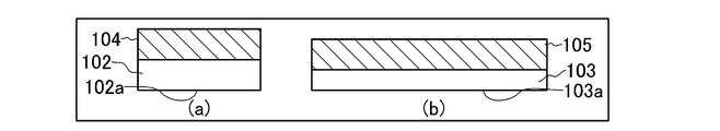
- Non-Patent Document 2 proposes a semiconductor device that attempts to improve heat dissipation of a WLP structure. This semiconductor device will be described with reference to FIG. In this semiconductor device, two semiconductor chips 302 and semiconductor chips 303 having different thicknesses are sealed on the wiring layer 301 by the mold resin layer 305.
- the heat sink 307 is arranged directly above the mold resin layer 305 and the thickest semiconductor chip 302. Further, the heat radiating plate 307 and the semiconductor chip 303 are connected via a heat transfer plate 306.
- the integrated circuit 302a of the semiconductor chip 302 and the integrated circuit 303a of the semiconductor chip 303 are electrically connected via the wiring 301a formed in the wiring layer 301. Further, a terminal 301b is arranged below the wiring layer 301, and the wiring layer 301 is connected (mounted) to the printed circuit board 308 via the terminal 301b.
- the heat generated in the semiconductor chip 302 is transferred to the heat sink 307 and diffused into the atmosphere from the heat sink 307, so that the heat dissipation of the WLP can be improved.
- Non-Patent Document 2 a semiconductor device for which an attempt is made to improve the heat dissipation of the WLP structure will be described with reference to FIG. 5 (Non-Patent Document 2).
- the semiconductor chips 312 and 313 having the same shape are sealed by the molded resin layer 305.
- the mold resin layer 305 is formed to be about 100 ⁇ m thicker than the thickness of the semiconductor chips 312 and 313, and the back surface of the semiconductor chips 312 and 313 on which the functional circuit (integrated circuit) is not formed is completely covered with the mold resin layer 305. Has been done.
- a heat sink 307 made of metal is arranged on the mold resin layer 305 via a heat conductive layer 309 made of a heat conductive material.
- the heat conductive layer 309 also functions as an adhesive layer between the mold resin layer 305 and the heat radiating plate 307.
- the heat conductive layer 309 has a thickness of about 40 ⁇ m.
- a wiring layer 301 is provided below the semiconductor chip 312, the semiconductor chip 313, and the mold resin layer 305.
- the integrated circuit 312a of the semiconductor chip 312 and the integrated circuit 313a of the semiconductor chip 313 are electrically connected via the wiring 301a formed in the wiring layer 301. Further, a terminal 301b is arranged below the wiring layer 301, and the wiring layer 301 is connected (mounted) to the printed circuit board 308 via the terminal 301b.
- a molded resin layer 305 having a relatively high thermal conductivity is used, and its value is 3.1 W / mK.
- the heat sink 307 is made of copper. According to the above structure, the heat generated in the semiconductor chip is transferred from the heat radiating plate 307 via the mold resin layer 305 and the heat conductive material while the thermal and electrical crosstalk is suppressed by the mold resin layer 305. Since it diffuses into the atmosphere, the heat dissipation of the WLP can be improved.
- a heat sink is attached to each package.
- the semiconductor chip 302 and the heat sink 307 are directly connected, and the semiconductor chip 303 and the heat sink 307 are connected via the heat transfer plate 306.
- the heat dissipation property can be improved by sealing the mold resin layer 305.
- the semiconductor chip 302 and the semiconductor chip 303 are thermally and electrically connected via the heat radiating plate 307 and the heat transfer plate 306. Therefore, for example, when a semiconductor chip 302 having a large calorific value and a semiconductor chip 303 having a small calorific value are mounted, heat is transferred from the semiconductor chip 302 having a large calorific value to the semiconductor chip 303 having a small calorific value. As a result, the temperature of the semiconductor chip 303 having a small calorific value may exceed the allowable upper limit temperature. Further, depending on the conductivity of the semiconductor chip, the potentials on the circuit surface become equal. Such thermal and electrical crosstalk can lead to unexpected defects.
- the semiconductor chip 312, the semiconductor chip 313, and the heat sink 307 are connected via the mold resin layer 305. Therefore, the mold resin layer 305 suppresses thermal and electrical crosstalk. On the other hand, since the back surfaces of the semiconductor chip 312 and the semiconductor chip 313 are sealed with the mold resin layer 305, the effect of improving heat dissipation is limited.
- Non-Patent Document 2 attempts to increase the heat dissipation efficiency from the semiconductor chip 312 and the semiconductor chip 313 to the heat radiating plate 307 by increasing the thermal conductivity of the mold resin layer 305.
- the thermal conductivity of the molded resin layer 305 is 3.1 W / mK at the highest, which is inferior to that of Si as a semiconductor material and copper used for a heat sink.
- Such a molded resin layer 305 having a low thermal conductivity also becomes a bottleneck for heat dissipation.
- the present invention has been made to solve the above problems, and an object thereof is to be able to suppress thermal and electrical crosstalk while improving heat dissipation.
- the semiconductor device includes a wiring layer on which wiring is formed, a first semiconductor chip and a second semiconductor chip arranged on the wiring layer and molded by a mold resin layer made of a mold resin, and a first semiconductor.
- a first integrated circuit formed on the main surface facing the wiring layer of the chip and connected to the wiring, and a second integrated circuit formed on the main surface facing the wiring layer of the second semiconductor chip and connected to the wiring.
- the first heat dissipation plate which is formed in contact with the back surface of the first semiconductor chip and is composed of a material having a higher thermal conductivity than the first semiconductor chip, and the heat dissipation surface is exposed to the outside from the mold resin layer, and the second semiconductor chip. It is provided with a second heat radiating plate which is formed in contact with the back surface, is made of a material having a higher thermal conductivity than the second semiconductor chip, and has a heat radiating surface exposed to the outside from the mold resin layer.
- the method for manufacturing a semiconductor device is made of a material having a thermal conductivity higher than that of the first semiconductor chip, which is in contact with the back surface of the first semiconductor chip having a first integrated circuit formed on the main surface.
- the first step of fixing the heat dissipation plate and the second heat dissipation made of a material having a higher thermal conductivity than the second semiconductor chip in contact with the back surface of the second semiconductor chip having a second integrated circuit formed on the main surface.
- a heat radiating plate whose heat radiating surface is exposed to the outside from the mold resin layer is provided in contact with the back surface of each semiconductor chip. Thermal and electrical crosstalk can be suppressed.
- FIG. 1 is a cross-sectional view showing a configuration of a semiconductor device according to an embodiment of the present invention.
- FIG. 2A is a cross-sectional view showing a state of a semiconductor device in an intermediate process for explaining a method for manufacturing a semiconductor device according to an embodiment of the present invention.
- FIG. 2B is a cross-sectional view showing a state of the semiconductor device in the intermediate process for explaining the manufacturing method of the semiconductor device according to the embodiment of the present invention.
- FIG. 2C is a cross-sectional view showing a state of the semiconductor device in the intermediate process for explaining the manufacturing method of the semiconductor device according to the embodiment of the present invention.
- FIG. 2A is a cross-sectional view showing a state of a semiconductor device in an intermediate process for explaining a method for manufacturing a semiconductor device according to an embodiment of the present invention.
- FIG. 2B is a cross-sectional view showing a state of the semiconductor device in the intermediate process for explaining the manufacturing method of the semiconductor device according to the embodiment of the present invention
- FIG. 2D is a cross-sectional view showing a state of the semiconductor device in the intermediate process for explaining the manufacturing method of the semiconductor device according to the embodiment of the present invention.
- FIG. 2E is a cross-sectional view showing a state of the semiconductor device in the intermediate process for explaining the method for manufacturing the semiconductor device according to the embodiment of the present invention.
- FIG. 2F is a cross-sectional view showing a state of the semiconductor device in the intermediate process for explaining the manufacturing method of the semiconductor device according to the embodiment of the present invention.
- FIG. 2G is a cross-sectional view showing a state of a semiconductor device in an intermediate process for explaining a method for manufacturing a semiconductor device according to an embodiment of the present invention.
- FIG. 2H is a cross-sectional view showing a state of the semiconductor device in the intermediate process for explaining the method for manufacturing the semiconductor device according to the embodiment of the present invention.
- FIG. 3 is a cross-sectional view showing the configuration of another semiconductor device according to the embodiment of the present invention.
- FIG. 4 is a cross-sectional view showing the configuration of a semiconductor device having a WLP structure.
- FIG. 5 is a cross-sectional view showing the configuration of a semiconductor device having a WLP structure.
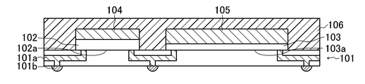
- This semiconductor device includes a wiring layer 101, and a first semiconductor chip 102 and a second semiconductor chip 103 arranged on the wiring layer 101.
- Wiring 101a made of metal is formed on the wiring layer 101.
- a first integrated circuit 102a electrically connected to the wiring 101a is formed on the main surface of the first semiconductor chip 102 facing the wiring layer 101.
- a second integrated circuit 103a electrically connected to the wiring 101a is formed on the main surface of the second semiconductor chip 103 facing the wiring layer 101.
- the first integrated circuit 102a and the second integrated circuit 103a are connected by wiring 101a.
- the first semiconductor chip 102 and the second semiconductor chip 103 are molded on the wiring layer 101 by a mold resin layer 106 made of a mold resin.
- this semiconductor device includes a first heat radiating plate 104 formed in contact with the back surface of the first semiconductor chip 102 and a second heat radiating plate 105 formed in contact with the back surface of the second semiconductor chip 103.
- the first heat radiating plate 104 is made of a material having a higher thermal conductivity than the first semiconductor chip 102, and the heat radiating surface is exposed to the outside from the mold resin layer 106.
- the second heat radiating plate 105 is made of a material having a higher thermal conductivity than the second semiconductor chip 103, and the heat radiating surface is exposed to the outside from the mold resin layer 106.
- the heat dissipation surface is the surface opposite to the side of each semiconductor chip.
- the first heat sink 104 and the second heat sink 105 can be made of, for example, an insulating material such as silicon carbide, aluminum nitride, beryllium oxide, or diamond. Further, the first heat sink 104 and the second heat sink 105 can be made of a metal such as aluminum, copper, or gold.
- the total thickness of the first semiconductor chip 102 and the first heat sink 104, the total thickness of the second semiconductor chip 103 and the second heat sink 105, and the thickness of the mold resin layer 106 are Each is equal.
- the heat radiating surface of the first heat radiating plate 104 and the heat radiating surface of the second heat radiating plate 105 are exposed to the outside from the mold resin layer 106.
- the thickness of the first semiconductor chip 102 and the second semiconductor chip 103 are different from each other, but the first semiconductor chip 102 and the second semiconductor chip 103 are the same. It can also be a thickness. Further, the material of the first semiconductor chip 102 may be different from the material of the second semiconductor chip 103. Further, the thicknesses of the first heat sink 104 and the second heat sink 105 can be appropriately set.
- a terminal 101b is formed under the wiring layer 101, and the wiring layer 101 is electrically connected (mounted) to the printed circuit board 107 via the terminal 101b.
- the face-down method of WLP and the secondary mounting on the printed circuit board 107 are exemplified, but it is also possible to use another method such as the face-up method of WLP or a design in which the secondary mounting is not performed. The effect of the present invention can be obtained.
- the first semiconductor chip 102 and the second semiconductor chip 103 are thermally and electrically formed by the mold resin layer 106 in the plane direction of the wiring layer 101. It is separated. Further, the first heat sink 104 connected to the first semiconductor chip 102 and the second heat sink 105 connected to the second semiconductor chip 103 are thermally and electrically separated by the mold resin layer 106. Therefore, the first semiconductor chip 102 and the second semiconductor chip 103 are thermally separated. Further, regardless of the conductivity of the main body of each semiconductor chip, the potentials of the surfaces on which the integrated circuits are formed are not equal.
- the heat of the first semiconductor chip 102 is radiated from the heat radiating surface that can come into contact with the outside air via the first heat radiating plate 104 that is directly connected to the first semiconductor chip 102.
- the heat of the second semiconductor chip 103 is dissipated from the heat radiating surface that can come into contact with the outside air via the second heat radiating plate 105 that is directly connected to the second semiconductor chip 103.
- the heat dissipation property due to the sealing of the mold resin layer 106 is improved.
- thermal and electrical crosstalk can be suppressed while improving heat dissipation.
- the thermal conductivity is higher than that of the first semiconductor chip 102 in contact with the back surface of the first semiconductor chip 102 in which the first integrated circuit 102a is formed on the main surface.
- the first heat sink 104 made of a material is fixed (first step).
- the thermal conductivity is higher than that of the second semiconductor chip 103 in contact with the back surface of the second semiconductor chip 103 in which the second integrated circuit 103a is formed on the main surface.
- a second heat sink 105 made of a material is fixed (second step).
- the first heat-dissipating wafer to be the first heat-dissipating plate 104 is bonded to the first wafer forming the first semiconductor chip 102, and the second heat-dissipating plate 105 is formed to the second wafer forming the second semiconductor chip 103.
- the above-mentioned process can be carried out.
- a known semiconductor wafer bonding technique for example, surface activated bonding
- the first wafer and the second wafer are thinly layered so that the thicknesses of the first wafer to which the first heat dissipation wafer is bonded and the second wafer to which the second heat radiation wafer is bonded are equal to each other. Wafer and polish.
- a semiconductor layer is formed on the first wafer and the second wafer by a known crystal growth technique, and a desired functional circuit is formed on these semiconductor layers by carrying out a known semiconductor process.
- a plurality of first integrated circuits 102a are formed on the first wafer, and a plurality of second integrated circuits 103a are formed on the second wafer (FIG. 2B).
- the first heat sink 104 is formed on the back surface of the first semiconductor chip 102 in which the first integrated circuit 102a is formed on the main surface. It shall be in a fixed state.
- the second heat sink 105 is fixed to the back surface of the second semiconductor chip 103 in which the second integrated circuit 103a is formed on the main surface.
- the forming surface of the first integrated circuit 102a of the first semiconductor chip 102 cut out on the chip is attached and fixed to the adhesive layer 122 fixed on the support substrate 121. Further, the forming surface of the second integrated circuit 103a of the second semiconductor chip 103 cut out on the chip is attached and fixed to the adhesive layer 122 (third step, fourth step).
- the figure shows one set of the first semiconductor chip 102 and the second semiconductor chip 103, for example, a plurality of sets can be fixed (mounted) on the support substrate 121 at the same time.
- the support substrate 121 may have a size corresponding to the semiconductor manufacturing apparatus used when forming the wiring layer 101 described later.
- the material of the support substrate 121 can be made of, for example, a semiconductor such as silicon, glass, a resin, a metal, or the like.
- the adhesive layer 122 can be made of a material that can withstand the temperature in the formation of the mold resin layer 106, which will be described later.
- the first semiconductor chip 102 to which the first heat sink 104 is fixed and the second semiconductor chip 103 to which the second heat sink 105 is fixed are molded with a mold resin. Molding is performed to form the mold resin layer 106 (fifth step).
- the mold resin layer 106 can be formed by forming a mold resin layer by, for example, a known compression molding method or a transfer molding method, and curing the formed mold resin layer.
- the mold resin layer 106 is separated from the support substrate 121 (sixth step), and the integrated circuit forming surface is exposed as shown in FIG. 2F.
- the mold resin layer 106 can be separated from the support substrate 121 by peeling off the adhesive layer 122.
- a method that does not deteriorate the characteristics of each integrated circuit such as a laser peeling method, a thermal peeling method, a mechanical peeling method, and a solvent peeling method, can be selected.
- the first semiconductor chip 102 and the second semiconductor chip 103 are formed on the wiring layer 101 provided with the wiring 101a. ..
- the first integrated circuit 102a and the second integrated circuit 103a are connected to the wiring 101a. Further, on the wiring layer 101, the first semiconductor chip 102 and the second semiconductor chip 103 are in a state of being molded by the mold resin layer 106 (7th step).
- the wiring layer 101 can be formed on the first semiconductor chip 102 and the second semiconductor chip 103 molded by the mold resin layer 106 by the build-up method.
- a metal layer is formed on the mold resin layer 106 by, for example, thin-film deposition or a plating method, and the metal layer is patterned.
- the wiring 101a can be formed into the wiring layer 101.
- the terminal 101b connected to the wiring 101a is formed on the wiring layer 101 by, for example, a solder bump.
- the figure shows one set of the first semiconductor chip 102 and the second semiconductor chip 103, for example, a plurality of sets can be simultaneously molded with the mold resin layer 106.
- the heat radiating surface of the first heat radiating plate 104 and the radiating surface of the second heat radiating plate 105 are exposed to the outside from the mold resin layer 106 (step 8).
- the surface of the wiring layer 101 on the side where the heat sink is arranged is mechanically polished (ground and polished) with a grinder or the like to expose the heat dissipation surface of the first heat sink 104 and the heat dissipation surface of the second heat sink 105.
- a dicing device each set of the first semiconductor chip 102 and the second semiconductor chip 103 is separated into individual pieces.
- the semiconductor device is mounted on the printed circuit board 107 via the terminal 101b of the package composed of the set of the first semiconductor chip 102 and the second semiconductor chip 103, which are separated into individual pieces, to obtain the semiconductor device shown in FIG.
- the semiconductor device can be mounted by a known reflow technique.
- the first semiconductor chip 102 and the second semiconductor chip 103 are separated by the mold resin layer 106, the first heat radiating plate 104 and the second heat radiating plate 105 Thermal and electrical crosstalk between are suppressed.
- the heat generated from the first integrated circuit 102a and the second integrated circuit 103a of the first semiconductor chip 102 and the second semiconductor chip 103 is from the chip main body of the semiconductor chip to the first heat sink 104 and the second heat sink 104 having high thermal conductivity. It is transmitted to the heat sink 105 and then diffused into the atmosphere.
- the mold resin layer 106 having a remarkably low thermal conductivity does not intervene in the heat dissipation path, the heat dissipation can be improved.
- the thermal conductivity is not caused to cause element destruction due to insufficient mechanical strength during the manufacturing process.
- the semiconductor portion of the semiconductor chip having a low heat sink can be made extremely thin, and the heat dissipation efficiency can be improved.
- dicing can be performed after bonding a heat sink of the same size to the semiconductor wafer. Therefore, since the semiconductor chip provided with the heat sink in advance can be converted into WLP, the mounting process can be shortened in time without attaching the heat sink for each package.
- the advantage of the WLP manufacturing method is that it can be manufactured in a batch at the wafer level, but conventionally, when mounting a heat sink, it is necessary to mount it for each package, and the heat sink mounting process leads to an increase in time in the mounting process. Was there.
- it is possible to suppress thermal / electrical crosstalk and shorten the time required for the mounting process while improving heat dissipation.
- the mold resin and each semiconductor chip are scraped.
- the physical property values of the mold resin and each semiconductor chip it is necessary to consider the physical property values of the mold resin and each semiconductor chip as the grinding conditions.
- the molding resin and two types of semiconductor chips made of different materials must be subjected to grinding conditions for each combination of semiconductor chips.
- the search condition is a combination of the mold resin and the heat sink of a specific type, the grinding condition does not depend on the semiconductor chip, and there is an advantage that the grinding condition can be easily set. doing.
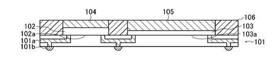
- FIG. 3 it is also possible to have a configuration having an uneven structure formed on each of the heat radiating surface of the first heat radiating plate 104a and the heat radiating surface of the second heat radiating plate 105a.
- a concavo-convex structure can be formed on each of the heat-dissipating surface of the first heat-dissipating plate 104a and the heat-dissipating surface of the second heat-dissipating plate 105a.
- a heat radiating plate whose heat radiating surface is exposed to the outside from the mold resin layer is provided in contact with the back surface of each semiconductor chip, so that the heat radiating property can be improved. , It becomes possible to suppress thermal and electrical crosstalk.
Landscapes
- Cooling Or The Like Of Semiconductors Or Solid State Devices (AREA)
- Physics & Mathematics (AREA)
- Geometry (AREA)
Priority Applications (3)
| Application Number | Priority Date | Filing Date | Title |
|---|---|---|---|
| US17/922,944 US20230154822A1 (en) | 2020-05-20 | 2020-05-20 | Semiconductor Device and Method for Manufacturing The Same |
| PCT/JP2020/019912 WO2021234849A1 (ja) | 2020-05-20 | 2020-05-20 | 半導体装置およびその製造方法 |
| JP2022524751A JPWO2021234849A1 (https=) | 2020-05-20 | 2020-05-20 |
Applications Claiming Priority (1)
| Application Number | Priority Date | Filing Date | Title |
|---|---|---|---|
| PCT/JP2020/019912 WO2021234849A1 (ja) | 2020-05-20 | 2020-05-20 | 半導体装置およびその製造方法 |
Publications (1)
| Publication Number | Publication Date |
|---|---|
| WO2021234849A1 true WO2021234849A1 (ja) | 2021-11-25 |
Family
ID=78708278
Family Applications (1)
| Application Number | Title | Priority Date | Filing Date |
|---|---|---|---|
| PCT/JP2020/019912 Ceased WO2021234849A1 (ja) | 2020-05-20 | 2020-05-20 | 半導体装置およびその製造方法 |
Country Status (3)
| Country | Link |
|---|---|
| US (1) | US20230154822A1 (https=) |
| JP (1) | JPWO2021234849A1 (https=) |
| WO (1) | WO2021234849A1 (https=) |
Cited By (2)
| Publication number | Priority date | Publication date | Assignee | Title |
|---|---|---|---|---|
| US20230154816A1 (en) * | 2021-11-17 | 2023-05-18 | Adeia Semiconductor Bonding Technologies Inc. | Thermal bypass for stacked dies |
| US12543568B2 (en) | 2021-12-20 | 2026-02-03 | Adeia Semiconductor Bonding Technologies Inc. | Thermoelectric cooling for die packages |
Citations (2)
| Publication number | Priority date | Publication date | Assignee | Title |
|---|---|---|---|---|
| JPH098209A (ja) * | 1995-06-15 | 1997-01-10 | Hitachi Ltd | 半導体装置およびモールド金型 |
| WO2018181236A1 (ja) * | 2017-03-31 | 2018-10-04 | パナソニックIpマネジメント株式会社 | 半導体装置及びその製造方法 |
Family Cites Families (3)
| Publication number | Priority date | Publication date | Assignee | Title |
|---|---|---|---|---|
| US5430331A (en) * | 1993-06-23 | 1995-07-04 | Vlsi Technology, Inc. | Plastic encapsulated integrated circuit package having an embedded thermal dissipator |
| US8237252B2 (en) * | 2009-07-22 | 2012-08-07 | Stats Chippac, Ltd. | Semiconductor device and method of embedding thermally conductive layer in interconnect structure for heat dissipation |
| US8987876B2 (en) * | 2013-03-14 | 2015-03-24 | General Electric Company | Power overlay structure and method of making same |
-
2020
- 2020-05-20 JP JP2022524751A patent/JPWO2021234849A1/ja active Pending
- 2020-05-20 WO PCT/JP2020/019912 patent/WO2021234849A1/ja not_active Ceased
- 2020-05-20 US US17/922,944 patent/US20230154822A1/en not_active Abandoned
Patent Citations (2)
| Publication number | Priority date | Publication date | Assignee | Title |
|---|---|---|---|---|
| JPH098209A (ja) * | 1995-06-15 | 1997-01-10 | Hitachi Ltd | 半導体装置およびモールド金型 |
| WO2018181236A1 (ja) * | 2017-03-31 | 2018-10-04 | パナソニックIpマネジメント株式会社 | 半導体装置及びその製造方法 |
Cited By (2)
| Publication number | Priority date | Publication date | Assignee | Title |
|---|---|---|---|---|
| US20230154816A1 (en) * | 2021-11-17 | 2023-05-18 | Adeia Semiconductor Bonding Technologies Inc. | Thermal bypass for stacked dies |
| US12543568B2 (en) | 2021-12-20 | 2026-02-03 | Adeia Semiconductor Bonding Technologies Inc. | Thermoelectric cooling for die packages |
Also Published As
| Publication number | Publication date |
|---|---|
| JPWO2021234849A1 (https=) | 2021-11-25 |
| US20230154822A1 (en) | 2023-05-18 |
Similar Documents
| Publication | Publication Date | Title |
|---|---|---|
| CN110957229B (zh) | 半导体器件和形成半导体器件的方法 | |
| JP5635247B2 (ja) | マルチチップモジュール | |
| TWI649845B (zh) | 半導體封裝結構及其製造方法 | |
| US20240371776A1 (en) | Manufacturing method of semiconductor package | |
| CN103329266B (zh) | 具有连接有源芯片的插板的堆叠微电子组件 | |
| US5273940A (en) | Multiple chip package with thinned semiconductor chips | |
| TW202008479A (zh) | 晶片封裝體結構之製造方法 | |
| CN101211945A (zh) | 具晶粒接收通孔的半导体影像元件封装结构及其方法 | |
| TWI409923B (zh) | 具有晶粒埋入式以及雙面覆蓋重增層之基板結構及其方法 | |
| KR20080089311A (ko) | Wlp용 다이 수용 스루홀 및 양 표면 위에 이중 사이드빌드업층들을 갖는 반도체 디바이스 패키지 및 그 방법 | |
| CN101202253A (zh) | 具有良好热膨胀系数效能的圆片级封装及其方法 | |
| KR20080082545A (ko) | 반도체 디바이스 패키지 구조 및 그 방법 | |
| JP6971052B2 (ja) | 半導体装置の製造方法および半導体装置 | |
| US20250316616A1 (en) | Semiconductor package and manufacturing method thereof | |
| US9799626B2 (en) | Semiconductor packages and other circuit modules with porous and non-porous stabilizing layers | |
| WO2023241304A1 (zh) | 芯片封装方法及芯片 | |
| CN114005812A (zh) | 一种扇出型封装结构及其构造方法 | |
| KR100660604B1 (ko) | 금속 박편을 이용한 수동 소자 및 반도체 패키지의제조방법 | |
| TWI898406B (zh) | 半導體封裝方法及半導體封裝結構 | |
| US20120211895A1 (en) | Chip module and method for providing a chip module | |
| WO2021234849A1 (ja) | 半導体装置およびその製造方法 | |
| US7906833B2 (en) | Semiconductor device and manufacturing method thereof | |
| US20080029865A1 (en) | Electronic Device and Method For Producing the Same | |
| JP7697524B2 (ja) | 半導体装置およびその製造方法 | |
| JP3651362B2 (ja) | 半導体装置の製造方法 |
Legal Events
| Date | Code | Title | Description |
|---|---|---|---|
| 121 | Ep: the epo has been informed by wipo that ep was designated in this application |
Ref document number: 20936855 Country of ref document: EP Kind code of ref document: A1 |
|
| ENP | Entry into the national phase |
Ref document number: 2022524751 Country of ref document: JP Kind code of ref document: A |
|
| NENP | Non-entry into the national phase |
Ref country code: DE |
|
| 122 | Ep: pct application non-entry in european phase |
Ref document number: 20936855 Country of ref document: EP Kind code of ref document: A1 |