WO2021230224A1 - 伝送線路 - Google Patents
伝送線路 Download PDFInfo
- Publication number
- WO2021230224A1 WO2021230224A1 PCT/JP2021/017809 JP2021017809W WO2021230224A1 WO 2021230224 A1 WO2021230224 A1 WO 2021230224A1 JP 2021017809 W JP2021017809 W JP 2021017809W WO 2021230224 A1 WO2021230224 A1 WO 2021230224A1
- Authority
- WO
- WIPO (PCT)
- Prior art keywords
- conductor
- connection
- connection electrode
- electrode
- ground conductor
- Prior art date
- Legal status (The legal status is an assumption and is not a legal conclusion. Google has not performed a legal analysis and makes no representation as to the accuracy of the status listed.)
- Ceased
Links
Images


Classifications
-
- H—ELECTRICITY
- H01—ELECTRIC ELEMENTS
- H01P—WAVEGUIDES; RESONATORS, LINES, OR OTHER DEVICES OF THE WAVEGUIDE TYPE
- H01P3/00—Waveguides; Transmission lines of the waveguide type
- H01P3/02—Waveguides; Transmission lines of the waveguide type with two longitudinal conductors
- H01P3/08—Microstrips; Strip lines
-
- H—ELECTRICITY
- H05—ELECTRIC TECHNIQUES NOT OTHERWISE PROVIDED FOR
- H05K—PRINTED CIRCUITS; CASINGS OR CONSTRUCTIONAL DETAILS OF ELECTRIC APPARATUS; MANUFACTURE OF ASSEMBLAGES OF ELECTRICAL COMPONENTS
- H05K1/00—Printed circuits
- H05K1/02—Details
- H05K1/0296—Conductive pattern lay-out details not covered by sub groups H05K1/02 - H05K1/0295
-
- H—ELECTRICITY
- H01—ELECTRIC ELEMENTS
- H01P—WAVEGUIDES; RESONATORS, LINES, OR OTHER DEVICES OF THE WAVEGUIDE TYPE
- H01P3/00—Waveguides; Transmission lines of the waveguide type
- H01P3/02—Waveguides; Transmission lines of the waveguide type with two longitudinal conductors
- H01P3/026—Coplanar striplines [CPS]
-
- H—ELECTRICITY
- H01—ELECTRIC ELEMENTS
- H01Q—ANTENNAS, i.e. RADIO AERIALS
- H01Q1/00—Details of, or arrangements associated with, antennas
- H01Q1/48—Earthing means; Earth screens; Counterpoises
-
- H—ELECTRICITY
- H05—ELECTRIC TECHNIQUES NOT OTHERWISE PROVIDED FOR
- H05K—PRINTED CIRCUITS; CASINGS OR CONSTRUCTIONAL DETAILS OF ELECTRIC APPARATUS; MANUFACTURE OF ASSEMBLAGES OF ELECTRICAL COMPONENTS
- H05K1/00—Printed circuits
- H05K1/02—Details
- H05K1/0213—Electrical arrangements not otherwise provided for
- H05K1/0216—Reduction of cross-talk, noise or electromagnetic interference
-
- H—ELECTRICITY
- H01—ELECTRIC ELEMENTS
- H01P—WAVEGUIDES; RESONATORS, LINES, OR OTHER DEVICES OF THE WAVEGUIDE TYPE
- H01P3/00—Waveguides; Transmission lines of the waveguide type
-
- H—ELECTRICITY
- H05—ELECTRIC TECHNIQUES NOT OTHERWISE PROVIDED FOR
- H05K—PRINTED CIRCUITS; CASINGS OR CONSTRUCTIONAL DETAILS OF ELECTRIC APPARATUS; MANUFACTURE OF ASSEMBLAGES OF ELECTRICAL COMPONENTS
- H05K1/00—Printed circuits
- H05K1/02—Details
- H05K1/0277—Bendability or stretchability details
- H05K1/028—Bending or folding regions of flexible printed circuits
-
- H—ELECTRICITY
- H05—ELECTRIC TECHNIQUES NOT OTHERWISE PROVIDED FOR
- H05K—PRINTED CIRCUITS; CASINGS OR CONSTRUCTIONAL DETAILS OF ELECTRIC APPARATUS; MANUFACTURE OF ASSEMBLAGES OF ELECTRICAL COMPONENTS
- H05K2201/00—Indexing scheme relating to printed circuits covered by H05K1/00
- H05K2201/09—Shape and layout
- H05K2201/09209—Shape and layout details of conductors
- H05K2201/09218—Conductive traces
- H05K2201/09281—Layout details of a single conductor
Definitions
- the present invention relates to a transmission line configured on a substrate.
- This signal transmission line comprises a laminated insulator, a signal conductor pattern, and two ground conductor patterns.
- the laminated insulator is composed of a plurality of laminated insulator layers.
- the signal conductor pattern and the ground conductor pattern are formed on the laminated insulator.
- the signal conductor pattern is placed between the ground conductor patterns.
- the interlayer connection conductors are arranged in series below the mounting electrode on which the electronic component is mounted, the flatness of the mounting electrode may be impaired.
- the mounting electrodes it is preferable that the mounting electrodes have high flatness. However, if a conductor pattern is used to maintain the flatness of the mounting electrode, the characteristic impedance may shift this time.
- An object of the present invention is to provide a transmission line that can maintain the flatness of the mounting electrode and suppress the deviation of the characteristic impedance.
- the transmission line of the present invention is formed on a substrate having a plurality of insulator layers, a mounting electrode formed on the surface layer of the substrate, a signal conductor formed in the substrate, and the plurality of insulations formed on the substrate.
- the first ground conductor that overlaps the signal conductor when viewed from the stacking direction of the body layer, the mounting electrode, and the signal conductor are electrically connected and arranged between the signal conductor and the first ground conductor in the stacking direction.
- a first interlayer connection conductor electrically connected between the mounting electrode and the first connection electrode and joined to the first connection electrode, a signal conductor, and the first connection.
- the first ground conductor comprises a second interlayer connecting conductor that is electrically connected between the electrodes, is bonded to the first connecting electrode, and does not overlap the first interlayer connecting conductor when viewed from the stacking direction. When viewed from the stacking direction, it does not overlap with at least a part of the first connecting electrode.
- the flatness of the mounted electrode can be maintained and the deviation of the characteristic impedance of the transmission line can be suppressed.
- FIG. 1 is a plan view of a transmission line 10 according to the first embodiment of the present invention.
- FIG. 2 is a cross-sectional view taken along the line AA of the transmission line 10.
- FIG. 3 is a plan view of a main part of the transmission line 10.
- FIG. 4 is a plan view of the first connection electrode 171 according to the first embodiment.
- 5 (A), FIG. 5 (B), FIG. 5 (C), FIG. 5 (D), and FIG. 5 (E) are plan views of the first connection electrode 171 according to the modified example of the first embodiment.
- FIG. 6 is a plan view of a main part of the transmission line 30 according to still another modification of the first embodiment.
- FIG. 1 is a plan view of a transmission line 10 according to the first embodiment of the present invention.
- FIG. 2 is a cross-sectional view taken along the line AA of the transmission line 10.
- FIG. 3 is a plan view of a main part of the transmission line 10.
- FIG. 4 is a plan view of the
- FIG. 7 is a plan view of a main part of the transmission line 40 according to still another modification of the first embodiment.
- FIG. 8 is a plan view of the mounting electrode 42, the signal conductor 43, and the first connection electrode 471.
- FIG. 9 is a cross-sectional view of the transmission line 70 according to the second embodiment of the present invention.
- FIG. 10 is a plan view of a main part of the transmission line 70.
- FIG. 11 is a plan view of the first connection electrode 771.
- 12 (A) and 12 (B) are plan views of the first connection electrode 871,971 according to the modified example of the second embodiment. It is sectional drawing of the transmission line which concerns on other embodiment. It is sectional drawing of the transmission line which concerns on other embodiment. It is sectional drawing of the transmission line which concerns on other embodiment. It is sectional drawing of the transmission line which concerns on other embodiment. It is sectional drawing of the transmission line which concerns on other embodiment. It is sectional drawing of the transmission line which concerns on other embodiment. It is sectional drawing
- FIG. 1 is a plan view of a transmission line 10 according to the first embodiment of the present invention.
- FIG. 2 is a cross-sectional view taken along the line AA of the transmission line 10.
- FIG. 3 is a plan view of a main part of the transmission line 10. In FIG. 3, the resist film 191 is not shown.
- the transmission line 10 has a planar shape and extends in one direction.
- the transmission line 10 includes a substrate 11, a mounting electrode 12, a signal conductor 13, ground conductors 141, 142, an interlayer connection conductor 16, and a connection electrode 17.
- the connection electrode 17 includes a first connection electrode 171 and a second connection electrode 172 and 173.
- the interlayer connecting conductor 16 includes a first interlayer connecting conductor 161 and a second interlayer connecting conductor 162, and an interlayer connecting conductor 163, 164, and 165.
- the ground conductor 141 is an example of the "first ground conductor" of the present invention.
- the ground conductor 142 is an example of the "second ground conductor” of the present invention.
- the electronic component 20 is mounted on the first main surface S1 of the substrate 11.
- the electronic component 20 has an aligned connection terminal (signal terminal) 21 and a connection terminal (ground terminal) 22.
- the transmission line 10 includes a connecting portion 151 connecting the mounting electrode 12 and the signal conductor 13, and a connecting portion 152 connecting the ground conductor 141 and the ground conductor 142.
- the connecting portion 151 has a first interlayer connecting conductor 161 and a second interlayer connecting conductor 162, and a first connecting electrode 171.
- the connecting portion 152 has an interlayer connecting conductor 163, 164, 165 and a second connecting electrode 172, 173.
- the transmission line 10 has a first region Z1 provided with a connection portion 151 and a second region Z2 provided with a signal conductor 13.
- the substrate 11 is composed of a plurality of laminated insulator layers 111, 112, 113, 114.
- the mounting electrode 12 is formed on the surface layer of the substrate 11.
- the signal conductor 13 is formed in the substrate 11.
- the ground conductor 141 is formed on the substrate 11 and overlaps the signal conductor 13 (in a plan view) when viewed from the stacking direction (hereinafter, simply referred to as the stacking direction) of the plurality of insulator layers 111 to 114.
- the ground conductor 142 is formed on the substrate 11 and overlaps the mounting electrode 12, the signal conductor 13, and the first connection electrode 171 in a plan view.
- the signal conductor 13, the first connection electrode 171 and the second connection electrode 172, 173 are arranged between the ground conductor 141 and the ground conductor 142 in the stacking direction.
- the signal conductor 13 is defined for each signal line.
- the signal conductor 13 is a continuous (non-separable) conductor pattern in the same layer, and has the largest area among the conductor patterns constituting the signal line and transmitting the signal.
- the first connection electrode 171 electrically connects the mounting electrode 12 and the signal conductor 13, and is arranged between the signal conductor 13 and the ground conductor 141 in the stacking direction.
- the distance between the first connection electrode 171 and the ground conductor 142 in the stacking direction is greater than or equal to the distance between the first connection electrode 171 and the ground conductor 141 in the stacking direction.
- the first interlayer connection conductor 161 is electrically connected between the mounting electrode 12 and the first connection electrode 171 and is joined to the first connection electrode 171.
- the second interlayer connection conductor 162 is electrically connected between the signal conductor 13 and the first connection electrode 171 and is joined to the first connection electrode 171.
- the second interlayer connecting conductor 162 does not overlap with the first interlayer connecting conductor 161 in a plan view.
- the first interlayer connecting conductor 161 and the second interlayer connecting conductor 162 are not aligned linearly in the stacking direction.
- the ground conductor 141 does not overlap the first connection electrode 171 in a plan view.
- the second connection electrodes 172 and 173 electrically connect the ground conductor 141 and the ground conductor 142.
- the first connection electrode 171 and the second connection electrodes 172 and 173 do not overlap in a plan view.
- the interlayer connecting conductors 163 to 165 constituting the connecting portion 152 are the first interlayer connecting conductors 161 constituting the connecting portion 151. And does not overlap the second interlayer connection conductor 162.
- the insulator layers 111 to 114 are arranged in this order from the upper side to the lower side.
- the insulator layers 111 to 114 are made of a thermoplastic resin such as a liquid crystal polymer (LCP), but may be made of another insulating material.
- the insulator layers 111 to 114 are integrated by, for example, a heat press, but may be bonded to each other with an adhesive.
- the terms “upper side” and “lower side” are for convenience to distinguish one side from the other side.
- the terms “upper surface” and “lower surface” are for convenience to distinguish between the main surface on one side and the main surface on the other side.
- the mounting electrode 12 and the ground conductor 141 are arranged on the first main surface S1 of the substrate 11, that is, on the upper surface of the insulator layer 111.
- the first connection electrode 171 and the second connection electrode 172 are arranged on the upper surface of the insulator layer 112.
- the signal conductor 13 and the second connection electrode 173 are arranged on the upper surface of the insulator layer 113.
- the ground conductor 142 is arranged on the second main surface S2 on the substrate 11 opposite to the first main surface S1, that is, on the lower surface of the insulator layer 114.
- the mounting electrode 12, the signal conductor 13, the ground conductor 141, 142, and the connecting electrode 17 are conductor patterns, and are formed by, for example, patterning a Cu foil.
- the first interlayer connection conductor 161 and the interlayer connection conductor 163 are arranged on the insulator layer 111.
- the second interlayer connecting conductor 162 and the interlayer connecting conductor 164 are arranged on the insulator layer 112.
- the interlayer connection conductor 165 is arranged on the insulator layers 113 and 114.
- the interlayer connection conductor 16 is formed, for example, by curing the electric paste filled in the through holes of the insulator layers 111 to 114.
- the signal conductor 13 is stretched in the same direction as the stretching direction of the transmission line 10, and is arranged between the ground conductors 141 and 142 facing each other. This forms a stripline structure.
- the ground conductor 141 has a slit SL1.
- the slit SL1 has a rectangular shape, but may have another shape.
- the mounting electrode 12 and the first connecting electrode 171 are arranged in the slit SL1 in a plan view.
- the slit SL1 is preferably formed along the stretching direction of the first connection electrode 171 in order to improve the signal characteristics.
- ground conductor 141 is individually provided with a plurality of slits SL1, some or all of the slits SL1 may be connected to each other.
- FIG. 4 is a plan view of the first connection electrode 171 according to the first embodiment.
- the shape of the first connection electrode 171 is depicted more specifically than in FIG.
- the positions of the first interlayer connecting conductor 161 and the second interlayer connecting conductor 162, the direction ⁇ of the straight line connecting the positions of the first interlayer connecting conductor 161 and the position of the second interlayer connecting conductor 162, and the direction ⁇ are perpendicular to the direction ⁇ .
- Direction ⁇ is also shown.
- the first connecting electrode 171 has a portion joined to the first interlayer connecting conductor 161, a portion joined to the second interlayer connecting conductor 162, and a portion extending between them.
- the width of the first connecting electrode is the length of the first connecting electrode in the direction perpendicular to the direction of the straight line connecting the position of the first interlayer connecting conductor and the position of the second interlayer connecting conductor in a plan view.
- the width of the signal conductor is the length of the signal conductor in the direction perpendicular to the extending direction of the signal conductor in a plan view.
- the width of the mounting electrode is the length of the mounting electrode in a direction perpendicular to the direction of the straight line connecting the position of the interlayer connecting conductor joined to the mounting electrode and the position of the connecting terminal joined to the mounting electrode in a plan view. ..
- FIG. 5 (A), FIG. 5 (B), FIG. 5 (C), FIG. 5 (D), and FIG. 5 (E) are plan views of the first connection electrode 171 according to the modified example of the first embodiment.
- Is. 5 (A) to 5 (E) show a straight line connecting the positions of the first interlayer connection conductor 161 and the second interlayer connection conductor 162, the position of the first interlayer connection conductor 161 and the position of the second interlayer connection conductor 162.
- the direction ⁇ and the direction ⁇ perpendicular to the direction ⁇ are also shown.
- the first connection electrode 171 may have a larger width at the central portion in the direction ⁇ .
- FIG. 5 (A) the first connection electrode 171 may have a larger width at the central portion in the direction ⁇ .
- the first interlayer connection conductor 161 or the second interlayer connection conductor 162 may protrude from the first connection electrode 171 in a plan view.
- the first connection electrode 171 may be confined at the central portion in the direction ⁇ .
- the first connecting electrode 171 may have a protrusion that is not joined to either the first interlayer connecting conductor 161 or the second interlayer connecting conductor 162.
- the first connection electrode 171 may be bent in the middle of the stretching direction.
- connection portion 151 when the substrate 11 has three or more insulator layers between the mounting electrode 12 and the signal conductor 13 will be described.
- the connection portion 151 may be composed of one first connection electrode and two or more interlayer connection conductors.
- the connection portion 151 may be composed of a plurality of first connection electrodes and three or more interlayer connection conductors. In this case, some interlayer connecting conductors of the connecting portion 151 may overlap each other in a plan view.
- the connecting portion 151 may have an interlayer connecting conductor over a plurality of insulator layers, or may have a plurality of interlayer connecting conductors arranged linearly in the stacking direction.
- the connecting portion 151 has one first connecting electrode, one interlayer connecting conductor over one layer, and one over two layers. It may be composed of two interlayer connecting conductors. Alternatively, the connecting portion 151 may be composed of one first connecting electrode, two interlayer connecting conductors aligned linearly with each other, and one interlayer connecting conductor not linearly aligned with the two interlayer connecting conductors. Alternatively, the connecting portion 151 may be composed of two first connecting electrodes and three interlayer connecting conductors.
- the connecting portion 151 may have at least one first connecting electrode. That is, the first interlayer connecting conductor and the second interlayer connecting conductor need not overlap in the stacking direction. As a result, as will be described later, the flatness of the mounting electrode 12 is improved.
- the interlayer connection conductor directly under the mounting electrode 12 physically connected to the mounting electrode 12 has a great influence on the flatness of the mounting electrode 12.
- the interlayer connection conductor connected to the interlayer connection conductor directly under the mounting electrode 12 via one first connection electrode may greatly affect the flatness of the mounting electrode 12. Therefore, it is preferable that these interlayer connection conductors do not overlap with any other interlayer connection conductors in the substrate 11. Further, it is preferable that these interlayer connection conductors are not formed over a plurality of insulator layers, and it is preferable that they do not line up linearly with other interlayer connection conductors in the stacking direction.
- the connecting portion 151 When the connecting portion 151 is composed of a plurality of connecting electrodes and three or more interlayer connecting conductors, the connecting portion 151 may have a staircase shape, a zigzag shape, or another shape.
- connection portion 152 has a zigzag shape, but may have a staircase shape or another shape.
- connection portions 151 and 152 are arranged at intervals in the width direction of the transmission line 10 corresponding to the arrangement of the connection terminals 21 and 22 of the electronic component 20.
- the connecting portion 152 is arranged so as to be closer to the electronic component 20 than the connecting portion 151 or to overlap the electronic component 20 in a plan view.
- a resist film 191 is formed on the first main surface S1 of the substrate 11.
- a resist film 192 is formed on the second main surface S2 of the substrate 11.
- the resist films 191, 192 are formed so as to cover the conductor pattern formed on the surface of the substrate 11.
- the resist film 191 is formed with an opening for exposing a part of the mounting electrode 12 and an opening for exposing a part of the ground conductor 141.
- the electronic component 20 is arranged so that its connection terminals 21 and 22 are aligned in the width direction of the transmission line 10.
- the connection terminal 21 is connected to the mounting electrode 12 exposed from the opening of the resist film 191 via the solder 231.
- the connection terminal 22 is connected to the ground conductor 141 exposed from the opening of the resist film 191 via solder.
- the electronic component 20 is an electronic component having a signal terminal such as a connector or an IC, for example.
- the design parameters of the transmission line are appropriately determined so that the desired characteristics can be obtained. Specific examples of transmission line design parameters are shown below.
- Insulator layer thickness T1 50 ⁇ m
- Conductor pattern thickness T2 12 ⁇ m
- Minimum width W1 of the first connection electrode and minimum width W3 of the signal conductor 60 ⁇ m or more and 100 ⁇ m or less
- Distance between the mounting electrode and the ground conductor D1 40 ⁇ m or more
- the minimum width W1 of the connection electrode Is defined as W3-20 ⁇ m or more and W3-10 ⁇ m or less.
- the conductor pattern is actually embedded in the insulator layer of about 1 to 2 ⁇ m.
- the first connection electrode 171 is closer to the ground conductor 141 than the signal conductor 13 in the stacking direction, but does not overlap the ground conductor 141 in a plan view. Therefore, it is suppressed that the capacitance value between the first connection electrode 171 and the ground conductor 141 is larger than the capacitance value between the signal conductor 13 and the ground conductor 141. Therefore, it is suppressed that the characteristic impedance in the first region Z1 of the transmission line 10 deviates from the characteristic impedance in the second region Z2 of the transmission line 10.
- the surface of the substrate 11 may protrude at the place where the interlayer connecting conductor 16 is formed.
- the first interlayer connection conductor 161 and the second interlayer connection conductor 162 are not linearly arranged, the deterioration of the flatness of the mounting electrode 12 is suppressed. As a result, a good connection between the mounting electrode 12 and the electronic component 20 can be obtained.
- connection portion 152 when viewed from a direction orthogonal to the stretching direction of the first connection electrode 171 and orthogonal to the stacking direction (width direction of the transmission line 10), the interlayer connection conductors 163 to 165 constituting the connection portion 152 form the connection portion 151. It does not overlap with the constituent first interlayer connection conductor 161 and the second interlayer connection conductor 162.
- connection portion 151 the distance between the connection terminals 21 and 22 of the electronic component 20 is narrow, the distance between the first interlayer connection conductor 161 and the second interlayer connection conductor 162 of the connection portion 151 and the interlayer connection conductors 163 to 165 of the connection portion 152 Is ensured, so that the capacitive coupling between the first interlayer connection conductor 161 and the second interlayer connection conductor 162 of the connection portion 151 and the interlayer connection conductors 163 to 165 of the connection portion 152 is suppressed.
- first connection electrode 171 and the second connection electrodes 172 and 173 do not overlap in a plan view. Therefore, the capacitive coupling between the first connection electrode 171 and the second connection electrode 172, 173 is suppressed.
- first interlayer connection conductor 161 and the second interlayer connection conductor 162, and the interlayer connection conductors 163 to 165 are not aligned linearly, and are via the first connection electrode 171 and the second connection electrode 172, 173. Be connected. Therefore, since the first connection electrode 171 and the second connection electrodes 172 and 173, which are easily deformed, are curved according to the curvature of the transmission line 10, the curvature of the transmission line 10 is maintained.
- FIG. 6 is a plan view of a main part of the transmission line 30 according to still another modification of the first embodiment.
- the transmission line 30 differs from the transmission line 10 in the following points. That is, the transmission line 30 includes a ground conductor 341 having a slit SL2 instead of the ground conductor 141 having the slit SL1.
- the slit SL2 has an arc shape or a roundness at an end closer to the first connection electrode 171.
- the distance between the first connection electrode 171 and the ground conductor can be made wider in the stretching direction of the first connection electrode 171 without increasing the area of the slit. Therefore, the capacitive coupling between the first connection electrode 171 and the ground conductor can be further suppressed without increasing the radiation noise from the slit.
- the slit may be circular in order to widen the distance between the first connection electrode 171 and the ground conductor. However, if the slit is circular, the width of the slit becomes wider. Therefore, when the distance between the connection terminals 21 and 22 of the electronic component 20 is narrow, a slit having an arcuate end is preferable to a circular slit.
- FIG. 7 is a plan view of a main part of the transmission line 40 according to still another modification of the first embodiment.
- the transmission line 40 differs from the transmission line 10 in the following points. That is, the transmission line 40 includes a mounting electrode 42, a signal conductor 43, and a first connecting electrode 471 in place of the mounting electrode 12, the signal conductor 13, and the first connecting electrode 171.
- FIG. 8 is a plan view of the mounting electrode 42, the signal conductor 43, and the first connection electrode 471.
- the mounting electrode 42, the signal conductor 43, and the first connection electrode 471 are shown by shifting their positions.
- the minimum width W1 of the first connection electrode 471 is larger than the minimum width W3 of the signal conductor 43.
- the maximum width W2 of the first connection electrode 471 is smaller than the minimum width W4 of the mounting electrode 42.
- the conductor loss at the first connection electrode can be suppressed.
- the first connection electrode has a first portion that overlaps the ground conductor on the upper surface side of the substrate and a second portion that does not overlap the ground conductor on the upper surface side of the substrate in a plan view.
- FIG. 9 is a cross-sectional view of the transmission line 70 according to the second embodiment of the present invention.
- FIG. 10 is a plan view of a main part of the transmission line 70. In FIG. 10, the resist film 191 is not shown.
- the transmission line 70 differs from the transmission line 10 according to the first embodiment in the following points. That is, the transmission line 70 includes a ground conductor 741 having a slit SL3 instead of the ground conductor 141 having the slit SL1. Further, the transmission line 70 includes a connection portion 751 having a first connection electrode 771 instead of the connection portion 151 having the first connection electrode 171. The length of the slit SL3 is shorter than the length of the slit SL1, and the first connection electrode 771 partially overlaps the ground conductor 741 in a plan view. The minimum width W1 of the first connection electrode 771 is smaller than the minimum width W3 of the signal conductor 13.
- FIG. 11 is a plan view of the first connection electrode 771.
- the first connection electrode 771 has a first portion 7711 that overlaps the ground conductor 741 and a second portion 7712 that does not overlap the ground conductor 741 in plan view.
- the minimum width W5 of the first portion 7711 is smaller than the maximum width W6 of the second portion 7712.
- the area of the first portion 7711 is smaller than the area of the second portion 7712.
- the transmission line 70 may include a first connection electrode 871 as shown in FIG. 12 (A) or a first connection electrode 971 as shown in FIG. 12 (B) instead of the first connection electrode 771.
- the first connection electrode 871 has a first portion 8711 that overlaps the ground conductor 741 and a second portion 8712 that does not overlap the ground conductor 741 in a plan view.
- the width of the first connection electrode 871 changes in the middle in the stretching direction.
- the minimum width W5 of the first portion 8711 is smaller than the maximum width W6 of the second portion 8712.
- the area of the first portion 8711 is smaller than the area of the second portion 8712.
- the first connection electrode 971 has a first portion 9711 that overlaps the ground conductor 741 and a second portion 9712 that does not overlap the ground conductor 741 in a plan view.
- the minimum width W5 of the first portion 9711 is smaller than the maximum width W6 of the second portion 9712.
- the minimum width W5 of the first portion 9711 is smaller than the minimum width W7 of the second portion 9712.
- the area of the first portion 9711 is smaller than the area of the second portion 9712.
- the ground conductor 741 is formed up to just before the mounting electrode 12 in the extending direction of the transmission line 70. Therefore, superimposition of external noise on the high frequency signal is prevented until just before the high frequency signal is output from the transmission line 70.
- the electric field strength is stronger than at other locations.
- the portion is covered with the ground conductor 741, the superposition of external noise on the high frequency signal is effectively prevented.
- the radiation of noise from the slit SL3 is further suppressed.
- each of the first connection electrodes 771, 871, 971 overlaps with the ground conductor 741 in a plan view, but is formed so that the area facing the ground conductor 741 becomes smaller. Therefore, the increase in the capacitance value between the first connection electrode 771, 871 or 971 and the ground conductor 741 and therefore the deviation of the characteristic impedance of the transmission line 70 are suppressed.
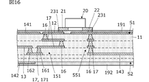
- FIGS. 13 to 17 are sectional views of a transmission line according to another embodiment.
- the connection portion 151 detours to the second main surface S2 side in order to avoid unnecessary conduction, coupling, or interference with electronic components and wiring mounted in the substrate 11.
- It may be formed as follows.
- the first connection electrode 171 is arranged between the signal conductor 13 and the ground conductor 142.
- the ground conductor 142 is partially removed and does not overlap at least a portion of the first connection electrode 171. As a result, the capacitance between the first connection electrode 171 and the ground conductor 142 is suppressed.
- FIGS. 13 to 17 the illustration of the electronic components and wiring mounted in the board 11 is omitted.
- the interlayer connecting conductor 16 may be a via hole penetrating a plurality of layers. Further, as shown in FIG. 18, one interlayer connecting conductor 16 may penetrate a plurality of insulator layers 511, 512 formed of different types of resin sheets. As shown in FIGS. 14 to 17, the connecting portion 151 may have three or more interlayer connecting conductors 16 and a plurality of connecting electrodes 17. As shown in FIG. 17, the connecting portion 151 may have an interlayer connecting conductor 16 that overlaps in a plan view. Further, as shown in FIG. 17, the ground conductor 142 may be formed in the inner layer.
- connection electrode 17 of the connection portion 151 does not overlap the connection portion 551 connecting the ground conductor 141 and the ground conductor 143 in a plan view. As described above, it is preferable that the connection electrode 17 of the connection portion 151 does not overlap the wiring portion connected to the ground in a plan view. As a result, the capacitive coupling between the connection electrode 17 of the connection portion 151 and the wiring portion is suppressed.
Landscapes
- Engineering & Computer Science (AREA)
- Microelectronics & Electronic Packaging (AREA)
- Physics & Mathematics (AREA)
- Electromagnetism (AREA)
- Structure Of Printed Boards (AREA)
- Waveguides (AREA)
Priority Applications (3)
| Application Number | Priority Date | Filing Date | Title |
|---|---|---|---|
| CN202190000455.7U CN218827761U (zh) | 2020-05-15 | 2021-05-11 | 传输线路 |
| JP2022521921A JP7197057B2 (ja) | 2020-05-15 | 2021-05-11 | 伝送線路 |
| US17/983,444 US12191553B2 (en) | 2020-05-15 | 2022-11-09 | Transmission line |
Applications Claiming Priority (2)
| Application Number | Priority Date | Filing Date | Title |
|---|---|---|---|
| JP2020-085754 | 2020-05-15 | ||
| JP2020085754 | 2020-05-15 |
Related Child Applications (1)
| Application Number | Title | Priority Date | Filing Date |
|---|---|---|---|
| US17/983,444 Continuation US12191553B2 (en) | 2020-05-15 | 2022-11-09 | Transmission line |
Publications (1)
| Publication Number | Publication Date |
|---|---|
| WO2021230224A1 true WO2021230224A1 (ja) | 2021-11-18 |
Family
ID=78525887
Family Applications (1)
| Application Number | Title | Priority Date | Filing Date |
|---|---|---|---|
| PCT/JP2021/017809 Ceased WO2021230224A1 (ja) | 2020-05-15 | 2021-05-11 | 伝送線路 |
Country Status (4)
| Country | Link |
|---|---|
| US (1) | US12191553B2 (https=) |
| JP (1) | JP7197057B2 (https=) |
| CN (1) | CN218827761U (https=) |
| WO (1) | WO2021230224A1 (https=) |
Families Citing this family (1)
| Publication number | Priority date | Publication date | Assignee | Title |
|---|---|---|---|---|
| JP2025069696A (ja) * | 2023-10-18 | 2025-05-01 | キヤノン株式会社 | 伝送装置及び伝送システム |
Citations (4)
| Publication number | Priority date | Publication date | Assignee | Title |
|---|---|---|---|---|
| JP2002184898A (ja) * | 2000-10-04 | 2002-06-28 | Murata Mfg Co Ltd | 高周波モジュール |
| JP2007287916A (ja) * | 2006-04-17 | 2007-11-01 | Fujitsu Ltd | 電子部品パッケージ |
| WO2014050238A1 (ja) * | 2012-09-28 | 2014-04-03 | 株式会社村田製作所 | 信号線路モジュールおよび通信端末装置 |
| WO2019189050A1 (ja) * | 2018-03-30 | 2019-10-03 | 株式会社村田製作所 | アンテナモジュールおよびそれを搭載した通信装置 |
Family Cites Families (10)
| Publication number | Priority date | Publication date | Assignee | Title |
|---|---|---|---|---|
| JP4004048B2 (ja) * | 2003-04-11 | 2007-11-07 | Tdk株式会社 | 高周波伝送線路 |
| JP4574322B2 (ja) | 2004-10-21 | 2010-11-04 | 大日本印刷株式会社 | インピーダンスコントロール配線板の製造方法 |
| JP2009004809A (ja) | 2008-09-16 | 2009-01-08 | Kyocera Corp | 配線基板 |
| JP5730152B2 (ja) | 2011-07-26 | 2015-06-03 | 京セラサーキットソリューションズ株式会社 | 配線基板 |
| WO2016163436A1 (ja) | 2015-04-09 | 2016-10-13 | 株式会社村田製作所 | 複合伝送線路および電子機器 |
| CN207009625U (zh) | 2015-09-25 | 2018-02-13 | 株式会社村田制作所 | 天线模块以及电子设备 |
| JP6950747B2 (ja) * | 2017-11-16 | 2021-10-13 | 株式会社村田製作所 | 樹脂多層基板、電子部品およびその実装構造 |
| JP2019106680A (ja) | 2017-12-14 | 2019-06-27 | 日本電信電話株式会社 | 高周波伝送線路 |
| CN217062469U (zh) * | 2019-10-02 | 2022-07-26 | 株式会社村田制作所 | 传输线路以及电路基板 |
| JP7180788B2 (ja) * | 2019-11-15 | 2022-11-30 | 株式会社村田製作所 | 伝送線路及び電子機器 |
-
2021
- 2021-05-11 WO PCT/JP2021/017809 patent/WO2021230224A1/ja not_active Ceased
- 2021-05-11 JP JP2022521921A patent/JP7197057B2/ja active Active
- 2021-05-11 CN CN202190000455.7U patent/CN218827761U/zh active Active
-
2022
- 2022-11-09 US US17/983,444 patent/US12191553B2/en active Active
Patent Citations (4)
| Publication number | Priority date | Publication date | Assignee | Title |
|---|---|---|---|---|
| JP2002184898A (ja) * | 2000-10-04 | 2002-06-28 | Murata Mfg Co Ltd | 高周波モジュール |
| JP2007287916A (ja) * | 2006-04-17 | 2007-11-01 | Fujitsu Ltd | 電子部品パッケージ |
| WO2014050238A1 (ja) * | 2012-09-28 | 2014-04-03 | 株式会社村田製作所 | 信号線路モジュールおよび通信端末装置 |
| WO2019189050A1 (ja) * | 2018-03-30 | 2019-10-03 | 株式会社村田製作所 | アンテナモジュールおよびそれを搭載した通信装置 |
Also Published As
| Publication number | Publication date |
|---|---|
| US12191553B2 (en) | 2025-01-07 |
| JP7197057B2 (ja) | 2022-12-27 |
| CN218827761U (zh) | 2023-04-07 |
| US20230066411A1 (en) | 2023-03-02 |
| JPWO2021230224A1 (https=) | 2021-11-18 |
Similar Documents
| Publication | Publication Date | Title |
|---|---|---|
| JP5811306B1 (ja) | 信号伝送部品および電子機器 | |
| US20220200116A1 (en) | Transmission line and electronic device | |
| WO2011007659A1 (ja) | 信号線路及びその製造方法 | |
| JP2015005744A (ja) | フレキシブル回路板の差動モード信号伝送線のための減衰低減用接地構造体 | |
| US20180070435A1 (en) | Multilayer resin substrate, and method of manufacturing multilayer resin substrate | |
| JP5323435B2 (ja) | 差動伝送用多層配線基板 | |
| US9949368B2 (en) | Resin substrate and electronic device | |
| US9444126B2 (en) | High-frequency signal line | |
| WO2011016192A1 (ja) | 回路基板 | |
| US20210204403A1 (en) | Multilayer board | |
| WO2014021372A1 (ja) | フラットケーブル | |
| JP7001154B2 (ja) | 伝送線路及びその実装構造 | |
| WO2021230224A1 (ja) | 伝送線路 | |
| US9583809B2 (en) | High-frequency signal line | |
| JP7205667B2 (ja) | 信号伝送線路 | |
| WO2020129827A1 (ja) | 多層基板 | |
| JP7708219B2 (ja) | 伝送線路およびそれを備える電子機器 | |
| JP7768019B2 (ja) | シールドフラットケーブル | |
| JPWO2022113779A5 (https=) | ||
| WO2024257449A1 (ja) | 積層基板、ケーブル及び電子機器 | |
| WO2021206019A1 (ja) | 多層基板およびその製造方法 | |
| JPWO2023132309A5 (https=) | ||
| WO2015186537A1 (ja) | 伝送線路部材 | |
| WO2021025073A1 (ja) | 多層基板の製造方法及び多層基板 | |
| WO2018211897A1 (ja) | 複合多層基板 |
Legal Events
| Date | Code | Title | Description |
|---|---|---|---|
| 121 | Ep: the epo has been informed by wipo that ep was designated in this application |
Ref document number: 21804538 Country of ref document: EP Kind code of ref document: A1 |
|
| ENP | Entry into the national phase |
Ref document number: 2022521921 Country of ref document: JP Kind code of ref document: A |
|
| NENP | Non-entry into the national phase |
Ref country code: DE |
|
| 122 | Ep: pct application non-entry in european phase |
Ref document number: 21804538 Country of ref document: EP Kind code of ref document: A1 |