WO2021215237A1 - パルス受信回路、信号伝達装置 - Google Patents
パルス受信回路、信号伝達装置 Download PDFInfo
- Publication number
- WO2021215237A1 WO2021215237A1 PCT/JP2021/014584 JP2021014584W WO2021215237A1 WO 2021215237 A1 WO2021215237 A1 WO 2021215237A1 JP 2021014584 W JP2021014584 W JP 2021014584W WO 2021215237 A1 WO2021215237 A1 WO 2021215237A1
- Authority
- WO
- WIPO (PCT)
- Prior art keywords
- potential
- transformer
- pulse
- signal
- low
- Prior art date
- Legal status (The legal status is an assumption and is not a legal conclusion. Google has not performed a legal analysis and makes no representation as to the accuracy of the status listed.)
- Ceased
Links
Images


Classifications
-
- H—ELECTRICITY
- H02—GENERATION; CONVERSION OR DISTRIBUTION OF ELECTRIC POWER
- H02M—APPARATUS FOR CONVERSION BETWEEN AC AND AC, BETWEEN AC AND DC, OR BETWEEN DC AND DC, AND FOR USE WITH MAINS OR SIMILAR POWER SUPPLY SYSTEMS; CONVERSION OF DC OR AC INPUT POWER INTO SURGE OUTPUT POWER; CONTROL OR REGULATION THEREOF
- H02M1/00—Details of apparatus for conversion
- H02M1/08—Circuits specially adapted for the generation of control voltages for semiconductor devices incorporated in static converters
-
- H—ELECTRICITY
- H01—ELECTRIC ELEMENTS
- H01F—MAGNETS; INDUCTANCES; TRANSFORMERS; SELECTION OF MATERIALS FOR THEIR MAGNETIC PROPERTIES
- H01F19/00—Fixed transformers or mutual inductances of the signal type
- H01F19/04—Transformers or mutual inductances suitable for handling frequencies considerably beyond the audio range
- H01F19/08—Transformers having magnetic bias, e.g. for handling pulses
-
- H—ELECTRICITY
- H01—ELECTRIC ELEMENTS
- H01F—MAGNETS; INDUCTANCES; TRANSFORMERS; SELECTION OF MATERIALS FOR THEIR MAGNETIC PROPERTIES
- H01F27/00—Details of transformers or inductances, in general
- H01F27/28—Coils; Windings; Conductive connections
- H01F27/2804—Printed windings
-
- H—ELECTRICITY
- H02—GENERATION; CONVERSION OR DISTRIBUTION OF ELECTRIC POWER
- H02M—APPARATUS FOR CONVERSION BETWEEN AC AND AC, BETWEEN AC AND DC, OR BETWEEN DC AND DC, AND FOR USE WITH MAINS OR SIMILAR POWER SUPPLY SYSTEMS; CONVERSION OF DC OR AC INPUT POWER INTO SURGE OUTPUT POWER; CONTROL OR REGULATION THEREOF
- H02M1/00—Details of apparatus for conversion
- H02M1/0003—Details of control, feedback or regulation circuits
- H02M1/0006—Arrangements for supplying an adequate voltage to the control circuit of converters
-
- H—ELECTRICITY
- H02—GENERATION; CONVERSION OR DISTRIBUTION OF ELECTRIC POWER
- H02M—APPARATUS FOR CONVERSION BETWEEN AC AND AC, BETWEEN AC AND DC, OR BETWEEN DC AND DC, AND FOR USE WITH MAINS OR SIMILAR POWER SUPPLY SYSTEMS; CONVERSION OF DC OR AC INPUT POWER INTO SURGE OUTPUT POWER; CONTROL OR REGULATION THEREOF
- H02M1/00—Details of apparatus for conversion
- H02M1/0064—Magnetic structures combining different functions, e.g. storage, filtering or transformation
-
- H—ELECTRICITY
- H02—GENERATION; CONVERSION OR DISTRIBUTION OF ELECTRIC POWER
- H02M—APPARATUS FOR CONVERSION BETWEEN AC AND AC, BETWEEN AC AND DC, OR BETWEEN DC AND DC, AND FOR USE WITH MAINS OR SIMILAR POWER SUPPLY SYSTEMS; CONVERSION OF DC OR AC INPUT POWER INTO SURGE OUTPUT POWER; CONTROL OR REGULATION THEREOF
- H02M3/00—Conversion of DC power input into DC power output
- H02M3/003—Constructional details, e.g. physical layout, assembly, wiring or busbar connections
-
- H—ELECTRICITY
- H03—ELECTRONIC CIRCUITRY
- H03K—PULSE TECHNIQUE
- H03K19/00—Logic circuits, i.e. having at least two inputs acting on one output; Inverting circuits
- H03K19/0175—Coupling arrangements; Interface arrangements
-
- H—ELECTRICITY
- H04—ELECTRIC COMMUNICATION TECHNIQUE
- H04L—TRANSMISSION OF DIGITAL INFORMATION, e.g. TELEGRAPHIC COMMUNICATION
- H04L25/00—Baseband systems
- H04L25/02—Details ; arrangements for supplying electrical power along data transmission lines
- H04L25/0264—Arrangements for coupling to transmission lines
- H04L25/0266—Arrangements for providing Galvanic isolation, e.g. by means of magnetic or capacitive coupling
-
- H—ELECTRICITY
- H01—ELECTRIC ELEMENTS
- H01F—MAGNETS; INDUCTANCES; TRANSFORMERS; SELECTION OF MATERIALS FOR THEIR MAGNETIC PROPERTIES
- H01F19/00—Fixed transformers or mutual inductances of the signal type
- H01F19/04—Transformers or mutual inductances suitable for handling frequencies considerably beyond the audio range
- H01F19/08—Transformers having magnetic bias, e.g. for handling pulses
- H01F2019/085—Transformer for galvanic isolation
-
- H—ELECTRICITY
- H02—GENERATION; CONVERSION OR DISTRIBUTION OF ELECTRIC POWER
- H02M—APPARATUS FOR CONVERSION BETWEEN AC AND AC, BETWEEN AC AND DC, OR BETWEEN DC AND DC, AND FOR USE WITH MAINS OR SIMILAR POWER SUPPLY SYSTEMS; CONVERSION OF DC OR AC INPUT POWER INTO SURGE OUTPUT POWER; CONTROL OR REGULATION THEREOF
- H02M1/00—Details of apparatus for conversion
- H02M1/44—Circuits or arrangements for compensating for electromagnetic interference in converters or inverters
Definitions
- the invention disclosed in this specification relates to a pulse receiving circuit and a signal transmitting device.
- Patent Document 1 by the applicant of the present application can be mentioned.
- the invention disclosed in the present specification includes a signal transmission device that is not easily affected by common mode noise, and a pulse receiving circuit used for the signal transmission device.
- the purpose is to provide.
- the signal transmission device disclosed in the present specification receives a differential input of a first received pulse signal appearing in the secondary winding of the first transformer and a second received pulse signal appearing in the secondary winding of the second transformer.
- a first pulse detector that accepts, a second pulse detector that accepts differential inputs of the first received pulse signal and the second received pulse signal with an input polarity opposite to that of the first pulse detector, and the first pulse detector.
- the configuration includes a pulse detector and a logic unit that generates a received pulse signal based on the output signals of each of the second pulse detectors.
- FIG. 1 is a diagram showing an application example of a signal transmission device.
- FIG. 2 is a diagram showing a first embodiment of a signal transmission device.
- FIG. 3 is a diagram showing an example of the noise removing operation in the first embodiment.
- FIG. 4 is a diagram showing a second embodiment of the signal transmission device.
- FIG. 5 is a diagram showing an example of a noise removing operation in the second embodiment.
- FIG. 6 is a diagram showing an example of comparative operation of the comparator.
- FIG. 7 is a diagram showing a structural example of the transchip according to the second embodiment.
- FIG. 8 is a diagram showing a two-channel signal transmission device.
- FIG. 9 is a perspective view of the semiconductor device used as the transformer chip shown in FIG. FIG.
- FIG. 10 is a plan view of the semiconductor device shown in FIG.
- FIG. 11 is a plan view showing a layer in which a low potential coil is formed in the semiconductor device shown in FIG.
- FIG. 12 is a plan view showing a layer in which a high potential coil is formed in the semiconductor device shown in FIG.
- FIG. 13 is a cross-sectional view taken along the line VIII-VIII shown in FIG.
- FIG. 14 is a cross-sectional view taken along the line IX-IX shown in FIG.
- FIG. 15 is an enlarged view of the region X shown in FIG.
- FIG. 16 is an enlarged view of the region XI shown in FIG.
- FIG. 17 is an enlarged view of the region XII shown in FIG.
- FIG. 18 is an enlarged view of the region XIII shown in FIG. 13 and is a diagram showing a separated structure.
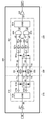
- FIG. 1 is a diagram showing an example of an application using a signal transmission device.
- the signal transmission device 200 of this configuration example changes from the primary circuit system (VCC1-GND1 system) to the secondary circuit system (VCC2-GND2 system) while electrically insulating the primary circuit system and the secondary circuit system.
- It is a semiconductor integrated circuit device (so-called insulated gate driver IC) that transmits a pulse signal and drives the gate of a transistor provided in a secondary circuit system.
- the signal transmission device 200 has a plurality of external terminals (in this figure, input terminals INA and INB, output terminals OUT, power supply terminals VCS1 and VCS2, ground terminals GND1 and GND2) as means for establishing an electrical connection with the outside of the device.
- external terminals in this figure, input terminals INA and INB, output terminals OUT, power supply terminals VCS1 and VCS2, ground terminals GND1 and GND2
- N-channel type MOS [metal oxide semiconductor] field effect transistor N1, capacitors C1 and C2, resistor R1 are externally attached to their external terminals.
- the ground terminal GND1, the power supply terminal VCS1, the input terminal INA, the input terminal INB, and the ground terminal GND1 are arranged in order from the top. Has been done.
- the ground terminal GND2, the power supply terminal VCS2, the output terminal OUT, and the ground are in order from the top.
- the terminals GND2 are arranged.
- the external terminals (GND1, VCS1, INA and INB) of the primary circuit system are integrated on the first side of the package, and the external terminals (GND2, VCS2, OUT) of the secondary circuit system are the second side of the package. It is good to concentrate on the sides.
- ground terminals GND1 and GND2 are arranged at both ends of the first side and the second side of the package, respectively. That is, it is preferable to provide two ground terminals GND1 and two respectively.
- the power supply terminal VCS1 is connected to the power supply line of the primary circuit system. Both of the two ground terminals GND1 are connected to the ground line of the primary circuit system. A capacitor C1 is connected between the power supply line and the ground line of the primary circuit system. Two input signals (for example, one is a gate control signal and the other is an enable signal) are input to the input terminals INA and INB, respectively.
- the power supply terminal VCS2 is connected to the power supply line of the secondary circuit system. Both of the two ground terminals GND2 are connected to the ground line of the secondary circuit system.
- a capacitor C2 is connected between the power supply line and the ground line of the secondary circuit system.
- the first end of the resistor R1 is connected to the output terminal OUT.
- the second end of the resistor R2 is connected to the gate of the transistor N1.
- the controller chip 210 is a semiconductor chip that operates by being supplied with a power supply voltage VCS1 (for example, a maximum of 7 V based on GND1).
- VCS1 power supply voltage
- the controller chip 210 integrates, for example, Schmidt buffers 211A and 211B, an AND gate 211C, a pulse transmission circuit 212, and a low voltage protection circuit 213.
- the Schmidt buffer 211A is an example of waveform shaping means, and is connected between the input terminal INA and the first input end (non-inverting input end) of the AND gate 211C.
- the Schmidt buffer 211B is an example of waveform shaping means, and is connected between the input terminal INB and the second input end (inverted input end) of the AND gate 211C.
- the pulse transmission circuit 212 generates transmission pulse signals S1 and S2 in response to the input pulse signal S0. More specifically, when notifying that the input pulse signal S0 is at a high level, the pulse transmission circuit 212 performs pulse drive (single or multiple transmission pulse output) of the transmission pulse signal S1 to perform an input pulse. When notifying that the signal S0 is at a low level, the transmission pulse signal S2 is pulse-driven. That is, the pulse transmission circuit 212 pulse-drives either one of the transmission pulse signals S1 and S2 according to the logic level of the input pulse signal S0.
- the low voltage protection circuit 213 prevents malfunction at the time of low voltage input by putting the controller chip 210 in the standby state until the power supply voltage VCS1 reaches the UVLO [under voltage lock out] release voltage.
- the driver chip 220 is a semiconductor chip that operates by being supplied with a power supply voltage VCS2 (for example, a maximum of 30 V based on GND2).
- VCS2 for example, a maximum of 30 V based on GND2
- the driver chip 220 integrates, for example, a pulse receiving circuit 221, a driver 222, and a low voltage protection circuit 223.
- the pulse receiving circuit 221 generates a received pulse signal S5 in response to the received pulse signals S3 and S4 input from the transformer chip 230. More specifically, the pulse receiving circuit 221 receives the pulse drive of the received pulse signal S3 to lower the received pulse signal S5 to a low level, while receives the pulse drive of the received pulse signal S4 to generate the received pulse signal S5. Launch to a high level. That is, the pulse reception circuit 221 switches the logic level of the reception pulse signal S5 according to the logic level of the input pulse signal S0.
- CMOS complementary MOS
- the source of the transistor 222H is connected to the power supply terminal VCS2.
- the source of the transistor 222L is connected to the ground terminal GND2.
- the drains of the transistors 222H and 222L are both connected to the output terminal OUT.
- the low voltage protection circuit 223 prevents malfunction at the time of low voltage input by putting the driver chip 220 in the standby state until the power supply voltage VCS2 reaches the UVLO release voltage.
- the transformer chip 230 receives the transmission pulse signals S1 and S2 input from the pulse transmission circuit 212, respectively, while insulating the controller chip 210 and the driver chip 220 in a DC manner by using the transformers 231 and 232, respectively. And S4 are output to the pulse receiving circuit 221.
- the transformer 231 outputs the reception pulse signal S3 from the secondary winding 231s in response to the transmission pulse signal S1 input to the primary winding 231p.
- the transformer 232 outputs the reception pulse signal S4 from the secondary winding 232s in response to the transmission pulse signal S2 input to the primary winding 232p.
- the signal transmission device 200 of this configuration example independently has a transformer chip 230 on which only the transformers 231 and 232 are mounted, and these three chips are used as a single unit. It is sealed in a package.
- both the controller chip 210 and the driver chip 220 can be formed by a general low withstand voltage to medium withstand voltage process (withstand voltage of several V to several tens of V), and thus are dedicated. It is not necessary to use a high withstand voltage process (withstand voltage of several kV), and the manufacturing cost can be reduced.
- controller chip 210 and the driver chip 220 can both be created by an existing process with a proven track record, and there is no need to perform a new reliability test, so that the development period can be shortened and the development cost can be reduced. It can contribute to the reduction.
- the controller chip 210 and the driver chip 220 can be used. There is no need to redevelop, which can contribute to shortening the development period and reducing development costs.
- FIG. 2 is a diagram showing a first embodiment of the signal transmission device 200.
- the circuit configurations of the pulse transmitting circuit 212 and the pulse receiving circuit 221 are specifically depicted based on FIG. 1 described above.
- the above-mentioned input terminals INA and INB have been replaced with a single input terminal IN.
- the Schmidt buffers 211A and 211B and the AND gate 211C described above have been replaced with a single Schmidt buffer 211.
- the description of each of the transistors 222H and 222L described above is omitted.
- external terminals T11 to T18 are clearly indicated on the transformer chip 230.
- the primary winding 231p of the transformer 231 is connected between the external terminal T11 and the external terminal T12.
- the primary winding 232p of the transformer 232 is connected between the external terminal T13 and the external terminal T14.
- the secondary winding 231s of the transformer 231 is connected between the external terminal T15 and the external terminal T16.
- the secondary winding 232s of the transformer 232 is connected between the external terminal T17 and the external terminal T18.
- parasitic capacitances are attached between the primary winding 231p and the secondary winding 231s and between the primary winding 232p and the secondary winding 232s, respectively. ing.
- the pulse transmission circuit 212 includes a logic unit 212a, buffers 212b and 212c, and diodes 212d and 212e.
- the logic unit 212a drives the buffers 212b and 212c in response to the input pulse signal S0 (which corresponds to the input pulse signal IN). More specifically, the logic unit 212a drives the buffer 212b when notifying that the input pulse signal S0 is at a high level, while the logic unit 212a is a buffer when notifying that the input pulse signal S0 is at a low level. Drives 212c.
- the buffer 212b is driven by the logic unit 212a to generate a transmission pulse signal S1 and outputs this to the external terminal T11 of the transformer chip 230.
- the buffer 212c is driven by the logic unit 212a to generate a transmission pulse signal S2, which is output to the external terminal T13 of the transformer chip 230.
- the diode 212d is an example of an electrostatic protection element in which the cathode is connected to the external terminal T11 of the transformer chip 230 and the anode is connected to the external terminals T12 and T14 of the transformer chip 230.
- the diode 212e is an example of an electrostatic protection element in which the cathode is connected to the external terminals T13 of the transformer chip 230 and the anode is connected to the external terminals T12 and T14 of the transformer chip 230.
- the pulse receiving circuit 221 includes diodes 221a and 221b, buffers 221c to 221f, delay units 221g and 221h, AND gates 221i and 221j, and a logic unit 221k.
- the cathode of the diode 221a is connected to the external terminal T15 of the transformer chip 230.
- the anode of the diode 221a is connected to the external terminals T16 and T18 of the transformer chip 230.
- the diode 221a connected in this way functions as an electrostatic protection element connected between both ends of the secondary winding 231s forming the transformer 231.
- the cathode of the diode 221b is connected to the external terminal T17 of the transformer chip 230.
- the anode of the diode 221b is connected to the external terminals T16 and T18 of the transformer chip 230.
- the diode 221b connected in this way functions as an electrostatic protection element connected between both ends of the secondary winding 232s forming the transformer 232.
- the internal signal s17 is lowered to a low level.
- the internal signal s14 is lowered to a low level.
- the internal signal s15 corresponds to, for example, a set signal of the logic unit 221k.
- the internal signal s15 corresponds to, for example, the reset signal of the logic unit 221k.
- the logic unit 221k generates a received pulse signal S5 (and thus an output pulse signal OUT) based on the internal signals s15 and s18. Specifically, for example, the logic unit 221k sets the received pulse signal S5 to a high level when the internal signal s15 rises to a high level, and the received pulse signal S5 when the internal signal s18 rises to a high level. Reset to low level.
- the buffers 221c to 221f, the delay portions 221g and 221h, and the AND gates 221i and 221j are received pulse signals S3 via the propagation paths indicated by the thin arrows in the figure. It functions as a noise canceller for removing common mode noise superimposed on S4 and S4, respectively.
- FIG. 3 is a diagram showing an example of the noise removing operation in the first embodiment, and the input pulse signal IN, the internal signals s11 to s18, and the output pulse signal OUT are depicted in order from the top.
- the output pulse signal OUT is set to a high level.
- no inconsistency occurs at time t12, since the internal signal s18 should be originally maintained at the low level, no inconsistency occurs.
- the output pulse signal OUT is reset to the low level.
- no inconsistency occurs at time t16.
- the threshold voltage Vth of the buffers 221c to 221f formed by the CMOS circuit is high, and a large amount of energy is required for signal transmission, so that the emission noise and the power consumption become large. Further, if the threshold voltage Vth of the buffers 221c to 221f is simply lowered, a malfunction is likely to occur due to noise. Therefore, in the following, a new second embodiment capable of solving such a problem will be proposed.
- FIG. 4 is a diagram showing a second embodiment of the signal transmission device 200.
- the pulse receiving circuit 221 of the present embodiment includes diodes 221A and 221B, N-channel MOS field effect transistors 221C and 221D, comparators 221E and 221F, a timer 221G, and a logic unit 221H.
- the cathode of the diode 221A is connected to the external terminal T24 of the transformer chip 230.
- the anode of the diode 221A is connected to the external terminal T25 of the transformer chip 230.
- the diode 221A connected in this way functions as a first electrostatic protection element connected between both ends of the secondary winding 231s forming the transformer 231.
- the cathode of the diode 221B is connected to the external terminal T26 of the transformer chip 230.
- the anode of the diode 221B is connected to the external terminal T25 of the transformer chip 230.
- the diode 221B connected in this way functions as a second electrostatic protection element connected between both ends of the secondary winding 232s forming the transformer 232.
- the drain of the transistor 221C is connected to the external terminal T24 of the transformer chip 230.
- the source of the transistor 221C is connected to the external terminal T25 of the transformer chip 230.
- the transistor 221C connected in this way functions as a first switch connected between both ends of the secondary winding 231s forming the transformer 231.
- the drain of the transistor 221D is connected to the external terminal T26 of the transformer chip 230.
- the source of the transistor 221D is connected to the external terminal T25 of the transformer chip 230.
- the transistor 221D connected in this way functions as a second switch connected between both ends of the secondary winding 232s forming the transformer 232.
- the non-inverting input end (+) of the comparator 221E is connected to the external terminal T24 of the transformer chip 230.
- the inverting input end ( ⁇ ) of the comparator 221E is connected to the external terminal T26 of the transformer chip 230.
- the internal signal s23 corresponds to, for example, the set signal of the logic unit 221H, and becomes a high level when s21> s22 and a low level when s21 ⁇ s22.
- the non-inverting input end (+) of the comparator 221F is connected to the external terminal T26 of the transformer chip 230.
- the inverting input end ( ⁇ ) of the comparator 221F is connected to the external terminal T24 of the transformer chip 230.
- the second pulse detector that produces s24 corresponds to, for example, the reset signal of the logic unit 221H, and becomes a low level when s21> s22 and a high level when s21 ⁇ s22.
- Transistors 221C and 221D are turned on by setting the internal signal s25 to a high level over tm2.
- the logic unit 221H generates a received pulse signal S5 (and thus an output pulse signal OUT) based on the internal signals s23 and s24. Specifically, for example, the logic unit 221H sets the received pulse signal S5 to a high level when the internal signal s23 rises to a high level, and the received pulse signal S5 when the internal signal s24 rises to a high level. Reset to low level.
- FIG. 5 is a diagram showing an example of the noise removing operation in the second embodiment, and the input pulse signal IN, the internal signals s21 to s25, and the output pulse signal OUT are depicted in order from the top.
- the threshold voltage Vth of the pulse receiving circuit 221 (in this figure, the comparator 221E) is compared with the first embodiment (FIG. 2) described above. Since the input offset voltages Vofs1 and Voffs2) of 221F and 221F can be set small, it is possible to remove the common mode noise while suppressing the emission noise and the power consumption.
- the internal signal s25 is set to a high level for a predetermined mask time tm2.
- the transistors 221C and 221D are turned on, and both ends of the secondary windings 231s and 232s are short-circuited, so that the differential inputs of the comparators 221E and 221F are zero.
- unnecessary pulse generation of the internal signals s23 and s24 is suppressed.
- the comparators 221E and 221F are circuit-designed to have input offset voltages Vofs1 and Vofs2, respectively. That is, the internal signal s23 has a high level when COMP1> Vofs1 and a low level when COMP1 ⁇ Vofs1. Further, the internal signal s24 has a high level when COMP2> Vofs2 and a low level when COMP2 ⁇ Vofs2.
- the primary winding 231p of the transformer 231 is connected between the external terminal T21 and the external terminal T22.
- the primary winding 232p of the transformer 232 is connected between the external terminal T23 and the external terminal T22.
- the secondary winding 231s of the transformer 231 is connected between the external terminal T24 and the external terminal T25.
- the secondary winding 232s of the transformer 232 is connected between the external terminal T26 and the external terminal T25.
- the transformer chip 230 has an external terminal T21 to which the first end of the primary winding 231p is connected, and an external terminal T22 to which the second end of the primary winding 231p and the first end of the primary winding 232p are connected.
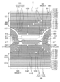
- FIG. 7 is a diagram showing a structural example of the transchip 230 according to the second embodiment.
- the transformer 231 includes a primary winding 231p and a secondary winding 231s facing each other in the vertical direction.
- the transformer 232 includes a primary winding 232p and a secondary winding 232s facing each other in the vertical direction.
- the primary windings 231p and 232p are both formed in the first layer (lower layer) 230a of the transformer chip 230, and the secondary windings 231s and 232s are both formed in the second layer (upper layer) 230b of the transformer chip 230. It is formed.
- the secondary winding 231s is arranged directly above the primary winding 231p and faces the primary winding 231p. Further, the secondary winding 232s is arranged directly above the primary winding 232p and faces the primary winding 232p.
- the primary winding 231p is laid spirally starting from the first end connected to the internal terminal X21 so as to surround the circumference of the internal terminal X21 in a clockwise direction, and the second end corresponding to the end point is inside. It is connected to terminal X22.
- the primary winding 232p is spirally laid so as to surround the circumference of the internal terminal X23 in a counterclockwise direction starting from the first end connected to the internal terminal X23, and the second winding corresponding to the end point thereof.
- the end is connected to the internal terminal X22.
- the internal terminals X21, X22, and X23 are arranged linearly in the order shown in the drawing.
- the internal terminal X21 is connected to the external terminal T21 of the second layer 230b via the conductive wiring Y21 and the via Z21.
- the internal terminal X22 is connected to the external terminal T22 of the second layer 230b via the conductive wiring Y22 and the via Z22.
- the internal terminal X23 is connected to the external terminal T23 of the second layer 230b via the conductive wiring Y23 and the via Z23.
- the external terminals T21 to T23 are arranged linearly side by side and are used for wire bonding with the controller chip 210.
- the secondary winding 231s is spirally laid so as to surround the outer terminal T24 in a counterclockwise direction starting from the first end connected to the external terminal T24, and the second end corresponding to the end point thereof. Is connected to the external terminal T25.
- the secondary winding 232s is spirally laid so as to surround the outer terminal T26 in a clockwise direction starting from the first end connected to the external terminal T26, and the second winding corresponding to the end point thereof. The end is connected to the external terminal T25.
- the external terminals T24, T25 and T26 are arranged linearly in the order shown in the drawing, and are used for wire bonding with the driver chip 220.
- the secondary windings 231s and 232s are AC-connected to the primary windings 231p and 232p by magnetic coupling, respectively, and are DC-insulated from the primary windings 231p and 232p, respectively. That is, the driver chip 220 is AC-connected to the controller chip 210 via the transformer chip 230, and is DC-insulated from the controller chip 210 by the transformer chip 230.
- FIG. 8 is a diagram showing the signal transmission device 200 having two channels. As shown in this figure, the signal transmission device 200 has two input terminals IN1 and IN2 and two output terminals OUT1 and OUT2, and can perform pulse transmission for two channels. be.
- the signal transmission path from the input terminal IN1 to the output terminal OUT1 via the Schmidt buffer 211 (1), the pulse transmission circuit 212, the transformers 231 and 232, the pulse reception circuit 221 and the driver 222 (1) is the first.
- the signal transmission path from the input terminal IN2 to the output terminal OUT2 via the Schmidt buffer 211 (2), the pulse transmission circuit 212, the transformers 233 and 234, the pulse reception circuit 221 and the driver 222 (2) is the second. For channels.
- transformer chip 230 is provided with transformers 233 and 234 for the second channel and external terminals T31 to T36 in addition to the transformers 231 and 232 for the first channel and the external terminals T21 to T26.
- the primary winding 233p of the transformer 233 is connected between the external terminal T31 and the external terminal T32.
- the primary winding 234p of the transformer 234 is connected between the external terminal T33 and the external terminal T32.
- the secondary winding 233s of the transformer 233 is connected between the external terminal T34 and the external terminal T35.
- the secondary winding 234s of the transformer 234 is connected between the external terminal T36 and the external terminal T35.
- the external terminal T31 to which the first end of the primary winding 233p is connected, and the second end and the primary winding of the primary winding 233p are connected.
- FIG. 9 is a perspective view showing a semiconductor device 5 used as the transformer chip 230 shown in FIG.
- FIG. 10 is a plan view of the semiconductor device 5 shown in FIG.
- FIG. 10 is a plan view of the semiconductor device 5 shown in FIG.
- FIG. 13 is a cross-sectional view taken along the line VIII-VIII shown in FIG.
- FIG. 14 is a cross-sectional view taken along the line IX-IX shown in FIG.
- FIG. 15 is an enlarged view of the region X shown in FIG.
- FIG. 16 is an enlarged view of the region XI shown in FIG.
- FIG. 17 is an enlarged view of the region XII shown in FIG.
- FIG. 18 is an enlarged view of the region XIII shown in FIG. 13 and shows the separation structure 130.
- the semiconductor device 5 includes a rectangular parallelepiped semiconductor chip 41.
- the semiconductor chip 41 includes at least one of silicon, a wide bandgap semiconductor and a compound semiconductor.
- the wide bandgap semiconductor is composed of a semiconductor that exceeds the bandgap of silicon (about 1.12 eV). Wide bandgap The bandgap of the semiconductor is preferably 2.0 eV or more.
- the wide bandgap semiconductor may be SiC (silicon carbide).
- the compound semiconductor may be a group III-V compound semiconductor.
- the compound semiconductor may contain at least one of AlN (aluminum nitride), InN (indium nitride), GaN (gallium nitride) and GaAs (gallium arsenide).
- the semiconductor chip 41 includes a semiconductor substrate made of silicon in this form.
- the semiconductor chip 41 may be an epitaxial substrate having a laminated structure including a silicon semiconductor substrate and a silicon epitaxial layer.
- the conductive type of the semiconductor substrate may be n type or p type.
- the epitaxial layer may be n-type or p-type.
- the semiconductor chip 41 has a first main surface 42 on one side, a second main surface 43 on the other side, and chip side walls 44A to 44D connecting the first main surface 42 and the second main surface 43.
- the first main surface 42 and the second main surface 43 are formed in a rectangular shape (rectangular shape in this form) in a plan view (hereinafter, simply referred to as “planar view”) viewed from their normal direction Z. ..
- the chip side walls 44A to 44D include a first chip side wall 44A, a second chip side wall 44B, a third chip side wall 44C, and a fourth chip side wall 44D.
- the first chip side wall 44A and the second chip side wall 44B form the long side of the semiconductor chip 41.
- the first chip side wall 44A and the second chip side wall 44B extend along the first direction X and face the second direction Y.
- the third chip side wall 44C and the fourth chip side wall 44D form a short side of the semiconductor chip 41.
- the third chip side wall 44C and the fourth chip side wall 44D extend in the second direction Y and face the first direction X.
- the chip side walls 44A to 44D are formed of a ground surface.
- the semiconductor device 5 further includes an insulating layer 51 formed on the first main surface 42 of the semiconductor chip 41.
- the insulating layer 51 has an insulating main surface 52 and insulating side walls 53A to 53D.
- the insulating main surface 52 is formed in a rectangular shape (rectangular shape in this form) that matches the first main surface 42 in a plan view.
- the insulating main surface 52 extends parallel to the first main surface 42.
- the insulating side walls 53A to 53D include a first insulating side wall 53A, a second insulating side wall 53B, a third insulating side wall 53C, and a fourth insulating side wall 53D.
- the insulating side walls 53A to 53D extend from the peripheral edge of the insulating main surface 52 toward the semiconductor chip 41 and are connected to the chip side walls 44A to 44D. Specifically, the insulating side walls 53A to 53D are formed flush with the chip side walls 44A to 44D.
- the insulating side walls 53A to 53D form a flush ground surface on the chip side walls 44A to 44D.
- the insulating layer 51 is composed of a multilayer insulating laminated structure including a lowermost insulating layer 55, an uppermost insulating layer 56, and a plurality of (11 layers in this form) interlayer insulating layers 57.
- the bottom insulating layer 55 is an insulating layer that directly covers the first main surface 42.
- the uppermost insulating layer 56 is an insulating layer that forms an insulating main surface 52.
- the plurality of interlayer insulating layers 57 are insulating layers interposed between the lowermost insulating layer 55 and the uppermost insulating layer 56.
- the bottom insulating layer 55 has a single-layer structure containing silicon oxide.
- the uppermost insulating layer 56 has a single-layer structure containing silicon oxide.
- the thickness of the lowermost insulating layer 55 and the thickness of the uppermost insulating layer 56 may be 1 ⁇ m or more and 3 ⁇ m or less (for example, about 2 ⁇ m), respectively.
- the plurality of interlayer insulating layers 57 each have a laminated structure including a first insulating layer 58 on the lowermost insulating layer 55 side and a second insulating layer 59 on the uppermost insulating layer 56 side.
- the first insulating layer 58 may contain silicon nitride.
- the first insulating layer 58 is formed as an etching stopper layer for the second insulating layer 59.
- the thickness of the first insulating layer 58 may be 0.1 ⁇ m or more and 1 ⁇ m or less (for example, about 0.3 ⁇ m).
- the second insulating layer 59 is formed on the first insulating layer 58. It contains an insulating material different from that of the first insulating layer 58.
- the second insulating layer 59 may contain silicon oxide.
- the thickness of the second insulating layer 59 may be 1 ⁇ m or more and 3 ⁇ m or less (for example, about 2 ⁇ m). The thickness of the second insulating layer 59 preferably exceeds the thickness of the first insulating layer 58.
- the total thickness DT of the insulating layer 51 may be 5 ⁇ m or more and 50 ⁇ m or less.
- the total thickness DT of the insulating layer 51 and the number of layers of the interlayer insulating layer 57 are arbitrary, and are adjusted according to the withstand voltage (dielectric breakdown resistance) to be realized.
- the insulating materials of the lowermost insulating layer 55, the uppermost insulating layer 56, and the interlayer insulating layer 57 are arbitrary and are not limited to a specific insulating material.
- the semiconductor device 5 includes a first functional device 45 formed on the insulating layer 51.
- the first functional device 45 includes one or more (plural in this form) transformers 21. That is, the semiconductor device 5 is composed of a multi-channel type device including a plurality of transformers 21.
- the plurality of transformers 21 are formed in the inner portion of the insulating layer 51 at intervals from the insulating side walls 53A to 53D.
- the plurality of transformers 21 are formed at intervals in the first direction X.
- the plurality of transformers 21 are the first transformer 21A, the second transformer 21B, the third transformer 21C, and the first transformer 21A, the second transformer 21B, and the third transformer 21C formed in this order from the insulating side wall 53C side to the insulating side wall 53D side in a plan view.
- Each of the plurality of transformers 21A to 21D has a similar structure.
- the structure of the first transformer 21A will be described as an example.
- the description of the structure of the second transformer 21B, the third transformer 21C and the fourth transformer 21D the description of the structure of the first transformer 21A shall be applied mutatis mutandis and will be omitted.
- the low potential coil 22 is formed in the insulating layer 51.
- the high-potential coil 23 is formed in the insulating layer 51 so as to face the low-potential coil 22 in the normal direction Z.
- the low-potential coil 22 and the high-potential coil 23 are formed in a region (that is, a plurality of interlayer insulating layers 57) sandwiched between the lowermost insulating layer 55 and the uppermost insulating layer 56.
- the low-potential coil 22 is formed in the insulating layer 51 on the lowermost insulating layer 55 (semiconductor chip 41) side, and the high-potential coil 23 has the uppermost insulating layer 56 in the insulating layer 51 with respect to the low-potential coil 22. It is formed on the (insulating main surface 52) side. That is, the high-potential coil 23 faces the semiconductor chip 41 with the low-potential coil 22 interposed therebetween.
- the location of the low-potential coil 22 and the high-potential coil 23 is arbitrary. Further, the high-potential coil 23 may face the low-potential coil 22 with one or more interlayer insulating layers 57 interposed therebetween.
- the distance between the low-potential coil 22 and the high-potential coil 23 (that is, the number of layers of the interlayer insulating layer 57) is appropriately adjusted according to the insulation withstand voltage and the electric field strength between the low-potential coil 22 and the high-potential coil 23.
- the low-potential coil 22 is formed in the interlayer insulating layer 57, which is the third layer counting from the lowermost insulating layer 55 side.
- the high potential coil 23 is formed in the interlayer insulating layer 57, which is the first layer counting from the uppermost insulating layer 56 side.
- the low-potential coil 22 is embedded in the interlayer insulating layer 57 so as to penetrate the first insulating layer 58 and the second insulating layer 59.
- the low potential coil 22 includes a first inner end 24, a first outer end 25, and a first spiral portion 26 spirally routed between the first inner end 24 and the first outer end 25.
- the first spiral portion 26 is drawn in a spiral shape extending in an elliptical shape (oval shape) in a plan view.
- the portion forming the innermost peripheral edge of the first spiral portion 26 defines the elliptical first inner region 66 in a plan view.
- the number of turns of the first spiral portion 26 may be 5 or more and 30 or less.
- the width of the first spiral portion 26 may be 0.1 ⁇ m or more and 5 ⁇ m or less.
- the width of the first spiral portion 26 is preferably 1 ⁇ m or more and 3 ⁇ m or less.
- the width of the first spiral portion 26 is defined by the width in the direction orthogonal to the spiral direction.
- the first winding pitch of the first spiral portion 26 may be 0.1 ⁇ m or more and 5 ⁇ m or less.
- the first winding pitch is preferably 1 ⁇ m or more and 3 ⁇ m or less.
- the first winding pitch is defined by the distance between two adjacent portions of the first spiral portion 26 in a direction orthogonal to the spiral direction.
- the winding shape of the first spiral portion 26 and the planar shape of the first inner region 66 are arbitrary and are not limited to the shapes shown in FIG. 11 and the like.
- the first spiral portion 26 may be wound into a polygonal shape such as a triangle shape or a quadrangular shape, or a circular shape in a plan view.
- the first inner region 66 may be divided into a polygonal shape such as a triangular shape or a quadrangular shape, or a circular shape in a plan view, depending on the winding shape of the first spiral portion 26.
- the low potential coil 22 may contain at least one of titanium, titanium nitride, copper, aluminum and tungsten.
- the low potential coil 22 may have a laminated structure including a barrier layer and a main body layer.
- the barrier layer partitions the recess space in the interlayer insulating layer 57.
- the main body layer is buried in the recess space partitioned by the barrier layer.
- the barrier layer may contain at least one of titanium and titanium nitride.
- the body layer may contain at least one of copper, aluminum and tungsten.
- the high-potential coil 23 is embedded in the interlayer insulating layer 57 so as to penetrate the first insulating layer 58 and the second insulating layer 59.
- the high potential coil 23 includes a second inner end 27, a second outer end 28, and a second spiral portion 29 spirally routed between the second inner end 27 and the second outer end 28.
- the second spiral portion 29 is drawn in a spiral shape extending in an elliptical shape (oval shape) in a plan view.
- the portion forming the innermost peripheral edge of the second spiral portion 29 partitions the second inner region 67 having an elliptical shape in a plan view.
- the second inner region 67 of the second spiral portion 29 faces the first inner region 66 of the first spiral portion 26 in the normal direction Z.
- the number of turns of the second spiral portion 29 may be 5 or more and 30 or less.
- the number of turns of the second spiral portion 29 with respect to the number of turns of the first spiral portion 26 is adjusted according to the voltage value to be boosted.
- the number of turns of the second spiral portion 29 preferably exceeds the number of turns of the first spiral portion 26.
- the number of turns of the second spiral portion 29 may be less than the number of turns of the first spiral portion 26, or may be equal to the number of turns of the first spiral portion 26.
- the width of the second spiral portion 29 may be 0.1 ⁇ m or more and 5 ⁇ m or less.
- the width of the second spiral portion 29 is preferably 1 ⁇ m or more and 3 ⁇ m or less.
- the width of the second spiral portion 29 is defined by the width in the direction orthogonal to the spiral direction.
- the width of the second spiral portion 29 is preferably equal to the width of the first spiral portion 26.
- the second winding pitch of the second spiral portion 29 may be 0.1 ⁇ m or more and 5 ⁇ m or less.
- the second winding pitch is preferably 1 ⁇ m or more and 3 ⁇ m or less.
- the second winding pitch is defined by the distance between two adjacent portions of the second spiral portion 29 in the direction orthogonal to the spiral direction.
- the second winding pitch is preferably equal to the first winding pitch of the first spiral portion 26.
- the winding shape of the second spiral portion 29 and the planar shape of the second inner region 67 are arbitrary and are not limited to the shapes shown in FIG. 12 and the like.
- the second spiral portion 29 may be wound into a polygonal shape such as a triangle shape or a quadrangular shape, or a circular shape in a plan view.
- the second inner region 67 may be divided into a polygonal shape such as a triangular shape or a quadrangular shape, or a circular shape in a plan view, depending on the winding shape of the second spiral portion 29.
- the high-potential coil 23 is preferably formed of the same conductive material as the low-potential coil 22. That is, the high-potential coil 23 preferably includes a barrier layer and a main body layer, similarly to the low-potential coil 22.
- the plurality of low-potential terminals 11 are electrically connected to the low-potential coils 22 of the corresponding transformers 21A to 21D, respectively.
- the plurality of high-potential terminals 12 are electrically connected to the high-potential coils 23 of the corresponding transformers 21A to 21D, respectively.
- the plurality of low potential terminals 11 are formed on the insulating main surface 52 of the insulating layer 51. Specifically, the plurality of low potential terminals 11 are formed in the region on the insulating side wall 53B side at intervals in the second direction Y from the plurality of transformers 21A to 21D, and are arranged at intervals in the first direction X. Has been done.
- the plurality of low-potential terminals 11 include a first low-potential terminal 11A, a second low-potential terminal 11B, a third low-potential terminal 11C, a fourth low-potential terminal 11D, a fifth low-potential terminal 11E, and a sixth low-potential terminal 11F. include. In this embodiment, two low-potential terminals 11A to 11F are formed. The number of the plurality of low potential terminals 11A to 11F is arbitrary.
- the first low potential terminal 11A faces the first transformer 21A in the second direction Y in a plan view.
- the second low potential terminal 11B faces the second transformer 21B in the second direction Y in a plan view.
- the third low potential terminal 11C faces the third transformer 21C in the second direction Y in a plan view.
- the fourth low potential terminal 11D faces the fourth transformer 21D in the second direction Y in a plan view.
- the fifth low-potential terminal 11E is formed in a region between the first low-potential terminal 11A and the second low-potential terminal 11B in a plan view.
- the sixth low-potential terminal 11F is formed in a region between the third low-potential terminal 11C and the fourth low-potential terminal 11D in a plan view.
- the first low-potential terminal 11A is electrically connected to the first inner end 24 of the first transformer 21A (low-potential coil 22).
- the second low-potential terminal 11B is electrically connected to the first inner end 24 of the second transformer 21B (low-potential coil 22).
- the third low-potential terminal 11C is electrically connected to the first inner end 24 of the third transformer 21C (low-potential coil 22).
- the fourth low-potential terminal 11D is electrically connected to the first inner end 24 of the fourth transformer 21D (low-potential coil 22).
- the fifth low-potential terminal 11E is electrically connected to the first outer end 25 of the first transformer 21A (low-potential coil 22) and the first outer end 25 of the second transformer 21B (low-potential coil 22). There is.
- the sixth low-potential terminal 11F is electrically connected to the first outer end 25 of the third transformer 21C (low-potential coil 22) and the first outer end 25 of the fourth transformer 21D (low-potential coil 22). There is.
- the plurality of high-potential terminals 12 are formed on the insulating main surface 52 of the insulating layer 51 at intervals from the plurality of low-potential terminals 11. Specifically, the plurality of high-potential terminals 12 are formed in the region on the insulating side wall 53A side at intervals in the second direction Y from the plurality of low-potential terminals 11, and are arranged at intervals in the first direction X. ing.
- the plurality of high-potential terminals 12 are formed in regions close to the corresponding transformers 21A to 21D in a plan view.
- the fact that the high-potential terminal 12 is close to the transformers 21A to 21D means that the distance between the high-potential terminal 12 and the transformer 21 is less than the distance between the low-potential terminal 11 and the high-potential terminal 12 in a plan view. means.
- the plurality of high potential terminals 12 are formed at intervals along the first direction X so as to face the plurality of transformers 21A to 21D along the first direction X in a plan view. .. More specifically, the plurality of high-potential terminals 12 are located along the first direction X so as to be located in a region between the second inner region 67 of the high-potential coil 23 and the adjacent high-potential coils 23 in a plan view. It is formed at intervals. As a result, the plurality of high-potential terminals 12 are arranged side by side with the plurality of transformers 21A to 21D in the first direction X in a plan view.
- the plurality of high-potential terminals 12 include a first high-potential terminal 12A, a second high-potential terminal 12B, a third high-potential terminal 12C, a fourth high-potential terminal 12D, a fifth high-potential terminal 12E, and a sixth high-potential terminal 12F. include. In this embodiment, two of the plurality of high potential terminals 12A to 12F are formed. The number of the plurality of high potential terminals 12A to 12F is arbitrary.
- the first high potential terminal 12A is formed in the second inner region 67 of the first transformer 21A (high potential coil 23) in a plan view.
- the second high-potential terminal 12B is formed in the second inner region 67 of the second transformer 21B (high-potential coil 23) in a plan view.
- the third high-potential terminal 12C is formed in the second inner region 67 of the third transformer 21C (high-potential coil 23) in a plan view.
- the fourth high-potential terminal 12D is formed in the second inner region 67 of the fourth transformer 21D (high-potential coil 23) in a plan view.
- the fifth high potential terminal 12E is formed in a region between the first transformer 21A and the second transformer 21B in a plan view.
- the sixth high potential terminal 12F is formed in a region between the third transformer 21C and the fourth transformer 21D in a plan view.
- the first high potential terminal 12A is electrically connected to the second inner end 27 of the first transformer 21A (high potential coil 23).
- the second high-potential terminal 12B is electrically connected to the second inner end 27 of the second transformer 21B (high-potential coil 23).
- the third high-potential terminal 12C is electrically connected to the second inner end 27 of the third transformer 21C (high-potential coil 23).
- the fourth high-potential terminal 12D is electrically connected to the second inner end 27 of the fourth transformer 21D (high-potential coil 23).
- the fifth high potential terminal 12E is electrically connected to the second outer end 28 of the first transformer 21A (high potential coil 23) and the second outer end 28 of the second transformer 21B (high potential coil 23). There is.
- the sixth high potential terminal 12F is electrically connected to the second outer end 28 of the third transformer 21C (high potential coil 23) and the second outer end 28 of the fourth transformer 21D (high potential coil 23). There is.
- the semiconductor device 5 includes a first low-potential wiring 31, a second low-potential wiring 32, a first high-potential wiring 33, and a second high-potential wiring formed in the insulating layer 51, respectively. Including 34.
- a plurality of first low-potential wirings 31, a plurality of second low-potential wirings 32, a plurality of first high-potential wirings 33, and a plurality of second high-potential wirings 34 are formed.
- the low-potential coil 22 of the first transformer 21A and the low-potential coil 22 of the second transformer 21B are fixed at the same potential. Further, in the first low-potential wiring 31 and the second low-potential wiring 32, the low-potential coil 22 of the third transformer 21C and the low-potential coil 22 of the fourth transformer 21D are fixed at the same potential. In this embodiment, the first low-potential wiring 31 and the second low-potential wiring 32 fix all the low-potential coils 22 of the transformers 21A to 21D to the same potential.
- the first high-potential wiring 33 and the second high-potential wiring 34 fix the high-potential coil 23 of the first transformer 21A and the high-potential coil 23 of the second transformer 21B to the same potential. Further, in the first high potential wiring 33 and the second high potential wiring 34, the high potential coil 23 of the third transformer 21C and the high potential coil 23 of the fourth transformer 21D are fixed at the same potential. In this embodiment, the first high-potential wiring 33 and the second high-potential wiring 34 fix all the high-potential coils 23 of the transformers 21A to 21D to the same potential.
- the plurality of first low-potential wirings 31 are electrically connected to the first inner end 24 of the corresponding low-potential terminals 11A to 11D and the corresponding transformers 21A to 21D (low-potential coil 22), respectively.
- the plurality of first low-potential wirings 31 have a similar structure.
- the structure of the first low-potential wiring 31 connected to the first low-potential terminal 11A and the first transformer 21A will be described as an example.
- the description of the structure of the other first low-potential wiring 31 shall be applied mutatis mutandis, and will be omitted.
- the first low-potential wiring 31 includes a through wiring 71, a low-potential connection wiring 72, a lead-out wiring 73, a first connection plug electrode 74, a second connection plug electrode 75, and one or more (plural) pad plug electrodes. 76 and one or more (plural in this form) substrate plug electrodes 77.
- the through wiring 71, the low potential connection wiring 72, the lead wiring 73, the first connection plug electrode 74, the second connection plug electrode 75, the pad plug electrode 76, and the substrate plug electrode 77 are made of the same conductive material as the low potential coil 22 and the like. It is preferable that each is formed. That is, the through wiring 71, the low potential connection wiring 72, the lead wiring 73, the first connection plug electrode 74, the second connection plug electrode 75, the pad plug electrode 76, and the substrate plug electrode 77 are similar to the low potential coil 22 and the like. It is preferable to include a barrier layer and a main body layer, respectively.
- the penetrating wiring 71 penetrates a plurality of interlayer insulating layers 57 in the insulating layer 51 and extends in a columnar shape extending along the normal direction Z.
- the through wiring 71 is formed in the region between the lowermost insulating layer 55 and the uppermost insulating layer 56 in the insulating layer 51.
- the through wiring 71 has an upper end portion on the uppermost insulating layer 56 side and a lower end portion on the lowermost insulating layer 55 side.
- the upper end of the through wiring 71 is formed in the same interlayer insulating layer 57 as the high potential coil 23, and is covered with the uppermost insulating layer 56.
- the lower end of the through wiring 71 is formed in the same interlayer insulating layer 57 as the low potential coil 22.
- the through wiring 71 includes a first electrode layer 78, a second electrode layer 79, and a plurality of wiring plug electrodes 80.
- the first electrode layer 78, the second electrode layer 79, and the wiring plug electrode 80 are each formed of the same conductive material as the low potential coil 22 and the like. That is, the first electrode layer 78, the second electrode layer 79, and the wiring plug electrode 80 include a barrier layer and a main body layer, respectively, like the low potential coil 22 and the like.
- the first electrode layer 78 forms the upper end portion of the through wiring 71.
- the second electrode layer 79 forms the lower end portion of the through wiring 71.
- the first electrode layer 78 is formed in an island shape and faces the low potential terminal 11 (first low potential terminal 11A) in the normal direction Z.
- the second electrode layer 79 is formed in an island shape and faces the first electrode layer 78 in the normal direction Z.
- the plurality of wiring plug electrodes 80 are embedded in the plurality of interlayer insulating layers 57 located in the region between the first electrode layer 78 and the second electrode layer 79, respectively.
- the plurality of wiring plug electrodes 80 are laminated from the lowest insulating layer 55 toward the uppermost insulating layer 56 so as to be electrically connected to each other, and the first electrode layer 78 and the second electrode layer 79 are electrically connected. You are connected.
- the plurality of wiring plug electrodes 80 each have a flat area of the first electrode layer 78 and a flat area less than the flat area of the second electrode layer 79.
- the number of layers of the plurality of wiring plug electrodes 80 matches the number of layers of the plurality of interlayer insulating layers 57.
- six wiring plug electrodes 80 are embedded in each interlayer insulating layer 57, but the number of wiring plug electrodes 80 embedded in each interlayer insulating layer 57 is arbitrary.
- one or a plurality of wiring plug electrodes 80 may be formed so as to penetrate the plurality of interlayer insulating layers 57.
- the low-potential connection wiring 72 is formed in the first inner region 66 of the first transformer 21A (low-potential coil 22) in the same interlayer insulating layer 57 as the low-potential coil 22.
- the low-potential connection wiring 72 is formed in an island shape and faces the high-potential terminal 12 (first high-potential terminal 12A) in the normal direction Z.
- the low-potential connection wiring 72 preferably has a flat area that exceeds the flat area of the wiring plug electrode 80.
- the low-potential connection wiring 72 is electrically connected to the first inner end 24 of the low-potential coil 22.
- the lead-out wiring 73 is formed in the region between the semiconductor chip 41 and the through wiring 71 in the interlayer insulating layer 57.
- the lead-out wiring 73 is formed in the interlayer insulating layer 57, which is the first layer counting from the lowest insulating layer 55.
- the lead-out wiring 73 includes a first end portion on one side, a second end portion on the other side, and a wiring portion connecting the first end portion and the second end portion.
- the first end of the lead-out wiring 73 is located in the region between the semiconductor chip 41 and the lower end of the through wiring 71.
- the second end of the lead wire 73 is located in the region between the semiconductor chip 41 and the low potential connection wire 72.
- the wiring portion extends along the first main surface 42 of the semiconductor chip 41, and extends in a band shape in the region between the first end portion and the second end portion.
- the first connection plug electrode 74 is formed in the region between the through wiring 71 and the lead wiring 73 in the interlayer insulating layer 57, and is electrically connected to the first end portion of the through wiring 71 and the lead wiring 73.
- the second connection plug electrode 75 is formed in the region between the low-potential connection wiring 72 and the lead-out wiring 73 in the interlayer insulating layer 57, and is electrically connected to the second end portion of the low-potential connection wiring 72 and the lead-out wiring 73. Has been done.
- the plurality of pad plug electrodes 76 are formed in the region between the low potential terminal 11 (first low potential terminal 11A) and the through wiring 71 in the uppermost insulating layer 56, and are formed at the upper ends of the low potential terminal 11 and the through wiring 71. Each is electrically connected.
- the plurality of substrate plug electrodes 77 are formed in the region between the semiconductor chip 41 and the lead-out wiring 73 in the lowermost insulating layer 55. In this embodiment, the substrate plug electrode 77 is formed in a region between the semiconductor chip 41 and the first end portion of the lead wire 73, and is electrically connected to the first end portion of the semiconductor chip 41 and the lead wire 73, respectively. There is.
- the plurality of second low-potential wirings 32 are electrically connected to the first outer end 25 of the low-potential coils 22 of the corresponding low-potential terminals 11E and 11F and the corresponding transformers 21A to 21D, respectively. Has been done.
- the plurality of second low-potential wirings 32 each have a similar structure.
- the structure of the second low-potential wiring 32 connected to the fifth low-potential terminal 11E and the first transformer 21A (second transformer 21B) will be described as an example.
- the description of the structure of the second low-potential wiring 32 connected to the first transformer 21A (second transformer 21B) shall be applied mutatis mutandis and will be omitted. ..
- the second low-potential wiring 32 includes a through wiring 71, a low-potential connection wiring 72, a lead-out wiring 73, a first connection plug electrode 74, a second connection plug electrode 75, a pad plug electrode 76, and the like. Includes substrate plug electrode 77.
- the low-potential connection wiring 72 is connected to the first outer end 25 of the first transformer 21A (low-potential coil 22) and the first outer end 25 of the second transformer 21B (low-potential coil 22). It has the same structure as the first low-potential wiring 31 except that it is electrically connected.
- the low-potential connection wiring 72 of the second low-potential wiring 32 is formed around the low-potential coil 22 in the same interlayer insulating layer 57 as the low-potential coil 22. Specifically, the low-potential connection wiring 72 is formed in a region between two low-potential coils 22 adjacent to each other in a plan view.
- the pad plug electrode 76 is formed in the region between the low potential terminal 11 (fifth low potential terminal 11E) and the low potential connection wiring 72 in the uppermost insulating layer 56, and is electrically connected to the low potential terminal 11 and the low potential connection wiring 72. Is connected.
- the plurality of first high-potential wirings 33 are electrically connected to the second inner end 27 of the corresponding high-potential terminals 12A to 12D and the corresponding transformers 21A to 21D (high-potential coil 23). It is connected.
- the plurality of first high potential wirings 33 each have a similar structure.
- the structure of the first high potential wiring 33 connected to the first high potential terminal 12A and the first transformer 21A will be described as an example.
- the description of the structure of the first high potential wiring 33 connected to the first transformer 21A shall be applied mutatis mutandis, and will be omitted.
- the first high-potential wiring 33 includes a high-potential connection wiring 81 and one or more (plural in this form) pad plug electrodes 82.
- the high-potential connection wiring 81 and the pad plug electrode 82 are preferably formed of the same conductive material as the low-potential coil 22 and the like. That is, the high-potential connection wiring 81 and the pad plug electrode 82 preferably include a barrier layer and a main body layer, similarly to the low-potential coil 22 and the like.
- the high-potential connection wiring 81 is formed in the second inner region 67 of the high-potential coil 23 in the same interlayer insulating layer 57 as the high-potential coil 23.
- the high-potential connection wiring 81 is formed in an island shape and faces the high-potential terminal 12 (first high-potential terminal 12A) in the normal direction Z.
- the high-potential connection wiring 81 is electrically connected to the second inner end 27 of the high-potential coil 23.
- the high-potential connection wiring 81 is formed at a distance from the low-potential connection wiring 72 in a plan view, and does not face the low-potential connection wiring 72 in the normal direction Z. As a result, the insulation distance between the low-potential connection wiring 72 and the high-potential connection wiring 81 is increased, and the withstand voltage of the insulating layer 51 is increased.
- the plurality of pad plug electrodes 82 are formed in the region between the high potential terminal 12 (first high potential terminal 12A) and the high potential connection wiring 81 in the uppermost insulating layer 56, and the high potential terminal 12 and the high potential connection wiring 81 are formed. Are electrically connected to each other.
- the plurality of pad plug electrodes 82 each have a flat area less than the flat area of the high potential connection wiring 81 in a plan view.
- the plurality of second high-potential wirings 34 are electrically connected to the second outer ends 28 of the corresponding high-potential terminals 12E and 12F and the corresponding transformers 21A to 21D (high-potential coil 23). It is connected.
- Each of the plurality of second high-potential wirings 34 has a similar structure.
- the structure of the second high-potential wiring 34 connected to the fifth high-potential terminal 12E and the first transformer 21A (second transformer 21B) will be described as an example.
- the description of the structure of the second high-potential wiring 34 connected to the first transformer 21A (second transformer 21B) shall be applied mutatis mutandis and will be omitted. ..
- the second high-potential wiring 34 includes the high-potential connection wiring 81 and the pad plug electrode 82, similarly to the first high-potential wiring 33.
- the high potential connection wiring 81 is connected to the second outer end 28 of the first transformer 21A (high potential coil 23) and the second outer end 28 of the second transformer 21B (high potential coil 23). It has the same structure as the first high potential wiring 33 except that it is electrically connected.
- the high-potential connection wiring 81 of the second high-potential wiring 34 is formed around the high-potential coil 23 in the same interlayer insulating layer 57 as the high-potential coil 23.
- the high-potential connection wiring 81 is formed in a region between two adjacent high-potential coils 23 in a plan view, and faces the high-potential terminal 12 (fifth high-potential terminal 12E) in the normal direction Z.
- the high-potential connection wiring 81 is formed at a distance from the low-potential connection wiring 72 in a plan view, and does not face the low-potential connection wiring 72 in the normal direction Z.
- the plurality of pad plug electrodes 82 are formed in the region between the high potential terminal 12 (fifth high potential terminal 12E) and the high potential connection wiring 81 in the uppermost insulating layer 56, and the high potential terminal 12 and the high potential connection wiring 81 are formed. Are electrically connected to each other.
- the distance D1 between the low-potential terminal 11 and the high-potential terminal 12 preferably exceeds the distance D2 between the low-potential coil 22 and the high-potential coil 23 (D2 ⁇ . D1).
- the distance D1 preferably exceeds the total thickness DT of the plurality of interlayer insulating layers 57 (DT ⁇ D1).
- the ratio D2 / D1 of the distance D2 to the distance D1 may be 0.01 or more and 0.1 or less.
- the distance D1 is preferably 100 ⁇ m or more and 500 ⁇ m or less.
- the distance D2 may be 1 ⁇ m or more and 50 ⁇ m or less.
- the distance D2 is preferably 5 ⁇ m or more and 25 ⁇ m or less.
- the values of the distance D1 and the distance D2 are arbitrary and are appropriately adjusted according to the withstand voltage to be realized.
- the semiconductor device 5 includes a dummy pattern 85 embedded in the insulating layer 51 so as to be located around the transformers 21A to 21D in a plan view.
- the dummy pattern 85 is shown by hatching.
- the dummy pattern 85 includes a conductor.
- the dummy pattern 85 is preferably formed of the same conductive material as the low potential coil 22 and the like. That is, the dummy pattern 85 preferably includes a barrier layer and a main body layer, similarly to the low potential coil 22 and the like.
- the dummy pattern 85 is formed in a pattern (discontinuous pattern) different from that of the high-potential coil 23 and the low-potential coil 22, and is independent of the transformers 21A to 21D. That is, the dummy pattern 85 does not function as the transformers 21A to 21D.
- the dummy pattern 85 is formed as a shield conductor layer that shields the electric field between the low-potential coil 22 and the high-potential coil 23 in the transformers 21A to 21D and suppresses the electric field concentration on the high-potential coil 23.
- the dummy pattern 85 is routed in a dense line so as to partially cover and partially expose the surrounding region of one or more high potential coils 23 in plan view. There is. In this form, the dummy pattern 85 is routed at a line density equal to the line density of the high potential coil 23 per unit area.
- the fact that the line density of the dummy pattern 85 is equal to the line density of the high-potential coil 23 means that the line density of the dummy pattern 85 is within ⁇ 20% of the line density of the high-potential coil 23.
- the dummy pattern 85 is preferably formed in a region close to the high potential coil 23 with respect to the low potential terminal 11 in a plan view.
- the fact that the dummy pattern 85 is close to the high-potential coil 23 in a plan view means that the distance between the dummy pattern 85 and the high-potential coil 23 is less than the distance between the dummy pattern 85 and the low-potential terminal 11.
- the depth position of the dummy pattern 85 inside the insulating layer 51 is arbitrary, and is adjusted according to the electric field strength to be relaxed.
- the dummy pattern 85 is preferably formed in a region close to the high potential coil 23 with respect to the low potential coil 22 in the normal direction Z.
- the fact that the dummy pattern 85 is close to the high-potential coil 23 in the normal direction Z means that the distance between the dummy pattern 85 and the high-potential coil 23 is the distance between the dummy pattern 85 and the low-potential coil 22 in the normal direction Z. Means less than.
- the electric field concentration on the high potential coil 23 can be appropriately suppressed.
- the dummy pattern 85 is preferably formed in the same interlayer insulating layer 57 as the high potential coil 23. In this case, the electric field concentration on the high potential coil 23 can be suppressed more appropriately.
- the dummy pattern 85 is preferably formed around the plurality of high-potential coils 23 so as to intervene in the region between the plurality of adjacent high-potential coils 23 in a plan view.
- the region between the plurality of adjacent high-potential coils 23 can be utilized to suppress undesired electric field concentration on the plurality of high-potential coils 23.
- the dummy pattern 85 is interposed in the region between the low potential terminal 11 and the high potential coil 23 in a plan view. In this case, undesired conduction between the low potential terminal 11 and the high potential coil 23 due to the electric field concentration of the high potential coil 23 can be suppressed. It is preferable that the dummy pattern 85 is interposed in the region between the low potential terminal 11 and the high potential terminal 12 in a plan view. In this case, undesired conduction between the low potential terminal 11 and the high potential terminal 12 due to the electric field concentration of the high potential coil 23 can be suppressed.
- the dummy pattern 85 is formed along the plurality of high-potential coils 23 in a plan view, and is interposed in the region between the plurality of adjacent high-potential coils 23. Further, the dummy pattern 85 collectively surrounds a region including a plurality of high-potential coils 23 and a plurality of high-potential terminals 12 in a plan view. Further, the dummy pattern 85 is interposed in the region between the plurality of low potential terminals 11A to 11F and the plurality of high potential coils 23 in a plan view. Further, the dummy pattern 85 is interposed in the region between the plurality of low potential terminals 11A to 11F and the plurality of high potential terminals 12A to 12F in a plan view.
- the dummy pattern 85 includes a plurality of dummy patterns having different electrical states.
- the dummy pattern 85 includes a high potential dummy pattern 86.
- the high potential dummy pattern 86 is formed in the insulating layer 51 so as to be located around the transformers 21A to 21D in a plan view.
- the high-potential dummy pattern 86 is formed in a pattern (discontinuous pattern) different from that of the high-potential coil 23 and the low-potential coil 22, and is independent of the transformers 21A to 21D. That is, the high potential dummy pattern 86 does not function as the transformers 21A to 21D.
- the high-potential dummy pattern 86 is drawn in a dense line shape so as to partially cover the area around the high-potential coil 23 and partially expose it in a plan view.
- the high-potential dummy pattern 86 is routed at a line density equal to the line density of the high-potential coil 23 per unit area.
- the line density of the high-potential dummy pattern 86 equal to the line density of the high-potential coil 23 means that the line density of the high-potential dummy pattern 86 is within ⁇ 20% of the line density of the high-potential coil 23. ..
- the high potential dummy pattern 86 shields the electric field between the low potential coil 22 and the high potential coil 23 in the transformers 21A to 21D, and suppresses the electric field concentration on the high potential coil 23. Specifically, the high-potential dummy pattern 86 shields the electric potential between the low-potential coil 22 and the high-potential coil 23, thereby keeping the electric potential leaking to the upper side of the high-potential coil 23 away from the high-potential coil 23. As a result, the electric field concentration of the high potential coil 23 caused by the electric field leaking to the upper side of the high potential coil 23 is suppressed.
- a voltage exceeding the voltage applied to the low potential coil 22 is applied to the high potential dummy pattern 86.
- the voltage drop between the high-potential coil 23 and the high-potential dummy pattern 86 can be suppressed, so that the electric field concentration on the high-potential coil 23 can be suppressed.
- the voltage applied to the high potential coil 23 is applied to the high potential dummy pattern 86. That is, it is preferable that the high potential dummy pattern 86 is fixed at the same potential as the high potential coil 23. As a result, the voltage drop between the high-potential coil 23 and the high-potential dummy pattern 86 can be reliably suppressed, so that the electric field concentration on the high-potential coil 23 can be appropriately suppressed.
- the depth position of the high potential dummy pattern 86 inside the insulating layer 51 is arbitrary, and is adjusted according to the electric field strength to be relaxed.
- the high-potential dummy pattern 86 is preferably formed in a region close to the high-potential coil 23 with respect to the low-potential coil 22 in the normal direction Z.
- the fact that the high-potential dummy pattern 86 is close to the high-potential coil 23 in the normal direction Z means that the distance between the high-potential dummy pattern 86 and the high-potential coil 23 in the normal direction Z is such that the high-potential dummy pattern 86 and the low-potential coil 23 are close to each other. It means that it is less than the distance between the coils 22.
- the electric field concentration on the high potential coil 23 can be appropriately suppressed.
- the high-potential dummy pattern 86 is preferably formed in the same interlayer insulating layer 57 as the high-potential coil 23. In this case, the electric field concentration on the high potential coil 23 can be suppressed more appropriately.
- the high-potential dummy pattern 86 is preferably formed in a region close to the high-potential coil 23 with respect to the low-potential terminal 11 in a plan view. In plan view, the high potential dummy pattern 86 is close to the high potential coil 23 when the distance between the high potential dummy pattern 86 and the high potential coil 23 is less than the distance between the high potential dummy pattern 86 and the low potential terminal 11. It means that there is.
- the high-potential dummy pattern 86 is preferably formed around the plurality of high-potential coils 23 so as to intervene in the region between the plurality of adjacent high-potential coils 23 in a plan view.
- the region between the plurality of adjacent high-potential coils 23 can be utilized to suppress undesired electric field concentration on the plurality of high-potential coils 23.
- the high-potential dummy pattern 86 is preferably interposed in the region between the low-potential terminal 11 and the high-potential coil 23 in a plan view. In this case, undesired conduction between the low potential terminal 11 and the high potential coil 23 due to the electric field concentration of the high potential coil 23 can be suppressed.
- the high-potential dummy pattern 86 is preferably interposed in the region between the low-potential terminal 11 and the high-potential terminal 12 in a plan view. In this case, undesired conduction between the low potential terminal 11 and the high potential terminal 12 due to the electric field concentration of the high potential coil 23 can be suppressed.
- the high-potential dummy pattern 86 is formed along the plurality of high-potential coils 23 in a plan view, and is interposed in the region between the plurality of adjacent high-potential coils 23. Further, the high-potential dummy pattern 86 collectively surrounds a region including a plurality of high-potential coils 23 and a plurality of high-potential terminals 12 in a plan view. Further, the high-potential dummy pattern 86 is interposed in the region between the plurality of low-potential terminals 11A to 11F and the plurality of high-potential coils 23 in a plan view. Further, the high potential dummy pattern 86 is interposed in the region between the plurality of low potential terminals 11A to 11F and the plurality of high potential terminals 12A to 12F in a plan view.
- the high-potential dummy pattern 86 is pulled around the high-potential terminals 12E and 12F so as to expose the area directly below the high-potential terminals 12E and 12F in the region between the plurality of adjacent high-potential coils 23 in a plan view. It is being turned. A part of the high potential dummy pattern 86 may face the high potential terminals 12A to 12F in the normal direction Z. In this case, the high-potential terminals 12E and 12F suppress the electric field leaking to the upper side of the high-potential coil 23 by shielding the electric field, similarly to the high-potential dummy pattern 86. That is, the high-potential terminals 12E and 12F are formed together with the high-potential dummy pattern 86 as a shield conductor layer that suppresses electric field concentration on the high-potential coil 23.
- the high potential dummy pattern 86 is preferably formed in an endped shape. In this case, it is possible to prevent the current loop circuit (closed circuit) from being formed in the high potential dummy pattern 86. As a result, noise caused by the current flowing through the high potential dummy pattern 86 is suppressed. As a result, undesired electric field concentration caused by noise can be suppressed, and at the same time, fluctuations in the electrical characteristics of the transformers 21A to 21D can be suppressed.
- the high potential dummy pattern 86 includes the first high potential dummy pattern 87 and the second high potential dummy pattern 88.
- the first high-potential dummy pattern 87 is formed in a region between a plurality of transformers 21A to 21D (plurality of high-potential coils 23) adjacent to each other in a plan view.
- the second high-potential dummy pattern 88 is formed in a region outside the region between the plurality of transformers 21A to 21D (plurality of high-potential coils 23) adjacent to each other in a plan view.
- the region between the adjacent first transformer 21A (high potential coil 23) and the second transformer 21B (high potential coil 23) is referred to as the first region 89.
- the region between the second transformer 21B (high potential coil 23) and the third transformer 21C (high potential coil 23) is referred to as a second region 90.
- the region between the third transformer 21C (high potential coil 23) and the fourth transformer 21D (high potential coil 23) is referred to as a third region 91.
- the first high potential dummy pattern 87 is electrically connected to the high potential terminal 12 (fifth high potential terminal 12E) via the first high potential wiring 33.
- the first high potential dummy pattern 87 includes a first connection portion 92 connected to the first high potential wiring 33.
- the position of the first connecting portion 92 is arbitrary.
- the first high potential dummy pattern 87 is fixed at the same potential as the plurality of high potential coils 23.
- the first high potential dummy pattern 87 is formed in the first pattern 93 formed in the first region 89, the second pattern 94 formed in the second region 90, and the third region 91.
- the third pattern 95 is included.
- the first high potential dummy pattern 87 suppresses the electric field leaking to the upper side of the high potential coil 23 in the first region 89, the second region 90, and the third region 91, and the plurality of adjacent high potential coils 23. Suppresses the concentration of electric field against.
- the first pattern 93, the second pattern 94, and the third pattern 95 are integrally formed and fixed at the same potential.
- the first pattern 93, the second pattern 94, and the third pattern 95 may be separated as long as they are fixed at the same potential.
- the first pattern 93 is connected to the first high potential wiring 33 via the first connecting portion 92.
- the first pattern 93 is drawn in a dense line shape so as to cover a part of the first region 89 in a plan view.
- the first pattern 93 is formed in the first region 89 at a distance from the high potential terminal 12 (fifth high potential terminal 12E) in a plan view, and does not face the high potential terminal 12 in the normal direction Z.
- the first pattern 93 is formed at a distance from the low-potential connection wiring 72 in a plan view, and does not face the low-potential connection wiring 72 in the normal direction Z.
- the insulation distance between the first pattern 93 and the low potential connection wiring 72 is increased, and the withstand voltage of the insulation layer 51 is increased.
- the first pattern 93 includes a first outer peripheral line 96, a second outer peripheral line 97, and a plurality of first intermediate lines 98.
- the first outer peripheral line 96 extends in a band shape along the periphery of the high potential coil 23 of the first transformer 21A.
- the first outer peripheral line 96 is formed in a ring shape having an open end in the first region 89 in a plan view.
- the width of the open end of the first outer peripheral line 96 is less than the width along the second direction Y of the high potential coil 23.
- the width of the first outer peripheral line 96 may be 0.1 ⁇ m or more and 5 ⁇ m or less.
- the width of the first outer peripheral line 96 is preferably 1 ⁇ m or more and 3 ⁇ m or less.
- the width of the first outer peripheral line 96 is defined by the width in the direction orthogonal to the direction in which the first outer peripheral line 96 extends.
- the width of the first outer peripheral line 96 is preferably equal to the width of the high potential coil 23.
- the width of the first outer peripheral line 96 equal to the width of the high potential coil 23 means that the width of the first outer peripheral line 96 is within ⁇ 20% of the width of the high potential coil 23.
- the first pitch between the first outer peripheral line 96 and the high potential coil 23 (first transformer 21A) may be 0.1 ⁇ m or more and 5 ⁇ m or less.
- the first pitch is preferably 1 ⁇ m or more and 3 ⁇ m or less.
- the first pitch is preferably equal to the second winding pitch of the high potential coil 23. The fact that the first pitch is equal to the first winding pitch means that the first pitch is within ⁇ 20% of the first winding pitch.
- the second outer peripheral line 97 extends in a band shape along the periphery of the high potential coil 23 of the second transformer 21B.
- the second outer peripheral line 97 is formed in a ring shape having an open end in the first region 89 in a plan view.
- the width of the open end of the second outer peripheral line 97 is less than the width along the second direction Y of the high potential coil 23.
- the open end of the second outer peripheral line 97 faces the open end of the first outer peripheral line 96 along the first direction X.
- the width of the second outer peripheral line 97 may be 0.1 ⁇ m or more and 5 ⁇ m or less.
- the width of the second outer peripheral line 97 is preferably 1 ⁇ m or more and 3 ⁇ m or less.
- the width of the second outer peripheral line 97 is defined by the width in the direction orthogonal to the direction in which the second outer peripheral line 97 extends.
- the width of the second outer peripheral line 97 is preferably equal to the width of the high potential coil 23.
- the width of the second outer peripheral line 97 equal to the width of the high potential coil 23 means that the width of the second outer peripheral line 97 is within ⁇ 20% of the width of the high potential coil 23.
- the second pitch between the second outer peripheral line 97 and the high potential coil 23 (second transformer 21B) may be 0.1 ⁇ m or more and 5 ⁇ m or less.
- the second pitch is preferably 1 ⁇ m or more and 3 ⁇ m or less.
- the second pitch is preferably equal to the second winding pitch of the high potential coil 23.
- the fact that the second pitch is equal to the second winding pitch means that the second pitch is within ⁇ 20% of the second winding pitch.
- the plurality of first intermediate lines 98 extend in a band shape in the first region 89 between the first outer peripheral line 96 and the second outer peripheral line 97.
- the plurality of first intermediate lines 98 include at least one (one in this embodiment) first connection line 99 that electrically connects the first outer peripheral line 96 and the second outer peripheral line 97.
- the plurality of first intermediate lines 98 include only one first connection line 99.
- the position of the first connection line 99 is arbitrary.
- At least one of the plurality of first intermediate lines 98 is formed with a slit 100 that interrupts the current loop circuit.
- the position of the slit 100 is appropriately adjusted by the design of the plurality of first intermediate lines 98.
- the plurality of first intermediate lines 98 are preferably formed in a band shape extending along the opposite direction of the plurality of high potential coils 23.
- the plurality of first intermediate lines 98 are each formed in a band shape extending in the first direction X, and are formed at intervals in the second direction Y.
- the plurality of first intermediate lines 98 are formed in a striped shape extending in the first direction X as a whole in a plan view.
- the plurality of first intermediate lines 98 include a plurality of first drawer portions 101 and a plurality of second drawer portions 102.
- the plurality of first drawing portions 101 are drawn out in a stripe shape from the first outer peripheral line 96 toward the second outer peripheral line 97.
- the tip portions of the plurality of first drawer portions 101 are formed at intervals from the first outer peripheral line 96 to the second outer peripheral line 97 side.
- the plurality of second outer peripheral lines 102 are drawn out in a stripe shape from the second outer peripheral line 97 toward the first outer peripheral line 96.
- the tip portions of the plurality of second lead-out portions 102 are formed at intervals from the second outer peripheral line 97 to the first outer peripheral line 96 side.
- the plurality of second drawer portions 102 are formed so as to sandwich one first drawer portion 101 and alternately spaced from the plurality of first drawer portions 101 in the second direction Y.
- the plurality of second drawer portions 102 may sandwich the plurality of first drawer portions 101. Further, the group including the plurality of second drawer portions 102 may be formed so as to be adjacent to the group including the plurality of first drawer portions 101.
- the slit 100, the plurality of first extraction portions 101, and the plurality of second extraction portions 102 suppress the formation of the current loop circuit in the first pattern 93.
- the width of the first intermediate line 98 with respect to the second direction Y may be 0.1 ⁇ m or more and 5 ⁇ m or less.
- the width of the first intermediate line 98 is preferably 1 ⁇ m or more and 3 ⁇ m or less.
- the width of the first intermediate line 98 is preferably equal to the width of the high potential coil 23.
- the width of the first intermediate line 98 equal to the width of the high potential coil 23 means that the width of the first intermediate line 98 is within ⁇ 20% of the width of the high potential coil 23.
- the third pitch of the two adjacent first intermediate lines 98 may be 0.1 ⁇ m or more and 5 ⁇ m or less.
- the third pitch is preferably 1 ⁇ m or more and 3 ⁇ m or less.
- the third pitch is defined by the distance between a plurality of adjacent first intermediate lines 98 with respect to the second direction Y.
- the third pitches are preferably equal to each other.
- the fact that the third pitches are equal to each other means that the third pitch is within ⁇ 20% of the third pitch.
- the third pitch is preferably equal to the second winding pitch of the high potential coil 23.
- the fact that the third pitch is equal to the second winding pitch means that the third pitch is within ⁇ 20% of the second winding pitch.
- the second pattern 94 is electrically connected to the high potential terminal 12 via the first high potential wiring 33.
- the second pattern 94 is electrically connected to the first high potential wiring 33 (fifth high potential terminal 12E) via the second outer peripheral line 97 of the first pattern 93.
- the second pattern 94 is routed in a dense line so as to cover the second region 90.
- the second pattern 94 includes the above-mentioned second outer peripheral line 97, third outer peripheral line 103, and a plurality of second intermediate lines 104.
- the third outer peripheral line 103 extends in a band shape along the periphery of the high potential coil 23 of the third transformer 21C.
- the third outer peripheral line 103 is formed in a ring shape having an open end in the third region 91 in a plan view.
- the width of the open end of the third outer peripheral line 103 is less than the width along the second direction Y of the high potential coil 23 of the third transformer 21C.
- the width of the third outer peripheral line 103 may be 0.1 ⁇ m or more and 5 ⁇ m or less.
- the width of the third outer peripheral line 103 is preferably 1 ⁇ m or more and 3 ⁇ m or less.
- the width of the third outer peripheral line 103 is defined by the width in the direction orthogonal to the direction in which the third outer peripheral line 103 extends.
- the width of the third outer peripheral line 103 is preferably equal to the width of the high potential coil 23.
- the width of the third outer peripheral line 103 equal to the width of the high potential coil 23 means that the width of the third outer peripheral line 103 is within ⁇ 20% of the width of the high potential coil 23.
- the fourth pitch between the third outer peripheral line 103 and the high potential coil 23 (third transformer 21C) may be 0.1 ⁇ m or more and 5 ⁇ m or less.
- the fourth pitch is preferably 1 ⁇ m or more and 3 ⁇ m or less.
- the fourth pitch is preferably equal to the second winding pitch of the high potential coil 23.
- the fact that the 4th pitch is equal to the 2nd winding pitch means that the 4th pitch is within ⁇ 20% of the 2nd winding pitch.
- the plurality of second intermediate lines 104 extend in a band shape in the second region 90 between the second outer peripheral line 97 and the third outer peripheral line 103.
- the plurality of second intermediate lines 104 include at least one (one in this embodiment) second connection line 105 that electrically connects the second outer peripheral line 97 and the third outer peripheral line 103.
- the plurality of second intermediate lines 104 include only one second connection line 105.
- the second connecting line 105 may have a width exceeding the width of the other second intermediate line 104.
- the position of the second connection line 105 is arbitrary.
- At least one of the plurality of second intermediate lines 104 is formed with a slit 106 that interrupts the current loop circuit. The position of the slit 106 is appropriately adjusted by the design of the plurality of second intermediate lines 104.
- the plurality of second intermediate lines 104 are preferably formed in a band shape extending along the opposite direction of the plurality of high potential coils 23.
- the plurality of second intermediate lines 104 are each formed in a band shape extending in the first direction X, and are formed at intervals in the second direction Y.
- the plurality of second intermediate lines 104 are formed in a striped shape extending in the first direction X as a whole in a plan view.
- the plurality of second intermediate lines 104 include a plurality of third drawer portions 107 and a plurality of fourth drawer portions 108.
- the plurality of third drawing portions 107 are drawn out in a stripe shape from the second outer peripheral line 97 toward the third outer peripheral line 103.
- the tip portions of the plurality of third drawer portions 107 are formed at intervals from the third outer peripheral line 103 to the second outer peripheral line 97 side.
- the plurality of fourth outer peripheral lines 108 are drawn out in a stripe shape from the third outer peripheral line 103 toward the second outer peripheral line 97.
- the tip portions of the plurality of fourth drawer portions 108 are formed at intervals from the second outer peripheral line 97 to the third outer peripheral line 103 side.
- the plurality of fourth drawer portions 108 are formed so as to sandwich one third drawer portion 107 and alternately spaced from the plurality of third drawer portions 107 in the second direction Y.
- the plurality of fourth drawer portions 108 may sandwich the plurality of third drawer portions 107. Further, the group including the plurality of fourth drawer portions 108 may be formed so as to be adjacent to the group including the plurality of third drawer portions 107.
- the slit 106, the plurality of third drawers 107, and the plurality of fourth drawers 108 suppress the formation of a current loop circuit in the second pattern 94.
- the width of the second intermediate line 104 with respect to the second direction Y may be 0.1 ⁇ m or more and 5 ⁇ m or less.
- the width of the second intermediate line 104 is preferably 1 ⁇ m or more and 3 ⁇ m or less.
- the width of the second intermediate line 104 is preferably equal to the width of the high potential coil 23.
- the width of the second intermediate line 104 equal to the width of the high potential coil 23 means that the width of the second intermediate line 104 is within ⁇ 20% of the width of the high potential coil 23.
- the fifth pitch of the two adjacent second intermediate lines 104 may be 0.1 ⁇ m or more and 5 ⁇ m or less.
- the fifth pitch is preferably 1 ⁇ m or more and 3 ⁇ m or less.
- the fifth pitch is defined by the distance between a plurality of adjacent second intermediate lines 104 with respect to the second direction Y.
- the fifth pitches are preferably equal to each other.
- the fact that the fifth pitches are equal to each other means that the fifth pitch is within ⁇ 20% of the fifth pitch.
- the fifth pitch is preferably equal to the second winding pitch of the high potential coil 23.
- the fact that the fifth pitch is equal to the second winding pitch means that the fifth pitch is within ⁇ 20% of the second winding pitch.
- the third pattern 95 is electrically connected to the first high potential wiring 33.
- the third pattern 95 is electrically connected to the first high potential wiring 33 via the second pattern 94 and the first pattern 93.
- the third pattern 95 is drawn in a dense line so as to cover a part of the third region 91.
- the third pattern 95 is formed in the third region 91 at a distance from the high potential terminal 12 (sixth high potential terminal 12F) in a plan view, and does not face the high potential terminal 12 in the normal direction Z.
- the third pattern 95 is formed at a distance from the low-potential connection wiring 72 in a plan view, and does not face the low-potential connection wiring 72 in the normal direction Z. As a result, the insulation distance between the third pattern 95 and the low-potential connection wiring 72 is increased in the normal direction Z, and the withstand voltage of the insulation layer 51 is increased.
- the third pattern 95 includes the above-mentioned third outer peripheral line 103, the fourth outer peripheral line 109, and a plurality of third intermediate lines 110.
- the fourth outer peripheral line 109 extends in a band shape along the periphery of the high potential coil 23 of the fourth transformer 21D.
- the fourth outer peripheral line 109 is formed in a ring shape having an open end in the third region 91 in a plan view.
- the width of the open end of the fourth outer peripheral line 109 is less than the width along the second direction Y of the high potential coil 23 of the fourth transformer 21D.
- the open end of the fourth outer peripheral line 109 faces the open end of the third outer peripheral line 103 along the first direction X.
- the width of the fourth outer peripheral line 109 may be 0.1 ⁇ m or more and 5 ⁇ m or less.
- the width of the fourth outer peripheral line 109 is preferably 1 ⁇ m or more and 3 ⁇ m or less.
- the width of the fourth outer peripheral line 109 is defined by the width in the direction orthogonal to the direction in which the fourth outer peripheral line 109 extends.
- the width of the fourth outer peripheral line 109 is preferably equal to the width of the high potential coil 23.
- the width of the fourth outer peripheral line 109 equal to the width of the high potential coil 23 means that the width of the fourth outer peripheral line 109 is within ⁇ 20% of the width of the high potential coil 23.
- the sixth pitch between the fourth outer peripheral line 109 and the high potential coil 23 (fourth transformer 21D) may be 0.1 ⁇ m or more and 5 ⁇ m or less.
- the sixth pitch is preferably 1 ⁇ m or more and 3 ⁇ m or less.
- the sixth pitch means that it is equal to the second winding pitch of the high potential coil 23.
- the fact that the 6th pitch is equal to the 2nd winding pitch means that the 6th pitch is within ⁇ 20% of the 2nd winding pitch.
- the plurality of third intermediate lines 110 extend in a band shape in the third region 91 between the third outer peripheral line 103 and the fourth outer peripheral line 109.
- the plurality of third intermediate lines 110 include at least one (one in this embodiment) third connection line 111 that electrically connects the third outer peripheral line 103 and the fourth outer peripheral line 109.
- the plurality of third intermediate lines 110 include only one third connection line 111.
- the position of the third connection line 111 is arbitrary.
- At least one of the plurality of third intermediate lines 110 is formed with a slit 112 that interrupts the current loop circuit.
- the position of the slit 112 is appropriately adjusted by the design of the plurality of third intermediate lines 110.
- the plurality of third intermediate lines 110 are preferably formed in a band shape extending along the opposite direction of the plurality of high potential coils 23.
- the plurality of third intermediate lines 110 are each formed in a band shape extending in the first direction X, and are formed at intervals in the second direction Y.
- the plurality of third intermediate lines 110 are formed in a striped shape as a whole in a plan view.
- the plurality of third intermediate lines 110 include a plurality of fifth drawer portions 113 and a plurality of sixth drawer portions 114 in this form.
- the plurality of fifth drawing portions 113 are drawn out in a stripe shape from the third outer peripheral line 103 toward the fourth outer peripheral line 109.
- the tip portions of the plurality of fifth drawer portions 113 are formed at intervals from the fourth outer peripheral line 109 to the third outer peripheral line 103 side.
- the plurality of sixth outer peripheral lines 114 are drawn out in a striped shape from the fourth outer peripheral line 109 toward the third outer peripheral line 103.
- the tip portions of the plurality of sixth drawer portions 114 are formed at intervals from the third outer peripheral line 103 to the fourth outer peripheral line 109 side.
- the plurality of sixth drawer portions 114 are formed so as to sandwich one fifth drawer portion 113, and are alternately spaced from the plurality of fifth drawer portions 113 in the second direction Y.
- the plurality of sixth drawer portions 114 may sandwich the plurality of fifth drawer portions 113. Further, the group including the plurality of sixth drawer portions 114 may be formed so as to be adjacent to the group including the plurality of fifth drawer portions 113.
- the slit 112, the plurality of fifth extraction portions 113, and the plurality of sixth extraction portions 114 suppress the formation of the current loop circuit in the third pattern 95.
- the width of the third intermediate line 110 with respect to the second direction Y may be 0.1 ⁇ m or more and 5 ⁇ m or less.
- the width of the third intermediate line 110 is preferably 1 ⁇ m or more and 3 ⁇ m or less.
- the width of the third intermediate line 110 is preferably equal to the width of the high potential coil 23.
- the width of the third intermediate line 110 equal to the width of the high potential coil 23 means that the width of the third intermediate line 110 is within ⁇ 20% of the width of the high potential coil 23.
- the seventh pitch of the two adjacent third intermediate lines 110 may be 0.1 ⁇ m or more and 5 ⁇ m or less.
- the seventh pitch is preferably 1 ⁇ m or more and 3 ⁇ m or less.
- the seventh pitch is defined by the distance between a plurality of adjacent third intermediate lines 110 with respect to the second direction Y.
- the seventh pitch is preferably equal to each other.
- the fact that the 7th pitches are equal to each other means that the 7th pitch is within ⁇ 20% of the 7th pitch.
- the seventh pitch is preferably equal to the second winding pitch of the high potential coil 23.
- the fact that the 7th pitch is equal to the 2nd winding pitch means that the 7th pitch is within ⁇ 20% of the 2nd winding pitch.
- the second high-potential dummy pattern 88 is electrically connected to the high-potential terminal 12 via the first high-potential dummy pattern 87 in this form.
- the second high-potential dummy pattern 88 includes a second connecting portion 115 connected to the first high-potential dummy pattern 87.
- the position of the second connection portion 115 is arbitrary.
- the second high-potential dummy pattern 88 is fixed at the same potential as the plurality of high-potential coils 23.
- the second high-potential dummy pattern 88 suppresses the electric field leaking to the upper side of the high-potential coil 23 in the regions outside the first region 89, the second region 90, and the third region 91, and the electric field for the plurality of high-potential coils 23. Suppress concentration.
- the second high-potential dummy pattern 88 collectively surrounds a region including a plurality of high-potential coils 23 and a plurality of high-potential terminals 12A to 12F in a plan view.
- the second high potential dummy pattern 88 is formed in an oval ring shape (elliptical ring shape) in a plan view.
- the second high-potential dummy pattern 88 is interposed in the region between the plurality of low-potential terminals 11A to 11F and the plurality of high-potential coils 23 in a plan view.
- the second high-potential dummy pattern 88 is interposed in the region between the plurality of low-potential terminals 11A to 11F and the plurality of high-potential terminals 12A to 12F in a plan view.
- the second high-potential dummy pattern 88 includes a plurality of (six in this form) high-potential lines 116A, 116B, 116C, 116D, 116E, 116F.
- the number of high potential lines is adjusted according to the electric field to be relaxed.
- the plurality of high-potential lines 116A to 116F are formed at intervals in this order in the direction away from the plurality of high-potential coils 23.
- the plurality of high-potential lines 116A to 116F collectively surround the plurality of high-potential coils 23 in a plan view. Specifically, the plurality of high-potential lines 116A to 116F collectively surround a region including the plurality of high-potential coils 23 and the plurality of high-potential terminals 12A to 12F in a plan view.
- the plurality of high-potential lines 116A to 116F are formed in an oval ring (elliptical ring) in a plan view in this form.
- the plurality of high-potential lines 116A to 116F each include a slit 117 that interrupts the current loop circuit.
- the position of the slit 117 is appropriately adjusted according to the design of the plurality of high potential lines 116A to 116F.
- the width of the high potential lines 116A to 116F may be 0.1 ⁇ m or more and 5 ⁇ m or less.
- the width of the high potential lines 116A to 116F is preferably 1 ⁇ m or more and 3 ⁇ m or less.
- the width of the high-potential lines 116A to 116F is defined by the width in the direction orthogonal to the direction in which the high-potential lines 116A to 116F extend.
- the width of the high-potential lines 116A to 116F is preferably equal to the width of the high-potential coil 23.
- the width of the high-potential lines 116A to 116F equal to the width of the high-potential coil 23 means that the width of the high-potential lines 116A to 116F is within ⁇ 20% of the width of the high-potential coil 23.
- the eighth pitch of the two adjacent high-potential lines 116A to 116F may be 0.1 ⁇ m or more and 5 ⁇ m or less.
- the eighth pitch is preferably 1 ⁇ m or more and 3 ⁇ m or less.
- the eighth pitches are preferably equal to each other. The fact that the eighth pitches are equal to each other means that the eighth pitch is within ⁇ 20% of the eighth pitch.
- the ninth pitch between the adjacent first high potential dummy pattern 87 and the second high potential dummy pattern 88 may be 0.1 ⁇ m or more and 5 ⁇ m or less.
- the ninth pitch is preferably 1 ⁇ m or more and 3 ⁇ m or less.
- the ninth pitch is preferably equal to the second winding pitch of the high potential coil 23.
- the fact that the 9th pitch is equal to the 2nd winding pitch means that the 9th pitch is within ⁇ 20% of the 2nd winding pitch.
- the number, width, pitch, etc. of the plurality of high-potential lines 116A to 116F are arbitrary and are adjusted according to the electric field to be relaxed.
- the dummy pattern 85 includes a floating dummy pattern 121 formed in an electrically floating state in the insulating layer 51 so as to be located around the transformers 21A to 21D in a plan view. ..
- the floating dummy pattern 121 is formed in a pattern (discontinuous pattern) different from that of the high-potential coil 23 and the low-potential coil 22, and is independent of the transformers 21A to 21D. That is, the floating dummy pattern 121 does not function as the transformers 21A to 21D.
- the floating dummy pattern 121 is drawn in a dense line shape so as to partially cover the area around the high potential coil 23 and partially expose it in a plan view.
- the floating dummy pattern 121 may be formed in an endless shape or may be formed in an endless shape.
- the floating dummy pattern 121 is routed at a line density equal to the line density of the high potential coil 23 per unit area.
- the line density of the floating dummy pattern 121 equal to the line density of the high potential coil 23 means that the line density of the floating dummy pattern 121 is within ⁇ 20% of the line density of the high potential coil 23.
- the floating dummy pattern 121 is routed at a line density equal to the line density of the high potential dummy pattern 86 per unit area.
- the line density of the floating dummy pattern 121 equal to the line density of the high potential dummy pattern 86 means that the line density of the floating dummy pattern 121 is within ⁇ 20% of the line density of the high potential dummy pattern 86. ..
- the floating dummy pattern 121 shields the electric field between the low potential coil 22 and the high potential coil 23 in the transformers 21A to 21D, and suppresses the electric field concentration on the high potential coil 23. Specifically, the floating dummy pattern 121 disperses the electric field leaking to the upper side of the high potential coil 23 in the direction away from the high potential coil 23. As a result, the electric field concentration on the high potential coil 23 can be suppressed.
- the floating dummy pattern 121 disperses the electric field leaking to the upper side of the high potential dummy pattern 86 around the high potential dummy pattern 86 in a direction away from the high potential coil 23 and the high potential dummy pattern 86.
- the electric field concentration on the high potential dummy pattern 86 can be suppressed, and at the same time, the electric field concentration on the high potential coil 23 can be appropriately suppressed.
- the depth position of the floating dummy pattern 121 inside the insulating layer 51 is arbitrary, and is adjusted according to the electric field strength to be relaxed.
- the floating dummy pattern 121 is preferably formed in a region close to the high potential coil 23 with respect to the low potential coil 22 in the normal direction Z.
- the fact that the floating dummy pattern 121 is close to the high-potential coil 23 in the normal direction Z means that the distance between the floating dummy pattern 121 and the high-potential coil 23 in the normal direction Z is the distance between the floating dummy pattern 121 and the low-potential coil 22. It means that it is less than the distance between them.
- the electric field concentration on the high potential coil 23 can be appropriately suppressed.
- the floating dummy pattern 121 is preferably formed in the same interlayer insulating layer 57 as the high potential coil 23. In this case, the electric field concentration on the high potential coil 23 can be suppressed more appropriately.
- the floating dummy pattern 121 is preferably interposed in the region between the low potential terminal 11 and the high potential coil 23 in a plan view. In this case, undesired conduction between the low potential terminal 11 and the high potential coil 23 due to the electric field concentration of the high potential coil 23 can be suppressed.
- the floating dummy pattern 121 is preferably interposed in the region between the low potential terminal 11 and the high potential terminal 12 in a plan view. In this case, undesired conduction between the low potential terminal 11 and the high potential terminal 12 due to the electric field concentration of the high potential coil 23 can be suppressed.
- the floating dummy pattern 121 is formed along a plurality of high-potential coils 23 in a plan view. Specifically, the floating dummy pattern 121 collectively surrounds a region including a plurality of high-potential coils 23 and a plurality of high-potential terminals 12 in a plan view. In this embodiment, the floating dummy pattern 121 collectively includes a region including a plurality of high-potential coils 23 and a plurality of high-potential terminals 12 with the high-potential dummy pattern 86 (second high-potential dummy pattern 88) interposed therebetween. Surrounding.
- the floating dummy pattern 121 is interposed in the region between the plurality of low-potential terminals 11A to 11F and the plurality of high-potential coils 23 in a plan view. Further, the floating dummy pattern 121 is interposed in the region between the plurality of low potential terminals 11A to 11F and the plurality of high potential terminals 12A to 12F in a plan view.
- the number of floating lines is arbitrary and is adjusted according to the electric field to be relaxed.
- the floating dummy pattern 121 includes a plurality of (six in this form) floating lines 122A, 122B, 122C, 122D, 122E, 122F in this form.
- the plurality of floating lines 122A to 122F are formed at intervals in this order in the direction away from the plurality of high-potential coils 23.
- the plurality of floating lines 122A to 122F collectively surround the plurality of high-potential coils 23 in a plan view. Specifically, the plurality of floating lines 122A to 122F collectively surround a region including the plurality of high-potential coils 23 and the plurality of high-potential terminals 12A to 12F with the high-potential dummy pattern 86 interposed therebetween in a plan view. ..
- the plurality of floating lines 122A to 122F are formed in an oval ring (elliptical ring) in a plan view in this form.
- the width of the floating lines 122A to 122F may be 0.1 ⁇ m or more and 5 ⁇ m or less.
- the width of the floating lines 122A to 122F is preferably 1 ⁇ m or more and 3 ⁇ m or less.
- the width of the floating lines 122A to 122F is defined by the width in the direction orthogonal to the direction in which the floating lines 122A to 122F extend.
- the tenth pitch between two adjacent floating lines 122A to 122F may be 0.1 ⁇ m or more and 5 ⁇ m or less.
- the tenth pitch is preferably 1 ⁇ m or more and 3 ⁇ m or less.
- the width of the floating lines 122A to 122F is preferably equal to the width of the high potential coil 23.
- the width of the floating lines 122A to 122F equal to the width of the high potential coil 23 means that the width of the floating lines 122A to 122F is within ⁇ 20% of the width of the high potential coil 23.
- the eleventh pitch between the floating dummy pattern 121 and the high potential dummy pattern 86 (second high potential dummy pattern 88) may be 0.1 ⁇ m or more and 5 ⁇ m or less.
- the eleventh pitch is preferably 1 ⁇ m or more and 3 ⁇ m or less.
- the eleventh pitches are preferably equal to each other. The fact that the eleventh pitches are equal to each other means that the eleventh pitches are within ⁇ 20% of the eleventh pitches.
- the 11th pitch is preferably equal to the 2nd winding pitch of the high potential coil 23.
- the fact that the 11th pitch between the floating lines 122A to 122F is equal to the 2nd winding pitch means that the 11th pitch is within ⁇ 20% of the 2nd winding pitch.
- 10 to 12 show an example in which the 11th pitch exceeds the 2nd winding pitch for clarification.
- the 12th pitch between the floating dummy pattern 121 and the high potential dummy pattern 86 is preferably equal to the 2nd winding pitch.
- the fact that the twelfth pitch is equal to the second winding pitch means that the twelfth pitch is within ⁇ 20% of the second winding pitch.
- the number, width, pitch, etc. of the plurality of floating lines 122A to 122F are adjusted according to the electric field to be relaxed, and are not limited to specific values.
- the semiconductor device 5 includes a second functional device 60 formed on the first main surface 42 of the semiconductor chip 41 in the device region 62.
- the second functional device 60 is formed by utilizing the surface layer portion of the first main surface 42 of the semiconductor chip 41 and / or the region above the first main surface 42 of the semiconductor chip 41, and is formed by utilizing the insulating layer 51 (bottom). It is covered with an insulating layer 55).
- the second functional device 60 is shown simplified by the dashed line shown on the surface of the first main surface 42.
- the second function device 60 is electrically connected to the low potential terminal 11 via the low potential wiring and electrically connected to the high potential terminal 12 via the high potential wiring.
- the low-potential wiring has the same structure as the first low-potential wiring 31 (second low-potential wiring 32) except that the low-potential wiring is routed in the insulating layer 51 so as to be connected to the second functional device 60.
- the high-potential wiring has the same structure as the first high-potential wiring 33 (second high-potential wiring 34) except that the high-potential wiring is routed in the insulating layer 51 so as to be connected to the second functional device 60.
- Specific description of the low-potential wiring and the high-potential wiring according to the second functional device 60 will be omitted.
- the second function device 60 may include at least one of a passive device, a semiconductor rectifying device, and a semiconductor switching device.
- the passive device the second functional device 60 may include a network in which any two or more kinds of devices among the passive device, the semiconductor rectifying device and the semiconductor switching device are selectively combined.
- the network may form part or all of the integrated circuit.
- the passive device may include a semiconductor passive device. Passive devices may include one or both of resistors and capacitors.
- the semiconductor rectifying device may include at least one of a pn junction diode, a PIN diode, a Zener diode, a Schottky barrier diode and a fast recovery diode.
- the semiconductor switching device may include at least one of BJT (Bipolar Junction Transistor), MISFET (Metal Insulator Field Effect Transistor), IGBT (Insulated Gate Bipolar Junction Transistor) and JFET (Junction Field Effect Transistor).
- the semiconductor device 5 further includes a seal conductor 61 embedded in the insulating layer 51.
- the seal conductor 61 is embedded in the insulating layer 51 in a wall shape at intervals from the insulating side walls 53A to 53D in a plan view, and the insulating layer 51 is divided into a device region 62 and an outer region 63.
- the seal conductor 61 suppresses the ingress of moisture and the ingress of cracks from the outer region 63 into the device region 62.
- the device area 62 includes a first functional device 45 (plurality of transformers 21), a second functional device 60, a plurality of low potential terminals 11, a plurality of high potential terminals 12, a first low potential wiring 31, and a second low potential wiring. 32, the region including the first high-potential wiring 33, the second high-potential wiring 34, and the dummy pattern 85.
- the outer region 63 is an region outside the device region 62.
- the seal conductor 61 is electrically separated from the device region 62.
- the seal conductor 61 includes a first functional device 45 (a plurality of transformers 21), a second functional device 60, a plurality of low potential terminals 11, a plurality of high potential terminals 12, and a first low potential wiring 31. It is electrically separated from the second low-potential wiring 32, the first high-potential wiring 33, the second high-potential wiring 34, and the dummy pattern 85. More specifically, the seal conductor 61 is electrically fixed in a floating state. The seal conductor 61 does not form a current path leading to the device region 62.
- the seal conductor 61 is formed in a strip shape along the insulating side walls 53 to 53D in a plan view.
- the seal conductor 61 is formed in a square ring (specifically, a rectangular ring) in a plan view.
- the seal conductor 61 divides the device region 62 having a rectangular shape (specifically, a rectangular shape) in a plan view.
- the seal conductor 61 partitions the outer region 63 of the square ring (specifically, the rectangular ring) surrounding the device region 62 in a plan view.
- the seal conductor 61 has an upper end portion on the insulating main surface 52 side, a lower end portion on the semiconductor chip 41 side, and a wall portion extending like a wall between the upper end portion and the lower end portion.
- the upper end portion of the seal conductor 61 is formed at a distance from the insulating main surface 52 to the semiconductor chip 41 side, and is located in the insulating layer 51.
- the upper end of the seal conductor 61 is covered with the top insulating layer 56 in this form.
- the upper end of the seal conductor 61 may be covered with one or more interlayer insulating layers 57.
- the upper end of the seal conductor 61 may be exposed from the uppermost insulating layer 56.
- the lower end portion of the seal conductor 61 is formed at a distance from the semiconductor chip 41 toward the upper end portion side.
- the seal conductor 61 is embedded in the insulating layer 51 so as to be located on the semiconductor chip 41 side with respect to the plurality of low-potential terminals 11 and the plurality of high-potential terminals 12. Further, in the insulating layer 51, the seal conductor 61 includes a first functional device 45 (a plurality of transformers 21), a first low potential wiring 31, a second low potential wiring 32, a first high potential wiring 33, and a second high potential. It faces the wiring 34 and the dummy pattern 85 in a direction parallel to the insulating main surface 52. The seal conductor 61 may face a part of the second functional device 60 in the insulating layer 51 in a direction parallel to the insulating main surface 52.
- the seal conductor 61 includes a plurality of seal plug conductors 64 and one or more (plural in this form) seal via conductor 65.
- the number of seal via conductors 65 is arbitrary.
- the uppermost seal plug conductor 64 among the plurality of seal plug conductors 64 forms the upper end portion of the seal conductor 61.
- Each of the plurality of seal via conductors 65 forms a lower end portion of the seal conductor 61.
- the seal plug conductor 64 and the seal via conductor 65 are preferably formed of the same conductive material as the low potential coil 22. That is, it is preferable that the seal plug conductor 64 and the seal via conductor 65 include a barrier layer and a main body layer as in the case of the low potential coil 22 and the like.
- the plurality of seal plug conductors 64 are each embedded in the plurality of interlayer insulating layers 57, and are formed in a square ring (specifically, a rectangular ring) surrounding the device region 62 in a plan view.
- the plurality of seal plug conductors 64 are laminated from the lowest insulating layer 55 toward the uppermost insulating layer 56 so as to be connected to each other.
- the number of layers of the plurality of seal plug conductors 64 matches the number of layers of the plurality of interlayer insulating layers 57.
- one or more seal plug conductors 64 may be formed so as to penetrate the plurality of interlayer insulating layers 57.
- one annular seal conductor 61 is formed by an aggregate of a plurality of seal plug conductors 64, it is not necessary that all of the plurality of seal plug conductors 64 are formed in an annular shape.
- at least one of the plurality of seal plug conductors 64 may be formed in an endped shape.
- at least one of the plurality of seal plug conductors 64 may be divided into a plurality of endped strip-shaped portions.
- the plurality of seal plug conductors 64 are formed in an endless shape (annular shape).
- the plurality of seal via conductors 65 are formed in the lowermost insulating layer 55 in the region between the semiconductor chip 41 and the seal plug conductor 64, respectively.
- the plurality of seal via conductors 65 are formed at intervals from the semiconductor chip 41 and are connected to the seal plug conductor 64.
- the plurality of seal via conductors 65 have a flat area less than the flat area of the seal plug conductor 64.
- the single seal via conductor 65 may have a flat area equal to or larger than the flat area of the seal plug conductor 64.
- the width of the seal conductor 61 may be 0.1 ⁇ m or more and 10 ⁇ m or less.
- the width of the seal conductor 61 is preferably 1 ⁇ m or more and 5 ⁇ m or less.
- the width of the seal conductor 61 is defined by the width in the direction orthogonal to the direction in which the seal conductor 61 extends.
- the semiconductor device 5 further includes a separation structure 130 that is interposed between the semiconductor chip 41 and the seal conductor 61 and electrically separates the seal conductor 61 from the semiconductor chip 41.
- the separation structure 130 preferably contains an insulator.
- the separation structure 130 is composed of a field insulating film 131 formed on the first main surface 42 of the semiconductor chip 41.
- the field insulating film 131 includes at least one of an oxide film (silicon oxide film) and a nitride film (silicon nitride film).
- the field insulating film 131 is preferably made of a LOCOS (local oxidation of silicon) film as an example of an oxide film formed by oxidation of the first main surface 42 of the semiconductor chip 41.
- the thickness of the field insulating film 131 is arbitrary as long as it can insulate the semiconductor chip 41 and the seal conductor 61.
- the thickness of the field insulating film 131 may be 0.1 ⁇ m or more and 5 ⁇ m or less.
- the separation structure 130 is formed on the first main surface 42 of the semiconductor chip 41 and extends in a strip shape along the seal conductor 61 in a plan view.
- the separation structure 130 is formed in a square ring (specifically, a rectangular ring) in a plan view.
- the separation structure 130 has a connecting portion 132 to which the lower end portion (seal via conductor 65) of the seal conductor 61 is connected.
- the connecting portion 132 may form an anchor portion in which the lower end portion (seal via conductor 65) of the seal conductor 61 bites toward the semiconductor chip 41 side.
- the connecting portion 132 may be formed flush with respect to the main surface of the separation structure 130.
- the separation structure 130 includes an inner end 130A on the device region 62 side, an outer end 130B on the outer region 63 side, and a main body 130C between the inner end 130A and the outer end 130B.
- the inner end portion 130A partitions a region (that is, a device region 62) in which the second functional device 60 is formed in a plan view.
- the inner end portion 130A may be integrally formed with an insulating film (not shown) formed on the first main surface 42 of the semiconductor chip 41.
- the outer end portion 130B is exposed from the chip side walls 44A to 44D of the semiconductor chip 41 and is connected to the chip side walls 44A to 44D of the semiconductor chip 41. Specifically, the outer end portion 130B is formed flush with respect to the chip side walls 44A to 44D of the semiconductor chip 41. The outer end portion 130B forms a flush ground surface between the chip side walls 44A to 44D of the semiconductor chip 41 and the insulating side walls 53A to 53D of the insulating layer 51. Of course, in other forms, the outer end portion 130B may be formed in the first main surface 42 at a distance from the chip side walls 44A to 44D.
- the main body 130C has a flat surface extending substantially parallel to the first main surface 42 of the semiconductor chip 41.
- the main body 130C has a connecting portion 132 to which the lower end portion (seal via conductor 65) of the seal conductor 61 is connected.
- the connecting portion 132 is formed in the main body portion 130C at a portion spaced from the inner end portion 130A and the outer end portion 130B.
- the separation structure 130 may take various forms in addition to the field insulating film 131.
- the semiconductor device 5 further includes an inorganic insulating layer 140 formed on the insulating main surface 52 of the insulating layer 51 so as to cover the seal conductor 61.
- the inorganic insulating layer 140 may be referred to as a passivation layer.
- the inorganic insulating layer 140 protects the insulating layer 51 and the semiconductor chip 41 from above the insulating main surface 52.
- the inorganic insulating layer 140 has a laminated structure including the first inorganic insulating layer 141 and the second inorganic insulating layer 142.
- the first inorganic insulating layer 141 may contain silicon oxide.
- the first inorganic insulating layer 141 preferably contains USG (undoped silicate glass), which is silicon oxide without impurities.
- the thickness of the first inorganic insulating layer 141 may be 50 nm or more and 5000 nm or less.
- the second inorganic insulating layer 142 may contain silicon nitride.
- the thickness of the second inorganic insulating layer 142 may be 500 nm or more and 5000 nm or less.
- the breakdown voltage (V / cm) of USG exceeds the breakdown voltage (V / cm) of silicon nitride. Therefore, when the inorganic insulating layer 140 is thickened, it is preferable that the first inorganic insulating layer 141, which is thicker than the second inorganic insulating layer 142, is formed.
- the first inorganic insulating layer 141 may contain at least one of BPSG (boron doped phosphor silicate glass) and PSG (phosphorus silicate glass) as an example of silicon oxide. However, in this case, since impurities (boron or phosphorus) are contained in the silicon oxide, it is particularly preferable to form the first inorganic insulating layer 141 made of USG in order to increase the withstand voltage on the high potential coil 23. ..
- the inorganic insulating layer 140 may have a single-layer structure composed of either the first inorganic insulating layer 141 or the second inorganic insulating layer 142.
- the inorganic insulating layer 140 covers the entire area of the seal conductor 61 and has a plurality of low-potential pad openings 143 and a plurality of high-potential pad openings 144 formed in a region outside the seal conductor 61.
- the plurality of low-potential pad openings 143 expose the plurality of low-potential terminals 11, respectively.
- the plurality of high-potential pad openings 144 expose the plurality of high-potential terminals 12, respectively.
- the inorganic insulating layer 140 may have an overlapping portion that rides on the peripheral edge portion of the low potential terminal 11.
- the inorganic insulating layer 140 may have an overlapping portion that rides on the peripheral edge portion of the high potential terminal 12.
- the semiconductor device 5 further includes an organic insulating layer 145 formed on the inorganic insulating layer 140.
- the organic insulating layer 145 may contain a photosensitive resin.
- the organic insulating layer 145 may contain at least one of polyimide, polyamide and polybenzoxazole.
- the organic insulating layer 145 contains polyimide in this form.
- the thickness of the organic insulating layer 145 may be 1 ⁇ m or more and 50 ⁇ m or less.
- the thickness of the organic insulating layer 145 preferably exceeds the total thickness of the inorganic insulating layer 140. Further, the total thickness of the inorganic insulating layer 140 and the organic insulating layer 145 is preferably a distance D2 or more between the low potential coil 22 and the high potential coil 23. In this case, the total thickness of the inorganic insulating layer 140 is preferably 2 ⁇ m or more and 10 ⁇ m or less. The thickness of the organic insulating layer 145 is preferably 5 ⁇ m or more and 50 ⁇ m or less.
- the thickness of the inorganic insulating layer 140 and the organic insulating layer 145 can be suppressed, and at the same time, the withstand voltage on the high potential coil 23 is appropriately increased by the laminated film of the inorganic insulating layer 140 and the organic insulating layer 145. be able to.
- the organic insulating layer 145 includes a first portion 146 that covers the low potential side region and a second portion 147 that covers the high potential side region.
- the first portion 146 covers the seal conductor 61 with the inorganic insulating layer 140 interposed therebetween.
- the first portion 146 has a plurality of low-potential terminal openings 148 that expose a plurality of low-potential terminals 11 (low-potential pad openings 143) in a region outside the seal conductor 61.
- the first portion 146 may have an overlapping portion that rides on the peripheral edge (overlapping portion) of the low potential pad opening 143.
- the second portion 147 is formed at a distance from the first portion 146, and the inorganic insulating layer 140 is exposed from between the second portion 147 and the first portion 146.
- the second portion 147 has a plurality of high-potential terminal openings 149 each exposing the plurality of high-potential terminals 12 (high-potential pad openings 144).
- the second portion 147 may have an overlapping portion that rides on the peripheral edge (overlapping portion) of the high potential pad opening 144.
- the second part 147 collectively covers the transformers 21A to 21D and the dummy pattern 85. Specifically, the second portion 147 collectively covers a plurality of high-potential coils 23, a plurality of high-potential terminals 12, a first high-potential dummy pattern 87, a second high-potential dummy pattern 88, and a floating dummy pattern 121. doing.
- a plurality of high potential coils 23, a plurality of high potential terminals 12, a seal conductor 61, and a first high potential dummy are caused by the filler contained in the package body 2 (mold resin). Damage may occur to the pattern 87, the second high potential dummy pattern 88, and the floating dummy pattern 121. This type of damage is called a filler attack.
- the organic insulating layer 145 is composed of a plurality of high-potential coils 23, a plurality of high-potential terminals 12, a seal conductor 61, a first high-potential dummy pattern 87, and a second high-potential dummy from the filler contained in the package body 2 (mold resin).
- the pattern 88 and the floating dummy pattern 121 are protected.
- the slit between the first portion 146 and the second portion 147 functions as an anchor portion for the package body 2 (mold resin).
- a part of the package body 2 enters the slit between the first portion 146 and the second portion 147 and is connected to the inorganic insulating layer 140.
- the adhesion of the package body 2 (molded resin) to the semiconductor device 5 is enhanced.
- the first portion 146 and the second portion 147 may be integrally formed.
- the organic insulating layer 145 may include only one of the first portion 146 and the second portion 147. However, in this case, it is necessary to pay attention to the filler attack.
- the embodiment of the present invention can be implemented in still other embodiments.
- an example in which the first functional device 45 and the second functional device 60 are formed has been described.
- a form may be adopted in which the first functional device 45 is not provided and only the second functional device 60 is provided.
- the dummy pattern 85 may be removed.
- the second functional device 60 can exhibit the same effect as the effect described in the first embodiment (excluding the effect related to the dummy pattern 85).
- the second functional device 60 is formed.
- the second functional device 60 is not always necessary and may be removed.
- the dummy pattern 85 is formed.
- the dummy pattern 85 is not always necessary and may be removed.
- the first functional device 45 is a multi-channel type including a plurality of transformers 21 .
- a first function device 45 consisting of a single channel type including a single transformer 21 may be adopted.
- the signal transmission device disclosed in the present specification is a differential between a first received pulse signal appearing in the secondary winding of the first transformer and a second received pulse signal appearing in the secondary winding of the second transformer.
- a first pulse detector that accepts inputs
- a second pulse detector that accepts differential inputs of the first received pulse signal and the second received pulse signal with an input polarity opposite to that of the first pulse detector, and the above. It has a configuration (first configuration) including a logic unit that generates a received pulse signal based on the output signals of the first pulse detector and the second pulse detector.
- the first pulse detector and the second pulse detector may each have a configuration (second configuration) of a comparator having an input offset.
- the pulse receiving circuit having the first or second configuration includes a first switch and a second switch connected between both ends of the secondary windings of the first transformer and the second transformer, respectively, and the first switch.
- a configuration (third configuration) further comprising the first switch and the timer for turning on the second switch for a predetermined mask period from the pulse detection timing of each of the one pulse detector and the second pulse detector (third configuration). You may.
- the pulse receiving circuit having any of the first to third configurations has a first electrostatic protection element and a second electrostatic protection element connected between both ends of the secondary windings of the first transformer and the second transformer, respectively.
- a configuration having an electrostatic protection element further (fourth configuration) may be used.
- the logic unit sets the received pulse signal as the first logic level in response to the first received pulse signal, and sets the received pulse signal as the second received pulse signal.
- the received pulse signal may be set to the second logic level (fifth configuration).
- the signal transmission device disclosed in the present specification is isolated between an input / output and a pulse transmission circuit that generates a first transmission pulse signal and a second transmission pulse signal in response to an input pulse signal.
- a first transformer and a second transformer that transmit the first transmission pulse signal and the second transmission pulse signal as a first reception pulse signal and a second reception pulse signal to the subsequent stage, respectively, and any of the first to fifth configurations.
- a configuration including a pulse receiving circuit that generates the received pulse signal in response to the first received pulse signal and the second received pulse signal, and a driver that generates an output pulse signal in response to the received pulse signal ( 6th configuration).
- the pulse transmission circuit pulse-drives either the first transmission pulse signal or the second transmission pulse signal according to the logic level of the input pulse signal.
- the configuration (seventh configuration) may be used.
- the pulse transmission circuit is integrated on the first chip, and the pulse reception circuit and the driver are integrated on the second chip.
- the first transformer and the second transformer may have a configuration (eighth configuration) integrated in the third chip.
- the third chip forms the first transformer with the first terminal to which the first end of the primary winding forming the first transformer is connected.
- the second terminal to which the second end of the primary winding and the first end of the primary winding forming the second transformer are connected and the second end of the primary winding forming the second transformer are connected to each other.
- the third terminal, the fourth terminal to which the first end of the secondary winding forming the first transformer is connected, the second end of the secondary winding forming the first transformer, and the second transformer are formed.
- a configuration having a fifth terminal to which the first end of the secondary winding to be connected and a sixth terminal to which the second end of the secondary winding forming the second transformer is connected (nineth configuration). ) May be used.
- the signal transmission device having any of the sixth to ninth configurations may have a configuration having a plurality of sets of the first transformer and the second transformer (tenth configuration).
- inventions disclosed herein are, for example, general applications that require signal transmission while electrically insulating between inputs and outputs (eg, insulated gate drivers, motor drivers, isolators, or high voltage handling insulated gate drivers, or isolators. , Other ICs, etc.).
- inputs and outputs eg, insulated gate drivers, motor drivers, isolators, or high voltage handling insulated gate drivers, or isolators. , Other ICs, etc.
Landscapes
- Engineering & Computer Science (AREA)
- Power Engineering (AREA)
- Computer Hardware Design (AREA)
- Physics & Mathematics (AREA)
- Computing Systems (AREA)
- General Engineering & Computer Science (AREA)
- Mathematical Physics (AREA)
- Computer Networks & Wireless Communication (AREA)
- Signal Processing (AREA)
- Multimedia (AREA)
- Dc Digital Transmission (AREA)
Priority Applications (4)
| Application Number | Priority Date | Filing Date | Title |
|---|---|---|---|
| JP2022516938A JP7611241B2 (ja) | 2020-04-24 | 2021-04-06 | パルス受信回路、信号伝達装置 |
| DE112021001203.7T DE112021001203T5 (de) | 2020-04-24 | 2021-04-06 | Pulsempfangsschaltung und Signalübertragungsvorrichtung |
| US17/917,661 US12224654B2 (en) | 2020-04-24 | 2021-04-06 | Pulse receiving circuit and signal transmission device |
| CN202180030208.6A CN115462038B (zh) | 2020-04-24 | 2021-04-06 | 脉冲接收电路和信号传输装置 |
Applications Claiming Priority (2)
| Application Number | Priority Date | Filing Date | Title |
|---|---|---|---|
| JP2020-077779 | 2020-04-24 | ||
| JP2020077779 | 2020-04-24 |
Publications (1)
| Publication Number | Publication Date |
|---|---|
| WO2021215237A1 true WO2021215237A1 (ja) | 2021-10-28 |
Family
ID=78269174
Family Applications (1)
| Application Number | Title | Priority Date | Filing Date |
|---|---|---|---|
| PCT/JP2021/014584 Ceased WO2021215237A1 (ja) | 2020-04-24 | 2021-04-06 | パルス受信回路、信号伝達装置 |
Country Status (5)
| Country | Link |
|---|---|
| US (1) | US12224654B2 (https=) |
| JP (1) | JP7611241B2 (https=) |
| CN (1) | CN115462038B (https=) |
| DE (1) | DE112021001203T5 (https=) |
| WO (1) | WO2021215237A1 (https=) |
Families Citing this family (1)
| Publication number | Priority date | Publication date | Assignee | Title |
|---|---|---|---|---|
| US12249902B2 (en) * | 2021-11-16 | 2025-03-11 | Infineon Technologies Ag | Power semiconductor module, power electronic assembly including one or more power semiconductor modules, and power conversion control circuit for a power semiconductor module |
Citations (3)
| Publication number | Priority date | Publication date | Assignee | Title |
|---|---|---|---|---|
| JP2014053365A (ja) * | 2012-09-05 | 2014-03-20 | Renesas Electronics Corp | 半導体装置 |
| JP2016046723A (ja) * | 2014-08-25 | 2016-04-04 | ルネサスエレクトロニクス株式会社 | 受信装置、通信装置、及び通信方法 |
| JP2017188903A (ja) * | 2009-11-05 | 2017-10-12 | ローム株式会社 | 信号伝達回路装置、半導体装置とその検査方法及び検査装置、並びに、信号伝達装置及びこれを用いたモータ駆動装置 |
Family Cites Families (5)
| Publication number | Priority date | Publication date | Assignee | Title |
|---|---|---|---|---|
| DE102005020615B4 (de) * | 2005-05-03 | 2010-03-11 | Infineon Technologies Austria Ag | Signalübertragungsanordnung mit einem Transformator und einer Empfängerschaltung |
| JP6685192B2 (ja) | 2016-07-11 | 2020-04-22 | 三菱電機株式会社 | 信号伝達装置、および、電力スイッチング素子駆動装置 |
| US20240096538A1 (en) * | 2021-01-29 | 2024-03-21 | Rohm Co., Ltd. | Transformer chip and signal transmission device |
| CN118020158A (zh) * | 2021-10-25 | 2024-05-10 | 罗姆股份有限公司 | 变压器芯片和信号传输装置 |
| JP7695762B2 (ja) * | 2022-03-16 | 2025-06-19 | 株式会社東芝 | 送受信回路、方法 |
-
2021
- 2021-04-06 WO PCT/JP2021/014584 patent/WO2021215237A1/ja not_active Ceased
- 2021-04-06 DE DE112021001203.7T patent/DE112021001203T5/de active Pending
- 2021-04-06 JP JP2022516938A patent/JP7611241B2/ja active Active
- 2021-04-06 US US17/917,661 patent/US12224654B2/en active Active
- 2021-04-06 CN CN202180030208.6A patent/CN115462038B/zh active Active
Patent Citations (3)
| Publication number | Priority date | Publication date | Assignee | Title |
|---|---|---|---|---|
| JP2017188903A (ja) * | 2009-11-05 | 2017-10-12 | ローム株式会社 | 信号伝達回路装置、半導体装置とその検査方法及び検査装置、並びに、信号伝達装置及びこれを用いたモータ駆動装置 |
| JP2014053365A (ja) * | 2012-09-05 | 2014-03-20 | Renesas Electronics Corp | 半導体装置 |
| JP2016046723A (ja) * | 2014-08-25 | 2016-04-04 | ルネサスエレクトロニクス株式会社 | 受信装置、通信装置、及び通信方法 |
Also Published As
| Publication number | Publication date |
|---|---|
| CN115462038A (zh) | 2022-12-09 |
| CN115462038B (zh) | 2025-07-04 |
| JP7611241B2 (ja) | 2025-01-09 |
| DE112021001203T5 (de) | 2022-12-22 |
| US20230155470A1 (en) | 2023-05-18 |
| JPWO2021215237A1 (https=) | 2021-10-28 |
| US12224654B2 (en) | 2025-02-11 |
Similar Documents
| Publication | Publication Date | Title |
|---|---|---|
| JP7820317B2 (ja) | トランスチップ、信号伝達装置 | |
| WO2022196091A1 (ja) | 絶縁ゲートドライバ、トラクションインバータ、電動車 | |
| WO2023074137A1 (ja) | トランスチップ、信号伝達装置 | |
| JP7611241B2 (ja) | パルス受信回路、信号伝達装置 | |
| WO2023032430A1 (ja) | ゲートドライバ | |
| JP2026028351A (ja) | 信号伝達装置、電子機器、および車両 | |
| US20250015787A1 (en) | Pulse drive circuit and signal transmission device | |
| US20260017162A1 (en) | Signal transmission device, electronic device, and vehicle | |
| US20260019081A1 (en) | Driving circuit, signal transmission device, electronic device, and vehicle | |
| US20260121553A1 (en) | Drive circuit, inverter, electronic apparatus, and vehicle | |
| WO2024166561A1 (ja) | 駆動回路、信号伝達装置、電子機器、車両 | |
| JP2024116829A (ja) | 駆動回路、信号伝達装置、電子機器、車両 | |
| JP2024051586A (ja) | 信号伝達装置 | |
| JP2026028350A (ja) | 信号伝達装置、電子機器、および車両 | |
| US20250303985A1 (en) | Signal transmission device, electronic apparatus, and vehicle | |
| WO2025062994A1 (ja) | 信号伝達装置および信号伝達装置を備えた電子機器、並びに電子機器を備えた車両 | |
| US20260066899A1 (en) | Signal transmission device, electronic device, and vehicle | |
| US20260113033A1 (en) | Isolation switch | |
| JP2025079972A (ja) | 信号伝達装置、電子機器及び車両 | |
| US20250355058A1 (en) | Detection circuit, signal transmission device, electronic device, and vehicle | |
| JP2025163490A (ja) | 半導体装置、電子機器、車両 | |
| WO2025062993A1 (ja) | 信号伝達装置および信号伝達装置を備えた電子機器、並びに電子機器を備えた車両 | |
| WO2025105289A1 (ja) | 半導体装置、電子機器、車両 | |
| JP2025163491A (ja) | 半導体装置、電子機器、車両 | |
| JP2025176835A (ja) | ドライバ、信号伝達装置、電子機器、車両 |
Legal Events
| Date | Code | Title | Description |
|---|---|---|---|
| 121 | Ep: the epo has been informed by wipo that ep was designated in this application |
Ref document number: 21793281 Country of ref document: EP Kind code of ref document: A1 |
|
| ENP | Entry into the national phase |
Ref document number: 2022516938 Country of ref document: JP Kind code of ref document: A |
|
| 122 | Ep: pct application non-entry in european phase |
Ref document number: 21793281 Country of ref document: EP Kind code of ref document: A1 |
|
| WWG | Wipo information: grant in national office |
Ref document number: 202180030208.6 Country of ref document: CN |