WO2021210145A1 - 電気光学装置 - Google Patents
電気光学装置 Download PDFInfo
- Publication number
- WO2021210145A1 WO2021210145A1 PCT/JP2020/016788 JP2020016788W WO2021210145A1 WO 2021210145 A1 WO2021210145 A1 WO 2021210145A1 JP 2020016788 W JP2020016788 W JP 2020016788W WO 2021210145 A1 WO2021210145 A1 WO 2021210145A1
- Authority
- WO
- WIPO (PCT)
- Prior art keywords
- electro
- optical
- incident
- crystal
- light
- Prior art date
- Legal status (The legal status is an assumption and is not a legal conclusion. Google has not performed a legal analysis and makes no representation as to the accuracy of the status listed.)
- Ceased
Links
Images


Classifications
-
- G—PHYSICS
- G02—OPTICS
- G02F—OPTICAL DEVICES OR ARRANGEMENTS FOR THE CONTROL OF LIGHT BY MODIFICATION OF THE OPTICAL PROPERTIES OF THE MEDIA OF THE ELEMENTS INVOLVED THEREIN; NON-LINEAR OPTICS; FREQUENCY-CHANGING OF LIGHT; OPTICAL LOGIC ELEMENTS; OPTICAL ANALOGUE/DIGITAL CONVERTERS
- G02F1/00—Devices or arrangements for the control of the intensity, colour, phase, polarisation or direction of light arriving from an independent light source, e.g. switching, gating or modulating; Non-linear optics
- G02F1/29—Devices or arrangements for the control of the intensity, colour, phase, polarisation or direction of light arriving from an independent light source, e.g. switching, gating or modulating; Non-linear optics for the control of the position or the direction of light beams, i.e. deflection
-
- G—PHYSICS
- G02—OPTICS
- G02F—OPTICAL DEVICES OR ARRANGEMENTS FOR THE CONTROL OF LIGHT BY MODIFICATION OF THE OPTICAL PROPERTIES OF THE MEDIA OF THE ELEMENTS INVOLVED THEREIN; NON-LINEAR OPTICS; FREQUENCY-CHANGING OF LIGHT; OPTICAL LOGIC ELEMENTS; OPTICAL ANALOGUE/DIGITAL CONVERTERS
- G02F1/00—Devices or arrangements for the control of the intensity, colour, phase, polarisation or direction of light arriving from an independent light source, e.g. switching, gating or modulating; Non-linear optics
- G02F1/01—Devices or arrangements for the control of the intensity, colour, phase, polarisation or direction of light arriving from an independent light source, e.g. switching, gating or modulating; Non-linear optics for the control of the intensity, phase, polarisation or colour
- G02F1/03—Devices or arrangements for the control of the intensity, colour, phase, polarisation or direction of light arriving from an independent light source, e.g. switching, gating or modulating; Non-linear optics for the control of the intensity, phase, polarisation or colour based on ceramics or electro-optical crystals, e.g. exhibiting Pockels effect or Kerr effect
- G02F1/0305—Constructional arrangements
-
- G—PHYSICS
- G02—OPTICS
- G02F—OPTICAL DEVICES OR ARRANGEMENTS FOR THE CONTROL OF LIGHT BY MODIFICATION OF THE OPTICAL PROPERTIES OF THE MEDIA OF THE ELEMENTS INVOLVED THEREIN; NON-LINEAR OPTICS; FREQUENCY-CHANGING OF LIGHT; OPTICAL LOGIC ELEMENTS; OPTICAL ANALOGUE/DIGITAL CONVERTERS
- G02F1/00—Devices or arrangements for the control of the intensity, colour, phase, polarisation or direction of light arriving from an independent light source, e.g. switching, gating or modulating; Non-linear optics
- G02F1/01—Devices or arrangements for the control of the intensity, colour, phase, polarisation or direction of light arriving from an independent light source, e.g. switching, gating or modulating; Non-linear optics for the control of the intensity, phase, polarisation or colour
- G02F1/03—Devices or arrangements for the control of the intensity, colour, phase, polarisation or direction of light arriving from an independent light source, e.g. switching, gating or modulating; Non-linear optics for the control of the intensity, phase, polarisation or colour based on ceramics or electro-optical crystals, e.g. exhibiting Pockels effect or Kerr effect
- G02F1/0327—Operation of the cell; Circuit arrangements
-
- G—PHYSICS
- G02—OPTICS
- G02F—OPTICAL DEVICES OR ARRANGEMENTS FOR THE CONTROL OF LIGHT BY MODIFICATION OF THE OPTICAL PROPERTIES OF THE MEDIA OF THE ELEMENTS INVOLVED THEREIN; NON-LINEAR OPTICS; FREQUENCY-CHANGING OF LIGHT; OPTICAL LOGIC ELEMENTS; OPTICAL ANALOGUE/DIGITAL CONVERTERS
- G02F1/00—Devices or arrangements for the control of the intensity, colour, phase, polarisation or direction of light arriving from an independent light source, e.g. switching, gating or modulating; Non-linear optics
- G02F1/01—Devices or arrangements for the control of the intensity, colour, phase, polarisation or direction of light arriving from an independent light source, e.g. switching, gating or modulating; Non-linear optics for the control of the intensity, phase, polarisation or colour
- G02F1/03—Devices or arrangements for the control of the intensity, colour, phase, polarisation or direction of light arriving from an independent light source, e.g. switching, gating or modulating; Non-linear optics for the control of the intensity, phase, polarisation or colour based on ceramics or electro-optical crystals, e.g. exhibiting Pockels effect or Kerr effect
- G02F1/035—Devices or arrangements for the control of the intensity, colour, phase, polarisation or direction of light arriving from an independent light source, e.g. switching, gating or modulating; Non-linear optics for the control of the intensity, phase, polarisation or colour based on ceramics or electro-optical crystals, e.g. exhibiting Pockels effect or Kerr effect in an optical waveguide structure
Definitions
- the present invention relates to an electro-optical device composed of electro-optical crystals.
- Light deflectors that scan the irradiation position of the light beam are used in various fields such as laser printers and wavelength sweep light sources.
- a galvano scanner is a typical light deflector.
- the galvano scanner is configured by mounting a mirror on parts such as a mechanically driven motor.
- the scanning frequency is limited by the operating frequency of a component such as a motor, and generally, the operating frequency is limited to several kHz to several tens of kHz at most.
- KTN K 1-x Nb x O 3
- KLTN K 1-y Li y Ta 1
- KTN optical deflector An optical deflector
- the KTN optical deflector has no mechanically moving parts and realizes beam scanning by controlling the refractive index of the KTN crystal by voltage.
- the features are as follows: 2.
- the operating frequency can be increased to the order of MHz. 2. It is possible to reduce the size because no motor is required. 3.
- a large deflection angle can be realized as an optical deflector utilizing the electro-optical effect.
- it is a transmission type device in which light is deflected while passing through the KTN crystal, so that the optical design can be simplified.
- a typical structure of a KTN optical deflector includes a rectangular KTN crystal and a pair of electrodes formed on each of the faces of the KTN crystal facing each other.
- a DC voltage is applied to the KTN crystal, electrons are injected and the electrons are accumulated in the trap in the crystal. These electrons form an electric field distribution in the crystal in the direction of the electric field.
- an AC voltage is superimposed on the KTN crystal in this state, an external electric field is further added, and a refractive index distribution is formed in the crystal in the direction of the electric field due to the electro-optical effect (Kerr effect).
- a light beam is incident along an optical axis substantially perpendicular to the direction of this electric field. Since the refractive index distribution in the electric field direction changes depending on the voltage, the traveling direction of the light beam incident on the KTN crystal changes depending on the control voltage. That is, the light beam can be scanned by the control voltage.
- an optical element has an upper limit on the power density of a laser that can be incident so that the optical element is not damaged.
- the power density is the laser power P divided by the beam area.
- the beam diameter (diameter) be d.
- the beam area S is expressed by the following equation (1).
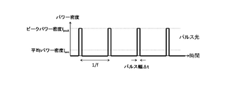
- the case where the laser is a pulse light source is shown in FIG. 7A.
- the average power density I ave is expressed by the following equation (2), where P ave is the average laser power of the laser.
- the peak power density I peak is expressed by the following equation (3), where f is the laser repetition frequency and ⁇ t is the pulse width.
- the case where the laser is a continuous light source is shown in FIG. 7B. Since the laser power is constant over time, the power density of the laser is also constant over time. In order to match the term with the case of the pulse light source, this is hereinafter referred to as the average power density.
- the mechanism of destruction can differ depending on whether the laser is a pulse light source or a continuous light source. Even with a pulsed light source, the mechanism of destruction may differ if the pulse repetition frequency and pulse width are different. However, whatever the mechanism of destruction, laser power per unit area (ie, peak power density or average power density) is generally known to be an important parameter.
- the size of the mirror needs to be larger than the size of the beam.
- the beam diameter of the laser is increased to reduce the power density for the purpose of preventing damage, the mirror size becomes large.
- the load on the motor increases, making it impossible to operate the mirror at high frequencies.
- the KTN optical deflector Since the magnitude of the electric field is the voltage divided by the distance between the electrodes, there is a problem that as the distance between the electrodes increases, the voltage required to generate the electric field required for deflection increases. For this reason, when the KTN optical deflector is operated with a practical voltage of several hundred volts, it is not possible to obtain a large distance between the electrodes, and a large laser power such as material processing by a laser or rust removal by a laser is generated. In the required applications, it could cause damage.
- the present invention has been made to solve the above problems, and an object of the present invention is to provide an electro-optical device in which an electro-optical crystal is not damaged when a laser beam is input.
- the electro-optical device has an incident surface and an exit surface, and is composed of an electro-optical crystal in which incident light is incident on the incident surface at a sharp incident angle to generate an electro-optical effect.
- the axis of rotation of the incident angle is parallel to the direction of the electric field due to the application of voltage, the incident light has the power to cause destruction of the electro-optical crystal below the predetermined incident angle, and the incident light is of the electro-optical crystal. It is incident on the incident surface at an incident angle larger than the incident angle at which fracture occurs.
- the incident light is incident on the incident surface at an incident angle larger than the incident angle at which the electro-optical crystal is destroyed. Therefore, when the laser light is input, the incident light is incident on the incident surface. Damage to the electro-optical crystal can be prevented.
- FIG. 1 is a configuration diagram for explaining a method of investigating the laser light resistance of an electro-optical crystal.
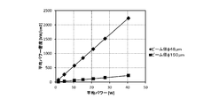
- FIG. 2A is a characteristic diagram showing a calculated value of the average power dependence of an incident light laser having an average power density.
- FIG. 2B is a characteristic diagram showing a calculated value of the average power dependence of the incident light laser having a peak power density.
- FIG. 3 is a configuration diagram showing a configuration of an electro-optic device according to an embodiment of the present invention.
- FIG. 1 is a configuration diagram for explaining a method of investigating the laser light resistance of an electro-optical crystal.
- FIG. 2A is a characteristic diagram showing a calculated value of the average power dependence of an incident light laser having an average power density.
- FIG. 2B is a
- FIG. 5 is a characteristic diagram showing the incident angle ⁇ dependence of the minimum value Wmin of the width of the electro-optical crystal 301.
- FIG. 6 is a configuration diagram showing the configuration of another electro-optical device according to the embodiment of the present invention.
- FIG. 7A is a characteristic diagram showing the time change of the power density when the laser is a pulse light source.
- FIG. 7B is a characteristic diagram showing the time change of the power density when the laser is a continuous light source.
- the results of investigating the laser light resistance of electro-optical crystals will be explained.
- an optical deflector configured by using a KTN crystal (KTN crystal) as an electro-optical crystal
- the experiment for investigation will be described with reference to FIG.
- the first electrode 102 and the second electrode 103 are formed on two surfaces (3.2 mm ⁇ 4 mm) of a rectangular parallelepiped KTN crystal 101 having a size of 3.2 mm ⁇ 4 mm ⁇ 1.2 mm.
- the electro-optical device is an optical deflector
- the first electrode 102 and the second electrode 103 are made of an electrode material in which electrons are injected into an electro-optical crystal by applying a DC voltage.
- an electrode material for example, titanium can be used. These electrodes are formed by thin film deposition. Further, the temperature of the KTN crystal 101 on which the first electrode 102 and the second electrode 103 were formed was controlled to a constant temperature so that the capacitance was 1.47 nF (relative permittivity 15,565). A Perche element and a thermistor were used to control this temperature.
- An optical pulse from a Yb fiber laser light source (wavelength 1.055 to 1.070 ⁇ m, pulse repetition frequency 50 kHz, pulse width 180 ns) that oscillates in multiple modes is sent to the incident surface (3.2 mm ⁇ 1.2 mm) of the KTN crystal 101. It was incident vertically.
- An antireflection film is formed on the incident surface by coating.
- the incident light was deflected by applying a wave voltage (frequency 1 kHz, voltage amplitude 300 V) between the first electrode 102 and the second electrode 103.
- the beam diameter is set to 48 ⁇ m on the incident surface of the KTN crystal 101, and the average power of the light source is 1.44 W, 4.78 W, 10.41 W, 15.2 W, 20.9 W, 27.5 W, 40.5 W. I raised it.
- Figure 2A shows the calculated value of the average power dependence of the incident light laser with the average power density. Further, the calculated value of the average power dependence of the incident light laser having a peak power density is shown in FIG. 2B. Equations (1), (2), and (3) were used to calculate the calculated values. When two light deflector samples were tested, one light deflector sample damaged the KTN crystal 101 when exposed to 40.5 W of light, but the other did not.
- the beam diameter is set to 150 ⁇ m on the incident surface of the KTN crystal 101, and the average power of the light source is 1.44 W, 4.78 W, 10.41 W, 15.2 W, 20.9 W, 27.5 W, 40. I raised it to .5W.
- the average power of the light source is 1.44 W, 4.78 W, 10.41 W, 15.2 W, 20.9 W, 27.5 W, 40. I raised it to .5W.
- a voltage was applied in a state where the temperature was lowered and controlled to a constant temperature so that the capacitance of the KTN crystal 101 was 1.56 nF (relative permittivity 16,518).
- the beam diameter is set to 150 ⁇ m on the incident surface of the KTN crystal 101, and the average power of the light source is similarly 1.44 W, 4.78 W, 10.41 W, 15.2 W, 20.9 W, 27.5 W, 40. I raised it to 5W. When four light deflector samples were tested, no damage to KTN crystal 101 was found in any of them.
- the power density of the light transmitted through the KTN crystal can be set to be less than a certain threshold value (the power density of the limit light that is incident on the incident surface at an incident angle of 0 and causes destruction of the electro-optical crystal). , It is important to prevent damage to KTN crystals.
- the threshold value of the power density of light that causes damage can be freely determined by the user.
- an optical deflector using a plurality of KTN crystals is prepared, measurement conditions such as applied voltage and dielectric constant are adjusted, the power density at which the KTN crystal is broken is recorded, and the average value and standard deviation are used.
- the power density threshold described above can be determined. Further, the lowest value of the destroyed power density can be adopted as the above-mentioned threshold value of the power density.
- This electro-optical device includes an electro-optical crystal 301, a first electrode 302, and a second electrode 303.
- a voltage application mechanism for applying a voltage to the electro-optical crystal 301 by the first electrode 302 and the second electrode 303, a light source, and the like are omitted.
- the electro-optical crystal 301 is controlled by using a temperature measuring element such as a thermistor and a Perche element so that the temperature does not change with time.
- the electro-optical crystal 301 has an electro-optical effect, has an incident surface 311 and an exit surface 312, and incident light is incident on the incident surface 311 at an acute angle.
- the electro-optical device is an optical deflector
- the electro-optical crystal 301 deflects the incident light incident on the incident surface 311 at an acute angle in the direction of the electric field to which the voltage is applied.
- the electro-optical crystal 301 is a KTN [KTa 1- ⁇ Nb ⁇ O 3 (0 ⁇ ⁇ 1)] crystal or a lithium-added KLTN [K 1- ⁇ Li ⁇ Ta 1- ⁇ Nb ⁇ O 3 (0 ⁇ 1)]. It can be composed of any of ⁇ ⁇ 1,0 ⁇ ⁇ 1)] crystals.
- the rotation axis of the incident angle of the incident light described above is parallel to the electric field direction. Further, the incident light has a power that causes destruction of the electro-optical crystal 301 below a predetermined incident angle, and the incident light is on the incident surface 311 at an incident angle larger than the incident angle at which the electro-optical crystal 301 is destroyed. Be incident.
- the electro-optical crystal 301 is, for example, a rectangular parallelepiped.
- the side lengths of the rectangular parallelepiped electro-optical crystal 301 are length L, width W, and thickness H.
- a voltage is applied in the direction of the thickness H.
- Light of power P having a beam diameter (diameter) d is incident on the incident surface 311 having a width W and a thickness H of the electro-optical crystal 301.
- a non-reflective film is formed on the incident surface 311.
- ⁇ be the incident angle of the light described above.
- the rotation axis of the incident angle ⁇ is parallel to the x-axis, that is, parallel to the applied voltage direction.
- the length (diameter of light) of the incident surface 311 on the plane parallel to the yz plane of the region irradiated with light is d / cos ⁇ .
- the diameter of the light propagating in the electro-optical crystal 301 is dcos ⁇ / cos ⁇ .
- the light propagating in the electro-optical crystal 301 is refracted on the exit surface 312 according to Snell's law and output as light having a beam diameter d.
- the beam shape of the incident light is a circle having a beam diameter (diameter) of d has been described, but regardless of the shape, the power density of the light propagating in the electro-optical crystal can be determined. Can be reduced.
- the electro-optical crystal does not have to be a rectangular parallelepiped.
- the electro-optical crystal 601 has an incident surface 611 and an exit surface 612 parallel to each other, and can be a structure having a parallelogram cross section on the yz surface.
- the entrance surface 611 and the exit surface 612 can be an area in which the light beam can be accommodated.
- the electro-optical crystal 601 can be composed of only a portion through which light propagates. By doing so, the volume of the electro-optical crystal 601 can be made smaller.
- the emitting surface does not have to be parallel to the incident surface, and it is sufficient that the propagating light can be emitted from the emitting surface.
- the exit surface may be perpendicular to the traveling direction of the light of the electro-optical crystal, or may be slightly deviated from the vertical.
- the first electrode and the second electrode are made of an electrode material that blocks the injection of electrons into the electro-optical crystal by applying a DC voltage.
- an electrode material for example, platinum can be used.
- the electro-optic device is an optical phase modulator, the incident light is not deflected in the x-axis direction.
- the incident light is incident on the incident surface at an incident angle larger than the incident angle at which the electro-optical crystal is destroyed. , It becomes possible to prevent damage to the electro-optical crystal.
- Electro-optic crystal 302 ... 1st electrode, 303 ... 2nd electrode, 311 ... Incident surface, 312 ... Emission surface.
Landscapes
- Physics & Mathematics (AREA)
- Nonlinear Science (AREA)
- General Physics & Mathematics (AREA)
- Optics & Photonics (AREA)
- Chemical & Material Sciences (AREA)
- Engineering & Computer Science (AREA)
- Ceramic Engineering (AREA)
- Crystallography & Structural Chemistry (AREA)
- Optical Modulation, Optical Deflection, Nonlinear Optics, Optical Demodulation, Optical Logic Elements (AREA)
Priority Applications (3)
| Application Number | Priority Date | Filing Date | Title |
|---|---|---|---|
| US17/918,721 US12265311B2 (en) | 2020-04-16 | 2020-04-16 | Electro-optical device |
| JP2022515151A JP7485015B2 (ja) | 2020-04-16 | 2020-04-16 | 電気光学装置 |
| PCT/JP2020/016788 WO2021210145A1 (ja) | 2020-04-16 | 2020-04-16 | 電気光学装置 |
Applications Claiming Priority (1)
| Application Number | Priority Date | Filing Date | Title |
|---|---|---|---|
| PCT/JP2020/016788 WO2021210145A1 (ja) | 2020-04-16 | 2020-04-16 | 電気光学装置 |
Publications (1)
| Publication Number | Publication Date |
|---|---|
| WO2021210145A1 true WO2021210145A1 (ja) | 2021-10-21 |
Family
ID=78084175
Family Applications (1)
| Application Number | Title | Priority Date | Filing Date |
|---|---|---|---|
| PCT/JP2020/016788 Ceased WO2021210145A1 (ja) | 2020-04-16 | 2020-04-16 | 電気光学装置 |
Country Status (3)
| Country | Link |
|---|---|
| US (1) | US12265311B2 (https=) |
| JP (1) | JP7485015B2 (https=) |
| WO (1) | WO2021210145A1 (https=) |
Citations (6)
| Publication number | Priority date | Publication date | Assignee | Title |
|---|---|---|---|---|
| JPS63170982A (ja) * | 1987-01-08 | 1988-07-14 | Hamamatsu Photonics Kk | 波長可変レ−ザ装置 |
| JPH1055005A (ja) * | 1996-06-05 | 1998-02-24 | Mitsui Petrochem Ind Ltd | レーザ光発生装置 |
| US20060250677A1 (en) * | 2005-01-12 | 2006-11-09 | Hoffman Hanna J | Methods and systems to enhance multiple wave mixing process |
| JP2015158531A (ja) * | 2014-02-21 | 2015-09-03 | 日本電信電話株式会社 | 電気光学素子 |
| JP2017203847A (ja) * | 2016-05-10 | 2017-11-16 | 日本電信電話株式会社 | 光偏向器 |
| CN109167240A (zh) * | 2018-09-14 | 2019-01-08 | 北京空间机电研究所 | 一种抗激光损伤的固体激光器谐振腔 |
Family Cites Families (3)
| Publication number | Priority date | Publication date | Assignee | Title |
|---|---|---|---|---|
| KR100272196B1 (ko) * | 1996-06-05 | 2000-12-01 | 나까니시 히로유끼 | 레이저 광 발생장치 |
| WO2009017142A1 (ja) * | 2007-07-31 | 2009-02-05 | Nippon Telegraph And Telephone Corporation | 分光器 |
| JP6554070B2 (ja) * | 2016-06-08 | 2019-07-31 | 日本電信電話株式会社 | 波長掃引光源およびその制御方法 |
-
2020
- 2020-04-16 US US17/918,721 patent/US12265311B2/en active Active
- 2020-04-16 JP JP2022515151A patent/JP7485015B2/ja active Active
- 2020-04-16 WO PCT/JP2020/016788 patent/WO2021210145A1/ja not_active Ceased
Patent Citations (6)
| Publication number | Priority date | Publication date | Assignee | Title |
|---|---|---|---|---|
| JPS63170982A (ja) * | 1987-01-08 | 1988-07-14 | Hamamatsu Photonics Kk | 波長可変レ−ザ装置 |
| JPH1055005A (ja) * | 1996-06-05 | 1998-02-24 | Mitsui Petrochem Ind Ltd | レーザ光発生装置 |
| US20060250677A1 (en) * | 2005-01-12 | 2006-11-09 | Hoffman Hanna J | Methods and systems to enhance multiple wave mixing process |
| JP2015158531A (ja) * | 2014-02-21 | 2015-09-03 | 日本電信電話株式会社 | 電気光学素子 |
| JP2017203847A (ja) * | 2016-05-10 | 2017-11-16 | 日本電信電話株式会社 | 光偏向器 |
| CN109167240A (zh) * | 2018-09-14 | 2019-01-08 | 北京空间机电研究所 | 一种抗激光损伤的固体激光器谐振腔 |
Also Published As
| Publication number | Publication date |
|---|---|
| JP7485015B2 (ja) | 2024-05-16 |
| US20230236470A1 (en) | 2023-07-27 |
| JPWO2021210145A1 (https=) | 2021-10-21 |
| US12265311B2 (en) | 2025-04-01 |
Similar Documents
| Publication | Publication Date | Title |
|---|---|---|
| Römer et al. | Electro-optic and acousto-optic laser beam scanners | |
| EP1939665B1 (en) | Laser microscope and control method for the same | |
| JP2013140328A (ja) | 光学装置、光偏向装置及び光変調装置 | |
| WO2006137408A1 (ja) | 電気光学素子 | |
| JP5991914B2 (ja) | ビームスキャナおよび偏向光源 | |
| JPH09146128A (ja) | 電気光学素子 | |
| EP0878881A1 (en) | Optical device | |
| EP0805531B1 (en) | Wavelength tunable laser | |
| WO2021210145A1 (ja) | 電気光学装置 | |
| EP0439631B1 (en) | Optical deflector | |
| US7976717B2 (en) | Method of forming polarization reversal area, apparatus thereof and device using it | |
| JP2015031929A (ja) | 光偏向装置 | |
| JP2009012011A (ja) | レーザ加工装置 | |
| JP5006748B2 (ja) | 電気光学素子及び光ビーム偏向器 | |
| JPH10307307A (ja) | 光学偏向器 | |
| JP7485091B2 (ja) | 波長可変光フィルタ | |
| US6204952B1 (en) | Bragg modulator | |
| JP2603086B2 (ja) | 光導波路素子 | |
| Fefelov et al. | Application of optomechanical modulators for IR solid state laser schemes | |
| JP6039485B2 (ja) | 光偏向器およびその駆動方法 | |
| JPH11271816A (ja) | レーザ光制御装置及び方法 | |
| US12504666B2 (en) | Optical deflector | |
| US5706370A (en) | Optical deflection scanning device | |
| JP7548325B2 (ja) | 光偏向器および光偏向器の制御条件の決定方法 | |
| JP6487835B2 (ja) | 光偏向器およびその制御方法 |
Legal Events
| Date | Code | Title | Description |
|---|---|---|---|
| 121 | Ep: the epo has been informed by wipo that ep was designated in this application |
Ref document number: 20931424 Country of ref document: EP Kind code of ref document: A1 |
|
| ENP | Entry into the national phase |
Ref document number: 2022515151 Country of ref document: JP Kind code of ref document: A |
|
| NENP | Non-entry into the national phase |
Ref country code: DE |
|
| 122 | Ep: pct application non-entry in european phase |
Ref document number: 20931424 Country of ref document: EP Kind code of ref document: A1 |
|
| WWG | Wipo information: grant in national office |
Ref document number: 17918721 Country of ref document: US |