WO2021200569A1 - センサデバイスおよびその製造方法 - Google Patents
センサデバイスおよびその製造方法 Download PDFInfo
- Publication number
- WO2021200569A1 WO2021200569A1 PCT/JP2021/012619 JP2021012619W WO2021200569A1 WO 2021200569 A1 WO2021200569 A1 WO 2021200569A1 JP 2021012619 W JP2021012619 W JP 2021012619W WO 2021200569 A1 WO2021200569 A1 WO 2021200569A1
- Authority
- WO
- WIPO (PCT)
- Prior art keywords
- layer
- sensor device
- vibrator
- electrode
- drain electrode
- Prior art date
- Legal status (The legal status is an assumption and is not a legal conclusion. Google has not performed a legal analysis and makes no representation as to the accuracy of the status listed.)
- Ceased
Links
Images


Classifications
-
- G—PHYSICS
- G01—MEASURING; TESTING
- G01N—INVESTIGATING OR ANALYSING MATERIALS BY DETERMINING THEIR CHEMICAL OR PHYSICAL PROPERTIES
- G01N27/00—Investigating or analysing materials by the use of electric, electrochemical, or magnetic means
-
- G—PHYSICS
- G01—MEASURING; TESTING
- G01N—INVESTIGATING OR ANALYSING MATERIALS BY DETERMINING THEIR CHEMICAL OR PHYSICAL PROPERTIES
- G01N5/00—Analysing materials by weighing, e.g. weighing small particles separated from a gas or liquid
- G01N5/02—Analysing materials by weighing, e.g. weighing small particles separated from a gas or liquid by absorbing or adsorbing components of a material and determining change of weight of the adsorbent, e.g. determining moisture content
Definitions
- the present invention relates to a sensor device and a method for manufacturing the same.
- the gas sensor described in Non-Patent Document 1 has a substrate, a gate electrode, a drain electrode and a source electrode arranged on the substrate, and a graphene layer.
- This gas sensor has a structure that vibratesly supports the graphene layer between the drain electrode and the source electrode, and detects the gas component based on the amount of change in the resonance frequency of the graphene layer due to the adsorption of gas.
- the vibrator of the gas sensor In order to perform gas detection with higher sensitivity, it is necessary for the vibrator of the gas sensor to detect the change in resonance frequency due to gas adsorption with high accuracy. This means that the Q value of the oscillator needs to be high. Furthermore, in order to specify the vibration mode required for gas detection, it is required that the vibrator does not generate a natural vibration mode that interferes with the desired vibration mode.
- an object of the present invention is to provide a sensor device capable of increasing the detection sensitivity of gas and a method for manufacturing the same.
- the sensor device includes a substrate, an insulating film, a gate electrode, a source electrode, a drain electrode, and a vibrator.
- the insulating film is formed on the substrate.
- the gate electrode is arranged on the insulating film.
- the source electrode has a first conductor layer and a second conductor layer provided on the first conductor layer, and is arranged on the insulating film.
- the drain electrode has a third conductor layer and a fourth conductor layer provided on the third conductor layer, and is arranged on the insulating film.
- the vibrator includes a first end portion sandwiched between the first and second conductor layers, a second end portion sandwiched between the third and fourth conductor layers, and a vibrating portion facing the gate electrode. Has.
- the above oscillator may include a graphene layer.
- the vibrator may further include a sensitive film formed on the graphene layer.
- the sensitive membrane may be a porous membrane.
- the porous membrane may be a carbon-based material.
- the first to fourth conductor layers may be made of the same type of metal material.
- the source electrode is arranged between the first and second conductor layers and further has an adhesion layer in close contact with the vibrator, and the drain electrode is arranged between the third and fourth conductor layers.
- An adhesion layer that is in close contact with the vibrator may be further provided.
- the gate electrode may be arranged between the substrate and the vibrator.
- a method for manufacturing a sensor device includes forming a lower electrode layer on a substrate.
- a graphene layer is formed on the lower electrode layer.
- An upper electrode layer is formed on the graphene layer.
- the gas detection sensitivity can be increased.
- FIG. 1 is a schematic diagram showing the configuration of a gas determination system.
- FIG. 2 is a schematic view showing the configuration of the sensor device 10 that constitutes a part of the gas determination system.
- the gas determination system 1 includes a sensor device 2, an information processing device 4, a display device 5, and a storage unit 6.
- the sensor device 2 includes a storage chamber 20, a sensor device 10, a UV (ultraviolet) light source 23, and a heating unit 26.
- the storage chamber 20 houses the sensor device 10, the UV light source 23, and the heating unit 26.
- the accommodation chamber 20 has an intake port 21 for sucking gas from the outside and an exhaust port 22 for exhausting the gas introduced into the accommodation chamber 20 from the accommodation chamber 20 to the outside.
- the intake port 21 is provided with a valve 24 for adjusting the inflow of gas into the accommodation chamber 20, and the exhaust port 22 is provided with a valve 25 for adjusting the outflow of gas in the accommodation chamber 20 to the outside.
- the UV light source 23 emits ultraviolet rays (UV) to irradiate the sensor device 10. Cleaning of the vibrator 16 is performed by irradiating the vibrator 16 of the sensor device 10 described later with UV. By performing UV irradiation, the gas is efficiently adsorbed on the vibrator 16. This is because O 2 , H 2 O, etc. are removed from the surface of the vibrator 16 by UV irradiation (cleaning effect), and between adsorption of gas molecules on the surface of the vibrator 16 and photoexcitation desorption.
- UV ultraviolet rays
- the heating unit 26 is, for example, a heater and heats the sensor device 10. By heating the sensor device 10 by the heating unit 26, the gas adsorption effect of the vibrator 16 can be obtained.
- the sensor device 10 includes a substrate 11, an insulating film 12, a gate electrode 13, a source electrode 14, a drain electrode 15, and a vibrator 16.
- the substrate 11 is typically a silicon substrate, but may be a semiconductor substrate or a glass substrate other than silicon.
- the insulating film 12 is formed on the substrate 11.
- the insulating film 12 is typically a silicon oxide film, and when the substrate 11 is a silicon substrate, it is a thermal oxide film formed on the surface thereof.
- the gate electrode 13, the source electrode 14, and the drain electrode 15 are formed on the insulating film 12.
- the gate electrode 13 is arranged between the source electrode 14 and the drain electrode 15.
- the gate electrode 13, the source electrode 14, and the drain electrode 15 are typically metal films, and in this embodiment, they are composed of a laminated film of chromium (Cr) and gold (Au).
- the vibrator 16 is arranged between the source electrode 14 and the drain electrode 15 so as to face the gate electrode 13.
- the vibrator 16 is arranged with a gap so as not to come into contact with the gate electrode 13.
- the vibrator 16 is made of a conductive material, and in this embodiment, is made of a graphene layer.
- the graphene layer is composed of a single layer film, but may be a multilayer film.
- the vibrator 16 may be made of another conductive material such as a metal film or a silicon thin film.
- the vibrator 16 is composed of a laminated film of a graphene layer 160 and a sensitive film 17 formed on the surface thereof.
- the sensitive film 17 is made of, for example, a material capable of adsorbing the gas to be detected.
- the material constituting the sensitive film 17 can be arbitrarily selected depending on the type of gas to be detected, and typically, an organic polymer film (organic polymer film, organic low molecular weight film), an organic dye film, an inorganic film, or the like is used. be able to.
- the sensitive film 17 may be a porous film.
- the porous film is formed by decorating the surface of the graphene layer 160 with activated carbon.
- the material constituting the porous film is not limited to activated carbon, and may be more porous than the graphene layer 160, and may have conductive properties similar to the graphene layer 160.
- the porous membrane is made of the same carbon-based material as the graphene layer 160.
- a carbon-based material is a substance containing carbon as a main component.
- the porous membrane Since the porous membrane has a function of promoting gas adsorption, it has a large adsorption surface area due to its porosity, and since it has many dangling bonds, it can efficiently adsorb gas. Since the porous film has conductive properties, the adsorption surface area is larger and the surface has many dangling bonds as compared with the case where a film having no conductive properties is provided on the graphene layer 160 as an adsorption film. , Gas molecule adsorption is promoted.
- the thickness of the porous film is not particularly limited, and may be the same as the thickness of the graphene layer 160, or may be thinner or thicker than the thickness of the graphene layer 160.
- the graphene layer 160 has a thickness of 1 nm and the porous film has a thickness of 1 nm.
- the porous film is formed so as to cover the entire surface of the graphene layer 160, but is not limited to this, and may be formed so as to cover at least a part of the surface of the graphene layer 160.
- the information processing device 4 includes an acquisition unit 41, a determination unit 42, an output unit 43, and a control unit 44.
- the information processing device 4 controls the drive of the sensor device 10, determines the detection component of the gas based on the amount of change in the resonance frequency of the vibrator 16, and outputs the determination result.
- the control unit 44 resonates the vibrator 16 by inputting a high frequency signal of a predetermined frequency between the gate electrode 13 and the source electrode 14 of the sensor device 10.
- the acquisition unit 41 acquires a high-frequency signal (drain current) corresponding to the resonance frequency of the vibrator 16 from the drain electrode 15 and converts it into a change in the resonance frequency of the vibrator 16 based on the drain current.
- the determination unit 42 determines the type or concentration of the gas based on the plurality of resonance frequency changes acquired by the acquisition unit 41 with reference to the resonance frequency information stored in the storage unit 6.
- the output unit 43 outputs the determination result by the determination unit 42 to the display device 5.
- the mass of the vibrator 16 changes due to the adsorption of the gas on the vibrator 16, and the resonance frequency of the vibrator 16 decreases based on the amount of change in the mass. ..
- the mass of the vibrator 16 before gas adsorption is m
- the amount of change in the mass of the vibrator 16 due to gas adsorption is ⁇ m
- the resonance frequency of the vibrator 16 is f0
- the amount of change ⁇ f in the resonance frequency of the vibrator 16 is expressed by the formula. Calculated in (1).
- ⁇ f ⁇ m ⁇ f0 / (2 ⁇ m) ⁇ ⁇ ⁇ (1)
- the vibrator 16 is composed of carbon, which is a light element, and graphene, which has excellent electrical and mechanical properties, the frequency change can be detected with high sensitivity.
- the information processing device 4 acquires resonance frequency information for each of a plurality of different types of gases in advance and stores them in the storage unit 6.
- the determination unit 42 identifies and determines the type of gas detected by the sensor device 10 with reference to the resonance frequency information stored in the storage unit 6.
- the output unit 43 outputs the determination result such as the resonance frequency information acquired by the acquisition unit 41 and the type and concentration of the gas determined by the determination unit 42 to the display device 5.
- the display device 5 has a display unit, and displays the type and concentration of gas output from the information processing device 4 on the display unit. The user can grasp the gas determination result by checking the display unit.
- the storage unit 6 acquires in advance resonance frequency information for each of a plurality of known gases of different types detected by the gas determination system 1 and stores them as reference data.
- the storage unit 6 is composed of a storage device such as an HDD (Hard Disk Drive) or a semiconductor memory.
- the storage unit 6 may be on a cloud server on which the information processing device 4 can communicate, or may be provided in the information processing device 4.
- FIG. 4 is a side sectional view of the sensor device 10.
- the vibrator 16 is arranged between the source electrode 14 and the drain electrode 15 so as to face the gate electrode 13. More specifically, the vibrator 16 has a first end portion 161 supported by the source electrode 14, a second end portion 162 supported by the drain electrode 15, and a vibrating portion 163 facing the gate electrode 13. ..
- the vibrator 16 is arranged with a predetermined gap (for example, 100 nm) in the thickness direction of the substrate 11 with respect to the gate electrode 13 so that the vibrating portion 163 can vibrate.
- the source electrode 14 and the drain electrode 15 have a laminated structure of at least two conductor layers. That is, the source electrode 14 includes a first source electrode layer 141 (first conductor layer) provided on the insulating film 12 and a second source electrode layer 142 (first conductor layer) provided on the first source electrode layer 141. It has two conductor layers). Further, the drain electrode 15 includes a first drain electrode layer 151 (third conductor layer) provided on the insulating film 12 and a second drain electrode layer 152 (third conductor layer) provided on the first drain electrode layer 151. It has 4 conductor layers).
- the first end portion 161 of the vibrator 16 is arranged between the electrode layers 141 and 142 so as to be sandwiched between the first source electrode layer 141 and the second source electrode layer 142.
- the second end portion 162 of the vibrator 16 is arranged between the electrode layers 151 and 152 so as to be sandwiched between the first drain electrode layer 151 and the second drain electrode layer 152.
- the first source electrode layer 141 and the first drain electrode layer 151 are formed to have a thickness larger than that of the gate electrode 13, so that the predetermined gap is formed between the vibrating portion 163 of the vibrator 16 and the gate electrode 13. Will be done.
- both ends of the vibrator 16 are supported so as to be sandwiched between the conductor layers (electrode layers) constituting the source electrode 14 and the drain electrode 15. ,
- the vibrator 16 can be stably held. Therefore, since the vibrator 16 is less likely to come off, deterioration of the sensor device 10 over time can be suppressed and durability can be improved.
- a close contact layer such as chromium (Cr) that is in close contact with the first end portion 161 of the vibrator 16 may be provided between the first source electrode layer 141 and the second source electrode layer 142.
- a close contact layer such as Cr that is in close contact with the second end portion 162 of the vibrator 16 may be provided between the first drain electrode 151 and the second drain electrode 152.
- first source electrode layer 141 and the second source electrode layer 142 are each made of the same type of metal material.
- first drain electrode layer 151 and the second drain electrode layer 152 are each made of the same type of metal material.
- the same kind of metal material means an alloy material having the same main metal material as well as the same metal material.
- FIG. 5 is a side sectional view showing the configuration of the sensor device 110 according to the comparative example.
- the source electrode 114 and the drain electrode 115 are formed on the insulating film 12 of the substrate 11, and the insulating film 12 between the source electrode 114 and the drain electrode 115 has a recess for arranging the gate electrode 13. 120 is formed.
- the vibrator 116 is arranged in the recess 120 so as to face the gate electrode 13, and the upper surfaces of both ends of the vibrator 116 are supported by the lower surfaces of the source electrode 114 and the drain electrode 115, respectively.
- the recess 120 is formed by a wet etching method using the source electrode 114 and the drain electrode 115 as masks. Since wet etching is isotropic etching, the recess 120 is accompanied by under-etching that erodes a part of the interface between the insulating film 12 and the source electrode 114 and the drain electrode 115. As a result, in the source electrode 114 and the drain electrode 115, a region that is not supported by the insulating film 12 that is the base layer is generated in the vicinity of the end portion that supports the vibrator 116.
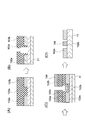
- FIG. 6A and 6 (B) are simulation results for evaluating the vibration mode of the sensor device 110 according to the comparative example.
- FIG. 6A shows the sensor in the primary vibration mode of the device
- FIG. 6B shows the secondary vibration mode thereof.
- the thickness of the source electrode 114 and the drain electrode 115 is 75 nm
- the thickness of the insulating film 12 is 280 nm
- the width of the source electrode 114 and the drain electrode 115 is 3 ⁇ m
- the facing distance L1 between the source electrode 114 and the drain electrode 115 FIG. 5
- the vibrator 116 has two natural frequencies of 19.7 MHz and 20.2 MHz
- the Q value of each is 3080 in the case of 19.7 MHz and 1509 in the case of 20.2 MHz. Met.
- FIGS. 7A and 7B are simulation results for evaluating the vibration mode of the sensor device 10 according to the present embodiment shown in FIG.
- FIG. 7A shows the sensor in the primary vibration mode of the device
- FIG. 7B shows the secondary vibration mode thereof.
- the thickness of the source electrode 14 and the drain electrode 15 is 150 nm (the thickness of each of the first source electrode layer 141, the second source electrode layer 142, the first drain electrode layer 151, and the second drain electrode layer 152 is 75 nm).
- the thickness of the insulating film 12 was 280 nm, the width of the source electrode 14 and the drain electrode 15 was 3 ⁇ m, and the facing distance between the source electrode 14 and the drain electrode 15 (the length of the vibrating portion 163 of the vibrator 16) was 1 ⁇ m.
- the vibrator 16 has two natural frequencies of 26.9 MHz and 77.6 MHz, and the Q value of each is 10087 in the case of 26.9 MHz and 10009 in the case of 77.6 MHz. Met.
- the Q value of the vibrator which is more than 3 times higher than that of the comparative example, was obtained. It is probable that the result in the comparative example is that the vibrator is not sufficiently fixed because the vibrator is formed by the under-etching of the insulating film 12, and the Q value of the vibrator 116 is lowered because the vibration energy is dissipated to the outside. ..
- both ends of the vibrator 16 are sandwiched between the layers constituting the source electrode 14 and the drain electrode 15 and are firmly fixed, so that the energy of vibration is not dissipated to the outside and is high. It is probable that the Q value was obtained.
- the responsiveness of the gas can be significantly improved as compared with the structure of the comparative example.
- the difference between the two natural frequencies was small, and the values were close to each other. This indicates that if one is selected as the primary vibration mode for gas sensing, interference with the other vibration mode is unavoidable. This is brought about by the fact that the source electrode 114 and the drain electrode 115 function as a part of the vibrator 116, thereby forming an undesired vibration mode.
- the difference between the two natural frequencies is large. This means that when one vibration mode is used for gas sensing, the influence of the other vibration mode hardly appears, and the generation of extra vibration mode that can be caused by underetching is suppressed. Shown.
- the insulating film 12 is formed on the substrate 11.
- the first resist resin layer 101a is formed on the substrate 110
- the second resist resin layer 101b is formed on the first resist resin layer 101a.
- MMA methyl methacrylate
- PMMA polymethylmethacrylate
- a resist pattern is formed by exposing and developing the first resist resin layer 101a and the second resist resin layer 101b using electron beam lithography technology or the like.
- an opening pattern in which the pattern width of the second resist resin layer 101b is larger than the pattern width of the first resist resin layer 101a is formed.
- the first metal layer 102a is formed on the surface of the second resist resin layer 101b and inside the opening thereof.
- the first metal layer 102a is patterned (lifted off) by removing the first and second resist resin layers 101a and 101b, and the pattern of the first metal layer 102a is applied to the substrate 11. Form on top.
- the first metal layer 102a may be a single layer or may have a multi-layer structure.
- chromium (Cr) having a thickness of about 10 nm is formed as an adhesion material
- gold (Au) having a thickness of about 130 nm is formed on the chromium (Cr) as an electrode material.
- the film forming method of the first metal layer 102a is not particularly limited, and may be a sputtering method or a vacuum vapor deposition method.
- the first metal layer 102a is formed by the electron beam deposition method.
- the first metal layer 102a corresponds to the first source electrode layer 141 and the first drain electrode layer 151 in the sensor device 10 shown in FIG.
- the third resist resin layer 103a is formed on the substrate 11, and the fourth resist resin layer 103b is formed on the third resist resin layer 103a.
- the third resist resin layer 103a for example, a methyl methacrylate (MMA) film is used
- the fourth resist resin layer 103b for example, a polymethylmethacrylate (PMMA) film is used. Used.
- a resist pattern is formed by exposing and developing the third resist resin layer 103a and the fourth resist resin layer 103b using electron beam lithography technology or the like.
- an opening pattern in which the opening width of the third resist resin layer 103a is larger than the opening width of the fourth resist resin layer 103b is formed.
- a second metal layer 102b is formed on the surface of the fourth resist resin layer 103b and inside the opening thereof, and then the sacrificial layer 104 is formed on the surface of the second metal layer 102b.
- the sacrificial layer 104 is made of, for example, a resist resin.
- the third and fourth resist resin layers 103a and 103b and the second metal layer 102b formed on the fourth resist resin layer 103b are removed.
- the sacrificial layer 104 formed on the second metal layer 102b and the second metal layer 102b is patterned (lifted off), and the pattern of the second metal layer 102b and the sacrificial layer 104 is formed on the substrate 11.
- the second metal layer 102b may be a single layer or may have a multi-layer structure.
- chromium (Cr) having a thickness of about 10 nm is formed as an adhesion material
- gold (Au) having a thickness of about 30 nm is formed on the chromium (Cr) as an electrode material.
- the film forming method of the second metal layer 102b is not particularly limited, and may be a sputtering method or a vacuum vapor deposition method. In this embodiment, the second metal layer 102b is formed by the electron beam deposition method.
- the second metal layer 102b corresponds to the gate electrode 13 in the sensor device 10 shown in FIG. Further, the laminated thickness of the second metal layer 102b and the sacrificial layer 104 is typically the same as the thickness of the first metal layer 102a. In the present embodiment, since the opening width of the third resist resin layer 103a is larger than the opening width of the fourth resist resin layer 103b, the second metal layer 102b is less likely to come into contact with the side surface of the opening of the third resist resin layer 103a. As a result, the patterning accuracy of the second metal layer 102b at the time of lift-off can be improved.
- the laminate of the graphene layer 105 and the protective layer 106 is transferred to the first metal layer 102a.
- the protective layer 106 is made of, for example, a resist resin.
- the protective layer 106 is removed.
- the graphene layer 105 corresponds to the vibrator 16 in the sensor device 10 of FIG.
- the third metal layer 102c is formed on the first metal layer 102a.
- the third metal layer 102c is formed, and then the resist pattern is removed to form the third metal layer 102c. Patterning (lift off).
- the third metal layer 102c faces the first metal layer 102a with the graphene layer 105 interposed therebetween.
- the shape of the third metal layer 102c is not particularly limited, and in the present embodiment, the third metal layer 102c is formed in an area smaller than that of the first metal layer 102a.
- the third metal layer 102c corresponds to the second source electrode 142 and the second drain electrode 152 in the sensor device 10 of FIG.
- the fifth resist resin layer 107a is formed on the graphene layer 105 and the third metal layer 102c, and the sixth resist resin layer 107b is formed on the fifth resist resin layer 107a.
- the fifth resist resin layer 107a for example, a polymethylmethacrylate (PMMA) film is used
- the sixth resist resin layer 107b for example, an AR-N film is used.
- a resist pattern is formed by exposing and developing only the sixth resist resin layer 107b using electron beam lithography technology or the like.
- the fifth resist resin layer 107a and the graphene layer 105 that are not coated with the sixth resist resin layer 107b are removed by dry etching.
- dry etching method for example, O 2 plasma is used.
- FIG. 11B the fifth and sixth resist resin layers 107a and 107b are removed, and as shown in FIG. 11C, the sacrificial layer 104 is removed.
- the sensor device 10 having a bottom gate structure in which the gate electrode 13 is arranged between the insulating film 12 of the substrate 11 and the vibrator 16 has been described as an example, but the present invention is not limited to this.
- the present invention is also applicable to a sensor device having a top gate structure in which the electrodes are located directly above the vibrator.
Landscapes
- Chemical & Material Sciences (AREA)
- General Health & Medical Sciences (AREA)
- Life Sciences & Earth Sciences (AREA)
- Health & Medical Sciences (AREA)
- Analytical Chemistry (AREA)
- Biochemistry (AREA)
- Physics & Mathematics (AREA)
- General Physics & Mathematics (AREA)
- Immunology (AREA)
- Pathology (AREA)
- Chemical Kinetics & Catalysis (AREA)
- Electrochemistry (AREA)
- Investigating Or Analyzing Materials By The Use Of Electric Means (AREA)
Priority Applications (1)
| Application Number | Priority Date | Filing Date | Title |
|---|---|---|---|
| JP2022512078A JP7717052B2 (ja) | 2020-03-31 | 2021-03-25 | センサデバイスおよびその製造方法 |
Applications Claiming Priority (2)
| Application Number | Priority Date | Filing Date | Title |
|---|---|---|---|
| JP2020063788 | 2020-03-31 | ||
| JP2020-063788 | 2020-03-31 |
Publications (1)
| Publication Number | Publication Date |
|---|---|
| WO2021200569A1 true WO2021200569A1 (ja) | 2021-10-07 |
Family
ID=77928833
Family Applications (1)
| Application Number | Title | Priority Date | Filing Date |
|---|---|---|---|
| PCT/JP2021/012619 Ceased WO2021200569A1 (ja) | 2020-03-31 | 2021-03-25 | センサデバイスおよびその製造方法 |
Country Status (2)
| Country | Link |
|---|---|
| JP (1) | JP7717052B2 (https=) |
| WO (1) | WO2021200569A1 (https=) |
Citations (5)
| Publication number | Priority date | Publication date | Assignee | Title |
|---|---|---|---|---|
| US20120206012A1 (en) * | 2008-12-01 | 2012-08-16 | The Trustees Of Columbia University In The City Of New York | Electromechanical devices and methods for fabrication of the same |
| CN102862949A (zh) * | 2012-09-07 | 2013-01-09 | 清华大学 | 基于倒置工艺的双臂梁mems器件及其形成方法 |
| KR20130134538A (ko) * | 2012-05-31 | 2013-12-10 | 연세대학교 산학협력단 | 성능조절이 가능한 초 고감도 그라핀 센서 및 그 제조방법 |
| JP2015019142A (ja) * | 2013-07-09 | 2015-01-29 | 日本電波工業株式会社 | 圧電デバイス及び圧電デバイスの製造方法 |
| WO2018180793A1 (ja) * | 2017-03-28 | 2018-10-04 | 富士フイルム株式会社 | ガス検知素子及びその製造方法 |
Family Cites Families (2)
| Publication number | Priority date | Publication date | Assignee | Title |
|---|---|---|---|---|
| JPS61100627A (ja) * | 1984-10-24 | 1986-05-19 | Yokogawa Hokushin Electric Corp | 振動式歪センサ |
| JP5618374B2 (ja) | 2011-06-24 | 2014-11-05 | 日本電信電話株式会社 | 機械共振器 |
-
2021
- 2021-03-25 JP JP2022512078A patent/JP7717052B2/ja active Active
- 2021-03-25 WO PCT/JP2021/012619 patent/WO2021200569A1/ja not_active Ceased
Patent Citations (5)
| Publication number | Priority date | Publication date | Assignee | Title |
|---|---|---|---|---|
| US20120206012A1 (en) * | 2008-12-01 | 2012-08-16 | The Trustees Of Columbia University In The City Of New York | Electromechanical devices and methods for fabrication of the same |
| KR20130134538A (ko) * | 2012-05-31 | 2013-12-10 | 연세대학교 산학협력단 | 성능조절이 가능한 초 고감도 그라핀 센서 및 그 제조방법 |
| CN102862949A (zh) * | 2012-09-07 | 2013-01-09 | 清华大学 | 基于倒置工艺的双臂梁mems器件及其形成方法 |
| JP2015019142A (ja) * | 2013-07-09 | 2015-01-29 | 日本電波工業株式会社 | 圧電デバイス及び圧電デバイスの製造方法 |
| WO2018180793A1 (ja) * | 2017-03-28 | 2018-10-04 | 富士フイルム株式会社 | ガス検知素子及びその製造方法 |
Non-Patent Citations (1)
| Title |
|---|
| ZHU ALEXANDER Y ET AL.: "Optoelectromechanical Multimodal Biosensor with Graphene active Region", NANO LETTERS, vol. 14, 2014, pages 5641 - 5649, XP055792254, DOI: 10.1021/nl502279c * |
Also Published As
| Publication number | Publication date |
|---|---|
| JP7717052B2 (ja) | 2025-08-01 |
| JPWO2021200569A1 (https=) | 2021-10-07 |
Similar Documents
| Publication | Publication Date | Title |
|---|---|---|
| Mistry et al. | Highly sensitive self-actuated zinc oxide resonant microcantilever humidity sensor | |
| KR101245296B1 (ko) | 전기 응답 디바이스 | |
| US20150065364A1 (en) | Self-sensing array of microcantilevers for chemical detection | |
| JP3955323B2 (ja) | 選択作用性透過面を有するガス流路及びその透過面の製法 | |
| Chen et al. | Biosensor for human IgE detection using shear-mode FBAR devices | |
| US9927401B2 (en) | Gravimetric gas sensor having a lowered detection limit | |
| CN113454449A (zh) | 具有作为声音检测器的振动结构的光声光谱仪 | |
| Wu et al. | Transformation from Helmholtz to membrane resonance by electro‐adhesive zip of a double‐layer micro‐slit acoustic absorber | |
| JP2018092144A (ja) | フォトマスク及びその製造方法 | |
| Wasisto et al. | Vertical silicon nanowire array‐patterned microcantilever resonators for enhanced detection of cigarette smoke aerosols | |
| JP2010020820A (ja) | 磁気ディスク装置、ガスセンサ、及びその製造方法 | |
| Hallam et al. | Large area suspended graphene for nano‐mechanical devices | |
| WO2021200569A1 (ja) | センサデバイスおよびその製造方法 | |
| JP6625110B2 (ja) | フォトマスク及びその製造方法 | |
| US20240337956A1 (en) | Apparatus and method for preparing and cleaning a component | |
| KR101608817B1 (ko) | 교차지 전극 구조를 갖는 용량성 바이오 센서용 전극 구조체, 상기 전극 구조체의 제조방법 및 상기 전극 구조체를 포함하는 용량성 바이오 센서 | |
| JP4497202B2 (ja) | マイクロフラップ型ナノ・マイクロ機械素子、及びその製造方法 | |
| CN101795962A (zh) | 纳米机电结构和它的制造方法 | |
| KR20160081256A (ko) | 표면 탄성파를 이용한 그래핀 가스센서 | |
| KR100845717B1 (ko) | 초소형 마이크로 브리지 질량 센서를 이용한 인체바이오마커 센서 및 모듈 | |
| Saya et al. | Piezoelectric nanoelectromechanical systems integrating microcontact printed lead zirconate titanate films | |
| JP7768878B2 (ja) | センサデバイス、センサデバイスの製造方法およびガス判定システム | |
| JP4535502B2 (ja) | 物質検出素子 | |
| Darbari et al. | Branched carbon nanotubes to realize a novel capacitive sensor and actuator device | |
| Hajjam et al. | MEMS resonant sensors for detection of gasoline vapor |
Legal Events
| Date | Code | Title | Description |
|---|---|---|---|
| 121 | Ep: the epo has been informed by wipo that ep was designated in this application |
Ref document number: 21779867 Country of ref document: EP Kind code of ref document: A1 |
|
| ENP | Entry into the national phase |
Ref document number: 2022512078 Country of ref document: JP Kind code of ref document: A |
|
| NENP | Non-entry into the national phase |
Ref country code: DE |
|
| 122 | Ep: pct application non-entry in european phase |
Ref document number: 21779867 Country of ref document: EP Kind code of ref document: A1 |