WO2021200523A1 - 撮像装置及び撮像方法 - Google Patents
撮像装置及び撮像方法 Download PDFInfo
- Publication number
- WO2021200523A1 WO2021200523A1 PCT/JP2021/012452 JP2021012452W WO2021200523A1 WO 2021200523 A1 WO2021200523 A1 WO 2021200523A1 JP 2021012452 W JP2021012452 W JP 2021012452W WO 2021200523 A1 WO2021200523 A1 WO 2021200523A1
- Authority
- WO
- WIPO (PCT)
- Prior art keywords
- detection
- flicker
- detection signal
- unit
- signal
- Prior art date
- Legal status (The legal status is an assumption and is not a legal conclusion. Google has not performed a legal analysis and makes no representation as to the accuracy of the status listed.)
- Ceased
Links
Images















Classifications
-
- H—ELECTRICITY
- H04—ELECTRIC COMMUNICATION TECHNIQUE
- H04N—PICTORIAL COMMUNICATION, e.g. TELEVISION
- H04N25/00—Circuitry of solid-state image sensors [SSIS]; Control thereof
- H04N25/47—Image sensors with pixel address output; Event-driven image sensors; Selection of pixels to be read out based on image data
-
- G—PHYSICS
- G01—MEASURING; TESTING
- G01B—MEASURING LENGTH, THICKNESS OR SIMILAR LINEAR DIMENSIONS; MEASURING ANGLES; MEASURING AREAS; MEASURING IRREGULARITIES OF SURFACES OR CONTOURS
- G01B11/00—Measuring arrangements characterised by the use of optical techniques
-
- H—ELECTRICITY
- H04—ELECTRIC COMMUNICATION TECHNIQUE
- H04N—PICTORIAL COMMUNICATION, e.g. TELEVISION
- H04N23/00—Cameras or camera modules comprising electronic image sensors; Control thereof
- H04N23/70—Circuitry for compensating brightness variation in the scene
- H04N23/745—Detection of flicker frequency or suppression of flicker wherein the flicker is caused by illumination, e.g. due to fluorescent tube illumination or pulsed LED illumination
-
- H—ELECTRICITY
- H04—ELECTRIC COMMUNICATION TECHNIQUE
- H04N—PICTORIAL COMMUNICATION, e.g. TELEVISION
- H04N25/00—Circuitry of solid-state image sensors [SSIS]; Control thereof
- H04N25/60—Noise processing, e.g. detecting, correcting, reducing or removing noise
- H04N25/65—Noise processing, e.g. detecting, correcting, reducing or removing noise applied to reset noise, e.g. KTC noise related to CMOS structures by techniques other than CDS
-
- H—ELECTRICITY
- H04—ELECTRIC COMMUNICATION TECHNIQUE
- H04N—PICTORIAL COMMUNICATION, e.g. TELEVISION
- H04N25/00—Circuitry of solid-state image sensors [SSIS]; Control thereof
- H04N25/70—SSIS architectures; Circuits associated therewith
- H04N25/79—Arrangements of circuitry being divided between different or multiple substrates, chips or circuit boards, e.g. stacked image sensors
Definitions
- the present disclosure relates to an imaging device and an imaging method.
- an asynchronous imaging device called DVS (Dynamic Vision Sensor) has been proposed (see, for example, Patent Document 1).
- DVS Dynamic Vision Sensor
- an asynchronous image pickup device can acquire image data at a much higher speed than a general synchronous image pickup device that unnecessarily acquires all image data at a fixed frame rate.
- Lighting fixtures such as fluorescent lamps and LEDs (Light Emitting Devices) change their lighting intensity in synchronization with the frequency of commercial power supplies. This phenomenon is called flicker. Since DVS has excellent sensitivity, it also reacts to changes in brightness due to flicker generated in lighting equipment such as fluorescent lamps and LEDs, and there is a risk of causing an event even in a scene where there is essentially no movement. .. In addition, the power consumption of the DVS increases by generating unnecessary events that are originally necessary.
- the present disclosure provides an imaging device and an imaging method that do not cause unnecessary events.
- a photoelectric conversion unit having a plurality of photoelectric conversion elements, each of which photoelectrically converts incident light to generate an electric signal, and a photoelectric conversion unit.
- a first detection unit that detects a detection signal when the absolute value of the amount of change in the electric signal generated by the plurality of photoelectric conversion elements exceeds a predetermined threshold value.
- a flicker determination unit that determines whether or not the detection signal caused by the flicker of the light source is included in the detection signal detected by the first detection unit. When it is determined that the flicker contains a factor detection signal, a second detection unit that detects a detection signal of a factor other than the flicker from the detection signals detected by the first detection unit.
- An imaging device is provided.
- the first detection unit detects the first detection signal when the absolute value of the amount of change in the direction in which the signal level of the electric signal increases exceeds the first threshold value, and at the same time, the signal level of the electric signal decreases.
- the second detection signal is detected when the absolute value of the amount of change in direction exceeds the second threshold value, and
- the flicker determination unit includes the flicker in the detection signals detected by the first detection unit based on the number of the first detection signals and the number of the second detection signals detected within a predetermined period. May determine whether or not a factor detection signal is included.
- the first detection unit sequentially reads out the electric signals of the plurality of photoelectric conversion elements, detects one of the first detection signal and the second detection signal, and then detects the first detection signal and the second detection signal.
- the other of the detection signals may be detected and the number of the first detection signal and the second detection signal may be counted over a predetermined period.
- the first detection unit sequentially reads out the electric signals of the plurality of photoelectric conversion elements, detects the first detection signal and the second detection signal in parallel, and detects the first detection signal and the second detection signal in parallel.
- the number of detection signals may be counted over a predetermined period.
- the first detection unit determines the number of the first detection signal and the second detection signal of the photoelectric conversion element whose absolute value of the change amount exceeds the threshold value among the plurality of photoelectric conversion elements for a predetermined period.
- Count over and The flicker determination unit is included in the detection signals detected by the first detection unit based on the number of the first detection signals and the number of the second detection signals counted by the first detection unit. It may be determined whether or not the flicker includes a detection signal of the factor.
- the first detection unit is the number of the first detection signals and the number of the second detection signals of the photoelectric conversion element whose absolute value of the change amount exceeds the threshold value among the plurality of photoelectric conversion elements. Count the difference over a predetermined period and Based on the difference counted by the first detection unit, the flicker determination unit determines whether or not the detection signal detected by the first detection unit includes a detection signal caused by the flicker. You may judge.
- the cycle detection unit that detects the flicker cycle and the cycle detection unit
- a detection period setting unit for setting a detection period of the detection signal according to the flicker cycle detected by the cycle detection unit.
- the second detection unit may detect the detection signal during the detection period set by the detection period setting unit.
- the cycle detection unit that detects the flicker cycle and the cycle detection unit
- the count value is increased or decreased based on the detection signal detected in the cycle of the flicker detected by the cycle detection unit, and the count is counted based on the detection signal detected at a timing other than the cycle of the flicker. Equipped with a counter that increases or decreases the value
- the second detection unit may detect the detection signal detected by a factor other than the flicker based on the count value.
- the flicker determination unit determines that the flicker contains a detection signal of the factor
- the detection signal detected by a factor other than the flicker is selected based on the count value, and the flicker determination unit selects the detection signal.
- the signal selection unit may be provided to select the detection signal detected by the first detection unit.
- the second detection unit is a case where the flicker determination unit determines that the flicker causes a detection signal to be included, and the signal level of the electric signal is within the period in which the first detection signal is detected.
- the absolute value of the amount of change in the direction in which is decreasing exceeds the second threshold value, or the absolute value of the amount of change in the direction in which the signal level of the electric signal increases within the period in which the second detection signal is detected.
- the detection signal when the first threshold value is exceeded may be detected as a detection signal of a factor other than the flicker.
- An output rate conversion unit that converts the output rate of the detection signal detected by the second detection unit may be provided.
- the second detection unit detects the cause of the flicker among the detection signals detected by the first detection unit.
- the signal may be discarded and the remaining detection signal may be detected.
- the second detection unit discards the first detection signal and detects the second detection signal during the period when the first detection signal is detected, and the second detection unit detects the second detection signal during the period when the second detection signal is detected.
- the second detection signal may be discarded and the first detection signal may be detected.
- the flicker determination unit determines that the flicker contains a detection signal of the cause, the second detection signal detected within the period in which the first detection signal is detected and the second detection signal
- the flicker is detected by the first detection unit.
- An output selection unit for selecting the detection signal may be provided.
- a detection signal is generated. Detect and It is determined whether or not the detection signal caused by the flicker of the light source is included in the detected detection signal. When it is determined that the flicker contains a factor detection signal, an imaging method is provided in which a detection signal of a factor other than the flicker is detected from the detected detection signals.
- the block diagram which shows an example of the structure of the image pickup apparatus which concerns on the 1st structure example of this disclosure.
- the block diagram which shows the 1st configuration example of the address event detection part.
- the circuit diagram which shows an example of the structure of the current-voltage conversion part in an address event detection part.
- the block diagram which shows the 2nd configuration example of the address event detection part.
- the block diagram which shows an example of the structure of the image pickup apparatus which concerns on the 2nd configuration example of this disclosure.
- the exploded perspective view which shows the outline of the laminated chip structure of an image pickup apparatus.
- the block diagram which shows an example of the structure of the column processing part of the image pickup apparatus which concerns on 1st configuration example.
- the figure which shows the event detection waveform of a fire hydrant LED The figure which shows the event detection waveform of an old display monitor.
- the block diagram which shows an example of the internal structure of the signal processing unit 25.
- the figure explaining the processing operation of the flicker detection part which has a 1st detection part and a flicker determination part.
- the flowchart which shows the 1st example of the processing operation of a flicker detection part The flowchart which shows the 2nd example of the processing operation of a flicker detection part.
- the flowchart which shows the 3rd example of the processing operation of a flicker detection part The flowchart which shows the 4th example of the processing operation of a flicker detection part.
- the block diagram which shows the 1st specific example of a signal processing part The flowchart which shows the processing operation of the signal processing part of FIG.
- the block diagram which shows the 2nd specific example of a signal processing part The figure which shows the detail of the counter map.
- the flowchart which shows the processing operation of the signal processing part of FIG. The block diagram which shows the 3rd specific example of a signal processing part.
- FIG. 29 A flowchart in which FIG. 29 is partially modified.
- the block diagram which shows the schematic configuration example of the vehicle control system which is an example of the mobile body control system to which the technique which concerns on this disclosure can be applied.
- FIG. 1 is a block diagram showing an example of a system configuration of an imaging system to which the technology according to the present disclosure is applied.
- the imaging system 10 to which the technique according to the present disclosure is applied includes an imaging lens 11, an imaging device 20, a recording unit 12, and a control unit 13.
- the imaging system 10 is an example of the electronic device of the present disclosure, and examples of the electronic device include a camera system mounted on an industrial robot and an in-vehicle camera system.
- the image pickup lens 11 takes in the incident light from the subject and forms an image on the image pickup surface of the image pickup apparatus 20.
- the imaging device 20 acquires imaging data by photoelectrically converting the incident light captured by the imaging lens 11 on a pixel-by-pixel basis.
- the image pickup device 20 the image pickup device of the present disclosure described later is used.
- the image pickup apparatus 20 executes predetermined signal processing such as image recognition processing on the captured image data, and the processing result and the detection signal of the address event described later (hereinafter, simply referred to as “detection signal”). Data indicating that there is) is output to the recording unit 12. The method of generating the address event detection signal will be described later.
- the recording unit 12 stores data supplied from the image pickup apparatus 20 via the signal line 14.
- the control unit 13 is composed of, for example, a microcomputer and controls the imaging operation in the imaging device 20.
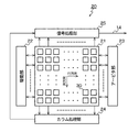
- FIG. 2 is a block diagram showing an example of the configuration of the imaging device according to the first configuration example, which is used as the imaging device 20 in the imaging system 10 to which the technique according to the present disclosure is applied.
- the image pickup device 20 is an asynchronous type image pickup device called DVS, and is a pixel array unit 21, a drive unit 22, and an arbiter unit (arbitration unit). ) 23, a column processing unit 24, and a signal processing unit 25.
- DVS asynchronous type image pickup device
- arbiter unit arbitration unit
- a plurality of pixels 30 are two-dimensionally arranged in a matrix (array shape) in the pixel array unit 21.
- a vertical signal line VSL which will be described later, is wired for each pixel sequence with respect to this matrix-like pixel array.
- Each of the plurality of pixels 30 generates an analog signal having a voltage corresponding to the photocurrent as a pixel signal. Further, each of the plurality of pixels 30 detects the presence or absence of an address event depending on whether or not the amount of change in the photocurrent exceeds a predetermined threshold value. Then, when the address event occurs, the pixel 30 outputs the request to the arbiter unit 23.
- the drive unit 22 drives each of the plurality of pixels 30 to output the pixel signal generated by each pixel 30 to the column processing unit 24.
- the arbiter unit 23 arbitrates the requests from each of the plurality of pixels 30, and transmits a response based on the arbitration result to the pixels 30.
- the pixel 30 that has received the response from the arbiter unit 23 supplies a detection signal (address event detection signal) indicating the detection result to the drive unit 22 and the signal processing unit 25.
- a detection signal address event detection signal
- the column processing unit 24 is composed of, for example, an analog-digital converter, and performs a process of converting an analog pixel signal output from the pixels 30 of the pixel array unit 21 into a digital signal for each pixel array of the pixel array unit 21. Then, the column processing unit 24 supplies the digital signal after the analog-to-digital conversion to the signal processing unit 25.
- the signal processing unit 25 executes predetermined signal processing such as CDS (Correlated Double Sampling) processing and image recognition processing on the digital signal supplied from the column processing unit 24. Then, the signal processing unit 25 supplies the data indicating the processing result and the detection signal supplied from the arbiter unit 23 to the recording unit 12 (see FIG. 1) via the signal line 14.
- predetermined signal processing such as CDS (Correlated Double Sampling) processing and image recognition processing
- FIG. 3 is a block diagram showing an example of the configuration of the pixel array unit 21.
- each of the plurality of pixels 30 has a light receiving unit 31, a pixel signal generation unit 32, and an address event detection unit 33. ing.
- the light receiving unit 31 photoelectrically converts the incident light to generate a photocurrent. Then, the light receiving unit 31 supplies the photocurrent generated by photoelectric conversion to either the pixel signal generation unit 32 or the address event detection unit 33 under the control of the drive unit 22 (see FIG. 2).
- the pixel signal generation unit 32 generates a signal having a voltage corresponding to the optical current supplied from the light receiving unit 31 as a pixel signal SIG, and the generated pixel signal SIG is generated by the column processing unit 24 via the vertical signal line VSL (FIG. FIG. 2).
- the address event detection unit 33 detects the presence or absence of an address event depending on whether or not the amount of change in the photocurrent from each of the light receiving units 31 exceeds a predetermined threshold value.
- the address event includes, for example, an on-event indicating that the amount of change in photocurrent exceeds the upper limit threshold value and an off-event indicating that the amount of change has fallen below the lower limit threshold value.
- the address event detection signal is composed of, for example, one bit indicating the on-event detection result and one bit indicating the off-event detection result.
- the address event detection unit 33 may be configured to detect only on-events.
- the address event detection unit 33 When an address event occurs, the address event detection unit 33 supplies a request for transmitting an address event detection signal to the arbiter unit 23 (see FIG. 2). Then, when the address event detection unit 33 receives the response to the request from the arbiter unit 23, the address event detection unit 33 supplies the address event detection signal to the drive unit 22 and the signal processing unit 25.
- FIG. 4 is a circuit diagram showing an example of the circuit configuration of the pixel 30. As described above, each of the plurality of pixels 30 has a light receiving unit 31, a pixel signal generation unit 32, and an address event detection unit 33.
- the light receiving unit 31 has a light receiving element (photoelectric conversion element) 311, a transfer transistor 312, and an OFG (Over Flow Gate) transistor 313.
- a light receiving element photoelectric conversion element
- a transfer transistor 312 As the transfer transistor 312 and the OFG transistor 313, for example, an N-type MOS (Metal Oxide Semiconductor) transistor is used.
- the transfer transistor 312 and the OFG transistor 313 are connected in series with each other.
- the light receiving element 311 is connected between the common connection node N 1 of the transfer transistor 312 and the OFG transistor 313 and the ground, and performs photoelectric conversion of the incident light to generate a charge amount corresponding to the light amount of the incident light. do.
- the transfer signal TRG is supplied from the drive unit 22 shown in FIG. 2 to the gate electrode of the transfer transistor 312.
- the transfer transistor 312 supplies the charge photoelectrically converted by the light receiving element 311 to the pixel signal generation unit 32 in response to the transfer signal TRG.
- a control signal OFG is supplied from the drive unit 22 to the gate electrode of the OFG transistor 313.
- the OFG transistor 313 supplies the electric signal generated by the light receiving element 311 to the address event detection unit 33 in response to the control signal OFG.
- the electrical signal supplied to the address event detection unit 33 is a photocurrent composed of electric charges.
- the pixel signal generation unit 32 has a reset transistor 321 and an amplification transistor 322, a selection transistor 323, and a floating diffusion layer 324.
- a reset transistor 321 and an amplification transistor 322, a selection transistor 323, and a floating diffusion layer 324 As the reset transistor 321 and the amplification transistor 322 and the selection transistor 323, for example, an N-type MOS transistor is used.
- the pixel signal generation unit 32 is supplied with electric charges that have been photoelectrically converted by the light receiving element 311 by the transfer transistor 312 from the light receiving unit 31.
- the electric charge supplied from the light receiving unit 31 is accumulated in the floating diffusion layer 324.
- the floating diffusion layer 324 generates a voltage signal having a voltage value corresponding to the amount of accumulated charge. That is, the floating diffusion layer 324 converts the electric charge into a voltage.
- the reset transistor 321 is connected between the power supply line of the power supply voltage V DD and the floating diffusion layer 324.
- a reset signal RST is supplied from the drive unit 22 to the gate electrode of the reset transistor 321.
- the reset transistor 321 initializes (reset) the charge amount of the floating diffusion layer 324 in response to the reset signal RST.
- the amplification transistor 322 is connected in series with the selection transistor 323 between the power supply line of the power supply voltage V DD and the vertical signal line VSL.
- the amplification transistor 322 amplifies the charge-voltage-converted voltage signal in the floating diffusion layer 324.
- the selection signal SEL is supplied from the drive unit 22 to the gate electrode of the selection transistor 323.
- the selection transistor 323 outputs the voltage signal amplified by the amplification transistor 322 as a pixel signal SIG to the column processing unit 24 (see FIG. 2) via the vertical signal line VSL.
- the drive unit 22 receives a light receiving unit when the control unit 13 shown in FIG. 1 instructs the start of detection of an address event.
- the control unit 13 shown in FIG. 1 instructs the start of detection of an address event.
- the OFG transistor 313 is driven to supply an optical current to the address event detection unit 33.
- the drive unit 22 turns off the OFG transistor 313 of the pixel 30 and stops the supply of the photocurrent to the address event detection unit 33.
- the drive unit 22 drives the transfer transistor 312 by supplying the transfer signal TRG to the transfer transistor 312, and transfers the charge photoelectrically converted by the light receiving element 311 to the floating diffusion layer 324.
- the power consumption of the image pickup apparatus 20 and the amount of image processing can be reduced as compared with the case where the pixel signals of all the pixels are output regardless of the presence or absence of the address event.
- the configuration of the pixel 30 illustrated here is an example, and is not limited to this configuration example.
- a pixel configuration that does not include the pixel signal generation unit 32 may be used.
- the OFG transistor 313 may be omitted in the light receiving unit 31, and the transfer transistor 312 may have the function of the OFG transistor 313.
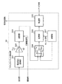
- FIG. 5 is a block diagram showing a first configuration example of the address event detection unit 33.
- the address event detection unit 33 according to this configuration example has a current / voltage conversion unit 331, a buffer 332, a subtractor 333, a quantizer 334, and a transfer unit 335.
- the current-voltage conversion unit 331 converts the photocurrent from the light receiving unit 31 of the pixel 30 into a logarithmic voltage signal.
- the current-voltage conversion unit 331 supplies the converted voltage signal to the buffer 332.
- the buffer 332 buffers the voltage signal supplied from the current-voltage conversion unit 331 and supplies it to the subtractor 333.
- a row drive signal is supplied to the subtractor 333 from the drive unit 22.
- the subtractor 333 lowers the level of the voltage signal supplied from the buffer 332 according to the row drive signal. Then, the subtractor 333 supplies the voltage signal after the level drop to the quantizer 334.
- the quantizer 334 quantizes the voltage signal supplied from the subtractor 333 into a digital signal and outputs it to the transfer unit 335 as an address event detection signal.
- the transfer unit 335 transfers the detection signal of the address event supplied from the quantizer 334 to the arbiter unit 23 and the like.
- the transfer unit 335 supplies the arbiter unit 23 with a request for transmitting an address event detection signal. Then, when the transfer unit 335 receives the response to the request from the arbiter unit 23, the transfer unit 335 supplies the detection signal of the address event to the drive unit 22 and the signal processing unit 25.
- FIG. 6 is a circuit diagram showing an example of the configuration of the current-voltage conversion unit 331 in the address event detection unit 33.
- the current-voltage conversion unit 331 according to this example has a circuit configuration including an N-type transistor 3311, a P-type transistor 3312, and an N-type transistor 3313.
- transistors 3311 to 3313 for example, MOS transistors are used.
- the N-type transistor 3311 is connected between the power supply line of the power supply voltage V DD and the signal input line 3314.
- the P-type transistor 3312 and the N-type transistor 3313 are connected in series between the power supply line of the power supply voltage V DD and the ground.
- the gate electrode of the N-type transistor 3311 and the input terminal of the buffer 332 shown in FIG. 5 are connected to the common connection node N 2 of the P-type transistor 3312 and the N-type transistor 3313.
- a predetermined bias voltage V bias is applied to the gate electrode of the P-type transistor 3312.
- the P-type transistor 3312 supplies a constant current to the N-type transistor 3313.
- a photocurrent is input from the light receiving unit 31 to the gate electrode of the N-type transistor 3313 through the signal input line 3314.
- the drain electrodes of the N-type transistor 3311 and the N-type transistor 3313 are connected to the power supply side, and such a circuit is called a source follower.
- the photocurrent from the light receiving unit 31 is converted into a logarithmic voltage signal by these two source followers connected in a loop.
- FIG. 7 is a circuit diagram showing an example of the configuration of the subtractor 333 and the quantizer 334 in the address event detection unit 33.
- the subtractor 333 has a configuration including a capacitance element 3331, an inverter circuit 3332, a capacitance element 3333, and a switch element 3334.
- One end of the capacitance element 3331 is connected to the output terminal of the buffer 332 shown in FIG. 5, and the other end is connected to the input terminal of the inverter circuit 3332.
- the capacitance element 3333 is connected in parallel to the inverter circuit 3332.
- the switch element 3334 is connected between both ends of the capacitance element 3333.
- a row drive signal is supplied from the drive unit 22 to the switch element 3334 as an open / close control signal.
- the switch element 3334 opens and closes a path connecting both ends of the capacitance element 3333 in response to a row drive signal.
- the inverter circuit 3332 inverts the polarity of the voltage signal input via the capacitance element 3331.
- the charge Q 2 stored in the capacitance element 3333 is expressed by the following equation (3), where the capacitance value of the capacitance element 3333 is C 2 and the output voltage is V out.
- Q 2 -C 2 x V out ... (3)
- Equation (5) represents the subtraction operation of the voltage signal, and the gain of the subtraction result is C 1 / C 2 . Since it is usually desired to maximize the gain, it is preferable to design C 1 to be large and C 2 to be small. On the other hand, if C 2 is too small, kTC noise may increase and the noise characteristics may deteriorate . Therefore, the capacity reduction of C 2 is limited to the range in which noise can be tolerated. Further, since the address event detection unit 33 including the subtractor 333 is mounted on each pixel 30, the capacitance element 3331 and the capacitance element 3333 have an area limitation. In consideration of these, the capacitance values C 1 and C 2 of the capacitance elements 3331 and 3333 are determined.
- the quantizer 334 is configured to have a comparator 3341.
- the comparator 3341 has an output signal of the inverter circuit 3332, that is, a voltage signal from the subtractor 430 as a non-inverting (+) input, and a predetermined threshold voltage V th as an inverting ( ⁇ ) input. Then, the comparator 3341 compares the voltage signal from the subtractor 430 with the predetermined threshold voltage V th, and outputs a signal indicating the comparison result to the transfer unit 335 as an address event detection signal.
- FIG. 8 is a block diagram showing a second configuration example of the address event detection unit 33.
- the address event detection unit 33 includes a storage unit 336 and a storage unit 336 in addition to the current-voltage conversion unit 331, the buffer 332, the subtractor 333, the quantizer 334, and the transfer unit 335. It is configured to have a control unit 337.
- the storage unit 336 is provided between the quantizer 334 and the transfer unit 335, and based on the sample signal supplied from the control unit 337, the output of the quantizer 334, that is, the comparison result of the comparator 3341 is displayed. accumulate.
- the storage unit 336 may be a sampling circuit such as a switch, plastic, or capacitance, or may be a digital memory circuit such as a latch or flip-flop.
- the control unit 337 supplies a predetermined threshold voltage V th to the inverting ( ⁇ ) input terminal of the comparator 3341.
- the threshold voltage V th supplied from the control unit 337 to the comparator 3341 may have different voltage values in time division. For example, the control unit 337 sets the threshold voltage V th1 corresponding to the on-event indicating that the amount of change in the optical current exceeds the upper limit threshold value and the off-event indicating that the amount of change has fallen below the lower limit threshold value.
- one comparator 3341 can detect a plurality of types of address events.
- the storage unit 336 uses, for example, the threshold voltage V th1 corresponding to the on-event during the period in which the threshold voltage V th2 corresponding to the off-event is supplied from the control unit 337 to the inverting (-) input terminal of the comparator 3341.
- the comparison result of the comparator 3341 that has been used may be accumulated.
- the storage unit 336 may be inside the pixel 30 or outside the pixel 30. Further, the storage unit 336 is not an essential component of the address event detection unit 33. That is, the storage unit 336 may be omitted.
- Imaging device is an asynchronous imaging device that reads an event by an asynchronous reading method.
- the event reading method is not limited to the asynchronous reading method, and may be a synchronous reading method.
- the imaging device to which the synchronous reading method is applied is a scanning type imaging device, which is the same as a normal imaging device that performs imaging at a predetermined frame rate.
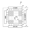
- FIG. 9 is a block diagram showing an example of the configuration of the imaging device according to the second configuration example, that is, the scanning type imaging device, which is used as the imaging device 20 in the imaging system 10 to which the technique according to the present disclosure is applied. ..
- the image pickup device 20 includes a pixel array unit 21, a drive unit 22, a signal processing unit 25, a read area selection unit 27, and a signal generation unit. It is configured to include 28.
- the pixel array unit 21 includes a plurality of pixels 30.
- the plurality of pixels 30 output an output signal in response to the selection signal of the read area selection unit 27.
- Each of the plurality of pixels 30 may have a quantizer in the pixel, as shown in FIG. 7, for example.
- the plurality of pixels 30 output an output signal corresponding to the amount of change in light intensity. As shown in FIG. 9, the plurality of pixels 30 may be two-dimensionally arranged in a matrix.
- the drive unit 22 drives each of the plurality of pixels 30 to output the pixel signal generated by each pixel 30 to the signal processing unit 25.
- the drive unit 22 and the signal processing unit 25 are circuit units for acquiring gradation information. Therefore, when only the event information is acquired, the drive unit 22 and the signal processing unit 25 may be omitted.
- the read area selection unit 27 selects a part of the plurality of pixels 30 included in the pixel array unit 21. For example, the read area selection unit 27 selects any one or a plurality of rows included in the structure of the two-dimensional matrix corresponding to the pixel array unit 21. The read area selection unit 27 sequentially selects one or a plurality of rows according to a preset cycle. Further, the read area selection unit 27 may determine the selection area in response to a request from each pixel 30 of the pixel array unit 21.
- the signal generation unit 28 generates an event signal corresponding to the active pixel that has detected an event among the selected pixels, based on the output signal of the pixel selected by the read area selection unit 27.
- An event is an event in which the intensity of light changes.
- An active pixel is a pixel in which the amount of change in light intensity corresponding to an output signal exceeds or falls below a preset threshold value.
- the signal generation unit 28 compares the output signal of the pixel with the reference signal, detects the active pixel that outputs the output signal when it is larger or smaller than the reference signal, and generates an event signal corresponding to the active pixel. ..
- the signal generation unit 28 can be configured to include, for example, a column selection circuit that arbitrates the signal entering the signal generation unit 28. Further, the signal generation unit 28 can be configured to output not only the information of the active pixel that detected the event but also the information of the inactive pixel that does not detect the event.
- the signal generation unit 28 outputs the address information and the time stamp information (for example, (X, Y, T)) of the active pixel that detected the event through the output line 15.
- the data output from the signal generation unit 28 may be not only address information and time stamp information but also frame format information (for example, (0, 0, 1, 0, ...)). ..
- FIG. 10 is an exploded perspective view showing an outline of the laminated chip structure of the image pickup apparatus 20.
- the laminated chip structure is a structure in which at least two chips of the light receiving chip 201, which is the first chip, and the detection chip 202, which is the second chip, are laminated. It has become. Then, in the circuit configuration of the pixel 30 shown in FIG. 4, each of the light receiving elements 311 is arranged on the light receiving chip 201, and all the elements other than the light receiving element 311 and the elements of the other circuit parts of the pixel 30 are detected chips. Placed on 202.
- the light receiving chip 201 and the detection chip 202 are electrically connected via a connecting portion such as a via (VIA), a Cu—Cu junction, or a bump.
- each element of the light receiving unit 31 is arranged on the light receiving chip 201, and elements other than the light receiving unit 31 and elements of other circuit parts of the pixel 30 are arranged on the detection chip 202. It can be configured to be. Further, each element of the light receiving unit 31, the reset transistor 321 of the pixel signal generation unit 32, and the floating diffusion layer 324 can be arranged on the light receiving chip 201, and the other elements can be arranged on the detection chip 202. .. Further, a part of the elements constituting the address event detection unit 33 can be arranged on the light receiving chip 201 together with the elements of the light receiving unit 31 and the like.
- FIG. 11 is a block diagram showing an example of the configuration of the column processing unit 24 of the image pickup apparatus 20 according to the first configuration example.
- the column processing unit 24 according to this example has a configuration having a plurality of analog-to-digital converters (ADCs) 241 arranged for each pixel row of the pixel array unit 21.
- ADCs analog-to-digital converters
- the configuration example in which the analog-to-digital converter 241 is arranged in a one-to-one correspondence with the pixel sequence of the pixel array unit 21 is illustrated here, the configuration example is not limited to this configuration example.
- the analog-to-digital converter 241 may be arranged in units of a plurality of pixel sequences, and the analog-to-digital converter 241 may be used in a time division manner among the plurality of pixel sequences.
- the analog-digital converter 241 converts the analog pixel signal SIG supplied via the vertical signal line VSL into a digital signal having a larger number of bits than the above-mentioned address event detection signal. For example, if the detection signal of the address event is 2 bits, the pixel signal is converted into a digital signal of 3 bits or more (16 bits or the like). The analog-digital converter 241 supplies the digital signal generated by the analog-to-digital conversion to the signal processing unit 25.
- the image pickup apparatus 20 has a detection unit (that is, an address event detection unit 33) that detects in real time as an address event that the amount of light of the pixel exceeds a predetermined threshold value for each pixel address. It is an asynchronous type imaging device called DVS provided for each pixel 30.
- the imaging device In the imaging device according to the first configuration example of the asynchronous type, originally, when some event (that is, a true event) occurs in the scene, the data that causes the occurrence of the true event is acquired.
- data may be acquired unnecessarily due to noise events (false events) such as sensor noise even in a scene where no true event occurs. This not only reads out the noise signal, but also reduces the throughput of the signal output.
- the image pickup apparatus 20 of the present disclosure described below is designed so as not to acquire a noise event.
- FIG. 12 is a diagram illustrating the reason why flicker occurs.
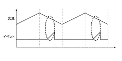
- FIG. 12 is a diagram showing a waveform w1 of a commercial power supply voltage, a brightness fluctuation waveform w2 of an electric appliance, and an event detection signal waveform w3 caused by flicker.
- the commercial power supply voltage is, for example, an AC voltage having a frequency of 50 Hz, and one cycle is 20 ms.
- the brightness of the electric appliance driven by the commercial power supply voltage fluctuates every half cycle of the commercial power supply voltage.
- the address event detection unit 33 described above generates a Positive event (hereinafter referred to as a Pos event) when the absolute value of the amount of change in brightness when the brightness changes in the direction of increasing brightness exceeds the first threshold value, and the brightness is low.
- Negative hereinafter referred to as Neg event
- the Pos event and the Neg event occur alternately in a cycle of 1/2 of the cycle of the luminance fluctuation.
- the image pickup apparatus 20 Since the Pos event and the Neg event caused by the flicker are different from the event originally desired to be detected, the image pickup apparatus 20 according to the present embodiment is characterized in that the event caused by the flicker is not generated.
- FIGS. 13A, 13B and 13C are diagrams showing specific examples of waveforms w4 and w5 of Pos event and Neg event caused by flicker generated in various electric appliances.
- FIG. 13A shows a fire hydrant LED
- FIG. 13B shows an old display monitor device
- FIG. 13C shows a Pos event waveform and a Neg event waveform of a fluorescent lamp.
- the number and duration of Pos events and Neg events differ depending on the type of electric appliance.
- 13A, 13B, and 13C are examples of event occurrence situations, and even if the electric appliances of the same type are used, the occurrence situations of Pos event and Neg event can be changed depending on the individual electric appliances.
- FIG. 14 is a block diagram showing an example of the internal configuration of the signal processing unit 25 according to the present embodiment.
- the signal processing unit 25 of FIG. 14 includes a first detection unit 51, a flicker determination unit 52, and a second detection unit. It has a part 53 and.
- the first detection unit 51 and the flicker determination unit 52 are collectively referred to as a flicker detection unit 54.
- the first detection unit 51 detects a detection signal when the absolute value of the amount of change in the electric signal generated by the plurality of photoelectric conversion elements exceeds a predetermined threshold value.
- the first detection unit 51 detects the event signal output from the address event detection unit 33 as a detection signal.
- the first detection unit 51 has, for example, an event counter 55 and a shift register 56.
- the event counter 55 counts the number of Pos events and the number of Neg events.
- a counter for counting the number of Pos events and a counter for counting the number of Neg events may be provided.
- a counter may be provided that counts up each time a Pos event occurs and counts down each time a Neg event occurs.
- the shift register 56 holds the count value of the event counter 55.
- a memory or a register for holding the count value may be provided.
- the flicker determination unit 52 determines whether or not the detection signal detected by the first detection unit 51 includes a detection signal caused by the flicker of the light source. As will be described later, the flicker determination unit 52 determines whether the detection signal detected by the first detection unit 51 is due to flicker or other factors.
- the second detection unit 53 detects the detection signal of the factor other than the flicker from the detection signals detected by the first detection unit 51.
- FIG. 15 is a diagram illustrating the processing operation of the flicker detection unit 54 having the first detection unit 51 and the flicker determination unit 52.
- FIG. 15 shows an example in which light that causes flicker is incident on the image pickup apparatus 20. As shown in the waveform w6 of FIG. 15, the brightness of the flicker changes periodically.
- FIG. 15 shows the number of pixels Npi that detected the Pos event, the number of pixels Nni that detected the Neg event, the information recognized by the flicker determination unit 52 as the period during which the Pos event occurred (the period during which the Pos event occurred), and the Neg event.
- the information recognized as the occurrence section (Neg event occurrence period) is shown.
- the flicker determination unit 52 recognizes that the Pos event occurrence period is when the value obtained by subtracting Nni from Npi (Npi-Nni) exceeds the predetermined value, and the value obtained by subtracting Npi from Nni (Nni-Npi) sets the predetermined value. If it exceeds, it is recognized as the Neg event occurrence period. If the frequency of flicker is low, both the Pos event occurrence period and the Neg event occurrence period can be zero.
- both the cycle of the Pos event occurrence period and the cycle of the Neg event occurrence period are the same as the fluctuation cycle of the flicker. Therefore, the flicker determination unit 52 determines that the Pos event and the Neg event are caused by the flicker.
- FIG. 16 is a flowchart showing a first example of the processing operation of the flicker detection unit 54.
- FIG. 16 shows the processing operation of the flicker detection unit 54 in the scanning type image pickup apparatus 20 of FIG.
- FIG. 16 shows an example in which Pos events and Neg events are alternately detected by time division.
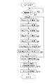
- step S1 it waits until the imaging of one frame by the imaging device 20 is completed (step S1), and reads out the output signals of each pixel in order.
- step S2 the first detection unit 51 acquires the Pos event (step S3).
- the first detection unit 51 stores the acquired Pos event (step S4).
- the first detection unit 51 After the Pos event is detected, it is detected whether or not a Neg event has occurred, and if the Neg event is detected (step S5), the first detection unit 51 acquires the Neg event (step S6). The first detection unit 51 outputs a Pos event and a Neg event (step S7).
- the flicker determination unit 52 counts the number of Pos events and the number of Neg events (step S8). Then, the flicker determination unit 52 compares the count number of the Pos event with the count number of the Neg event (step S9).
- step S2 If the detection of the Pos event and the Neg event for all the pixels in the image pickup apparatus 20 has not been completed, the processing of step S2 and subsequent steps is repeated.
- the comparison result of the count numbers of the Pos event and the Neg event is held (step S10). The comparison result is retained within an arbitrary number of frames.
- step S11 based on the comparison result of the count numbers of the Pos event and the Neg event, it is determined whether or not the Pos event and the Neg event are caused by flicker, and the determination result is output (step S11).
- FIG. 17 is a flowchart showing a second example of the processing operation of the flicker detection unit 54.
- FIG. 17 shows the processing operation of the flicker detection unit 54 in the scanning type image pickup apparatus 20 of FIG.
- FIG. 17 shows an example of reading the Pos event and the Neg event in parallel.
- step S21 it waits until the imaging of one frame by the imaging device 20 is completed (step S21), and reads out the output signals of each pixel in order.
- step S22 the first detection unit 51 acquires the Pos event or Neg event (step S23).
- the flicker determination unit 52 counts the number of Pos events and the number of Neg events (step S24). Then, the flicker determination unit 52 compares the count number of the Pos event with the count number of the Neg event (step S25).
- step S22 If the detection of the Pos event and the Neg event for all the pixels in the image pickup apparatus 20 has not been completed, the processes after step S22 are repeated.
- the comparison result of the Pos event and the Neg event is retained (step S26). The comparison result is retained within an arbitrary number of frames.
- step S27 based on the comparison result of the count numbers of the Pos event and the Neg event, it is determined whether or not the Pos event and the Neg event are caused by flicker, and the determination result is output (step S27).
- FIG. 18 is a flowchart showing a third example of the processing operation of the flicker detection unit 54.
- FIG. 18 shows the processing operation of the flicker detection unit 54 in the asynchronous imaging device 20 of FIG.
- FIG. 18 shows an example in which event detection is performed asynchronously for each row of the pixel array unit.
- step S31 it waits until the Pos event or Neg event occurs (step S31), and when the Pos event or Neg event is detected (step S32), the first detection unit 51 acquires the Pos event or Neg event (step S31). S33).
- the flicker determination unit 52 counts the number of Pos events and the number of Neg events (step S34). Then, the flicker determination unit 52 compares the count number of the Pos event with the count number of the Neg event (step S35). Next, the comparison result of the count number is accumulated for an arbitrary period (step S36). Next, the accumulated comparison results are retained for an arbitrary period (step S37).
- step S32 If the Pos event and Neg event have not been counted yet, the processing after step S32 is repeated.
- FIG. 19 is a flowchart showing a fourth example of the processing operation of the flicker detection unit 54.
- FIG. 19 shows the processing operation of the flicker detection unit 54 in the asynchronous imaging device 20 of FIG.
- FIG. 19 shows an example in which event detection is performed asynchronously for each pixel of the pixel array unit.
- step S41 it waits until the Pos event or Neg event occurs (step S41), and when the Pos event or Neg event is detected (step S42), the first detection unit 51 acquires the Pos event or Neg event (step S41). S43).
- the flicker determination unit 52 counts up the counter when a Pos event is detected, and counts down the counter when a Neg event is detected (step S44). Then, the count value of the counter is held for an arbitrary period (step S45).
- step S42 If the detection processing of all the generated Pos events and Neg events has not been completed, the processing of step S42 and subsequent steps is repeated.
- the comparison result of the Pos event and the Neg event is held based on the count value of the counter (step S46).
- the retention period is arbitrary.
- step S47 based on the count value of the counter, it is determined whether or not the Pos event and the Neg event are caused by flicker, and the determination result is output (step S47).
- step S11 of FIG. 16 step S27 of FIG. 17, step S37 of FIG. 18, and step S47 of FIG. 19, the Pos event and the Neg event are flicker when any of the following 1) to 3) is satisfied. Is determined to be a factor.
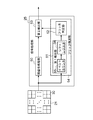
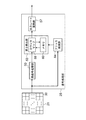
- FIG. 20 is a block diagram showing a first specific example of the signal processing unit 25.
- the signal processing unit 25 of FIG. 20 includes a flicker detection unit 54 having a first detection unit 51 and a flicker determination unit 52 similar to those of FIG. 14, and also includes an output rate conversion unit 57.
- a pixel control circuit 58 is connected to the signal processing unit 25 of FIG. 20.
- the pixel control circuit 58 corresponds to the second detection unit 53 in FIG.
- the pixel control circuit 58 may be provided inside the signal processing unit 25.
- the pixel control circuit 58 sets the event detection period according to the flicker cycle based on the result determined by the flicker determination unit 52.
- the pixel control circuit 58 sends a signal indicating an event detection period to the address event detection unit 33 in the pixel array unit 21.
- the address event detection unit 33 performs event detection within the event detection period set by the pixel control circuit 58. This makes it possible to detect an event different from the event caused by the flicker.
- the pixel control circuit 58 when the flicker determination unit determines that the flicker-caused detection signal is included, the pixel control circuit 58 has a cycle detection unit that detects the flicker cycle and a flicker cycle detected by the cycle detection unit. It has a function with a detection period setting unit that sets the detection period of the detection signal according to the above.
- the signal processing unit 25 and the pixel control circuit 58 in FIG. 20 analogally control the period during which the address event detection unit 33 detects an event.
- the event detection period is set in an analog manner so that the cycle of the Pos event caused by the flicker and the cycle of the Neg event are different.
- the block diagram of FIG. 20 is applicable to the scanning type imaging device 20 and cannot be applied to the asynchronous type imaging device 20.
- the reason is that the address event detection unit 33 detects the event only during the event detection period set by the pixel control circuit 58, and cannot perform the event detection asynchronously.
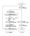
- FIG. 21 is a flowchart showing the processing operation of the signal processing unit 25 of FIG. Steps S52 to S57 of FIG. 21 are flicker detection paths, and steps S58 to S59 are data paths after flicker detection is completed.
- the flicker detection unit 54 When an event is detected (step S51), the flicker detection unit 54 performs a process of detecting whether or not the detected event is caused by flicker (step S52). The detection result of the flicker detection unit 54 is received (step S53), and it is determined whether or not the flicker is a factor event (step S54).
- the flicker detection unit 54 calculates the flicker cycle (step S55) and transmits the calculated flicker cycle to the pixel control circuit 58 (step S56).
- the pixel control circuit 58 sets the event detection period according to the flicker cycle based on the flicker cycle (step S57).
- the address event detection unit 33 detects the event within the event detection period.
- the event detected and output by the address event detection unit 33 is detected in step S51, and then the output rate of the event is converted by the output rate conversion unit 57 (step S58). Since the address event detection unit 33 detects the event only within the event detection period, the output frequency of the event decreases, so that the output rate conversion unit 57 controls to lower the output rate.
- the signal processing unit 25 outputs an event signal having an output rate corresponding to the length of the event detection period (step S59).
- FIG. 22 is a block diagram showing a second specific example of the signal processing unit 25.
- the signal processing unit 25 of FIG. 22 includes a first detection unit 51, a flicker determination unit 52, a second detection unit 53, and an output rate conversion unit 57, but the one corresponding to the pixel control circuit 58 of FIG. 21 is Not provided.
- the flicker detection unit 54 in FIG. 22 notifies the second detection unit 53 of the presence or absence of flicker and the length of one cycle of flicker.
- the second detection unit 53 has a counter map 59 and a memory 60 for storing the information of the counter map 59.
- the counter map 59 is an aggregate of counters 59a corresponding to each pixel of the pixel array unit 21.
- Each counter 59a counts up when a Pos event is detected and counts down when a Neg event is detected for the corresponding pixel in order to count the events that occur within the cycle notified by the flicker detection unit 54.
- the count value of the pixel counter 59a in which only the event caused by the flicker occurs is zero.
- the count value of the counter 59a of the pixel in which an event caused by a factor other than flicker has occurred becomes a value other than zero.
- the memory 60 stores the count value of each counter 59a of the counter map 59.
- the flicker detection unit 54 determines that the flicker-caused detection signal is included
- the second detection unit 53 of FIG. 22 counts the number of events detected within the flicker cycle. Detects the number of occurrences of events caused by factors other than flicker.
- the signal processing unit 25 of FIG. 22 determines whether the event is caused by flicker or a factor other than flicker based on the count value of each counter 59a of the counter map 59, and detects the event by digital processing. Is going.
- the processing of the signal processing unit 25 of FIG. 22 can be applied to both the asynchronous imaging device 20 of FIG. 2 and the scanning imaging device 20 of FIG.
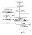
- FIG. 24 is a flowchart showing the processing operation of the signal processing unit 25 of FIG. 22. Steps S62 to S65 in FIG. 24 are flicker detection paths, and steps S66 to S70 are data paths performed after flicker detection.
- step S61 to S65 the flicker cycle is calculated in the same manner as in steps S51 to S55 of FIG.
- step S66 the counter map 59 of FIG. 22 is used to count up or down the counter 59a corresponding to the detected Pos event or Neg event.
- step S67 each count value of the counter map 59 is filtered (step S67). For example, in step S67, among the count values of the counter map 59, the count value considered to be due to noise is corrected.
- the count values far from zero are considered to be events caused by factors other than flicker, so that event is output.
- step S68 one of the event detected by the counter map 59 and the event detected by the first detection unit 51 is selected.
- the event detected by the counter map 59 is selected, and when it is determined that there is no event caused by flicker, the first detection unit 51 Select the event detected in.
- the output rate of the selected event is converted by the output rate conversion unit 57 as needed (step S69), and the event is output (step S70).
- FIGS. 20 to 24 described above show an example in which the event detected by the address event detection unit 33 is filtered by the signal processing unit 25 by analog processing or digital processing, but the nature of the event caused by flicker is shown. You may detect an event caused by a factor other than flicker by paying attention to.
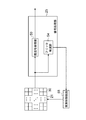
- FIG. 25 is a block diagram showing a third specific example of the signal processing unit 25.
- the signal processing unit 25 of FIG. 25 has a flicker detection unit 54 having a first detection unit 51 and a flicker determination unit 52.
- the signal processing unit 25 is not provided with an output rate control unit.
- a pixel control circuit 58 is connected to the signal processing unit 25 of FIG. 25.
- the pixel control circuit 58 corresponds to the second detection unit 53 of FIG. 14, and is a case where the flicker determination unit 52 determines that an event (detection signal) caused by flicker is included, and is a Pos event.
- an event detection signal
- An event when the absolute value of the amount of change in the direction in which the signal level of the electric signal increases within the period exceeds the first threshold value is detected as an event (detection signal) of a factor other than flicker.
- the pixel control circuit 58 is a factor other than the flicker when the Neg event is generated within the flicker Pos event occurrence period and when the Pos event is generated within the flicker Neg event occurrence period. These events are detected because they are considered to be events of.
- FIG. 26A and 26B are diagrams schematically showing the operation of the pixel control circuit 58.
- FIG. 26A shows an example in which an event in which the brightness increases occurs while the brightness of the light source is decreasing. While the brightness of the light source is decreasing, it is the period during which the Neg event of flicker occurs. During this period, no Pos event is detected from the light source. Therefore, if a Pos event is detected within this period, it can be determined that the event is due to a factor other than flicker.
- FIG. 26B shows an example in which an event in which the brightness decreases occurs while the brightness of the light source is increasing. While the brightness of the light source is increasing, it is the period during which the Pos event of flicker occurs. During this period, no Neg event is detected from the light source. Therefore, if a Neg event is detected within this period, it can be determined that the event is due to a factor other than flicker.
- the pixel control circuit 58 of FIG. 25 detects a Neg event within the flicker Pos event occurrence period by analog processing, and detects a Pos event within the flicker Neg event occurrence period.
- FIG. 27 is a flowchart showing the processing operation of the signal processing unit 25 of FIG. 25. Steps S82 to S87 of FIG. 27 are flicker detection paths, and steps S88 to S89 are data paths performed after flicker detection.
- step S81 When an event is detected (step S81), the flicker detection unit 54 processes (step S82).
- the processing result of the flicker detection unit 54 is received (step S83), and it is determined whether or not the flicker is a factor event (step S84).
- the flicker detection unit 54 estimates the Pos event occurrence period and the Neg event occurrence period (step S85).
- the flicker detection unit 54 transmits the estimated Pos event occurrence period and Neg event occurrence period to the pixel control circuit 58 (step S86).
- the pixel control circuit 58 instructs the address event detection unit 33 to detect the Neg event during the Pos event occurrence period and detect the Pos event during the Neg event occurrence period (step S87).
- Step S88 The output rate of the Neg event within the Pos event occurrence period and the Pos event within the Neg event occurrence period detected by the address event detection unit 33 is converted by the output rate conversion unit 57 (step S88) and output. (Step S89).
- FIG. 28 is a block diagram showing a fourth specific example of the signal processing unit 25.
- the signal processing unit 25 of FIG. 28 includes a first detection unit 51, a flicker determination unit 52, and an event selection unit 61.
- the event selection unit 61 corresponds to the second detection unit 53 in FIG.
- the event selection unit 61 detects a Neg event within the Pos event occurrence period caused by flicker and a Pos event within the Neg event occurrence period. That is, the event selection unit 61 discards the Pos event within the Pos event occurrence period caused by the flicker and detects the Neg event, and also rejects the Neg event within the Neg event occurrence period to detect the Pos event. ..
- FIG. 29 is a flowchart showing the processing operation of the signal processing unit 25 of FIG. 28.
- Steps S92 to S95 in FIG. 29 are flicker detection paths, and steps S96 to S98 are data paths performed after flicker detection.
- steps S91 to S95 is the same as the processing of steps S81 to S85 of FIG.
- the event selection unit 61 discards the Pos event in the Pos event occurrence period caused by the flicker estimated in step S85 to detect the Neg event, and discards the Neg event in the Neg event occurrence period to make the Pos event. Is detected (step S96).
- step S96 If an event caused by flicker has occurred, the event detected in step S96 is selected, and if an event caused by flicker does not occur, the event detected by the first detection unit 51 is selected. Is selected (step S97).
- the signal processing unit 25 outputs the event selected in step S97 (step S98).
- the signal processing unit 25 of FIG. 28 does not include the output rate conversion unit 57, it outputs an event because only a part of the event detected by the address event detection unit 33 is output from the signal processing unit 25. It may be necessary to control the timing.
- FIG. 30 is a flowchart in which FIG. 29 is partially modified.
- Step S99 in FIG. 30 performs a process of delaying the output timing of the event output from the address event detection unit 33.
- the signal delay generated in the processes of steps S92 to S95 can be provided in step S99.
- an event when an event occurs, it is determined whether or not the event is caused by flicker, and only the event caused by something other than flicker is detected. This makes it unaffected by events caused by flicker. More specifically, by detecting the cycle in which flicker occurs and detecting the event that occurs in other than that cycle, it is possible to detect an event caused by a factor other than flicker. Alternatively, since Pos events and Neg events occur alternately in events caused by flicker, events caused by factors other than flicker can be detected by comparing the number of Pos events and the number of Neg events. Alternatively, for events caused by flicker, the Pos event occurrence period in which the Pos event occurs and the Neg event occurrence period in which the Neg event occurs can be predicted in advance. By detecting Pos events that occurred within the occurrence period, it is possible to detect events caused by factors other than flicker.
- the technology according to the present disclosure can be applied to various products. A more specific application example will be described below.
- the technology according to the present disclosure includes any type of movement such as automobiles, electric vehicles, hybrid electric vehicles, motorcycles, bicycles, personal mobility, airplanes, drones, ships, robots, construction machines, agricultural machines (tractors), and the like. It may be realized as a distance measuring device mounted on the body.
- FIG. 31 is a block diagram showing a schematic configuration example of a vehicle control system 7000, which is an example of a mobile control system to which the technique according to the present disclosure can be applied.
- the vehicle control system 7000 includes a plurality of electronic control units connected via the communication network 7010.
- the vehicle control system 7000 includes a drive system control unit 7100, a body system control unit 7200, a battery control unit 7300, an external information detection unit 7400, an in-vehicle information detection unit 7500, and an integrated control unit 7600. ..
- the communication network 7010 connecting these plurality of control units conforms to any standard such as CAN (Controller Area Network), LIN (Local Interconnect Network), LAN (Local Area Network) or FlexRay (registered trademark). It may be an in-vehicle communication network.
- CAN Controller Area Network
- LIN Local Interconnect Network
- LAN Local Area Network
- FlexRay registered trademark
- Each control unit includes a microcomputer that performs arithmetic processing according to various programs, a storage unit that stores a program executed by the microcomputer or parameters used for various arithmetics, and a drive circuit that drives various control target devices. To be equipped.
- Each control unit is provided with a network I / F for communicating with other control units via the communication network 7010, and is provided by wired communication or wireless communication with devices or sensors inside or outside the vehicle. A communication I / F for performing communication is provided. In FIG.
- the functional configuration of the integrated control unit 7600 includes a microcomputer 7610, a general-purpose communication I / F 7620, a dedicated communication I / F 7630, a positioning unit 7640, a beacon receiving unit 7650, an in-vehicle device I / F 7660, and an audio image output unit 7670.
- the vehicle-mounted network I / F 7680 and the storage unit 7690 are shown.
- Other control units also include a microcomputer, a communication I / F, a storage unit, and the like.
- the drive system control unit 7100 controls the operation of the device related to the drive system of the vehicle according to various programs.
- the drive system control unit 7100 provides a driving force generator for generating the driving force of the vehicle such as an internal combustion engine or a driving motor, a driving force transmission mechanism for transmitting the driving force to the wheels, and a steering angle of the vehicle. It functions as a control device such as a steering mechanism for adjusting and a braking device for generating a braking force of a vehicle.
- the drive system control unit 7100 may have a function as a control device such as ABS (Antilock Brake System) or ESC (Electronic Stability Control).
- the vehicle condition detection unit 7110 is connected to the drive system control unit 7100.
- the vehicle state detection unit 7110 may include, for example, a gyro sensor that detects the angular velocity of the axial rotation motion of the vehicle body, an acceleration sensor that detects the acceleration of the vehicle, an accelerator pedal operation amount, a brake pedal operation amount, or steering wheel steering. Includes at least one of the sensors for detecting angular velocity, engine speed, wheel speed, and the like.
- the drive system control unit 7100 performs arithmetic processing using a signal input from the vehicle state detection unit 7110 to control an internal combustion engine, a drive motor, an electric power steering device, a braking device, and the like.
- the body system control unit 7200 controls the operation of various devices mounted on the vehicle body according to various programs.
- the body system control unit 7200 functions as a keyless entry system, a smart key system, a power window device, or a control device for various lamps such as a head lamp, a back lamp, a brake lamp, a winker, or a fog lamp.
- the body system control unit 7200 may be input with radio waves transmitted from a portable device that substitutes for the key or signals of various switches.
- the body system control unit 7200 receives inputs of these radio waves or signals and controls a vehicle door lock device, a power window device, a lamp, and the like.
- the battery control unit 7300 controls the secondary battery 7310, which is the power supply source of the drive motor, according to various programs. For example, information such as the battery temperature, the battery output voltage, or the remaining capacity of the battery is input to the battery control unit 7300 from the battery device including the secondary battery 7310. The battery control unit 7300 performs arithmetic processing using these signals to control the temperature of the secondary battery 7310 or the cooling device provided in the battery device.
- the vehicle outside information detection unit 7400 detects information outside the vehicle equipped with the vehicle control system 7000.
- the imaging unit 7410 and the vehicle exterior information detection unit 7420 is connected to the vehicle exterior information detection unit 7400.
- the imaging unit 7410 includes at least one of a ToF (Time Of Flight) camera, a stereo camera, a monocular camera, an infrared camera, and other cameras.
- the vehicle exterior information detection unit 7420 is used to detect, for example, the current weather or an environment sensor for detecting the weather, or other vehicles, obstacles, pedestrians, etc. around the vehicle equipped with the vehicle control system 7000. At least one of the surrounding information detection sensors is included.
- the environment sensor may be, for example, at least one of a raindrop sensor that detects rainy weather, a fog sensor that detects fog, a sunshine sensor that detects the degree of sunshine, and a snow sensor that detects snowfall.
- the ambient information detection sensor may be at least one of an ultrasonic sensor, a radar device, and a LIDAR (Light Detection and Ranging, Laser Imaging Detection and Ranging) device.
- the imaging unit 7410 and the vehicle exterior information detection unit 7420 may be provided as independent sensors or devices, or may be provided as a device in which a plurality of sensors or devices are integrated.
- FIG. 32 shows an example of the installation positions of the imaging unit 7410 and the vehicle exterior information detection unit 7420.
- the imaging units 7910, 7912, 7914, 7916, 7918 are provided, for example, at at least one of the front nose, side mirrors, rear bumpers, back door, and upper part of the windshield of the vehicle interior of the vehicle 7900.
- the image pickup unit 7910 provided on the front nose and the image pickup section 7918 provided on the upper part of the windshield in the vehicle interior mainly acquire an image in front of the vehicle 7900.
- the imaging units 7912 and 7914 provided in the side mirrors mainly acquire images of the side of the vehicle 7900.
- the image pickup unit 7916 provided on the rear bumper or the back door mainly acquires an image of the rear of the vehicle 7900.
- the imaging unit 7918 provided on the upper part of the windshield in the vehicle interior is mainly used for detecting a preceding vehicle, a pedestrian, an obstacle, a traffic light, a traffic sign, a lane, or the like.
- FIG. 32 shows an example of the photographing range of each of the imaging units 7910, 7912, 7914, 7916.
- the imaging range a indicates the imaging range of the imaging unit 7910 provided on the front nose
- the imaging ranges b and c indicate the imaging ranges of the imaging units 7912 and 7914 provided on the side mirrors, respectively
- the imaging range d indicates the imaging range d.
- the imaging range of the imaging unit 7916 provided on the rear bumper or the back door is shown. For example, by superimposing the image data captured by the imaging units 7910, 7912, 7914, 7916, a bird's-eye view image of the vehicle 7900 as viewed from above can be obtained.
- the vehicle exterior information detection units 7920, 7922, 7924, 7926, 7928, 7930 provided on the front, rear, side, corners of the vehicle 7900 and the upper part of the windshield in the vehicle interior may be, for example, an ultrasonic sensor or a radar device.
- the vehicle exterior information detection units 7920, 7926, 7930 provided on the front nose, rear bumper, back door, and upper part of the windshield in the vehicle interior of the vehicle 7900 may be, for example, a lidar device.
- These out-of-vehicle information detection units 7920 to 7930 are mainly used for detecting a preceding vehicle, a pedestrian, an obstacle, or the like.
- the vehicle exterior information detection unit 7400 causes the image pickup unit 7410 to capture an image outside the vehicle and receives the captured image data. Further, the vehicle exterior information detection unit 7400 receives detection information from the connected vehicle exterior information detection unit 7420. When the vehicle exterior information detection unit 7420 is an ultrasonic sensor, a radar device, or a lidar device, the vehicle exterior information detection unit 7400 transmits ultrasonic waves, electromagnetic waves, or the like, and receives received reflected wave information.
- the vehicle exterior information detection unit 7400 may perform object detection processing or distance detection processing such as a person, a vehicle, an obstacle, a sign, or a character on a road surface based on the received information.
- the vehicle exterior information detection unit 7400 may perform an environment recognition process for recognizing rainfall, fog, road surface conditions, etc. based on the received information.
- the vehicle outside information detection unit 7400 may calculate the distance to an object outside the vehicle based on the received information.
- the vehicle exterior information detection unit 7400 may perform image recognition processing or distance detection processing for recognizing a person, a vehicle, an obstacle, a sign, a character on the road surface, or the like based on the received image data.
- the vehicle exterior information detection unit 7400 performs processing such as distortion correction or alignment on the received image data, and synthesizes the image data captured by different imaging units 7410 to generate a bird's-eye view image or a panoramic image. May be good.
- the vehicle exterior information detection unit 7400 may perform the viewpoint conversion process using the image data captured by different imaging units 7410.
- the in-vehicle information detection unit 7500 detects the in-vehicle information.
- a driver state detection unit 7510 that detects the driver's state is connected to the in-vehicle information detection unit 7500.
- the driver state detection unit 7510 may include a camera that captures the driver, a biosensor that detects the driver's biological information, a microphone that collects sound in the vehicle interior, and the like.
- the biosensor is provided on, for example, the seat surface or the steering wheel, and detects the biometric information of the passenger sitting on the seat or the driver holding the steering wheel.
- the in-vehicle information detection unit 7500 may calculate the degree of fatigue or concentration of the driver based on the detection information input from the driver state detection unit 7510, and may determine whether the driver is dozing or not. You may.
- the in-vehicle information detection unit 7500 may perform processing such as noise canceling processing on the collected audio signal.
- the integrated control unit 7600 controls the overall operation in the vehicle control system 7000 according to various programs.
- An input unit 7800 is connected to the integrated control unit 7600.
- the input unit 7800 is realized by a device such as a touch panel, a button, a microphone, a switch or a lever, which can be input-operated by a passenger. Data obtained by recognizing the voice input by the microphone may be input to the integrated control unit 7600.
- the input unit 7800 may be, for example, a remote control device using infrared rays or other radio waves, or an externally connected device such as a mobile phone or a PDA (Personal Digital Assistant) that supports the operation of the vehicle control system 7000. You may.
- the input unit 7800 may be, for example, a camera, in which case the passenger can input information by gesture. Alternatively, data obtained by detecting the movement of the wearable device worn by the passenger may be input. Further, the input unit 7800 may include, for example, an input control circuit that generates an input signal based on the information input by the passenger or the like using the input unit 7800 and outputs the input signal to the integrated control unit 7600. By operating the input unit 7800, the passenger or the like inputs various data to the vehicle control system 7000 and instructs the processing operation.
- the storage unit 7690 may include a ROM (Read Only Memory) for storing various programs executed by the microcomputer, and a RAM (Random Access Memory) for storing various parameters, calculation results, sensor values, and the like. Further, the storage unit 7690 may be realized by a magnetic storage device such as an HDD (Hard Disc Drive), a semiconductor storage device, an optical storage device, an optical magnetic storage device, or the like.
- ROM Read Only Memory
- RAM Random Access Memory
- the general-purpose communication I / F 7620 is a general-purpose communication I / F that mediates communication with various devices existing in the external environment 7750.
- General-purpose communication I / F7620 is a cellular communication protocol such as GSM (registered trademark) (Global System of Mobile communications), WiMAX, LTE (Long Term Evolution) or LTE-A (LTE-Advanced), or wireless LAN (Wi-Fi).
- GSM Global System of Mobile communications
- WiMAX Wireless F
- LTE Long Term Evolution
- LTE-A Long Term Evolution-A
- Wi-Fi wireless LAN
- Other wireless communication protocols such as (also referred to as (registered trademark)) and Bluetooth (registered trademark) may be implemented.
- the general-purpose communication I / F 7620 connects to a device (for example, an application server or a control server) existing on an external network (for example, the Internet, a cloud network, or a business-specific network) via, for example, a base station or an access point. You may. Further, the general-purpose communication I / F7620 uses, for example, P2P (Peer To Peer) technology, and is a terminal existing in the vicinity of the vehicle (for example, a terminal of a driver, a pedestrian, or a store, or an MTC (Machine Type Communication) terminal). May be connected with.
- P2P Peer To Peer
- MTC Machine Type Communication
- the dedicated communication I / F 7630 is a communication I / F that supports a communication protocol formulated for use in a vehicle.
- the dedicated communication I / F7630 uses a standard protocol such as WAVE (Wireless Access in Vehicle Environment), DSRC (Dedicated Short Range Communications), or a cellular communication protocol, which is a combination of the lower layer IEEE802.11p and the upper layer IEEE1609. May be implemented.
- the dedicated communication I / F7630 typically includes vehicle-to-vehicle (Vehicle to Vehicle) communication, road-to-vehicle (Vehicle to Infrastructure) communication, vehicle-to-home (Vehicle to Home) communication, and pedestrian-to-pedestrian (Vehicle to Pedestrian) communication. ) Carry out V2X communication, which is a concept that includes one or more of the communications.
- the positioning unit 7640 receives, for example, a GNSS signal from a GNSS (Global Navigation Satellite System) satellite (for example, a GPS signal from a GPS (Global Positioning System) satellite), executes positioning, and executes positioning, and the latitude, longitude, and altitude of the vehicle. Generate location information including.
- the positioning unit 7640 may specify the current position by exchanging signals with the wireless access point, or may acquire position information from a terminal such as a mobile phone, PHS, or smartphone having a positioning function.
- the beacon receiving unit 7650 receives radio waves or electromagnetic waves transmitted from a radio station or the like installed on the road, and acquires information such as the current position, traffic jam, road closure, or required time.
- the function of the beacon receiving unit 7650 may be included in the above-mentioned dedicated communication I / F 7630.
- the in-vehicle device I / F 7660 is a communication interface that mediates the connection between the microcomputer 7610 and various in-vehicle devices 7760 existing in the vehicle.
- the in-vehicle device I / F7660 may establish a wireless connection using a wireless communication protocol such as wireless LAN, Bluetooth (registered trademark), NFC (Near Field Communication) or WUSB (Wireless USB).
- a wireless communication protocol such as wireless LAN, Bluetooth (registered trademark), NFC (Near Field Communication) or WUSB (Wireless USB).
- the in-vehicle device I / F7660 is connected via a connection terminal (and a cable if necessary) (not shown), USB (Universal Serial Bus), HDMI (registered trademark) (High-Definition Multimedia Interface), or MHL (Mobile).
- a wired connection such as High-definition Link may be established.
- the in-vehicle device 7760 may include, for example, at least one of a passenger's mobile device or wearable device, or an information device carried or attached to the vehicle.
- the in-vehicle device 7760 may include a navigation device that searches for a route to an arbitrary destination.
- the in-vehicle device I / F 7660 exchanges control signals or data signals with these in-vehicle devices 7760.
- the in-vehicle network I / F7680 is an interface that mediates communication between the microcomputer 7610 and the communication network 7010.
- the vehicle-mounted network I / F7680 transmits and receives signals and the like according to a predetermined protocol supported by the communication network 7010.
- the microcomputer 7610 of the integrated control unit 7600 is via at least one of general-purpose communication I / F7620, dedicated communication I / F7630, positioning unit 7640, beacon receiving unit 7650, in-vehicle device I / F7660, and in-vehicle network I / F7680. Based on the information acquired in the above, the vehicle control system 7000 is controlled according to various programs. For example, the microcomputer 7610 calculates the control target value of the driving force generator, the steering mechanism, or the braking device based on the acquired information inside and outside the vehicle, and outputs a control command to the drive system control unit 7100. May be good.
- the microcomputer 7610 realizes ADAS (Advanced Driver Assistance System) functions including vehicle collision avoidance or impact mitigation, follow-up driving based on inter-vehicle distance, vehicle speed maintenance driving, vehicle collision warning, vehicle lane deviation warning, and the like. Cooperative control may be performed for the purpose of.
- the microcomputer 7610 automatically travels autonomously without relying on the driver's operation by controlling the driving force generator, steering mechanism, braking device, etc. based on the acquired information on the surroundings of the vehicle. Coordinated control for the purpose of driving or the like may be performed.
- ADAS Advanced Driver Assistance System
- the microcomputer 7610 has information acquired via at least one of general-purpose communication I / F7620, dedicated communication I / F7630, positioning unit 7640, beacon receiving unit 7650, in-vehicle device I / F7660, and in-vehicle network I / F7680. Based on the above, three-dimensional distance information between the vehicle and an object such as a surrounding structure or a person may be generated, and local map information including the peripheral information of the current position of the vehicle may be created. Further, the microcomputer 7610 may predict a danger such as a vehicle collision, a pedestrian or the like approaching or entering a closed road based on the acquired information, and may generate a warning signal.
- the warning signal may be, for example, a signal for generating a warning sound or turning on a warning lamp.
- the audio image output unit 7670 transmits the output signal of at least one of the audio and the image to the output device capable of visually or audibly notifying the passenger or the outside of the vehicle of the information.
- an audio speaker 7710, a display unit 7720, and an instrument panel 7730 are exemplified as output devices.
- the display unit 7720 may include, for example, at least one of an onboard display and a heads-up display.
- the display unit 7720 may have an AR (Augmented Reality) display function.
- the output device may be other devices other than these devices, such as headphones, wearable devices such as eyeglass-type displays worn by passengers, and projectors or lamps.
- the display device displays the results obtained by various processes performed by the microcomputer 7610 or the information received from other control units in various formats such as texts, images, tables, and graphs. Display visually.
- the audio output device converts an audio signal composed of reproduced audio data, acoustic data, or the like into an analog signal and outputs the audio signal audibly.
- At least two control units connected via the communication network 7010 may be integrated as one control unit.
- each control unit may be composed of a plurality of control units.
- the vehicle control system 7000 may include another control unit (not shown).
- the other control unit may have a part or all of the functions carried out by any of the control units. That is, as long as information is transmitted and received via the communication network 7010, predetermined arithmetic processing may be performed by any of the control units.
- a sensor or device connected to any control unit may be connected to another control unit, and a plurality of control units may send and receive detection information to and from each other via the communication network 7010. .
- the techniques according to the present disclosure include, for example, the imaging unit 7910, 7912, 7914, 7916, 7918, the vehicle exterior information detection unit 7920, 7922, 7924, 7926, 7928, 7930, and the driver state detection. It can be applied to the part 7510 and the like. Specifically, the imaging system 10 of FIG. 1 having the imaging apparatus of the present disclosure can be applied to these imaging units and detection units.
- the influence of noise events such as sensor noise can be mitigated, and the occurrence of true events can be detected reliably and quickly, thus realizing safe vehicle driving. It becomes possible to do.
- the present technology can have the following configurations.
- a photoelectric conversion unit having a plurality of photoelectric conversion elements, each of which photoelectrically converts incident light to generate an electric signal.
- a first detection unit that detects a detection signal when the absolute value of the amount of change in the electric signal generated by the plurality of photoelectric conversion elements exceeds a predetermined threshold value.
- a flicker determination unit that determines whether or not the detection signal caused by the flicker of the light source is included in the detection signal detected by the first detection unit. When it is determined that the flicker contains a factor detection signal, a second detection unit that detects a detection signal of a factor other than the flicker from the detection signals detected by the first detection unit.
- An image pickup device to be equipped.
- the first detection unit detects the first detection signal when the absolute value of the amount of change in the direction in which the signal level of the electric signal increases exceeds the first threshold value, and also detects the signal level of the electric signal.
- the second detection signal is detected when the absolute value of the amount of change in the direction of decreasing exceeds the second threshold value.
- the flicker determination unit includes the flicker in the detection signals detected by the first detection unit based on the number of the first detection signals and the number of the second detection signals detected within a predetermined period.
- the first detection unit reads out the electric signals of the plurality of photoelectric conversion elements in order, detects one of the first detection signal and the second detection signal, and then the first detection signal and the first detection signal.
- the imaging device according to (2) wherein the other of the second detection signals is detected, and the number of the first detection signal and the second detection signal is counted over a predetermined period.
- the first detection unit sequentially reads out the electric signals of the plurality of photoelectric conversion elements, detects the first detection signal and the second detection signal in parallel, and detects the first detection signal and the first detection signal and the second detection signal in parallel.
- the imaging device according to (2) which counts the number of the second detection signals over a predetermined period.
- the first detection unit is the number of the first detection signal and the second detection signal of the photoelectric conversion element in which the absolute value of the change amount exceeds the threshold value among the plurality of photoelectric conversion elements. Is counted over a predetermined period, The flicker determination unit is included in the detection signals detected by the first detection unit based on the number of the first detection signals and the number of the second detection signals counted by the first detection unit. The imaging device according to (2), wherein the flicker determines whether or not a factor detection signal is included.
- the first detection unit is the number of the first detection signals and the second detection signal of the photoelectric conversion element in which the absolute value of the change amount exceeds the threshold value among the plurality of photoelectric conversion elements.
- the flicker determination unit determines whether or not the detection signal detected by the first detection unit includes a detection signal caused by the flicker.
- the cycle detection unit that detects the flicker cycle and the cycle detection unit
- a detection period setting unit for setting a detection period of the detection signal according to the cycle of the flicker detected by the cycle detection unit is provided.
- the imaging device according to any one of (1) to (6), wherein the second detection unit detects the detection signal during the detection period set by the detection period setting unit.
- the cycle detection unit that detects the flicker cycle and the cycle detection unit
- the count value is increased or decreased based on the detection signal detected in the cycle of the flicker detected by the cycle detection unit, and the count is counted based on the detection signal detected at a timing other than the cycle of the flicker. Equipped with a counter that increases or decreases the value
- the imaging device according to any one of (1) to (6), wherein the second detection unit detects the detection signal detected by a factor other than the flicker based on the count value.
- the flicker determination unit determines that the flicker contains a detection signal of a factor
- the detection signal detected by a factor other than the flicker is selected based on the count value, and the flicker determination is made.
- the second detection unit is a case where the flicker determination unit determines that the flicker is a factor detection signal, and the electric signal is within the period in which the first detection signal is detected.
- the imaging device When the absolute value of the amount of change in the direction in which the signal level decreases exceeds the second threshold value, or the amount of change in the direction in which the signal level of the electric signal increases within the period in which the second detection signal is detected.
- the imaging device according to any one of (2) to (6), wherein the detection signal when the absolute value exceeds the first threshold value is detected as a detection signal of a factor other than the flicker.
- the imaging apparatus according to any one of (1) to (10), comprising an output rate conversion unit that converts the output rate of the detection signal detected by the second detection unit.
- the flicker determination unit determines that the flicker contains a detection signal caused by the flicker
- the second detection unit detects the flicker among the detection signals detected by the first detection unit.
- the imaging device according to any one of (2) to (6), wherein the detection signal of the factor is discarded and the remaining detection signal is detected.
- the second detection unit discards the first detection signal and detects the second detection signal during the period when the first detection signal is detected, and the second detection signal is detected during the period.
- the imaging device wherein the inside is a device that discards the second detection signal and detects the first detection signal.
- the flicker determination unit determines that the flicker contains a detection signal of the cause, the second detection signal detected within the period in which the first detection signal is detected and the second detection signal.
- the first detection unit determines.
- the imaging device comprising an output selection unit that selects the detected detection signal.
- a detection signal is detected when the absolute value of the amount of change in the electric signal generated by a plurality of photoelectric conversion elements, each of which photoelectrically converts the incident light to generate an electric signal, exceeds a predetermined threshold value. It is determined whether or not the detection signal caused by the flicker of the light source is included in the detected detection signal.
Landscapes
- Engineering & Computer Science (AREA)
- Multimedia (AREA)
- Signal Processing (AREA)
- Physics & Mathematics (AREA)
- General Physics & Mathematics (AREA)
- Transforming Light Signals Into Electric Signals (AREA)
- Studio Devices (AREA)
Abstract
[課題]無駄なイベントを発生させるおそれがない。 [解決手段]撮像装置は、それぞれが入射光を光電変換して電気信号を生成する複数の光電変換素子を有する光電変換部と、前記複数の光電変換素子で生成された前記電気信号の変化量の絶対値が所定の閾値を超えた場合に検出信号を検出する第1検出部と、前記第1検出部で検出された前記検出信号の中に、光源のフリッカが要因の検出信号が含まれるか否かを判定するフリッカ判定部と、前記フリッカが要因の検出信号が含まれると判定された場合に、前記第1検出部で検出された前記検出信号の中から前記フリッカ以外の要因の検出信号を検出する第2検出部と、を備える。
Description
本開示は、撮像装置及び撮像方法に関する。
イベントドリブン方式の撮像装置の一つとして、DVS(Dynamic Vision Sensor)と呼ばれる非同期型の撮像装置が提案されている(例えば、特許文献1参照)。非同期型の撮像装置では、シーンの中で何らかのイベント(例えば、動き)が発生したときだけ、当該イベントによって生じる輝度レベルの変化した部分のデータの取得が行われる。従って、非同期型の撮像装置は、固定フレームレートで不必要に画像の全てのデータを取得する一般的な同期型の撮像装置よりも遥かに高速に画像データを取得することができる。
蛍光灯やLED(Light Emitting Device)等の照明器具は、商用電源の周波数に同期して、照明強度が変化する。この現象はフリッカと呼ばれている。DVSは、感度に優れるため、蛍光灯やLED等の照明器具で発生するフリッカによる輝度変化にも反応してしまい、本来的には動きがないシーンであっても、イベントを発生させるおそれがある。また、本来は必要な無駄なイベントを発生させることにより、DVSの消費電力が増大してしまう。
そこで、本開示では、無駄なイベントを発生させるおそれがない撮像装置及び撮像方法を提供するものである。
上記の課題を解決するために、本開示によれば、それぞれが入射光を光電変換して電気信号を生成する複数の光電変換素子を有する光電変換部と、
前記複数の光電変換素子で生成された前記電気信号の変化量の絶対値が所定の閾値を超えた場合に検出信号を検出する第1検出部と、
前記第1検出部で検出された前記検出信号の中に、光源のフリッカが要因の検出信号が含まれるか否かを判定するフリッカ判定部と、
前記フリッカが要因の検出信号が含まれると判定された場合に、前記第1検出部で検出された前記検出信号の中から前記フリッカ以外の要因の検出信号を検出する第2検出部と、を備える、撮像装置が提供される。
前記複数の光電変換素子で生成された前記電気信号の変化量の絶対値が所定の閾値を超えた場合に検出信号を検出する第1検出部と、
前記第1検出部で検出された前記検出信号の中に、光源のフリッカが要因の検出信号が含まれるか否かを判定するフリッカ判定部と、
前記フリッカが要因の検出信号が含まれると判定された場合に、前記第1検出部で検出された前記検出信号の中から前記フリッカ以外の要因の検出信号を検出する第2検出部と、を備える、撮像装置が提供される。
前記第1検出部は、前記電気信号の信号レベルが増大する方向の変化量の絶対値が第1閾値を超えたときに第1検出信号を検出するとともに、前記電気信号の信号レベルが減少する方向の変化量の絶対値が第2閾値を超えたときに第2検出信号を検出し、
前記フリッカ判定部は、所定期間内に検出された前記第1検出信号の数と前記第2検出信号の数とに基づいて、前記第1検出部で検出された前記検出信号の中に前記フリッカが要因の検出信号が含まれるか否かを判定してもよい。
前記フリッカ判定部は、所定期間内に検出された前記第1検出信号の数と前記第2検出信号の数とに基づいて、前記第1検出部で検出された前記検出信号の中に前記フリッカが要因の検出信号が含まれるか否かを判定してもよい。
前記第1検出部は、前記複数の光電変換素子の前記電気信号を順繰りに読み出して、前記第1検出信号及び前記第2検出信号の一方を検出した後に、前記第1検出信号及び前記第2検出信号の他方を検出し、前記第1検出信号及び前記第2検出信号の数を所定期間にわたってカウントしてもよい。
前記第1検出部は、前記複数の光電変換素子の前記電気信号を順繰りに読み出して、前記第1検出信号及び前記第2検出信号を並行して検出し、前記第1検出信号及び前記第2検出信号の数を所定期間にわたってカウントしてもよい。
前記第1検出部は、前記複数の光電変換素子のうち、前記変化量の絶対値が前記閾値を超えた前記光電変換素子についての前記第1検出信号及び前記第2検出信号の数を所定期間にわたってカウントし、
前記フリッカ判定部は、前記第1検出部でカウントされた前記第1検出信号の数と前記第2検出信号の数とに基づいて、前記第1検出部で検出された前記検出信号の中に前記フリッカが要因の検出信号が含まれるか否かを判定してもよい。
前記フリッカ判定部は、前記第1検出部でカウントされた前記第1検出信号の数と前記第2検出信号の数とに基づいて、前記第1検出部で検出された前記検出信号の中に前記フリッカが要因の検出信号が含まれるか否かを判定してもよい。
前記第1検出部は、前記複数の光電変換素子のうち、前記変化量の絶対値が前記閾値を超えた前記光電変換素子についての前記第1検出信号の数及び前記第2検出信号の数の差分を所定期間にわたってカウントし、
前記フリッカ判定部は、前記第1検出部でカウントされた前記差分に基づいて、前記第1検出部で検出された前記検出信号の中に前記フリッカが要因の検出信号が含まれるか否かを判定してもよい。
前記フリッカ判定部は、前記第1検出部でカウントされた前記差分に基づいて、前記第1検出部で検出された前記検出信号の中に前記フリッカが要因の検出信号が含まれるか否かを判定してもよい。
前記フリッカ判定部にて前記フリッカが要因の検出信号が含まれると判定された場合、前記フリッカの周期を検出する周期検出部と、
前記周期検出部で検出された前記フリッカ周期に合わせて前記検出信号の検出期間を設定する検出期間設定部と、を備え、
前記第2検出部は、前記検出期間設定部で設定された前記検出期間に前記検出信号を検出してもよい。
前記周期検出部で検出された前記フリッカ周期に合わせて前記検出信号の検出期間を設定する検出期間設定部と、を備え、
前記第2検出部は、前記検出期間設定部で設定された前記検出期間に前記検出信号を検出してもよい。
前記フリッカ判定部にて前記フリッカが要因の検出信号が含まれると判定された場合、前記フリッカの周期を検出する周期検出部と、
前記周期検出部で検出された前記フリッカの周期で検出された前記検出信号に基づいて、カウント値を増減させるとともに、前記フリッカの周期以外のタイミングに検出された前記検出信号に基づいて、前記カウント値を増減させるカウンタと、を備え、
前記第2検出部は、前記カウント値に基づいて、前記フリッカ以外の要因で検出された前記検出信号を検出してもよい。
前記周期検出部で検出された前記フリッカの周期で検出された前記検出信号に基づいて、カウント値を増減させるとともに、前記フリッカの周期以外のタイミングに検出された前記検出信号に基づいて、前記カウント値を増減させるカウンタと、を備え、
前記第2検出部は、前記カウント値に基づいて、前記フリッカ以外の要因で検出された前記検出信号を検出してもよい。
前記フリッカ判定部にて前記フリッカが要因の検出信号が含まれると判定された場合、前記カウント値に基づいて前記フリッカ以外の要因で検出された前記検出信号を選択し、前記フリッカ判定部にて前記フリッカが要因の検出信号が含まれないと判定された場合、前記第1検出部で検出された前記検出信号を選択する、信号選択部を備えてもよい。
前記第2検出部は、前記フリッカ判定部にて前記フリッカが要因の検出信号が含まれると判定された場合であって、前記第1検出信号が検出される期間内に前記電気信号の信号レベルが減少する方向の変化量の絶対値が前記第2閾値を超えた場合、又は前記第2検出信号が検出される期間内に前記電気信号の信号レベルが増大する方向の変化量の絶対値が前記第1閾値を超えた場合における前記検出信号を、前記フリッカ以外の要因の検出信号として検出してもよい。
前記第2検出部で検出された前記検出信号の出力レートを変換する出力レート変換部を備えてもよい。
前記第2検出部は、前記フリッカ判定部にて前記フリッカが要因の検出信号が含まれると判定された場合、前記第1検出部で検出された前記検出信号のうち、前記フリッカが要因の検出信号を破棄して、残りの検出信号を検出してもよい。
前記第2検出部は、前記第1検出信号が検出される期間内は前記第1検出信号を破棄して前記第2検出信号を検出し、前記第2検出信号が検出される期間内は前記第2検出信号を破棄して前記第1検出信号を検出してもよい。
前記フリッカ判定部にて前記フリッカが要因の検出信号が含まれると判定された場合、前記第1検出信号が検出される期間内に検出された前記第2検出信号と、前記第2検出信号が検出される期間内に検出された前記第1検出信号とを選択し、前記フリッカ判定部にて前記フリッカが要因の検出信号が含まれると判定された場合、前記第1検出部で検出された前記検出信号を選択する、出力選択部を備えてもよい。
本開示によれば、それぞれが入射光を光電変換して電気信号を生成する複数の光電変換素子で生成された前記電気信号の変化量の絶対値が所定の閾値を超えた場合に検出信号を検出し、
前記検出された前記検出信号の中に、光源のフリッカが要因の検出信号が含まれるか否かを判定し、
前記フリッカが要因の検出信号が含まれると判定された場合に、前記検出された前記検出信号の中から前記フリッカ以外の要因の検出信号を検出する、撮像方法が提供される。
前記検出された前記検出信号の中に、光源のフリッカが要因の検出信号が含まれるか否かを判定し、
前記フリッカが要因の検出信号が含まれると判定された場合に、前記検出された前記検出信号の中から前記フリッカ以外の要因の検出信号を検出する、撮像方法が提供される。
以下、図面を参照して、撮像装置及び撮像方法の実施形態について説明する。以下では、撮像装置の主要な構成部分を中心に説明するが、撮像装置には、図示又は説明されていない構成部分や機能が存在しうる。以下の説明は、図示又は説明されていない構成部分や機能を除外するものではない。
図1は、本開示に係る技術が適用される撮像システムのシステム構成の一例を示すブロック図である。
図1に示すように、本開示に係る技術が適用される撮像システム10は、撮像レンズ11、撮像装置20、記録部12、及び、制御部13を備える構成となっている。この撮像システム10は、本開示の電子機器の一例であり、当該電子機器としては、産業用ロボットに搭載されるカメラシステムや、車載カメラシステムなどを例示することができる。
上記の構成の撮像システム10において、撮像レンズ11は、被写体からの入射光を取り込んで撮像装置20の撮像面上に結像する。撮像装置20は、撮像レンズ11によって取り込まれた入射光を画素単位で光電変換して撮像データを取得する。この撮像装置20として、後述する本開示の撮像装置が用いられる。
撮像装置20は、撮像した画像データに対して、画像認識処理等の所定の信号処理を実行し、その処理結果と、後述するアドレスイベントの検出信号(以下、単に「検出信号」と記述する場合がある)とを示すデータを記録部12に出力する。アドレスイベントの検出信号の生成方法については後述する。記録部12は、信号線14を介して撮像装置20から供給されるデータを記憶する。制御部13は、例えば、マイクロコンピュータによって構成され、撮像装置20における撮像動作の制御を行う。
[第1構成例に係る撮像装置(アービタ方式)]
図2は、本開示に係る技術が適用される撮像システム10における撮像装置20として用いられる、第1構成例に係る撮像装置の構成の一例を示すブロック図である。
図2は、本開示に係る技術が適用される撮像システム10における撮像装置20として用いられる、第1構成例に係る撮像装置の構成の一例を示すブロック図である。
図2に示すように、本開示の撮像装置としての第1構成例に係る撮像装置20は、DVSと呼ばれる非同期型の撮像装置であり、画素アレイ部21、駆動部22、アービタ部(調停部)23、カラム処理部24、及び、信号処理部25を備える構成となっている。
上記の構成の撮像装置20において、画素アレイ部21には、複数の画素30が行列状(アレイ状)に2次元配列されている。この行列状の画素配列に対して、画素列毎に、後述する垂直信号線VSLが配線される。
複数の画素30のそれぞれは、光電流に応じた電圧のアナログ信号を画素信号として生成する。また、複数の画素30のそれぞれは、光電流の変化量が所定の閾値を超えたか否かにより、アドレスイベントの有無を検出する。そして、アドレスイベントが生じた際に画素30は、リクエストをアービタ部23に出力する。
駆動部22は、複数の画素30のそれぞれを駆動して、各画素30で生成された画素信号をカラム処理部24に出力させる。
アービタ部23は、複数の画素30のそれぞれからのリクエストを調停し、調停結果に基づく応答を画素30に送信する。アービタ部23からの応答を受け取った画素30は、検出結果を示す検出信号(アドレスイベントの検出信号)を駆動部22及び信号処理部25に供給する。画素30からの検出信号の読出しについては、複数行読出しとすることも可能である。
カラム処理部24は、例えば、アナログ-デジタル変換器から成り、画素アレイ部21の画素列毎に、その列の画素30から出力されるアナログの画素信号をデジタル信号に変換する処理を行う。そして、カラム処理部24は、アナログ-デジタル変換後のデジタル信号を信号処理部25に供給する。
信号処理部25は、カラム処理部24から供給されるデジタル信号に対して、CDS(Correlated Double Sampling)処理や画像認識処理などの所定の信号処理を実行する。そして、信号処理部25は、処理結果を示すデータと、アービタ部23から供給される検出信号とを信号線14を介して記録部12(図1参照)に供給する。
[画素アレイ部の構成例]
図3は、画素アレイ部21の構成の一例を示すブロック図である。
図3は、画素アレイ部21の構成の一例を示すブロック図である。
複数の画素30が行列状に2次元配列されて成る画素アレイ部21において、複数の画素30のそれぞれは、受光部31、画素信号生成部32、及び、アドレスイベント検出部33を有する構成となっている。
上記の構成の画素30において、受光部31は、入射光を光電変換して光電流を生成する。そして、受光部31は、駆動部22(図2参照)の制御に従って、画素信号生成部32及びアドレスイベント検出部33のいずれかに、光電変換して生成した光電流を供給する。
画素信号生成部32は、受光部31から供給される光電流に応じた電圧の信号を画素信号SIGとして生成し、この生成した画素信号SIGを垂直信号線VSLを介してカラム処理部24(図2参照)に供給する。
アドレスイベント検出部33は、受光部31のそれぞれからの光電流の変化量が所定の閾値を超えたか否かにより、アドレスイベントの有無を検出する。アドレスイベントは、例えば、光電流の変化量が上限の閾値を超えた旨を示すオンイベント、及び、その変化量が下限の閾値を下回った旨を示すオフイベントから成る。また、アドレスイベントの検出信号は、例えば、オンイベントの検出結果を示す1ビット、及び、オフイベントの検出結果を示す1ビットから成る。なお、アドレスイベント検出部33については、オンイベントのみを検出する構成とすることもできる。
アドレスイベントが発生した際に、アドレスイベント検出部33は、アドレスイベントの検出信号の送信を要求するリクエストをアービタ部23(図2参照)に供給する。そして、アドレスイベント検出部33は、リクエストに対する応答をアービタ部23から受け取ると、アドレスイベントの検出信号を駆動部22及び信号処理部25に供給する。
[画素の回路構成例]
図4は、画素30の回路構成の一例を示す回路図である。上述したように、複数の画素30のそれぞれは、受光部31、画素信号生成部32、及び、アドレスイベント検出部33を有する構成となっている。
図4は、画素30の回路構成の一例を示す回路図である。上述したように、複数の画素30のそれぞれは、受光部31、画素信号生成部32、及び、アドレスイベント検出部33を有する構成となっている。
上記の構成の画素30において、受光部31は、受光素子(光電変換素子)311、転送トランジスタ312、及び、OFG(Over Flow Gate)トランジスタ313を有する構成となっている。転送トランジスタ312及びOFGトランジスタ313としては、例えば、N型のMOS(Metal Oxide Semiconductor)トランジスタが用いられる。転送トランジスタ312及びOFGトランジスタ313は、互いに直列に接続されている。
受光素子311は、転送トランジスタ312とOFGトランジスタ313との共通接続ノードN1とグランドとの間に接続されており、入射光を光電変換して入射光の光量に応じた電荷量の電荷を生成する。
転送トランジスタ312のゲート電極には、図2に示す駆動部22から転送信号TRGが供給される。転送トランジスタ312は、転送信号TRGに応答して、受光素子311で光電変換された電荷を画素信号生成部32に供給する。
OFGトランジスタ313のゲート電極には、駆動部22から制御信号OFGが供給される。OFGトランジスタ313は、制御信号OFGに応答して、受光素子311で生成された電気信号をアドレスイベント検出部33に供給する。アドレスイベント検出部33に供給される電気信号は、電荷からなる光電流である。
画素信号生成部32は、リセットトランジスタ321、増幅トランジスタ322、選択トランジスタ323、及び、浮遊拡散層324を有する構成となっている。リセットトランジスタ321、増幅トランジスタ322、及び、選択トランジスタ323としては、例えば、N型のMOSトランジスタが用いられる。
画素信号生成部32には、受光部31から転送トランジスタ312によって、受光素子311で光電変換された電荷が供給される。受光部31から供給される電荷は、浮遊拡散層324に蓄積される。浮遊拡散層324は、蓄積した電荷の量に応じた電圧値の電圧信号を生成する。すなわち、浮遊拡散層324は、電荷を電圧に変換する。
リセットトランジスタ321は、電源電圧VDDの電源ラインと浮遊拡散層324との間に接続されている。リセットトランジスタ321のゲート電極には、駆動部22からリセット信号RSTが供給される。リセットトランジスタ321は、リセット信号RSTに応答して、浮遊拡散層324の電荷量を初期化(リセット)する。
増幅トランジスタ322は、電源電圧VDDの電源ラインと垂直信号線VSLとの間に、選択トランジスタ323と直列に接続されている。増幅トランジスタ322は、浮遊拡散層324で電荷電圧変換された電圧信号を増幅する。
選択トランジスタ323のゲート電極には、駆動部22から選択信号SELが供給される。選択トランジスタ323は、選択信号SELに応答して、増幅トランジスタ322によって増幅された電圧信号を画素信号SIGとして垂直信号線VSLを介してカラム処理部24(図2参照)へ出力する。
上記の構成の画素30が2次元配置されて成る画素アレイ部21を有する撮像装置20において、駆動部22は、図1に示す制御部13によりアドレスイベントの検出開始が指示されると、受光部31のOFGトランジスタ313に制御信号OFGを供給することによって当該OFGトランジスタ313を駆動してアドレスイベント検出部33に光電流を供給させる。
そして、ある画素30においてアドレスイベントが検出されると、駆動部22は、その画素30のOFGトランジスタ313をオフ状態にしてアドレスイベント検出部33への光電流の供給を停止させる。次いで、駆動部22は、転送トランジスタ312に転送信号TRGを供給することによって当該転送トランジスタ312を駆動して、受光素子311で光電変換された電荷を浮遊拡散層324に転送させる。
このようにして、上記の構成の画素30が2次元配置されて成る画素アレイ部21を有する撮像装置20は、アドレスイベントが検出された画素30の画素信号のみをカラム処理部24に出力する。これにより、アドレスイベントの有無に関わらず、全画素の画素信号を出力する場合と比較して、撮像装置20の消費電力や、画像処理の処理量を低減することができる。
尚、ここで例示した画素30の構成は一例であって、この構成例に限定されるものではない。例えば、画素信号生成部32を備えない画素構成とすることもできる。この画素構成の場合は、受光部31において、OFGトランジスタ313を省略し、当該OFGトランジスタ313の機能を転送トランジスタ312に持たせるようにすればよい。
[アドレスイベント検出部の第1構成例]
図5は、アドレスイベント検出部33の第1構成例を示すブロック図である。図5に示すように、本構成例に係るアドレスイベント検出部33は、電流電圧変換部331、バッファ332、減算器333、量子化器334、及び、転送部335を有する構成となっている。
図5は、アドレスイベント検出部33の第1構成例を示すブロック図である。図5に示すように、本構成例に係るアドレスイベント検出部33は、電流電圧変換部331、バッファ332、減算器333、量子化器334、及び、転送部335を有する構成となっている。
電流電圧変換部331は、画素30の受光部31からの光電流を、その対数の電圧信号に変換する。電流電圧変換部331は、変換した電圧信号をバッファ332に供給する。バッファ332は、電流電圧変換部331から供給される電圧信号をバッファリングし、減算器333に供給する。
減算器333には、駆動部22から行駆動信号が供給される。減算器333は、行駆動信号に従って、バッファ332から供給される電圧信号のレベルを低下させる。そして、減算器333は、レベル低下後の電圧信号を量子化器334に供給する。量子化器334は、減算器333から供給される電圧信号をデジタル信号に量子化してアドレスイベントの検出信号として転送部335に出力する。
転送部335は、量子化器334から供給されるアドレスイベントの検出信号をアービタ部23等に転送する。この転送部335は、アドレスイベントが検出された際に、アドレスイベントの検出信号の送信を要求するリクエストをアービタ部23に供給する。そして、転送部335は、リクエストに対する応答をアービタ部23から受け取ると、アドレスイベントの検出信号を駆動部22及び信号処理部25に供給する。
続いて、アドレスイベント検出部33における電流電圧変換部331、減算器333、及び、量子化器334の構成例について説明する。
(電流電圧変換部の構成例)
図6は、アドレスイベント検出部33における電流電圧変換部331の構成の一例を示す回路図である。図6に示すように、本例に係る電流電圧変換部331は、N型トランジスタ3311、P型トランジスタ3312、及び、N型トランジスタ3313を有する回路構成となっている。これらのトランジスタ3311~3313としては、例えば、MOSトランジスタが用いられる。
図6は、アドレスイベント検出部33における電流電圧変換部331の構成の一例を示す回路図である。図6に示すように、本例に係る電流電圧変換部331は、N型トランジスタ3311、P型トランジスタ3312、及び、N型トランジスタ3313を有する回路構成となっている。これらのトランジスタ3311~3313としては、例えば、MOSトランジスタが用いられる。
N型トランジスタ3311は、電源電圧VDDの電源ラインと信号入力線3314との間に接続されている。P型トランジスタ3312及びN型トランジスタ3313は、電源電圧VDDの電源ラインとグランドとの間に直列に接続されている。そして、P型トランジスタ3312及びN型トランジスタ3313の共通接続ノードN2には、N型トランジスタ3311のゲート電極と、図5に示すバッファ332の入力端子とが接続されている。
P型トランジスタ3312のゲート電極には、所定のバイアス電圧Vbiasが印加される。これにより、P型トランジスタ3312は、一定の電流をN型トランジスタ3313に供給する。N型トランジスタ3313のゲート電極には、信号入力線3314を通して、受光部31から光電流が入力される。
N型トランジスタ3311及びN型トランジスタ3313のドレイン電極は電源側に接続されており、このような回路はソースフォロワと呼ばれる。これらのループ状に接続された2つのソースフォロワにより、受光部31からの光電流は、その対数の電圧信号に変換される。
(減算器及び量子化器の構成例)
図7は、アドレスイベント検出部33における減算器333及び量子化器334の構成の一例を示す回路図である。
図7は、アドレスイベント検出部33における減算器333及び量子化器334の構成の一例を示す回路図である。
本例に係る減算器333は、容量素子3331、インバータ回路3332、容量素子3333、及び、スイッチ素子3334を有する構成となっている。
容量素子3331の一端は、図5に示すバッファ332の出力端子に接続され、その他端は、インバータ回路3332の入力端子に接続されている。容量素子3333は、インバータ回路3332に対して並列に接続されている。スイッチ素子3334は、容量素子3333の両端間に接続されている。スイッチ素子3334にはその開閉制御信号として、駆動部22から行駆動信号が供給される。スイッチ素子3334は、行駆動信号に応じて、容量素子3333の両端を接続する経路を開閉する。インバータ回路3332は、容量素子3331を介して入力される電圧信号の極性を反転する。
上記の構成の減算器333において、スイッチ素子3334をオン(閉)状態とした際に、容量素子3331のバッファ332側の端子に電圧信号Vinitが入力され、その逆側の端子は仮想接地端子となる。この仮想接地端子の電位を、便宜上、ゼロとする。このとき、容量素子3331に蓄積されている電荷Qinitは、容量素子3331の容量値をC1とすると、次式(1)により表される。一方、容量素子3333の両端は、短絡されているため、その蓄積電荷はゼロとなる。
Qinit=C1×Vinit ・・・(1)
Qinit=C1×Vinit ・・・(1)
次に、スイッチ素子3334がオフ(開)状態となり、容量素子3331のバッファ332側の端子の電圧が変化してVafterになった場合を考えると、容量素子3331に蓄積される電荷Qafterは、次式(2)により表される。
Qafter=C1×Vafter ・・・(2)
Qafter=C1×Vafter ・・・(2)
一方、容量素子3333に蓄積される電荷Q2は、容量素子3333の容量値をC2とし、出力電圧をVoutとすると、次式(3)により表される。
Q2=-C2×Vout ・・・(3)
Q2=-C2×Vout ・・・(3)
このとき、容量素子3331及び容量素子3333の総電荷量は変化しないため、次の式(4)が成立する。
Qinit=Qafter+Q2 ・・・(4)
Qinit=Qafter+Q2 ・・・(4)
式(4)に式(1)乃至式(3)を代入して変形すると、次式(5)が得られる。
Vout=-(C1/C2)×(Vafter-Vinit) ・・・(5)
Vout=-(C1/C2)×(Vafter-Vinit) ・・・(5)
式(5)は、電圧信号の減算動作を表し、減算結果の利得はC1/C2となる。通常、利得を最大化することが望まれるため、C1を大きく、C2を小さく設計することが好ましい。一方、C2が小さすぎると、kTCノイズが増大し、ノイズ特性が悪化するおそれがあるため、C2の容量削減は、ノイズを許容することができる範囲に制限される。また、画素30毎に減算器333を含むアドレスイベント検出部33が搭載されるため、容量素子3331や容量素子3333には、面積上の制約がある。これらを考慮して、容量素子3331,3333の容量値C1,C2が決定される。
図7において、量子化器334は、コンパレータ3341を有する構成となっている。コンパレータ3341は、インバータ回路3332の出力信号、即ち、減算器430からの電圧信号を非反転(+)入力とし、所定の閾値電圧Vthを反転(-)入力としている。そして、コンパレータ3341は、減算器430からの電圧信号と所定の閾値電圧Vthとを比較し、比較結果を示す信号をアドレスイベントの検出信号として転送部335に出力する。
[アドレスイベント検出部の第2構成例]
図8は、アドレスイベント検出部33の第2構成例を示すブロック図である。図8に示すように、本構成例に係るアドレスイベント検出部33は、電流電圧変換部331、バッファ332、減算器333、量子化器334、及び、転送部335の他に、記憶部336及び制御部337を有する構成となっている。
図8は、アドレスイベント検出部33の第2構成例を示すブロック図である。図8に示すように、本構成例に係るアドレスイベント検出部33は、電流電圧変換部331、バッファ332、減算器333、量子化器334、及び、転送部335の他に、記憶部336及び制御部337を有する構成となっている。
記憶部336は、量子化器334と転送部335との間に設けられており、制御部337から供給されるサンプル信号に基づいて、量子化器334の出力、即ち、コンパレータ3341の比較結果を蓄積する。記憶部336は、スイッチ、プラスチック、容量などのサンプリング回路であってもよいし、ラッチやフリップフロップなどのデジタルメモリ回路でもあってもよい。
制御部337は、コンパレータ3341の反転(-)入力端子に対して所定の閾値電圧Vthを供給する。制御部337からコンパレータ3341に供給される閾値電圧Vthは、時分割で異なる電圧値であってもよい。例えば、制御部337は、光電流の変化量が上限の閾値を超えた旨を示すオンイベントに対応する閾値電圧Vth1、及び、その変化量が下限の閾値を下回った旨を示すオフイベントに対応する閾値電圧Vth2を異なるタイミングで供給することで、1つのコンパレータ3341で複数種類のアドレスイベントの検出が可能になる。
記憶部336は、例えば、制御部337からコンパレータ3341の反転(-)入力端子に、オフイベントに対応する閾値電圧Vth2が供給されている期間に、オンイベントに対応する閾値電圧Vth1を用いたコンパレータ3341の比較結果を蓄積するようにしてもよい。尚、記憶部336は、画素30の内部にあってもよいし、画素30の外部にあってもよい。また、記憶部336は、アドレスイベント検出部33の必須の構成要素ではない。すなわち、記憶部336は、無くてもよい。
[第2構成例に係る撮像装置(スキャン方式)]
上述した第1構成例に係る撮像装置20は、非同期型の読出し方式にてイベントを読み出す非同期型の撮像装置である。但し、イベントの読出し方式としては、非同期型の読出し方式に限られるものではなく、同期型の読出し方式であってもよい。同期型の読出し方式が適用される撮像装置は、所定のフレームレートで撮像を行う通常の撮像装置と同じ、スキャン方式の撮像装置である。
上述した第1構成例に係る撮像装置20は、非同期型の読出し方式にてイベントを読み出す非同期型の撮像装置である。但し、イベントの読出し方式としては、非同期型の読出し方式に限られるものではなく、同期型の読出し方式であってもよい。同期型の読出し方式が適用される撮像装置は、所定のフレームレートで撮像を行う通常の撮像装置と同じ、スキャン方式の撮像装置である。
図9は、本開示に係る技術が適用される撮像システム10における撮像装置20として用いられる、第2構成例に係る撮像装置、即ち、スキャン方式の撮像装置の構成の一例を示すブロック図である。
図9に示すように、本開示の撮像装置としての第2構成例に係る撮像装置20は、画素アレイ部21、駆動部22、信号処理部25、読出し領域選択部27、及び、信号生成部28を備える構成となっている。
画素アレイ部21は、複数の画素30を含む。複数の画素30は、読出し領域選択部27の選択信号に応答して出力信号を出力する。複数の画素30のそれぞれについては、例えば図7に示すように、画素内に量子化器を持つ構成とすることもできる。複数の画素30は、光の強度の変化量に対応する出力信号を出力する。複数の画素30は、図9に示すように、行列状に2次元配置されていてもよい。
駆動部22は、複数の画素30のそれぞれを駆動して、各画素30で生成された画素信号を信号処理部25に出力させる。尚、駆動部22及び信号処理部25については、階調情報を取得するための回路部である。従って、イベント情報のみを取得する場合は、駆動部22及び信号処理部25は無くてもよい。
読出し領域選択部27は、画素アレイ部21に含まれる複数の画素30のうちの一部を選択する。例えば、読出し領域選択部27は、画素アレイ部21に対応する2次元行列の構造に含まれる行のうちのいずれか1つもしくは複数の行を選択する。読出し領域選択部27は、予め設定された周期に応じて1つもしくは複数の行を順次選択する。また、読出し領域選択部27は、画素アレイ部21の各画素30からのリクエストに応じて選択領域を決定してもよい。
信号生成部28は、読出し領域選択部27によって選択された画素の出力信号に基づいて、選択された画素のうちのイベントを検出した活性画素に対応するイベント信号を生成する。イベントは、光の強度が変化するイベントである。活性画素は、出力信号に対応する光の強度の変化量が予め設定された閾値を超える、又は、下回る画素である。例えば、信号生成部28は、画素の出力信号を基準信号と比較し、基準信号よりも大きい又は小さい場合に出力信号を出力する活性画素を検出し、当該活性画素に対応するイベント信号を生成する。
信号生成部28については、例えば、信号生成部28に入ってくる信号を調停するような列選択回路を含む構成とすることができる。また、信号生成部28については、イベントを検出した活性画素の情報の出力のみならず、イベントを検出しない非活性画素の情報も出力する構成とすることができる。
信号生成部28からは、出力線15を通して、イベントを検出した活性画素のアドレス情報及びタイムスタンプ情報(例えば、(X,Y,T))が出力される。但し、信号生成部28から出力されるデータについては、アドレス情報及びタイムスタンプ情報だけでなく、フレーム形式の情報(例えば、(0,0,1,0,・・・))であってもよい。
[チップ構造の構成例]
上述した第1構成例又は第2構成例に係る撮像装置20のチップ(半導体集積回路)構造としては、例えば、積層型のチップ構造を採ることができる。図10は、撮像装置20の積層型のチップ構造の概略を示す分解斜視図である。
上述した第1構成例又は第2構成例に係る撮像装置20のチップ(半導体集積回路)構造としては、例えば、積層型のチップ構造を採ることができる。図10は、撮像装置20の積層型のチップ構造の概略を示す分解斜視図である。
図10に示すように、積層型のチップ構造、所謂、積層構造は、第1のチップである受光チップ201、及び、第2のチップである検出チップ202の少なくとも2つのチップが積層された構造となっている。そして、図4に示す画素30の回路構成において、受光素子311のそれぞれが受光チップ201上に配置され、受光素子311以外の素子の全てや、画素30の他の回路部分の素子などが検出チップ202上に配置される。受光チップ201と検出チップ202とは、ビア(VIA)、Cu-Cu接合、バンプなどの接続部を介して電気的に接続される。
尚、ここでは、受光素子311を受光チップ201に配置し、受光素子311以外の素子や画素30の他の回路部分の素子などを検出チップ202に配置する構成例を例示したが、この構成例に限られるものではない。
例えば、図4に示す画素30の回路構成において、受光部31の各素子を受光チップ201に配置し、受光部31以外の素子や画素30の他の回路部分の素子などを検出チップ202に配置する構成とすることができる。また、受光部31の各素子、及び、画素信号生成部32のリセットトランジスタ321、浮遊拡散層324を受光チップ201に配置し、それ以外の素子を検出チップ202に配置する構成とすることができる。更には、アドレスイベント検出部33を構成する素子の一部を、受光部31の各素子などと共に受光チップ201に配置する構成とすることができる。
[カラム処理部の構成例]
図11は、第1構成例に係る撮像装置20のカラム処理部24の構成の一例を示すブロック図である。図11に示すように、本例に係るカラム処理部24は、画素アレイ部21の画素列毎に配置された複数のアナログ-デジタル変換器(ADC)241を有する構成となっている。
図11は、第1構成例に係る撮像装置20のカラム処理部24の構成の一例を示すブロック図である。図11に示すように、本例に係るカラム処理部24は、画素アレイ部21の画素列毎に配置された複数のアナログ-デジタル変換器(ADC)241を有する構成となっている。
尚、ここでは、画素アレイ部21の画素列に対して、1対1の対応関係でアナログ-デジタル変換器241を配置する構成例を例示したが、この構成例に限定されるものではない。例えば、複数の画素列を単位としてアナログ-デジタル変換器241を配置し、当該アナログ-デジタル変換器241を複数の画素列間で時分割で用いる構成とすることもできる。
アナログ-デジタル変換器241は、垂直信号線VSLを介して供給されるアナログの画素信号SIGを、先述したアドレスイベントの検出信号よりもビット数の多いデジタル信号に変換する。例えば、アドレスイベントの検出信号を2ビットとすると、画素信号は、3ビット以上(16ビットなど)のデジタル信号に変換される。アナログ-デジタル変換器241は、アナログ-デジタル変換で生成したデジタル信号を信号処理部25に供給する。
[ノイズイベントについて]
ところで、第1構成例に係る撮像装置20は、画素アドレス毎に、その画素の光量が所定の閾値を超えた旨をアドレスイベントとしてリアルタイムに検出する検出部(即ち、アドレスイベント検出部33)を画素30毎に備えたDVSと呼ばれる非同期型の撮像装置である。
ところで、第1構成例に係る撮像装置20は、画素アドレス毎に、その画素の光量が所定の閾値を超えた旨をアドレスイベントとしてリアルタイムに検出する検出部(即ち、アドレスイベント検出部33)を画素30毎に備えたDVSと呼ばれる非同期型の撮像装置である。
この非同期型の第1構成例に係る撮像装置では、本来、シーンの中で何らかのイベント(即ち、真イベント)が発生したとき、当該真イベントの発生に要因するデータの取得が行われる。しかし、非同期型の撮像装置では、真イベントの発生の無いシーンでも、センサノイズ等のノイズイベント(偽イベント)に要因して、無駄に、データの取得が行われる場合がある。これにより、ノイズ信号が読み出されてしまうだけでなく、信号出力のスループットを低下させることになる。以下に説明する本開示の撮像装置20は、ノイズイベントを取得しないようにしたものである。
ノイズイベントの代表例は、蛍光灯やLED等の電気器具のフリッカである。図12はフリッカが生じる理由を説明する図である。図12は、商用電源電圧の波形w1、電気器具の輝度変動波形w2、及びフリッカを要因とするイベント検出信号波形w3を示す図である。商用電源電圧は、例えば50Hzの周波数を持つ交流電圧であり、1周期は20msである。商用電源電圧で駆動される電気器具は、波形w2に示すように、商用電源電圧の半周期ごとに輝度が変動する。上述したアドレスイベント検出部33は、輝度が高くなる方向に変化する際の輝度変化量の絶対値が第1の閾値を超えたときにPositiveイベント(以下、Posイベント)を発生させ、輝度が低くなる方向に変化する際の輝度変化量の絶対値が第2の閾値を超えたときにNegative(以下、Negイベント)を発生させる。このため、波形w3に示すように、輝度変動の周期の1/2の周期でPosイベントとNegイベントが交互に発生する。
フリッカを要因とするPosイベントとNegイベントは、本来検出したいイベントとは異なるため、本実施形態による撮像装置20では、フリッカを要因とするイベントを発生させないようにすることを特徴とする。
図13A、図13B及び図13Cは、種々の電気器具で発生するフリッカを要因とするPosイベントとNegイベントの波形w4,w5の具体例を示す図である。図13Aは消火栓LED、図13Bは古い表示モニタ装置、図13Cは蛍光灯のPosイベント波形とNegイベント波形を示している。図13A、図13B及び図13Cに示すように、電気器具の種類により、PosイベントとNegイベントが発生する数及び期間は異なっている。図13A、図13B及び図13Cはイベントの発生状況の一例であり、同じ種類の電気器具であっても、電気器具の個体によってもPosイベントとNegイベントの発生状況は変わりうる。
図14は、本実施形態による信号処理部25の内部構成の一例を示すブロック図である。図14の信号処理部25は、既存の信号処理を行うブロック(以下では、便宜上、既存信号処理部50と呼ぶ)の他に、第1検出部51と、フリッカ判定部52と、第2検出部53とを有する。以下では、第1検出部51とフリッカ判定部52を合わせて、フリッカ検波部54と呼ぶ。
第1検出部51は、複数の光電変換素子で生成された電気信号の変化量の絶対値が所定の閾値を超えた場合に検出信号を検出する。第1検出部51は、アドレスイベント検出部33から出力されたイベント信号を検出信号として検出する。
第1検出部51は、例えばイベントカウンタ55と、シフトレジスタ56とを有する。イベントカウンタ55は、Posイベントの数とNegイベントの数をカウントする。後述するように、Posイベントの数をカウントするカウンタと、Negイベントの数をカウントするカウンタとを設けてもよい。あるいは、Posイベントが起こるたびにカウントアップし、Negイベントが起こるたびにカウントダウンするカウンタを設けてもよい。シフトレジスタ56は、イベントカウンタ55のカウント値を保持する。なお、シフトレジスタ56の代わりに、カウント値を保持するメモリやレジスタを設けてもよい。
フリッカ判定部52は、第1検出部51で検出された検出信号の中に、光源のフリッカが要因の検出信号が含まれるか否かを判定する。フリッカ判定部52は、後述するように、第1検出部51で検出された検出信号が、フリッカによるものか、それとも、それ以外の要因によるものかを判定する。
第2検出部53は、フリッカが要因の検出信号が含まれると判定された場合に、第1検出部51で検出された検出信号の中からフリッカ以外の要因の検出信号を検出する。
図15は第1検出部51とフリッカ判定部52を有するフリッカ検波部54の処理動作を説明する図である。図15は、フリッカを生じさせる光が撮像装置20に入射された例を示している。図15の波形w6に示すように、フリッカの輝度は周期的に変化する。図15には、Posイベントを検出した画素数Npiと、Negイベントを検出した画素数Nniと、フリッカ判定部52がPosイベントの発生期間(Posイベント発生期間)と認識した情報と、Negイベントの発生区間(Negイベント発生期間)と認識した情報とが示されている。
フリッカ判定部52は、NpiからNniを引いた値(Npi-Nni)が所定値を超えていればPosイベント発生期間と認識し、NniからNpiを引いた値(Nni-Npi)が所定値を超えていればNegイベント発生期間と認識する。フリッカの頻度が少ない場合には、Posイベント発生期間とNegイベント発生期間がいずれもゼロになりうる。
図15の例では、Posイベント発生期間の周期とNegイベント発生期間の周期はいずれも、フリッカの変動周期と同じである。よって、フリッカ判定部52は、PosイベントとNegイベントはフリッカを要因とするものと判定する。
図16はフリッカ検波部54の処理動作の第1例を示すフローチャートである。図16は、図9のスキャン方式の撮像装置20におけるフリッカ検波部54の処理動作を示している。図16は、時分割でPosイベントとNegイベントを交互に検出する例を示している。
まず、撮像装置20による1フレーム分の撮像が終わるまで待機し(ステップS1)、各画素の出力信号を順に読み出す。Posイベントが検出されると(ステップS2)、第1検出部51にてPosイベントを取得する(ステップS3)。第1検出部51は、取得されたPosイベントを記憶する(ステップS4)。
Posイベント検出後に、Negイベントが発生したか否かを検出し、Negイベントが検出されると(ステップS5)、第1検出部51にてNegイベントを取得する(ステップS6)。第1検出部51は、PosイベントとNegイベントを出力する(ステップS7)。
フリッカ判定部52は、Posイベントの数とNegイベントの数をカウントする(ステップS8)。そして、フリッカ判定部52は、Posイベントのカウント数とNegイベントのカウント数を比較する(ステップS9)。
撮像装置20内の全画素分についてのPosイベントとNegイベントの検出がまだ終わっていなければ、ステップS2以降の処理を繰り返す。イベントの検出が終わった場合には、PosイベントとNegイベントのカウント数の比較結果を保持する(ステップS10)。比較結果の保持は、任意のフレーム数の期間内に行われる。
次に、PosイベントとNegイベントのカウント数の比較結果に基づいて、PosイベントとNegイベントがフリッカを要因とするものか否かを判定して、判定結果を出力する(ステップS11)。
図17はフリッカ検波部54の処理動作の第2例を示すフローチャートである。図17は、図9のスキャン方式の撮像装置20におけるフリッカ検波部54の処理動作を示している。図17は、PosイベントとNegイベントを並行して読み出す例を示している。
まず、撮像装置20による1フレーム分の撮像が終わるまで待機し(ステップS21)、各画素の出力信号を順に読み出す。Posイベント又はNegイベントが検出されると(ステップS22)、第1検出部51にてPosイベント又はNegイベントを取得する(ステップS23)。
フリッカ判定部52は、Posイベントの数とNegイベントの数をカウントする(ステップS24)。そして、フリッカ判定部52は、Posイベントのカウント数とNegイベントのカウント数を比較する(ステップS25)。
撮像装置20内の全画素分についてのPosイベントとNegイベントの検出がまだ終わっていなければ、ステップS22以降の処理を繰り返す。イベントの検出が終わった場合には、PosイベントとNegイベントの比較結果を保持する(ステップS26)。比較結果の保持は、任意のフレーム数の期間内に行われる。
次に、PosイベントとNegイベントのカウント数の比較結果に基づいて、PosイベントとNegイベントがフリッカを要因とするものか否かを判定して、判定結果を出力する(ステップS27)。
図18はフリッカ検波部54の処理動作の第3例を示すフローチャートである。図18は、図2の非同期方式の撮像装置20におけるフリッカ検波部54の処理動作を示している。図18は、画素アレイ部の行単位で非同期にイベント検出を行う例を示している。
まず、Posイベント又はNegイベントが発生するまで待機し(ステップS31)、Posイベント又はNegイベントが検出されると(ステップS32)、第1検出部51にてPosイベント又はNegイベントを取得する(ステップS33)。
フリッカ判定部52は、Posイベントの数とNegイベントの数をカウントする(ステップS34)。そして、フリッカ判定部52は、Posイベントのカウント数とNegイベントのカウント数を比較する(ステップS35)。次に、カウント数の比較結果を任意の期間蓄積する(ステップS36)。次に、蓄積された比較結果を任意の期間保持する(ステップS37)。
まだ、PosイベントとNegイベントのカウントが終わっていなければ、ステップS32以降の処理を繰り返す。
PosイベントとNegイベントのカウントが終わった場合には、PosイベントとNegイベントのカウント数の比較結果に基づいて、PosイベントとNegイベントがフリッカを要因とするものか否かを判定して、判定結果を出力する(ステップS38)。
図19はフリッカ検波部54の処理動作の第4例を示すフローチャートである。図19は、図2の非同期方式の撮像装置20におけるフリッカ検波部54の処理動作を示している。図19は、画素アレイ部の画素単位で非同期でイベント検出を行う例を示している。
まず、Posイベント又はNegイベントが発生するまで待機し(ステップS41)、Posイベント又はNegイベントが検出されると(ステップS42)、第1検出部51にてPosイベント又はNegイベントを取得する(ステップS43)。
フリッカ判定部52は、Posイベントが検出されるとカウンタをカウントアップし、Negイベントが検出されるとカウンタをカウントダウンする(ステップS44)。そして、任意の期間の間、カウンタのカウント値を保持する(ステップS45)。
発生したすべてのPosイベントとNegイベントの検出処理がまだ終わっていなければ、ステップS42以降の処理を繰り返す。イベントの検出が終わった場合には、カウンタのカウント値に基づいて、PosイベントとNegイベントの比較結果を保持する(ステップS46)。なお、保持期間は任意である。
次に、カウンタのカウント値に基づいて、PosイベントとNegイベントがフリッカを要因とするものか否かを判定して、判定結果を出力する(ステップS47)。
図16のステップS11、図17のステップS27、図18のステップS37、及び図19のステップS47では、以下の1)~3)のいずれかの条件を満たす場合に、PosイベントとNegイベントがフリッカを要因とするものと判定する。
1)Posイベントだけが極端に多いフレームと、Negイベントだけが極端に多いフレームとが交互に出現する場合。
2)イベント検出数のピークが、PosイベントとNegイベントで交互に出現する場合。
3)イベント検出数のピーク間の間隔がフリッカの周期に等しい場合。
2)イベント検出数のピークが、PosイベントとNegイベントで交互に出現する場合。
3)イベント検出数のピーク間の間隔がフリッカの周期に等しい場合。
図20は信号処理部25の第1具体例を示すブロック図である。図20の信号処理部25は、図14と同様の第1検出部51とフリッカ判定部52を有するフリッカ検波部54を備える他に、出力レート変換部57を備えている。図20の信号処理部25には、画素制御回路58が接続されている。画素制御回路58は、図14の第2検出部53に対応するものである。画素制御回路58は、信号処理部25の内部に設けてもよい。
画素制御回路58は、フリッカ判定部52で判定された結果に基づいて、フリッカ周期に合わせてイベント検出期間を設定する。画素制御回路58は、画素アレイ部21内のアドレスイベント検出部33に対して、イベント検出期間を示す信号を送る。アドレスイベント検出部33は、画素制御回路58が設定したイベント検出期間内で、イベント検出を行う。これにより、フリッカに要因するイベントとは異なるイベントを検出可能となる。
このように、画素制御回路58は、フリッカ判定部にてフリッカが要因の検出信号が含まれると判定された場合、フリッカの周期を検出する周期検出部と、周期検出部で検出されたフリッカ周期に合わせて検出信号の検出期間を設定する検出期間設定部との機能を有する。
図20の信号処理部25及び画素制御回路58は、アドレスイベント検出部33がイベントを検出する期間をアナログ的に制御している。具体的には、フリッカを要因とするPosイベントとNegイベントの発生周期とは異なる周期となるように、イベント検出期間をアナログ的に設定する。
図20のブロック図は、スキャン方式の撮像装置20に対して適用可能であり、非同期方式の撮像装置20には適用できない。その理由は、アドレスイベント検出部33は、画素制御回路58が設定したイベント検出期間でのみにイベントを検出し、非同期でのイベント検出は行えないためである。
図21は図20の信号処理部25の処理動作を示すフローチャートである。図21のステップS52~S57はフリッカ検波パスであり、ステップS58~S59はフリッカ検波が終わった後のデータパスである。
イベントが検出されると(ステップS51)、フリッカ検波部54は、検出されたイベントがフリッカを要因とするものか否かを検出する処理を行う(ステップS52)。フリッカ検波部54の検出結果を受信し(ステップS53)、フリッカが要因のイベントか否かを判定する(ステップS54)。
フリッカが要因のイベントと判定された場合、フリッカ検波部54は、フリッカの周期を計算し(ステップS55)、計算したフリッカの周期を画素制御回路58に送信する(ステップS56)。画素制御回路58は、フリッカの周期に基づいて、フリッカ周期に合わせてイベント検出期間を設定する(ステップS57)。
その後、アドレスイベント検出部33は、イベント検出期間内でイベント検出を行う。アドレスイベント検出部33で検出されて出力されたイベントは、ステップS51で検出された後、出力レート変換部57により、イベントの出力レートが変換される(ステップS58)。アドレスイベント検出部33は、イベント検出期間内でのみイベントを検出するため、イベントの出力頻度が減ることから、出力レート変換部57は、出力レートを低くする制御を行う。これにより、信号処理部25からは、イベント検出期間の長さに応じた出力レートのイベント信号が出力される(ステップS59)。
図22は信号処理部25の第2具体例を示すブロック図である。図22の信号処理部25は、第1検出部51、フリッカ判定部52、第2検出部53、及び出力レート変換部57を備えているが、図21の画素制御回路58に対応するものは設けられていない。
図22のフリッカ検波部54は、第2検出部53に対して、フリッカの有無とフリッカの1周期の長さを通知する。第2検出部53は、カウンタマップ59と、カウンタマップ59の情報を記憶するメモリ60とを有する。カウンタマップ59は、図23に示すように、画素アレイ部21の各画素に対応するカウンタ59aの集合体である。各カウンタ59aは、フリッカ検波部54から通知された周期内に発生するイベントを数えるために、対応する画素について、Posイベントが検出されるとカウントアップし、Negイベントが検出されるとカウントダウンする。フリッカを要因とするイベントのみが発生した画素のカウンタ59aのカウント値はゼロである。フリッカ以外を要因とするイベントが発生した画素のカウンタ59aのカウント値は、ゼロ以外の値になる。メモリ60は、カウンタマップ59の各カウンタ59aのカウント値を保存する。
このように、図22の第2検出部53は、フリッカ検波部54にてフリッカが要因の検出信号が含まれると判定された場合、フリッカの周期内に検出されたイベントの数をカウントすることで、フリッカ以外を要因とするイベントの発生回数を検出する。
図22の信号処理部25は、カウンタマップ59の各カウンタ59aのカウント値によって、フリッカを要因とするイベントか、あるいはフリッカ以外の要因によるイベントかを判別しており、デジタル処理により、イベント検出を行っている。図22の信号処理部25の処理は、図2の非同期方式の撮像装置20と、図9のスキャン方式の撮像装置20の両方に適用可能である。
図24は図22の信号処理部25の処理動作を示すフローチャートである。図24のステップS62~S65はフリッカ検波パスでありステップS66~S70は、フリッカ検波後に行われるデータパスである。
ステップS61~S65では、図22のステップS51~S55と同様に、フリッカの周期を計算する。
フリッカが検出された場合には、図22のカウンタマップ59を起動する。具体的には、ステップS66において、図22のカウンタマップ59を用いて、検出されたPosイベント又はNegイベントに応じたカウンタ59aをカウントアップ又はカウントダウンする。次に、カウンタマップ59の各カウント値をフィルタリングする(ステップS67)。例えば、ステップS67では、カウンタマップ59の各カウント値のうち、ノイズによると考えられるカウント値を修正する。
次に、カウンタマップ59の各カウント値のうち、ゼロとかけ離れたカウント値は、フリッカ以外を要因とするイベントと考えられるため、そのイベントを出力する。
ステップS68では、カウンタマップ59により検出されたイベントと、第1検出部51で検出されたイベントとのいずれかを選択する。ここでは、フリッカが要因のイベントがあると判定された場合には、カウンタマップ59により検出されたイベントを選択し、フリッカが要因のイベントはないと判定された場合には、第1検出部51で検出されたイベントを選択する。次に、選択されたイベントの出力レートを、必要に応じて出力レート変換部57により変換して(ステップS69)、イベントを出力する(ステップS70)。
上述した図20~図24は、アドレスイベント検出部33で検出されたイベントを、信号処理部25にてアナログ処理またはデジタル処理にてフィルタリングする例を示したが、フリッカを要因とするイベントの性質に着目して、フリッカ以外を要因とするイベントを検出してもよい。
図25は信号処理部25の第3具体例を示すブロック図である。図25の信号処理部25は、第1検出部51とフリッカ判定部52を有するフリッカ検波部54を有する。なお、信号処理部25には、出力レート制御部は設けられていない。
図25の信号処理部25には、画素制御回路58が接続されている。画素制御回路58は、図14の第2検出部53に対応するものであり、フリッカ判定部52にてフリッカが要因のイベント(検出信号)が含まれると判定された場合であって、Posイベント(第1検出信号)が検出される期間内に電気信号の信号レベルが減少する方向の変化量の絶対値が第2閾値を超えた場合、又はNegイベント(第2検出信号)が検出される期間内に電気信号の信号レベルが増大する方向の変化量の絶対値が第1閾値を超えた場合におけるイベント(検出信号)を、フリッカ以外の要因のイベント(検出信号)として検出する。
このように、画素制御回路58は、フリッカのPosイベント発生期間内にNegイベントが発生された場合と、フリッカのNegイベント発生期間内にPosイベントが発生された場合は、いずれもフリッカ以外の要因のイベントと考えられることから、これらのイベントを検出する。
図26A及び図26Bは画素制御回路58の動作を模式的に示す図である。図26Aでは、光源の輝度が下がっている最中に、輝度が上がるイベントが発生した例を示す。光源の輝度が下がっている最中は、フリッカのNegイベントの発生期間である。この期間内は、光源からPosイベントが検出されることはない。よって、この期間内にPosイベントが検出されると、そのイベントは、フリッカ以外の要因によるものと判断できる。
図26Bでは、光源の輝度が上がっている最中に、輝度が下がるイベントが発生した例を示す。光源の輝度が上がっている最中は、フリッカのPosイベントの発生期間である。この期間内は、光源からNegイベントが検出されることはない。よって、この期間内にNegイベントが検出されると、そのイベントは、フリッカ以外の要因によるものと判断できる。
図25の画素制御回路58は、アナログ処理により、フリッカのPosイベント発生期間内にNegイベントを検出し、フリッカのNegイベント発生期間内にPosイベントを検出する。
図27は図25の信号処理部25の処理動作を示すフローチャートである。図27のステップS82~S87はフリッカ検波パスであり、ステップS88~S89はフリッカ検波後に行われるデータパスである。
イベントが検出されると(ステップS81)、フリッカ検波部54の処理を行う(ステップS82)。フリッカ検波部54の処理結果を受信し(ステップS83)、フリッカが要因のイベントか否かを判定する(ステップS84)。
フリッカが要因のイベントと判定された場合、フリッカ検波部54は、Posイベント発生期間とNegイベント発生期間とを推定する(ステップS85)。フリッカ検波部54は、推定したPosイベント発生期間とNegイベント発生期間を画素制御回路58に送信する(ステップS86)。
次に、画素制御回路58は、Posイベント発生期間であればNegイベントを検出し、Negイベント発生期間であればPosイベントを検出するよう、アドレスイベント検出部33に指示する(ステップS87)。
アドレスイベント検出部33で検出された、Posイベント発生期間内のNegイベントと、Negイベント発生期間内のPosイベントは、出力レート変換部57にて、出力レートが変換され(ステップS88)、出力される(ステップS89)。
図28は信号処理部25の第4具体例を示すブロック図である。図28の信号処理部25は、第1検出部51、フリッカ判定部52、及びイベント選択部61を有する。イベント選択部61は、図14の第2検出部53に対応するものである。イベント選択部61は、アドレスイベント検出部33で検出されたイベントのうち、フリッカを要因とするPosイベント発生期間内のNegイベントと、Negイベント発生期間内のPosイベントを検出する。すなわち、イベント選択部61は、フリッカを要因とするPosイベント発生期間内のPosイベントは破棄してNegイベントを検出し、かつNegイベント発生期間内のNegイベントをはきしてPosイベントを検出する。
図29は図28の信号処理部25の処理動作を示すフローチャートである。図29のステップS92~S95はフリッカ検波パスであり、ステップS96~S98はフリッカ検波後に行われるデータパスである。
ステップS91~S95の処理は、図27のステップS81~S85の処理と同じである。イベント選択部61は、ステップS85で推定されたフリッカを要因とするPosイベント発生期間内のPosイベントを廃棄してNegイベントを検出し、かつNegイベント発生期間内のNegイベントを廃棄してPosイベントを検出する(ステップS96)。
フリッカを要因とするイベントが発生している場合には、ステップS96で検出されたイベントを選択し、フリッカを要因とするイベントが発生しない場合には、第1検出部51で検出さされたイベントを選択する(ステップS97)。信号処理部25は、ステップS97で選択したイベントを出力する(ステップS98)。
図28の信号処理部25は、出力レート変換部57を備えていないが、アドレスイベント検出部33で検出されたイベントの一部だけが信号処理部25から出力されることから、イベントを出力するタイミングを制御する必要が生じうる。
図30は図29を一部変更したフローチャートである。図30のステップS99は、アドレスイベント検出部33から出力されたイベントの出力タイミングを遅らせる処理を行う。これにより、ステップS92~S95の処理で生じる信号遅延を、ステップS99で持たせることができる。
このように、本実施形態では、イベントが発生したときに、そのイベントがフリッカを要因とするものか否かを判定し、フリッカ以外を要因とするイベントのみを検出する処理を行う。これにより、フリッカを要因とするイベントによる影響を受けなくなる。より具体的には、フリッカが生じる周期を検出して、その周期以外で発生するイベントを検出することで、フリッカ以外を要因とするイベントを検出できる。あるいは、フリッカを要因とするイベントは、PosイベントとNegイベントが交互に発生するため、Posイベントの数とNegイベントの数を比較することで、フリッカ以外を要因とするイベントを検出できる。あるいは、フリッカを要因とするイベントは、Posイベントが発生するPosイベント発生期間と、Negイベントが発生するNegイベント発生期間が予め予測できるため、Posイベント発生期間内に発生したNegイベントと、Negイベント発生期間内に発生したPosイベントを検出することで、フリッカ以外を要因とするイベントを検出できる。
<本開示に係る技術の適用例>
本開示に係る技術は、様々な製品に適用することができる。以下に、より具体的な適用例について説明する。例えば、本開示に係る技術は、自動車、電気自動車、ハイブリッド電気自動車、自動二輪車、自転車、パーソナルモビリティ、飛行機、ドローン、船舶、ロボット、建設機械、農業機械(トラクター)などのいずれかの種類の移動体に搭載される測距装置として実現されてもよい。
本開示に係る技術は、様々な製品に適用することができる。以下に、より具体的な適用例について説明する。例えば、本開示に係る技術は、自動車、電気自動車、ハイブリッド電気自動車、自動二輪車、自転車、パーソナルモビリティ、飛行機、ドローン、船舶、ロボット、建設機械、農業機械(トラクター)などのいずれかの種類の移動体に搭載される測距装置として実現されてもよい。
[移動体]
図31は、本開示に係る技術が適用され得る移動体制御システムの一例である車両制御システム7000の概略的な構成例を示すブロック図である。車両制御システム7000は、通信ネットワーク7010を介して接続された複数の電子制御ユニットを備える。図31に示した例では、車両制御システム7000は、駆動系制御ユニット7100、ボディ系制御ユニット7200、バッテリ制御ユニット7300、車外情報検出ユニット7400、車内情報検出ユニット7500、及び統合制御ユニット7600を備える。これらの複数の制御ユニットを接続する通信ネットワーク7010は、例えば、CAN(Controller Area Network)、LIN(Local Interconnect Network)、LAN(Local Area Network)又はFlexRay(登録商標)等の任意の規格に準拠した車載通信ネットワークであってよい。
図31は、本開示に係る技術が適用され得る移動体制御システムの一例である車両制御システム7000の概略的な構成例を示すブロック図である。車両制御システム7000は、通信ネットワーク7010を介して接続された複数の電子制御ユニットを備える。図31に示した例では、車両制御システム7000は、駆動系制御ユニット7100、ボディ系制御ユニット7200、バッテリ制御ユニット7300、車外情報検出ユニット7400、車内情報検出ユニット7500、及び統合制御ユニット7600を備える。これらの複数の制御ユニットを接続する通信ネットワーク7010は、例えば、CAN(Controller Area Network)、LIN(Local Interconnect Network)、LAN(Local Area Network)又はFlexRay(登録商標)等の任意の規格に準拠した車載通信ネットワークであってよい。
各制御ユニットは、各種プログラムにしたがって演算処理を行うマイクロコンピュータと、マイクロコンピュータにより実行されるプログラム又は各種演算に用いられるパラメータ等を記憶する記憶部と、各種制御対象の装置を駆動する駆動回路とを備える。各制御ユニットは、通信ネットワーク7010を介して他の制御ユニットとの間で通信を行うためのネットワークI/Fを備えるとともに、車内外の装置又はセンサ等との間で、有線通信又は無線通信により通信を行うための通信I/Fを備える。図31では、統合制御ユニット7600の機能構成として、マイクロコンピュータ7610、汎用通信I/F7620、専用通信I/F7630、測位部7640、ビーコン受信部7650、車内機器I/F7660、音声画像出力部7670、車載ネットワークI/F7680及び記憶部7690が図示されている。他の制御ユニットも同様に、マイクロコンピュータ、通信I/F及び記憶部等を備える。
駆動系制御ユニット7100は、各種プログラムにしたがって車両の駆動系に関連する装置の動作を制御する。例えば、駆動系制御ユニット7100は、内燃機関又は駆動用モータ等の車両の駆動力を発生させるための駆動力発生装置、駆動力を車輪に伝達するための駆動力伝達機構、車両の舵角を調節するステアリング機構、及び、車両の制動力を発生させる制動装置等の制御装置として機能する。駆動系制御ユニット7100は、ABS(Antilock Brake System)又はESC(Electronic Stability Control)等の制御装置としての機能を有してもよい。
駆動系制御ユニット7100には、車両状態検出部7110が接続される。車両状態検出部7110には、例えば、車体の軸回転運動の角速度を検出するジャイロセンサ、車両の加速度を検出する加速度センサ、あるいは、アクセルペダルの操作量、ブレーキペダルの操作量、ステアリングホイールの操舵角、エンジン回転数又は車輪の回転速度等を検出するためのセンサのうちの少なくとも一つが含まれる。駆動系制御ユニット7100は、車両状態検出部7110から入力される信号を用いて演算処理を行い、内燃機関、駆動用モータ、電動パワーステアリング装置又はブレーキ装置等を制御する。
ボディ系制御ユニット7200は、各種プログラムにしたがって車体に装備された各種装置の動作を制御する。例えば、ボディ系制御ユニット7200は、キーレスエントリシステム、スマートキーシステム、パワーウィンドウ装置、あるいは、ヘッドランプ、バックランプ、ブレーキランプ、ウィンカー又はフォグランプ等の各種ランプの制御装置として機能する。この場合、ボディ系制御ユニット7200には、鍵を代替する携帯機から発信される電波又は各種スイッチの信号が入力され得る。ボディ系制御ユニット7200は、これらの電波又は信号の入力を受け付け、車両のドアロック装置、パワーウィンドウ装置、ランプ等を制御する。
バッテリ制御ユニット7300は、各種プログラムにしたがって駆動用モータの電力供給源である二次電池7310を制御する。例えば、バッテリ制御ユニット7300には、二次電池7310を備えたバッテリ装置から、バッテリ温度、バッテリ出力電圧又はバッテリの残存容量等の情報が入力される。バッテリ制御ユニット7300は、これらの信号を用いて演算処理を行い、二次電池7310の温度調節制御又はバッテリ装置に備えられた冷却装置等の制御を行う。
車外情報検出ユニット7400は、車両制御システム7000を搭載した車両の外部の情報を検出する。例えば、車外情報検出ユニット7400には、撮像部7410及び車外情報検出部7420のうちの少なくとも一方が接続される。撮像部7410には、ToF(Time Of Flight)カメラ、ステレオカメラ、単眼カメラ、赤外線カメラ及びその他のカメラのうちの少なくとも一つが含まれる。車外情報検出部7420には、例えば、現在の天候又は気象を検出するための環境センサ、あるいは、車両制御システム7000を搭載した車両の周囲の他の車両、障害物又は歩行者等を検出するための周囲情報検出センサのうちの少なくとも一つが含まれる。
環境センサは、例えば、雨天を検出する雨滴センサ、霧を検出する霧センサ、日照度合いを検出する日照センサ、及び降雪を検出する雪センサのうちの少なくとも一つであってよい。周囲情報検出センサは、超音波センサ、レーダ装置及びLIDAR(Light Detection and Ranging、Laser Imaging Detection and Ranging)装置のうちの少なくとも一つであってよい。これらの撮像部7410及び車外情報検出部7420は、それぞれ独立したセンサないし装置として備えられてもよいし、複数のセンサないし装置が統合された装置として備えられてもよい。
ここで、図32は、撮像部7410及び車外情報検出部7420の設置位置の例を示す。撮像部7910,7912,7914,7916,7918は、例えば、車両7900のフロントノーズ、サイドミラー、リアバンパ、バックドア及び車室内のフロントガラスの上部のうちの少なくとも一つの位置に設けられる。フロントノーズに備えられる撮像部7910及び車室内のフロントガラスの上部に備えられる撮像部7918は、主として車両7900の前方の画像を取得する。サイドミラーに備えられる撮像部7912,7914は、主として車両7900の側方の画像を取得する。リアバンパ又はバックドアに備えられる撮像部7916は、主として車両7900の後方の画像を取得する。車室内のフロントガラスの上部に備えられる撮像部7918は、主として先行車両又は、歩行者、障害物、信号機、交通標識又は車線等の検出に用いられる。
尚、図32には、それぞれの撮像部7910,7912,7914,7916の撮影範囲の一例が示されている。撮像範囲aは、フロントノーズに設けられた撮像部7910の撮像範囲を示し、撮像範囲b,cは、それぞれサイドミラーに設けられた撮像部7912,7914の撮像範囲を示し、撮像範囲dは、リアバンパ又はバックドアに設けられた撮像部7916の撮像範囲を示す。例えば、撮像部7910,7912,7914,7916で撮像された画像データが重ね合わせられることにより、車両7900を上方から見た俯瞰画像が得られる。
車両7900のフロント、リア、サイド、コーナ及び車室内のフロントガラスの上部に設けられる車外情報検出部7920,7922,7924,7926,7928,7930は、例えば超音波センサ又はレーダ装置であってよい。車両7900のフロントノーズ、リアバンパ、バックドア及び車室内のフロントガラスの上部に設けられる車外情報検出部7920,7926,7930は、例えばLIDAR装置であってよい。これらの車外情報検出部7920~7930は、主として先行車両、歩行者又は障害物等の検出に用いられる。
図31に戻って説明を続ける。車外情報検出ユニット7400は、撮像部7410に車外の画像を撮像させるとともに、撮像された画像データを受信する。また、車外情報検出ユニット7400は、接続されている車外情報検出部7420から検出情報を受信する。車外情報検出部7420が超音波センサ、レーダ装置又はLIDAR装置である場合には、車外情報検出ユニット7400は、超音波又は電磁波等を発信させるとともに、受信された反射波の情報を受信する。車外情報検出ユニット7400は、受信した情報に基づいて、人、車、障害物、標識又は路面上の文字等の物体検出処理又は距離検出処理を行ってもよい。車外情報検出ユニット7400は、受信した情報に基づいて、降雨、霧又は路面状況等を認識する環境認識処理を行ってもよい。車外情報検出ユニット7400は、受信した情報に基づいて、車外の物体までの距離を算出してもよい。
また、車外情報検出ユニット7400は、受信した画像データに基づいて、人、車、障害物、標識又は路面上の文字等を認識する画像認識処理又は距離検出処理を行ってもよい。車外情報検出ユニット7400は、受信した画像データに対して歪補正又は位置合わせ等の処理を行うとともに、異なる撮像部7410により撮像された画像データを合成して、俯瞰画像又はパノラマ画像を生成してもよい。車外情報検出ユニット7400は、異なる撮像部7410により撮像された画像データを用いて、視点変換処理を行ってもよい。
車内情報検出ユニット7500は、車内の情報を検出する。車内情報検出ユニット7500には、例えば、運転者の状態を検出する運転者状態検出部7510が接続される。運転者状態検出部7510は、運転者を撮像するカメラ、運転者の生体情報を検出する生体センサ又は車室内の音声を集音するマイク等を含んでもよい。生体センサは、例えば、座面又はステアリングホイール等に設けられ、座席に座った搭乗者又はステアリングホイールを握る運転者の生体情報を検出する。車内情報検出ユニット7500は、運転者状態検出部7510から入力される検出情報に基づいて、運転者の疲労度合い又は集中度合いを算出してもよいし、運転者が居眠りをしていないかを判別してもよい。車内情報検出ユニット7500は、集音された音声信号に対してノイズキャンセリング処理等の処理を行ってもよい。
統合制御ユニット7600は、各種プログラムにしたがって車両制御システム7000内の動作全般を制御する。統合制御ユニット7600には、入力部7800が接続されている。入力部7800は、例えば、タッチパネル、ボタン、マイクロフォン、スイッチ又はレバー等、搭乗者によって入力操作され得る装置によって実現される。統合制御ユニット7600には、マイクロフォンにより入力される音声を音声認識することにより得たデータが入力されてもよい。入力部7800は、例えば、赤外線又はその他の電波を利用したリモートコントロール装置であってもよいし、車両制御システム7000の操作に対応した携帯電話又はPDA(Personal Digital Assistant)等の外部接続機器であってもよい。入力部7800は、例えばカメラであってもよく、その場合搭乗者はジェスチャにより情報を入力することができる。あるいは、搭乗者が装着したウェアラブル装置の動きを検出することで得られたデータが入力されてもよい。さらに、入力部7800は、例えば、上記の入力部7800を用いて搭乗者等により入力された情報に基づいて入力信号を生成し、統合制御ユニット7600に出力する入力制御回路などを含んでもよい。搭乗者等は、この入力部7800を操作することにより、車両制御システム7000に対して各種のデータを入力したり処理動作を指示したりする。
記憶部7690は、マイクロコンピュータにより実行される各種プログラムを記憶するROM(Read Only Memory)、及び各種パラメータ、演算結果又はセンサ値等を記憶するRAM(Random Access Memory)を含んでいてもよい。また、記憶部7690は、HDD(Hard Disc Drive)等の磁気記憶デバイス、半導体記憶デバイス、光記憶デバイス又は光磁気記憶デバイス等によって実現してもよい。
汎用通信I/F7620は、外部環境7750に存在する様々な機器との間の通信を仲介する汎用的な通信I/Fである。汎用通信I/F7620は、GSM(登録商標)(Global System of Mobile communications)、WiMAX、LTE(Long Term Evolution)若しくはLTE-A(LTE-Advanced)などのセルラー通信プロトコル、又は無線LAN(Wi-Fi(登録商標)ともいう)、Bluetooth(登録商標)などのその他の無線通信プロトコルを実装してよい。汎用通信I/F7620は、例えば、基地局又はアクセスポイントを介して、外部ネットワーク(例えば、インターネット、クラウドネットワーク又は事業者固有のネットワーク)上に存在する機器(例えば、アプリケーションサーバ又は制御サーバ)へ接続してもよい。また、汎用通信I/F7620は、例えばP2P(Peer To Peer)技術を用いて、車両の近傍に存在する端末(例えば、運転者、歩行者若しくは店舗の端末、又はMTC(Machine Type Communication)端末)と接続してもよい。
専用通信I/F7630は、車両における使用を目的として策定された通信プロトコルをサポートする通信I/Fである。専用通信I/F7630は、例えば、下位レイヤのIEEE802.11pと上位レイヤのIEEE1609との組合せであるWAVE(Wireless Access in Vehicle Environment)、DSRC(Dedicated Short Range Communications)、又はセルラー通信プロトコルといった標準プロトコルを実装してよい。専用通信I/F7630は、典型的には、車車間(Vehicle to Vehicle)通信、路車間(Vehicle to Infrastructure)通信、車両と家との間(Vehicle to Home)の通信及び歩車間(Vehicle to Pedestrian)通信のうちの1つ以上を含む概念であるV2X通信を遂行する。
測位部7640は、例えば、GNSS(Global Navigation Satellite System)衛星からのGNSS信号(例えば、GPS(Global Positioning System)衛星からのGPS信号)を受信して測位を実行し、車両の緯度、経度及び高度を含む位置情報を生成する。尚、測位部7640は、無線アクセスポイントとの信号の交換により現在位置を特定してもよく、又は測位機能を有する携帯電話、PHS若しくはスマートフォンといった端末から位置情報を取得してもよい。
ビーコン受信部7650は、例えば、道路上に設置された無線局等から発信される電波あるいは電磁波を受信し、現在位置、渋滞、通行止め又は所要時間等の情報を取得する。尚、ビーコン受信部7650の機能は、上述した専用通信I/F7630に含まれてもよい。
車内機器I/F7660は、マイクロコンピュータ7610と車内に存在する様々な車内機器7760との間の接続を仲介する通信インタフェースである。車内機器I/F7660は、無線LAN、Bluetooth(登録商標)、NFC(Near Field Communication)又はWUSB(Wireless USB)といった無線通信プロトコルを用いて無線接続を確立してもよい。また、車内機器I/F7660は、図示しない接続端子(及び、必要であればケーブル)を介して、USB(Universal Serial Bus)、HDMI(登録商標)(High-Definition Multimedia Interface)、又はMHL(Mobile High-definition Link)等の有線接続を確立してもよい。車内機器7760は、例えば、搭乗者が有するモバイル機器若しくはウェアラブル機器、又は車両に搬入され若しくは取り付けられる情報機器のうちの少なくとも1つを含んでいてもよい。また、車内機器7760は、任意の目的地までの経路探索を行うナビゲーション装置を含んでいてもよい。車内機器I/F7660は、これらの車内機器7760との間で、制御信号又はデータ信号を交換する。
車載ネットワークI/F7680は、マイクロコンピュータ7610と通信ネットワーク7010との間の通信を仲介するインタフェースである。車載ネットワークI/F7680は、通信ネットワーク7010によりサポートされる所定のプロトコルに則して、信号等を送受信する。
統合制御ユニット7600のマイクロコンピュータ7610は、汎用通信I/F7620、専用通信I/F7630、測位部7640、ビーコン受信部7650、車内機器I/F7660及び車載ネットワークI/F7680のうちの少なくとも一つを介して取得される情報に基づき、各種プログラムにしたがって、車両制御システム7000を制御する。例えば、マイクロコンピュータ7610は、取得される車内外の情報に基づいて、駆動力発生装置、ステアリング機構又は制動装置の制御目標値を演算し、駆動系制御ユニット7100に対して制御指令を出力してもよい。例えば、マイクロコンピュータ7610は、車両の衝突回避あるいは衝撃緩和、車間距離に基づく追従走行、車速維持走行、車両の衝突警告、又は車両のレーン逸脱警告等を含むADAS(Advanced Driver Assistance System)の機能実現を目的とした協調制御を行ってもよい。また、マイクロコンピュータ7610は、取得される車両の周囲の情報に基づいて駆動力発生装置、ステアリング機構又は制動装置等を制御することにより、運転者の操作に拠らずに自律的に走行する自動運転等を目的とした協調制御を行ってもよい。
マイクロコンピュータ7610は、汎用通信I/F7620、専用通信I/F7630、測位部7640、ビーコン受信部7650、車内機器I/F7660及び車載ネットワークI/F7680のうちの少なくとも一つを介して取得される情報に基づき、車両と周辺の構造物や人物等の物体との間の3次元距離情報を生成し、車両の現在位置の周辺情報を含むローカル地図情報を作成してもよい。また、マイクロコンピュータ7610は、取得される情報に基づき、車両の衝突、歩行者等の近接又は通行止めの道路への進入等の危険を予測し、警告用信号を生成してもよい。警告用信号は、例えば、警告音を発生させたり、警告ランプを点灯させたりするための信号であってよい。
音声画像出力部7670は、車両の搭乗者又は車外に対して、視覚的又は聴覚的に情報を通知することが可能な出力装置へ音声及び画像のうちの少なくとも一方の出力信号を送信する。図31の例では、出力装置として、オーディオスピーカ7710、表示部7720及びインストルメントパネル7730が例示されている。表示部7720は、例えば、オンボードディスプレイ及びヘッドアップディスプレイの少なくとも一つを含んでいてもよい。表示部7720は、AR(Augmented Reality)表示機能を有していてもよい。出力装置は、これらの装置以外の、ヘッドホン、搭乗者が装着する眼鏡型ディスプレイ等のウェアラブルデバイス、プロジェクタ又はランプ等の他の装置であってもよい。出力装置が表示装置の場合、表示装置は、マイクロコンピュータ7610が行った各種処理により得られた結果又は他の制御ユニットから受信された情報を、テキスト、イメージ、表、グラフ等、様々な形式で視覚的に表示する。また、出力装置が音声出力装置の場合、音声出力装置は、再生された音声データ又は音響データ等からなるオーディオ信号をアナログ信号に変換して聴覚的に出力する。
尚、図31に示した例において、通信ネットワーク7010を介して接続された少なくとも二つの制御ユニットが一つの制御ユニットとして一体化されてもよい。あるいは、個々の制御ユニットが、複数の制御ユニットにより構成されてもよい。さらに、車両制御システム7000が、図示されていない別の制御ユニットを備えてもよい。また、上記の説明において、いずれかの制御ユニットが担う機能の一部又は全部を、他の制御ユニットに持たせてもよい。つまり、通信ネットワーク7010を介して情報の送受信がされるようになっていれば、所定の演算処理が、いずれかの制御ユニットで行われるようになってもよい。同様に、いずれかの制御ユニットに接続されているセンサ又は装置が、他の制御ユニットに接続されるとともに、複数の制御ユニットが、通信ネットワーク7010を介して相互に検出情報を送受信してもよい。
以上、本開示に係る技術が適用され得る車両制御システムの一例について説明した。本開示に係る技術は、以上説明した構成のうち、例えば、撮像部7910,7912,7914,7916,7918や、車外情報検出部7920,7922,7924,7926,7928,7930や、運転者状態検出部7510等に適用され得る。具体的には、これらの撮像部や検出部に対して、本開示の撮像装置を有する図1の撮像システム10を適用することができる。そして、本開示に係る技術を適用することにより、センサノイズ等のノイズイベントの影響を緩和し、真イベントの発生を確実に、かつ、迅速に感知することができるため、安全な車両走行を実現することが可能となる。
なお、本技術は以下のような構成を取ることができる。
(1)それぞれが入射光を光電変換して電気信号を生成する複数の光電変換素子を有する光電変換部と、
前記複数の光電変換素子で生成された前記電気信号の変化量の絶対値が所定の閾値を超えた場合に検出信号を検出する第1検出部と、
前記第1検出部で検出された前記検出信号の中に、光源のフリッカが要因の検出信号が含まれるか否かを判定するフリッカ判定部と、
前記フリッカが要因の検出信号が含まれると判定された場合に、前記第1検出部で検出された前記検出信号の中から前記フリッカ以外の要因の検出信号を検出する第2検出部と、を備える、撮像装置。
(2)前記第1検出部は、前記電気信号の信号レベルが増大する方向の変化量の絶対値が第1閾値を超えたときに第1検出信号を検出するとともに、前記電気信号の信号レベルが減少する方向の変化量の絶対値が第2閾値を超えたときに第2検出信号を検出し、
前記フリッカ判定部は、所定期間内に検出された前記第1検出信号の数と前記第2検出信号の数とに基づいて、前記第1検出部で検出された前記検出信号の中に前記フリッカが要因の検出信号が含まれるか否かを判定する、(1)に記載の撮像装置。
(3)前記第1検出部は、前記複数の光電変換素子の前記電気信号を順繰りに読み出して、前記第1検出信号及び前記第2検出信号の一方を検出した後に、前記第1検出信号及び前記第2検出信号の他方を検出し、前記第1検出信号及び前記第2検出信号の数を所定期間にわたってカウントする、(2)に記載の撮像装置。
(4)前記第1検出部は、前記複数の光電変換素子の前記電気信号を順繰りに読み出して、前記第1検出信号及び前記第2検出信号を並行して検出し、前記第1検出信号及び前記第2検出信号の数を所定期間にわたってカウントする、(2)に記載の撮像装置。
(5)前記第1検出部は、前記複数の光電変換素子のうち、前記変化量の絶対値が前記閾値を超えた前記光電変換素子についての前記第1検出信号及び前記第2検出信号の数を所定期間にわたってカウントし、
前記フリッカ判定部は、前記第1検出部でカウントされた前記第1検出信号の数と前記第2検出信号の数とに基づいて、前記第1検出部で検出された前記検出信号の中に前記フリッカが要因の検出信号が含まれるか否かを判定する、(2)に記載の撮像装置。
(6)前記第1検出部は、前記複数の光電変換素子のうち、前記変化量の絶対値が前記閾値を超えた前記光電変換素子についての前記第1検出信号の数及び前記第2検出信号の数の差分を所定期間にわたってカウントし、
前記フリッカ判定部は、前記第1検出部でカウントされた前記差分に基づいて、前記第1検出部で検出された前記検出信号の中に前記フリッカが要因の検出信号が含まれるか否かを判定する、(2)に記載の撮像装置。
(7)前記フリッカ判定部にて前記フリッカが要因の検出信号が含まれると判定された場合、前記フリッカの周期を検出する周期検出部と、
前記周期検出部で検出された前記フリッカの周期に合わせて前記検出信号の検出期間を設定する検出期間設定部と、を備え、
前記第2検出部は、前記検出期間設定部で設定された前記検出期間に前記検出信号を検出する、(1)乃至(6)のいずれか一項に記載の撮像装置。
(8)前記フリッカ判定部にて前記フリッカが要因の検出信号が含まれると判定された場合、前記フリッカの周期を検出する周期検出部と、
前記周期検出部で検出された前記フリッカの周期で検出された前記検出信号に基づいて、カウント値を増減させるとともに、前記フリッカの周期以外のタイミングに検出された前記検出信号に基づいて、前記カウント値を増減させるカウンタと、を備え、
前記第2検出部は、前記カウント値に基づいて、前記フリッカ以外の要因で検出された前記検出信号を検出する、(1)乃至(6)のいずれか一項に記載の撮像装置。
(9)前記フリッカ判定部にて前記フリッカが要因の検出信号が含まれると判定された場合、前記カウント値に基づいて前記フリッカ以外の要因で検出された前記検出信号を選択し、前記フリッカ判定部にて前記フリッカが要因の検出信号が含まれないと判定された場合、前記第1検出部で検出された前記検出信号を選択する、信号選択部を備える、(8)に記載の撮像装置。
(10)前記第2検出部は、前記フリッカ判定部にて前記フリッカが要因の検出信号が含まれると判定された場合であって、前記第1検出信号が検出される期間内に前記電気信号の信号レベルが減少する方向の変化量の絶対値が前記第2閾値を超えた場合、又は前記第2検出信号が検出される期間内に前記電気信号の信号レベルが増大する方向の変化量の絶対値が前記第1閾値を超えた場合における前記検出信号を、前記フリッカ以外の要因の検出信号として検出する、(2)乃至(6)のいずれか一項に記載の撮像装置。
(11)前記第2検出部で検出された前記検出信号の出力レートを変換する出力レート変換部を備える、(1)乃至(10)のいずれか一項に記載の撮像装置。
(12)前記第2検出部は、前記フリッカ判定部にて前記フリッカが要因の検出信号が含まれると判定された場合、前記第1検出部で検出された前記検出信号のうち、前記フリッカが要因の検出信号を破棄して、残りの検出信号を検出する、(2)乃至(6)のいずれか一項に記載の撮像装置。
(13)前記第2検出部は、前記第1検出信号が検出される期間内は前記第1検出信号を破棄して前記第2検出信号を検出し、前記第2検出信号が検出される期間内は前記第2検出信号を破棄して前記第1検出信号を検出する、(12)に記載の撮像装置。
(14)前記フリッカ判定部にて前記フリッカが要因の検出信号が含まれると判定された場合、前記第1検出信号が検出される期間内に検出された前記第2検出信号と、前記第2検出信号が検出される期間内に検出された前記第1検出信号とを選択し、前記フリッカ判定部にて前記フリッカが要因の検出信号が含まれると判定された場合、前記第1検出部で検出された前記検出信号を選択する、出力選択部を備える、(13)に記載の撮像装置。
(15)それぞれが入射光を光電変換して電気信号を生成する複数の光電変換素子で生成された前記電気信号の変化量の絶対値が所定の閾値を超えた場合に検出信号を検出し、 前記検出された前記検出信号の中に、光源のフリッカが要因の検出信号が含まれるか否かを判定し、
前記フリッカが要因の検出信号が含まれると判定された場合に、前記検出された前記検出信号の中から前記フリッカ以外の要因の検出信号を検出する、撮像方法。
(1)それぞれが入射光を光電変換して電気信号を生成する複数の光電変換素子を有する光電変換部と、
前記複数の光電変換素子で生成された前記電気信号の変化量の絶対値が所定の閾値を超えた場合に検出信号を検出する第1検出部と、
前記第1検出部で検出された前記検出信号の中に、光源のフリッカが要因の検出信号が含まれるか否かを判定するフリッカ判定部と、
前記フリッカが要因の検出信号が含まれると判定された場合に、前記第1検出部で検出された前記検出信号の中から前記フリッカ以外の要因の検出信号を検出する第2検出部と、を備える、撮像装置。
(2)前記第1検出部は、前記電気信号の信号レベルが増大する方向の変化量の絶対値が第1閾値を超えたときに第1検出信号を検出するとともに、前記電気信号の信号レベルが減少する方向の変化量の絶対値が第2閾値を超えたときに第2検出信号を検出し、
前記フリッカ判定部は、所定期間内に検出された前記第1検出信号の数と前記第2検出信号の数とに基づいて、前記第1検出部で検出された前記検出信号の中に前記フリッカが要因の検出信号が含まれるか否かを判定する、(1)に記載の撮像装置。
(3)前記第1検出部は、前記複数の光電変換素子の前記電気信号を順繰りに読み出して、前記第1検出信号及び前記第2検出信号の一方を検出した後に、前記第1検出信号及び前記第2検出信号の他方を検出し、前記第1検出信号及び前記第2検出信号の数を所定期間にわたってカウントする、(2)に記載の撮像装置。
(4)前記第1検出部は、前記複数の光電変換素子の前記電気信号を順繰りに読み出して、前記第1検出信号及び前記第2検出信号を並行して検出し、前記第1検出信号及び前記第2検出信号の数を所定期間にわたってカウントする、(2)に記載の撮像装置。
(5)前記第1検出部は、前記複数の光電変換素子のうち、前記変化量の絶対値が前記閾値を超えた前記光電変換素子についての前記第1検出信号及び前記第2検出信号の数を所定期間にわたってカウントし、
前記フリッカ判定部は、前記第1検出部でカウントされた前記第1検出信号の数と前記第2検出信号の数とに基づいて、前記第1検出部で検出された前記検出信号の中に前記フリッカが要因の検出信号が含まれるか否かを判定する、(2)に記載の撮像装置。
(6)前記第1検出部は、前記複数の光電変換素子のうち、前記変化量の絶対値が前記閾値を超えた前記光電変換素子についての前記第1検出信号の数及び前記第2検出信号の数の差分を所定期間にわたってカウントし、
前記フリッカ判定部は、前記第1検出部でカウントされた前記差分に基づいて、前記第1検出部で検出された前記検出信号の中に前記フリッカが要因の検出信号が含まれるか否かを判定する、(2)に記載の撮像装置。
(7)前記フリッカ判定部にて前記フリッカが要因の検出信号が含まれると判定された場合、前記フリッカの周期を検出する周期検出部と、
前記周期検出部で検出された前記フリッカの周期に合わせて前記検出信号の検出期間を設定する検出期間設定部と、を備え、
前記第2検出部は、前記検出期間設定部で設定された前記検出期間に前記検出信号を検出する、(1)乃至(6)のいずれか一項に記載の撮像装置。
(8)前記フリッカ判定部にて前記フリッカが要因の検出信号が含まれると判定された場合、前記フリッカの周期を検出する周期検出部と、
前記周期検出部で検出された前記フリッカの周期で検出された前記検出信号に基づいて、カウント値を増減させるとともに、前記フリッカの周期以外のタイミングに検出された前記検出信号に基づいて、前記カウント値を増減させるカウンタと、を備え、
前記第2検出部は、前記カウント値に基づいて、前記フリッカ以外の要因で検出された前記検出信号を検出する、(1)乃至(6)のいずれか一項に記載の撮像装置。
(9)前記フリッカ判定部にて前記フリッカが要因の検出信号が含まれると判定された場合、前記カウント値に基づいて前記フリッカ以外の要因で検出された前記検出信号を選択し、前記フリッカ判定部にて前記フリッカが要因の検出信号が含まれないと判定された場合、前記第1検出部で検出された前記検出信号を選択する、信号選択部を備える、(8)に記載の撮像装置。
(10)前記第2検出部は、前記フリッカ判定部にて前記フリッカが要因の検出信号が含まれると判定された場合であって、前記第1検出信号が検出される期間内に前記電気信号の信号レベルが減少する方向の変化量の絶対値が前記第2閾値を超えた場合、又は前記第2検出信号が検出される期間内に前記電気信号の信号レベルが増大する方向の変化量の絶対値が前記第1閾値を超えた場合における前記検出信号を、前記フリッカ以外の要因の検出信号として検出する、(2)乃至(6)のいずれか一項に記載の撮像装置。
(11)前記第2検出部で検出された前記検出信号の出力レートを変換する出力レート変換部を備える、(1)乃至(10)のいずれか一項に記載の撮像装置。
(12)前記第2検出部は、前記フリッカ判定部にて前記フリッカが要因の検出信号が含まれると判定された場合、前記第1検出部で検出された前記検出信号のうち、前記フリッカが要因の検出信号を破棄して、残りの検出信号を検出する、(2)乃至(6)のいずれか一項に記載の撮像装置。
(13)前記第2検出部は、前記第1検出信号が検出される期間内は前記第1検出信号を破棄して前記第2検出信号を検出し、前記第2検出信号が検出される期間内は前記第2検出信号を破棄して前記第1検出信号を検出する、(12)に記載の撮像装置。
(14)前記フリッカ判定部にて前記フリッカが要因の検出信号が含まれると判定された場合、前記第1検出信号が検出される期間内に検出された前記第2検出信号と、前記第2検出信号が検出される期間内に検出された前記第1検出信号とを選択し、前記フリッカ判定部にて前記フリッカが要因の検出信号が含まれると判定された場合、前記第1検出部で検出された前記検出信号を選択する、出力選択部を備える、(13)に記載の撮像装置。
(15)それぞれが入射光を光電変換して電気信号を生成する複数の光電変換素子で生成された前記電気信号の変化量の絶対値が所定の閾値を超えた場合に検出信号を検出し、 前記検出された前記検出信号の中に、光源のフリッカが要因の検出信号が含まれるか否かを判定し、
前記フリッカが要因の検出信号が含まれると判定された場合に、前記検出された前記検出信号の中から前記フリッカ以外の要因の検出信号を検出する、撮像方法。
本開示の態様は、上述した個々の実施形態に限定されるものではなく、当業者が想到しうる種々の変形も含むものであり、本開示の効果も上述した内容に限定されない。すなわち、特許請求の範囲に規定された内容およびその均等物から導き出される本開示の概念的な思想と趣旨を逸脱しない範囲で種々の追加、変更および部分的削除が可能である。
10 撮像システム、11 撮像レンズ、12 記録部、13 制御部、20 撮像装置、21 画素アレイ部、22 駆動部、23 アービタ部、24 カラム処理部、25 信号処理部、27 読出し領域選択部、28 信号生成部、画素 30、31 受光部、32 画素信号生成部、33 アドレスイベント検出部、40 制御部、41(411,412) 演算回路、42 遅延回路、43 論理積回路、44 マルチプレクサ、51 第1検出部、52 フリッカ判定部、53 第2検出部、54 フリッカ検波部、55 イベントカウンタ、56 シフトレジスタ、57 出力レート変換部、58 画素制御回路、59 カウンタマップ、59a カウンタ、60 メモリ、61 イベント選択部
Claims (15)
- それぞれが入射光を光電変換して電気信号を生成する複数の光電変換素子を有する光電変換部と、
前記複数の光電変換素子で生成された前記電気信号の変化量の絶対値が所定の閾値を超えた場合に検出信号を検出する第1検出部と、
前記第1検出部で検出された前記検出信号の中に、光源のフリッカが要因の検出信号が含まれるか否かを判定するフリッカ判定部と、
前記フリッカが要因の検出信号が含まれると判定された場合に、前記第1検出部で検出された前記検出信号の中から前記フリッカ以外の要因の検出信号を検出する第2検出部と、を備える、撮像装置。 - 前記第1検出部は、前記電気信号の信号レベルが増大する方向の変化量の絶対値が第1閾値を超えたときに第1検出信号を検出するとともに、前記電気信号の信号レベルが減少する方向の変化量の絶対値が第2閾値を超えたときに第2検出信号を検出し、
前記フリッカ判定部は、所定期間内に検出された前記第1検出信号の数と前記第2検出信号の数とに基づいて、前記第1検出部で検出された前記検出信号の中に前記フリッカが要因の検出信号が含まれるか否かを判定する、請求項1に記載の撮像装置。 - 前記第1検出部は、前記複数の光電変換素子の前記電気信号を順繰りに読み出して、前記第1検出信号及び前記第2検出信号の一方を検出した後に、前記第1検出信号及び前記第2検出信号の他方を検出し、前記第1検出信号及び前記第2検出信号の数を所定期間にわたってカウントする、請求項2に記載の撮像装置。
- 前記第1検出部は、前記複数の光電変換素子の前記電気信号を順繰りに読み出して、前記第1検出信号及び前記第2検出信号を並行して検出し、前記第1検出信号及び前記第2検出信号の数を所定期間にわたってカウントする、請求項2に記載の撮像装置。
- 前記第1検出部は、前記複数の光電変換素子のうち、前記変化量の絶対値が前記閾値を超えた前記光電変換素子についての前記第1検出信号及び前記第2検出信号の数を所定期間にわたってカウントし、
前記フリッカ判定部は、前記第1検出部でカウントされた前記第1検出信号の数と前記第2検出信号の数とに基づいて、前記第1検出部で検出された前記検出信号の中に前記フリッカが要因の検出信号が含まれるか否かを判定する、請求項2に記載の撮像装置。 - 前記第1検出部は、前記複数の光電変換素子のうち、前記変化量の絶対値が前記閾値を超えた前記光電変換素子についての前記第1検出信号の数及び前記第2検出信号の数の差分を所定期間にわたってカウントし、
前記フリッカ判定部は、前記第1検出部でカウントされた前記差分に基づいて、前記第1検出部で検出された前記検出信号の中に前記フリッカが要因の検出信号が含まれるか否かを判定する、請求項2に記載の撮像装置。 - 前記フリッカ判定部にて前記フリッカが要因の検出信号が含まれると判定された場合、前記フリッカの周期を検出する周期検出部と、
前記周期検出部で検出された前記フリッカの周期に合わせて前記検出信号の検出期間を設定する検出期間設定部と、を備え、
前記第2検出部は、前記検出期間設定部で設定された前記検出期間に前記検出信号を検出する、請求項1に記載の撮像装置。 - 前記フリッカ判定部にて前記フリッカが要因の検出信号が含まれると判定された場合、前記フリッカの周期を検出する周期検出部と、
前記周期検出部で検出された前記フリッカの周期で検出された前記検出信号に基づいて、カウント値を増減させるとともに、前記フリッカの周期以外のタイミングに検出された前記検出信号に基づいて、前記カウント値を増減させるカウンタと、を備え、
前記第2検出部は、前記カウント値に基づいて、前記フリッカ以外の要因で検出された前記検出信号を検出する、請求項1に記載の撮像装置。 - 前記フリッカ判定部にて前記フリッカが要因の検出信号が含まれると判定された場合、前記カウント値に基づいて前記フリッカ以外の要因で検出された前記検出信号を選択し、前記フリッカ判定部にて前記フリッカが要因の検出信号が含まれないと判定された場合、前記第1検出部で検出された前記検出信号を選択する、信号選択部を備える、請求項8に記載の撮像装置。
- 前記第2検出部は、前記フリッカ判定部にて前記フリッカが要因の検出信号が含まれると判定された場合であって、前記第1検出信号が検出される期間内に前記電気信号の信号レベルが減少する方向の変化量の絶対値が前記第2閾値を超えた場合、又は前記第2検出信号が検出される期間内に前記電気信号の信号レベルが増大する方向の変化量の絶対値が前記第1閾値を超えた場合における前記検出信号を、前記フリッカ以外の要因の検出信号として検出する、請求項2に記載の撮像装置。
- 前記第2検出部で検出された前記検出信号の出力レートを変換する出力レート変換部を備える、請求項1に記載の撮像装置。
- 前記第2検出部は、前記フリッカ判定部にて前記フリッカが要因の検出信号が含まれると判定された場合、前記第1検出部で検出された前記検出信号のうち、前記フリッカが要因の検出信号を破棄して、残りの検出信号を検出する、請求項2に記載の撮像装置。
- 前記第2検出部は、前記第1検出信号が検出される期間内は前記第1検出信号を破棄して前記第2検出信号を検出し、前記第2検出信号が検出される期間内は前記第2検出信号を破棄して前記第1検出信号を検出する、請求項12に記載の撮像装置。
- 前記フリッカ判定部にて前記フリッカが要因の検出信号が含まれると判定された場合、前記第1検出信号が検出される期間内に検出された前記第2検出信号と、前記第2検出信号が検出される期間内に検出された前記第1検出信号とを選択し、前記フリッカ判定部にて前記フリッカが要因の検出信号が含まれると判定された場合、前記第1検出部で検出された前記検出信号を選択する、出力選択部を備える、請求項13に記載の撮像装置。
- それぞれが入射光を光電変換して電気信号を生成する複数の光電変換素子で生成された前記電気信号の変化量の絶対値が所定の閾値を超えた場合に検出信号を検出し、
前記検出された前記検出信号の中に、光源のフリッカが要因の検出信号が含まれるか否かを判定し、
前記フリッカが要因の検出信号が含まれると判定された場合に、前記検出された前記検出信号の中から前記フリッカ以外の要因の検出信号を検出する、撮像方法。
Priority Applications (1)
| Application Number | Priority Date | Filing Date | Title |
|---|---|---|---|
| US17/907,225 US12184995B2 (en) | 2020-04-01 | 2021-03-25 | Imaging device and imaging method for preventing an unnecessary event |
Applications Claiming Priority (2)
| Application Number | Priority Date | Filing Date | Title |
|---|---|---|---|
| JP2020066269A JP2023072098A (ja) | 2020-04-01 | 2020-04-01 | 撮像装置及び撮像方法 |
| JP2020-066269 | 2020-04-01 |
Publications (1)
| Publication Number | Publication Date |
|---|---|
| WO2021200523A1 true WO2021200523A1 (ja) | 2021-10-07 |
Family
ID=77929848
Family Applications (1)
| Application Number | Title | Priority Date | Filing Date |
|---|---|---|---|
| PCT/JP2021/012452 Ceased WO2021200523A1 (ja) | 2020-04-01 | 2021-03-25 | 撮像装置及び撮像方法 |
Country Status (3)
| Country | Link |
|---|---|
| US (1) | US12184995B2 (ja) |
| JP (1) | JP2023072098A (ja) |
| WO (1) | WO2021200523A1 (ja) |
Cited By (4)
| Publication number | Priority date | Publication date | Assignee | Title |
|---|---|---|---|---|
| WO2024026585A1 (en) | 2022-07-30 | 2024-02-08 | Huawei Technologies Co., Ltd. | An event based vision sensor for flicker environment detection and dtecting method thereof |
| WO2024209805A1 (ja) * | 2023-04-03 | 2024-10-10 | 浜松ホトニクス株式会社 | 固体撮像装置 |
| WO2024247483A1 (ja) | 2023-05-29 | 2024-12-05 | ソニーセミコンダクタソリューションズ株式会社 | 撮像装置および撮像方法 |
| US12477240B2 (en) | 2023-02-13 | 2025-11-18 | Samsung Electronics Co., Ltd. | Vision sensor, event signal processing method of the vision sensor, and imaging processing device including the vision sensor |
Families Citing this family (2)
| Publication number | Priority date | Publication date | Assignee | Title |
|---|---|---|---|---|
| US12088925B1 (en) * | 2022-09-13 | 2024-09-10 | Apple Inc. | Flicker detection using event-based readout circuits |
| WO2024262161A1 (ja) * | 2023-06-19 | 2024-12-26 | ソニーセミコンダクタソリューションズ株式会社 | 固体撮像素子、および、撮像装置 |
Citations (3)
| Publication number | Priority date | Publication date | Assignee | Title |
|---|---|---|---|---|
| JP2017535999A (ja) * | 2014-09-30 | 2017-11-30 | クアルコム,インコーポレイテッド | フレームベースとイベントベースのハイブリッド方式を使用するセンサアーキテクチャ |
| WO2019135303A1 (ja) * | 2018-01-05 | 2019-07-11 | ソニーセミコンダクタソリューションズ株式会社 | 固体撮像素子、撮像装置および固体撮像素子の制御方法 |
| US20190362256A1 (en) * | 2018-05-24 | 2019-11-28 | Samsung Electronics Co., Ltd. | Event-based sensor that filters for flicker |
-
2020
- 2020-04-01 JP JP2020066269A patent/JP2023072098A/ja active Pending
-
2021
- 2021-03-25 US US17/907,225 patent/US12184995B2/en active Active
- 2021-03-25 WO PCT/JP2021/012452 patent/WO2021200523A1/ja not_active Ceased
Patent Citations (3)
| Publication number | Priority date | Publication date | Assignee | Title |
|---|---|---|---|---|
| JP2017535999A (ja) * | 2014-09-30 | 2017-11-30 | クアルコム,インコーポレイテッド | フレームベースとイベントベースのハイブリッド方式を使用するセンサアーキテクチャ |
| WO2019135303A1 (ja) * | 2018-01-05 | 2019-07-11 | ソニーセミコンダクタソリューションズ株式会社 | 固体撮像素子、撮像装置および固体撮像素子の制御方法 |
| US20190362256A1 (en) * | 2018-05-24 | 2019-11-28 | Samsung Electronics Co., Ltd. | Event-based sensor that filters for flicker |
Cited By (8)
| Publication number | Priority date | Publication date | Assignee | Title |
|---|---|---|---|---|
| WO2024026585A1 (en) | 2022-07-30 | 2024-02-08 | Huawei Technologies Co., Ltd. | An event based vision sensor for flicker environment detection and dtecting method thereof |
| EP4505392A4 (en) * | 2022-07-30 | 2025-03-05 | Huawei Technologies Co., Ltd. | EVENT-BASED VISUAL SENSOR FOR DETECTING A FLICKER ENVIRONMENT AND METHOD FOR ITS ADJUSTMENT |
| CN119631423A (zh) * | 2022-07-30 | 2025-03-14 | 华为技术有限公司 | 用于闪烁环境检测的基于事件的视觉传感器及其检测方法 |
| US12477240B2 (en) | 2023-02-13 | 2025-11-18 | Samsung Electronics Co., Ltd. | Vision sensor, event signal processing method of the vision sensor, and imaging processing device including the vision sensor |
| WO2024209805A1 (ja) * | 2023-04-03 | 2024-10-10 | 浜松ホトニクス株式会社 | 固体撮像装置 |
| WO2024247483A1 (ja) | 2023-05-29 | 2024-12-05 | ソニーセミコンダクタソリューションズ株式会社 | 撮像装置および撮像方法 |
| KR20260017374A (ko) | 2023-05-29 | 2026-02-05 | 소니 세미컨덕터 솔루션즈 가부시키가이샤 | 촬상 장치 및 촬상 방법 |
| EP4723663A1 (en) | 2023-05-29 | 2026-04-08 | Sony Semiconductor Solutions Corporation | Imaging device and imaging method |
Also Published As
| Publication number | Publication date |
|---|---|
| JP2023072098A (ja) | 2023-05-24 |
| US12184995B2 (en) | 2024-12-31 |
| US20230108884A1 (en) | 2023-04-06 |
Similar Documents
| Publication | Publication Date | Title |
|---|---|---|
| US11863911B2 (en) | Imaging system, method of controlling imaging system, and object recognition system | |
| US11895398B2 (en) | Imaging device and imaging system | |
| US11683606B2 (en) | Imaging device and electronic equipment | |
| US12184995B2 (en) | Imaging device and imaging method for preventing an unnecessary event | |
| US12131552B2 (en) | Imaging system, method for controlling imaging system, and object recognition system | |
| TWI788818B (zh) | 攝像裝置及攝像方法 | |
| CN113647089B (zh) | 成像系统 | |
| JP7842926B2 (ja) | 撮像装置、電子機器及び撮像方法 | |
| WO2022009664A1 (ja) | 撮像装置及び撮像方法 | |
| WO2021256095A1 (ja) | 撮像装置及び撮像方法 | |
| WO2021235323A1 (ja) | 撮像装置及び撮像方法 | |
| WO2022065032A1 (ja) | 撮像装置及び撮像方法 | |
| WO2025074741A1 (ja) | 撮像装置、撮像方法、及び撮像システム | |
| WO2025253973A1 (ja) | 情報処理装置、撮像装置および情報処理方法 |
Legal Events
| Date | Code | Title | Description |
|---|---|---|---|
| 121 | Ep: the epo has been informed by wipo that ep was designated in this application |
Ref document number: 21780799 Country of ref document: EP Kind code of ref document: A1 |
|
| NENP | Non-entry into the national phase |
Ref country code: DE |
|
| 122 | Ep: pct application non-entry in european phase |
Ref document number: 21780799 Country of ref document: EP Kind code of ref document: A1 |
|
| NENP | Non-entry into the national phase |
Ref country code: JP |