WO2021186839A1 - 水晶振動子の電極構造、水晶振動子、水晶発振器 - Google Patents
水晶振動子の電極構造、水晶振動子、水晶発振器 Download PDFInfo
- Publication number
- WO2021186839A1 WO2021186839A1 PCT/JP2020/049056 JP2020049056W WO2021186839A1 WO 2021186839 A1 WO2021186839 A1 WO 2021186839A1 JP 2020049056 W JP2020049056 W JP 2020049056W WO 2021186839 A1 WO2021186839 A1 WO 2021186839A1
- Authority
- WO
- WIPO (PCT)
- Prior art keywords
- electrode
- crystal
- main surface
- crystal unit
- unit according
- Prior art date
- Legal status (The legal status is an assumption and is not a legal conclusion. Google has not performed a legal analysis and makes no representation as to the accuracy of the status listed.)
- Ceased
Links
Images


Classifications
-
- H—ELECTRICITY
- H03—ELECTRONIC CIRCUITRY
- H03H—IMPEDANCE NETWORKS, e.g. RESONANT CIRCUITS; RESONATORS
- H03H9/00—Networks comprising electromechanical or electro-acoustic elements; Electromechanical resonators
- H03H9/02—Details
- H03H9/125—Driving means, e.g. electrodes, coils
- H03H9/13—Driving means, e.g. electrodes, coils for networks consisting of piezoelectric or electrostrictive materials
-
- H—ELECTRICITY
- H03—ELECTRONIC CIRCUITRY
- H03H—IMPEDANCE NETWORKS, e.g. RESONANT CIRCUITS; RESONATORS
- H03H9/00—Networks comprising electromechanical or electro-acoustic elements; Electromechanical resonators
- H03H9/02—Details
- H03H9/05—Holders or supports
- H03H9/10—Mounting in enclosures
- H03H9/1007—Mounting in enclosures for bulk acoustic wave [BAW] devices
- H03H9/1014—Mounting in enclosures for bulk acoustic wave [BAW] devices the enclosure being defined by a frame built on a substrate and a cap, the frame having no mechanical contact with the BAW device
- H03H9/1021—Mounting in enclosures for bulk acoustic wave [BAW] devices the enclosure being defined by a frame built on a substrate and a cap, the frame having no mechanical contact with the BAW device the BAW device being of the cantilever type
-
- H—ELECTRICITY
- H03—ELECTRONIC CIRCUITRY
- H03B—GENERATION OF OSCILLATIONS, DIRECTLY OR BY FREQUENCY-CHANGING, BY CIRCUITS EMPLOYING ACTIVE ELEMENTS WHICH OPERATE IN A NON-SWITCHING MANNER; GENERATION OF NOISE BY SUCH CIRCUITS
- H03B5/00—Generation of oscillations using amplifier with regenerative feedback from output to input
- H03B5/30—Generation of oscillations using amplifier with regenerative feedback from output to input with frequency-determining element being electromechanical resonator
-
- H—ELECTRICITY
- H03—ELECTRONIC CIRCUITRY
- H03H—IMPEDANCE NETWORKS, e.g. RESONANT CIRCUITS; RESONATORS
- H03H9/00—Networks comprising electromechanical or electro-acoustic elements; Electromechanical resonators
- H03H9/02—Details
- H03H9/05—Holders or supports
- H03H9/0538—Constructional combinations of supports or holders with electromechanical or other electronic elements
- H03H9/0547—Constructional combinations of supports or holders with electromechanical or other electronic elements consisting of a vertical arrangement
-
- H—ELECTRICITY
- H03—ELECTRONIC CIRCUITRY
- H03H—IMPEDANCE NETWORKS, e.g. RESONANT CIRCUITS; RESONATORS
- H03H9/00—Networks comprising electromechanical or electro-acoustic elements; Electromechanical resonators
- H03H9/02—Details
- H03H9/125—Driving means, e.g. electrodes, coils
- H03H9/13—Driving means, e.g. electrodes, coils for networks consisting of piezoelectric or electrostrictive materials
- H03H9/131—Driving means, e.g. electrodes, coils for networks consisting of piezoelectric or electrostrictive materials consisting of a multilayered structure
-
- H—ELECTRICITY
- H03—ELECTRONIC CIRCUITRY
- H03H—IMPEDANCE NETWORKS, e.g. RESONANT CIRCUITS; RESONATORS
- H03H9/00—Networks comprising electromechanical or electro-acoustic elements; Electromechanical resonators
- H03H9/15—Constructional features of resonators consisting of piezoelectric or electrostrictive material
- H03H9/17—Constructional features of resonators consisting of piezoelectric or electrostrictive material having a single resonator
- H03H9/176—Constructional features of resonators consisting of piezoelectric or electrostrictive material having a single resonator consisting of ceramic material
-
- H—ELECTRICITY
- H03—ELECTRONIC CIRCUITRY
- H03H—IMPEDANCE NETWORKS, e.g. RESONANT CIRCUITS; RESONATORS
- H03H9/00—Networks comprising electromechanical or electro-acoustic elements; Electromechanical resonators
- H03H9/15—Constructional features of resonators consisting of piezoelectric or electrostrictive material
- H03H9/17—Constructional features of resonators consisting of piezoelectric or electrostrictive material having a single resonator
- H03H9/19—Constructional features of resonators consisting of piezoelectric or electrostrictive material having a single resonator consisting of quartz
Definitions
- the present invention relates to an electrode structure of a crystal oscillator, a crystal oscillator, and a crystal oscillator.
- the conditions of the adhesive that suppresses the influence of the secondary vibration (for example, the coating position and the coating amount of the adhesive) become strict, and the yield at the time of mass production is lowered. Problems are likely to occur.
- Patent Document 1 adjusts each axial direction of a quartz piece, forms two crystal planes on the side surface in the ⁇ X axis direction of the quartz piece in wet etching, and forms two crystal planes on the side surface in the + X axis direction of the quartz piece.
- Form 6 (or 4) crystal planes.
- this technique requires precise control of the mask pattern formation in the photolitho process and the etching amount of the thickness of the crystal piece on the order of several ⁇ m in order to form a desired crystal plane, and also requires many steps. do. Therefore, in this technique, it is extremely difficult to maintain high productivity without lowering the yield between each step.
- An object of the present invention is to provide an electrode structure of a crystal oscillator capable of reducing a CI value without requiring precise processing of a crystal piece, a crystal oscillator, and a crystal oscillator.
- the electrode structure of the crystal oscillator according to the present invention, the crystal oscillator, and the crystal oscillator include an excitation electrode arranged at least in the center on the main surface of the crystal piece, and the excitation electrode is a crystal piece. It is characterized by having a structure that concentrates the vibration energy of the sliding vibration in the central region of the crystal piece.
- the CI value can be reduced without requiring precise processing of the crystal piece.
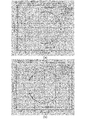
- FIG. 1A is a graph showing a simulation result of an admittance circle diagram when the excitation electrode has a one-layer structure in the crystal piece included in the crystal unit of FIG. 1.
- (B) is a graph showing the simulation result of the admittance circle diagram when the excitation electrode has a two-layer structure in the same crystal piece.
- FIG. 1 It is a schematic cross-sectional view which shows the still another embodiment of the crystal oscillator which concerns on this invention, (a) has the structure which the thickness of each of the outer edge part of an electrode and the central part of an electrode is the same, (b) is the mass in the central part of an electrode. A configuration in which a large metal film is covered with a metal film having a small mass, and (c) a configuration in which the thickness of the outer edge portion of the electrode is thicker than the thickness of the central portion of the electrode is shown.
- this structure the crystal oscillator electrode structure
- the crystal oscillator the crystal oscillator
- the crystal oscillator the crystal oscillator according to the present invention
- FIG. 1A is a schematic plan view showing an embodiment of the crystal oscillator according to the present invention
- FIG. 1B is a schematic cross-sectional view taken along the line AA of the crystal oscillator of FIG. 1A.
- the cap 50 described later is shown by a broken line.
- the crystal oscillator 1 is mounted on a predetermined oscillation circuit to generate a signal having a predetermined oscillation frequency based on an applied voltage (hereinafter referred to as "applied voltage").
- the crystal oscillator 1 is, for example, a surface mount type (SMD type) crystal oscillator.
- the crystal oscillator 1 includes a crystal piece 10, an electrode 20, a conductive adhesive 30, a housing 40, and a cap 50.
- the crystal piece 10 is excited at a predetermined frequency based on the applied voltage.
- the crystal piece 10 is, for example, an AT-cut crystal piece. Since AT cutting is a well-known technique, its description will be omitted.
- the crystal piece 10 has a rectangular shape in a plan view and a plate shape in a lateral view.
- the crystal piece 10 includes a first main surface 11 (the surface on the upper side of the paper surface in FIG. 1 (b)) and a second main surface 12 (the surface on the lower side of the paper surface in FIG. 1 (b)).
- the longitudinal direction of the crystal piece 10 is along the X-axis direction of the crystal
- the lateral direction of the crystal piece 10 is the Z'axis of the crystal (axis inclined by 35.15 ° from the Z-axis of the crystal).
- the direction perpendicular to both main surfaces 11 and 12 of the crystal piece 10 is along the Y'axis of the crystal (the axis inclined by 35.15 ° from the Y axis of the crystal).
- the first main surface 11 includes an outer edge portion 111 and a central portion 112 which is a region inside the outer edge portion 111 in a plan view.
- the central portion 112 projects in a rectangular shape above the outer edge portion 111.
- the second main surface 12 includes an outer edge portion 121 and a central portion 122 which is a region inside the outer edge portion 121 in a plan view.
- the central portion 122 projects downward in a rectangular shape from the outer edge portion 121. That is, the crystal piece 10 has a mesa-shaped structure in which the central portions 112 and 122 of both main surfaces 11 and 12 are thicker than the outer edge portions 111 and 121.
- the electrode 20 applies a predetermined voltage to the crystal piece 10.
- the structure of the electrode 20 (that is, this structure) will be described later.
- the conductive adhesive 30 electrically connects each of the pair of connection electrodes 212a and 222a, which will be described later, to the electrode pads 412 of the housing 40, which will be described later. As a result, the crystal piece 10 is mechanically fixed inside the housing 40.
- the housing 40 accommodates a crystal piece 10 having this structure, which will be described later.
- the housing 40 is a sintered body in which ceramics such as alumina are laminated.
- the housing 40 is a known housing (package) for a crystal unit.
- the housing 40 has a rectangular shape in a plan view, and has a box shape having an opening at the top.
- the housing 40 includes an electrode 41 and a step portion 42.
- the electrode 41 includes an external electrode 411 arranged on the lower surface of the bottom portion of the housing 40, and a pair of electrode pads 412 arranged on the upper surface of the bottom portion (step portion 42) of the housing 40.
- the step portion 42 is arranged on the upper surface of the bottom portion on one short side side of the housing 40.
- the cap 50 airtightly seals the opening at the top of the housing 40.
- the cap 50 is made of metal, for example.
- the electrode 20 includes a first main surface electrode 21 arranged on the first main surface 11 and a second main surface electrode 22 arranged on the second main surface 12.
- the first main surface electrode 21 includes a first excitation electrode 211 and a first extraction electrode 212.
- the first excitation electrode 211 applies an applied voltage to the crystal piece 10.
- the first excitation electrode 211 includes a first electrode portion 211a and a second electrode portion 211b.
- the first electrode portion 211a is arranged on the central portion 112 of the first main surface 11. In a plan view, the first electrode portion 211a has an area smaller than the area of the central portion 112 and is arranged inside the central portion 112.
- the second electrode portion 211b is arranged so as to be laminated on the first electrode portion 211a. In a plan view, the second electrode portion 211b has an area smaller than the area of the first electrode portion 211a and is arranged inside the first electrode portion 211a. That is, the first excitation electrode 211 has a two-layer structure composed of two electrode portions 211a and 211b that are laminated so that the area is sequentially reduced.
- the angle between the end surface (side surface) of the first electrode portion 211a and the central portion 112 of the first main surface 11 is, for example, 30 ° to 90 °.
- the angle between the end surface (side surface) of the second electrode portion 211b and the first electrode portion 211a is, for example, 30 ° to 90 °.
- the first electrode portion 211a is substantially parallel to the central portion 112 of the first main surface 11.
- the angle between the end faces of the plurality of electrode portions 211a and 211b and the virtual plane parallel to the first main surface 11 is 30 ° to 90 °.
- the angle of the end face is measured, for example, physically by a probe or optically by using transmitted light.
- the outer edge portion of the first excitation electrode 211 (the region of the first electrode portion 211a where the second electrode portion 211b is not laminated) constitutes the electrode outer edge portion in the present invention.
- the region inside the outer edge of the electrode (the region where the first electrode portion 211a and the second electrode portion 211b are laminated) constitutes the central portion of the electrode in the present invention.
- the outer edge of the electrode is composed of the first electrode portion 211a
- the central portion of the electrode is composed of the first electrode portion 211a and the second electrode portion 211b. That is, the central portion of the electrode is thicker than the outer edge portion of the electrode.
- the first extraction electrode 212 transmits the applied voltage to the first excitation electrode 211.
- the first extraction electrode 212 is connected to the first excitation electrode 211 and is arranged on the first main surface 11 so as to be drawn from the central portion 112 to the outer edge portion 111 on one short side side of the crystal piece 10. ..
- a part of the first extraction electrode 212 that is extracted (arranged) from the outer edge portion 111 constitutes a connection electrode 212a that is connected to the conductive adhesive 30.
- the first extraction electrode 212 is formed integrally with the first electrode portion 211a.
- the first extraction electrode 212 and the first electrode portion 211a include a base metal film arranged on the first main surface 11 and a metal film arranged on the base metal film.
- the second electrode portion 211b includes a base metal film arranged on the first electrode portion 211a and a metal film arranged on the base metal film.
- the base metal film is a Cr film and the metal film is an Au film.
- the second main surface electrode 22 includes a second excitation electrode 221 and a second extraction electrode 222.
- the second excitation electrode 221 applies an applied voltage to the crystal piece 10.
- the second excitation electrode 221 includes a first electrode portion 221a and a second electrode portion 221b.
- the first electrode portion 221a is arranged on the central portion 122 of the second main surface 12. In a plan view, the first electrode portion 221a has an area smaller than the area of the central portion 122 and is arranged inside the central portion 122.
- the second electrode portion 221b is arranged so as to be laminated on the first electrode portion 221a. In a plan view, the second electrode portion 221b has an area smaller than the area of the first electrode portion 221a and is arranged inside the first electrode portion 221a. That is, the second excitation electrode 221 has a two-layer structure composed of two electrode portions 221a and 221b that are laminated so that the area is sequentially reduced. In the present embodiment, the second excitation electrode 221 has a structure symmetrical with that of the first excitation electrode 211 with the crystal piece 10 interposed therebetween.
- the angle between the end surface (side surface) of the first electrode portion 221a and the central portion 122 of the second main surface 12 is, for example, 30 ° to 90 °.
- the angle between the end surface (side surface) of the second electrode portion 221b and the first electrode portion 221a is, for example, 30 ° to 90 °.
- the first electrode portion 221a is substantially parallel to the central portion 122 of the second main surface 12. In other words, the angle between the end faces of the plurality of electrode portions 221a and 221b and the virtual plane parallel to the second main surface 12 is 30 ° to 90 °.
- the outer edge portion of the second excitation electrode 221 (the region of the first electrode portion 221a in which the second electrode portion 221b is not laminated) constitutes the electrode outer edge portion in the present invention.
- the region inside the outer edge of the electrode (the region where the first electrode portion 221a and the second electrode portion 221b are laminated) constitutes the central portion of the electrode in the present invention.
- the outer edge of the electrode is composed of the first electrode portion 221a
- the central portion of the electrode is composed of the first electrode portion 221a and the second electrode portion 221b. That is, the central portion of the electrode is thicker than the outer edge portion of the electrode.
- the second extraction electrode 222 transmits the applied voltage to the second excitation electrode 221.
- the second extraction electrode 222 is connected to the second excitation electrode 221 and is arranged on the second main surface 12 so as to be drawn from the central portion 122 to the outer edge portion 121 on one short side side of the crystal piece 10. ..
- a part of the second extraction electrode 222 that is extracted (arranged) from the outer edge portion 121 constitutes a connection electrode 222a that is connected to the conductive adhesive 30.
- the second extraction electrode 222 is formed integrally with the first electrode portion 221a.
- the second extraction electrode 222 and the first electrode portion 221a include a base metal film arranged on the second main surface 12 and a metal film arranged on the base metal film.
- the second electrode portion 221b includes a base metal film arranged on the first electrode portion 221a and a metal film arranged on the base metal film.
- the base metal film is a Cr film and the metal film is an Au film.
- Each of the first main surface electrode 21 and the second main surface electrode 22 is formed by, for example, a photolithography process. That is, for example, after the base metal film and the metal film are formed on the crystal piece 10 by vapor deposition or the like, the second electrode portions 211b and 221b are masked by the resist, and then the metal film and the base metal on the upper layer side are formed. The film and the film are removed by etching. Next, with the first electrode portions 211a and 221a, the first extraction electrode 212, and the second extraction electrode 222 masked, the metal film on the lower layer side and the base metal film are removed by etching.
- the base metal film and the metal film on the upper layer side are vapor-deposited in a state where the portion other than the second electrode portion is masked by the resist. You may. In this case, both the underlying metal film and the metal film other than the second electrode portion are removed together with the resist.
- the base metal film and the metal film on the upper layer side are formed in a state where the parts other than the second electrode portion are masked by a metal mask or the like. It may be vapor-deposited.
- FIG. 2 is a graph showing an example of the relationship between the electrode area ratio and the CI value when the area of the first electrode portion 211a is fixed and the area of the second electrode portion 211b is changed.
- the horizontal axis in the figure shows the area ratio of the second electrode portion 211b to the area of the first electrode portion 211a (area of the second electrode portion 211b / area of the first electrode portion 211a).
- the vertical axis of the figure shows the CI value. As shown in FIG. 2, the CI value decreases when the area ratio is about 83% to 95%, and particularly when the area ratio is about 83% to 90%.
- FIG. 3A is a graph showing a simulation result of an admittance circle diagram when the excitation electrode has a one-layer structure in a crystal piece equivalent to the crystal piece 10 of the present embodiment
- FIG. 3B is a graph. It is a graph which shows the simulation result of the admittance circle diagram in this embodiment (the excitation electrode has a two-layer structure).
- the CI value (about 10 ⁇ ) when the excitation electrode has a two-layer structure is significantly reduced as compared with the CI value (about 70 ⁇ ) when the excitation electrode has a one-layer structure. ..
- FIG. 4 is a graph showing the magnitude of displacement of the crystal piece 10 in the longitudinal direction of the crystal piece 10 when the voltage applied to the crystal piece 10 is constant.
- the horizontal axis in the figure indicates the position of the crystal piece 10 in the longitudinal direction (X-axis direction in the axial direction of the crystal).
- the vertical axis in the figure shows the magnitude of displacement in the X-axis direction.
- “L1” in the figure shows the displacement when the excitation electrode has a one-layer structure
- “L2” in the figure shows the displacement when the excitation electrode has a two-layer structure.
- the displacement when the excitation electrode has a two-layer structure is about two to three times larger than the displacement when the excitation electrode has the same one-layer structure.
- the difference in displacement between the two structures increases from the end to the center in the X-axis direction. This indicates that the vibration energy of the main vibration is concentrated in the central region of the crystal piece 10 (the region between the central portions 112 and 122 of both main surfaces 11 and 12), and the energy is confined in the central region. ..
- each of the first excitation electrode 211 and the second excitation electrode 221 has a two-layer structure in which the area becomes smaller as it becomes an upper layer, so that the vibration energy of the main vibration is concentrated in the central region of the crystal piece 10. However, the vibration energy is confined in the central region. As a result, the equivalent series resistance (CI) value of the crystal piece 10 is reduced.
- Crystal oscillator ⁇ Next, an embodiment of the crystal oscillator according to the present invention will be described. In the embodiments described below, the description of the members common to the embodiments described above will be omitted.
- FIG. 5 is a schematic cross-sectional view showing an embodiment of the crystal oscillator according to the present invention.
- the crystal oscillator 100 is, for example, a temperature-compensated crystal oscillator (TCXO).
- the crystal oscillator 100 is, for example, an SMD type crystal oscillator.
- the crystal oscillator 100 includes the above-mentioned crystal piece 10, an electrode 20, a conductive adhesive 30, a cap 50, a housing 40A, and a circuit 60A.
- the housing 40A accommodates the crystal piece 10 and the circuit 60A.
- the housing 40A is a sintered body in which ceramics such as alumina are laminated.
- the housing 40A is a housing (package) of a known crystal oscillator.
- the housing 40A has a rectangular shape in a plan view and a box shape having an opening at the top.
- the housing 40A includes an electrode (not shown), a step portion 42, and a circuit accommodating portion 43A.
- the circuit accommodating unit 43A accommodates the circuit 60A.
- the circuit accommodating portion 43A is arranged in the central portion of the bottom portion of the housing 40A.
- the circuit 60A controls the oscillation frequency of the crystal piece 10 (crystal oscillator 1).
- the circuit 60A is, for example, a known temperature compensation circuit.
- the present structure has a two-layer structure in which the first excitation electrode 211 and the second excitation electrode 221 each have a smaller area as they become upper layers. Therefore, in this structure, the vibration energy of the main vibration is concentrated in the central region of the crystal piece 10, and the vibration energy is confined in the central region. As a result, the CI value of the crystal piece 10 is reduced. As described above, the CI value of this structure, the crystal oscillator 1 having this structure, and the crystal oscillator 100 can be reduced without requiring precise processing of the crystal piece 10.
- the absolute value of the variation in the CI value becomes smaller. That is, for example, the average CI value increased by 50% with respect to the average CI value of 100 ⁇ is 150 ⁇ , but the average CI value increased by 50% with respect to the average CI value of 10 ⁇ is 15 ⁇ . Further, for example, the CI value increased by 50 ⁇ with respect to the CI value of 100 ⁇ is 150 ⁇ , but the CI value increased by 50 ⁇ with respect to the CI value of 10 ⁇ is 60 ⁇ . In this way, even if the CI value varies, the CI value tends to be within the standard. As a result, the productivity (yield) of each of the crystal oscillator 1 and the crystal oscillator 100 having this structure is improved. Further, in this case, by reducing the CI value according to the present invention, the etching amount of the outer edge portions 111 and 121 of the crystal piece 10 is reduced. As a result, the productivity (yield) of the crystal piece 10 is improved.
- the vibration energy of the main vibration is confined in the central region of the crystal piece 10, so that the end portion of the crystal piece 10, that is, the connection electrodes 212a and 222a are arranged.
- the influence of the coupling vibration on the outer edge portion 111 of 10 is suppressed. Therefore, the influence of the conductive adhesive 30 on the main vibration is suppressed.
- the productivity (yield) of each of the crystal oscillator 1 and the crystal oscillator 100 having this structure is improved.
- the crystal oscillator 100 using the crystal oscillator 1 having this structure enables low excitation operation when incorporated in an oscillation circuit, and contributes to stabilization of oscillation. do.
- the crystal piece in the present invention may be excited by a thickness sliding vibration as the main vibration, and the cutting of the crystal piece in the present invention is not limited to the AT cut. That is, for example, the crystal piece cut in the present invention may be a BT cut, an SC cut, or an IT cut.
- the crystal piece in the present invention is not limited to the mesa type. That is, for example, the crystal piece in the present invention may have any of a flat plate type, a bevel type, an inverted mesa type, a convex type, and a plano convex type.
- the bevel amount is reduced in the bevel type, and the etching amount of the central concave portion of the crystal piece is reduced in the inverted mesa type. As a result, the productivity (yield) of the crystal piece is improved.
- FIG. 6 (a)-(c) are schematic cross-sectional views showing another embodiment of the crystal unit according to the present invention.
- the figure shows only the cross sections of the crystal piece and the electrode for convenience of explanation.
- FIG. 3A shows a flat plate type crystal piece
- FIG. 2B shows a bevel type crystal piece
- FIG. 6C shows an inverted mesa type crystal piece.
- the length of the long side (side along the X-axis direction) of each crystal piece in the present invention is preferably 2 mm or less. According to this configuration, this structure reduces the CI value as compared with other structures (for example, the shape of the crystal piece, the thickness / position of the electrode, etc.). That is, in this structure, the smaller the crystal piece, the lower the CI value than other structures.
- the crystal pieces in the present invention may be collectively formed by a photolithography step, or may be individually formed by a method such as polishing, cutting, or surface etching.
- the crystal piece in the present invention may be excited in the vibration mode of the fundamental wave mode, or may be excited in the vibration mode of the high-order (third-order) overtone mode.
- each of the first excitation electrode and the second excitation electrode in the present invention may be arranged on both main surfaces and may be composed of a plurality of electrode portions laminated so that the areas are sequentially reduced, and the two-layer structure may be formed.
- the first excitation electrode and the second excitation electrode in the present invention are respectively arranged in a laminated manner on the second electrode portion, and include a third electrode portion having an area smaller than the area of the second electrode portion. May be good.
- the number of layers of the first excitation electrode may be different from the number of layers of the second excitation electrode.
- the second excitation electrode in the present invention may have a structure asymmetrical with that of the first excitation electrode with the crystal piece interposed therebetween. That is, for example, the second excitation electrode in the present invention may be arranged so as to be displaced in the X-axis direction and / or the Z'axis direction with respect to the first excitation electrode in a plan view.
- first electrode portion and the second electrode portion in the present invention may be integrally configured. That is, for example, the first electrode portion and the second electrode portion in the present invention may be composed of one layer of the base metal film and the metal film. In this case, the outer edge portion of the electrode may be formed, for example, by removing the outer edge portion of the one-layer metal film.
- the thickness of the first electrode portion and the thickness of the second electrode portion in the present invention may be the same or different.
- the thickness of each electrode portion is calculated based on, for example, the frequency of the crystal piece before and after the vapor deposition. Further, the thickness of each electrode portion may be physically measured by a probe, or may be optically measured by using transmitted light, for example.
- the base metal film in the present invention may be a metal film having an affinity for each of the crystal piece and the metal film, and is not limited to the Cr film. That is, for example, the base metal film in the present invention may contain at least one metal among Cr, Ni and W.
- the metal film in the present invention is not limited to the Au film as long as it is a metal film capable of supplying an applied voltage that can be excited by the crystal. That is, for example, the metal film in the present invention may contain at least one metal among Au, Ag, Cu, Al, W, Ni, and Mg.
- each of the first excitation electrode and the second excitation electrode in the present invention has an outer edge portion of the electrode and a region inside the outer edge portion of the electrode in a plan view, and has a larger mass than the metal constituting the outer edge portion of the electrode. It may be composed of a central portion of the electrode containing the metal having the metal. That is, for example, the outer edge portion of the electrode may be composed of an Ag or Al film, and the central portion of the electrode may be composed of an Au film. In this configuration, the mass of the central portion of the electrode in the uniaxial direction (for example, the X-axis direction) may be larger than the mass of the outer edge portion of the electrode.
- the thickness of the central portion of the electrode may be the same as the thickness of the outer edge portion of the electrode, or may be thinner than the thickness of the outer edge portion of the electrode.
- a metal film having a large mass for example, Au film
- a metal film having a small mass for example, Al film.
- FIG. 7 (a)-(c) are schematic cross-sectional views showing still another embodiment of the crystal unit according to the present invention.
- the figure shows only the cross sections of the crystal piece and the electrode for convenience of explanation.
- the black-painted electrode in the figure is composed of a metal having a larger mass than the white electrode.
- FIG. 3A shows a configuration in which the outer edge of the electrode and the central portion of the electrode have the same thickness
- FIG. (c) shows a configuration in which the thickness of the outer edge portion of the electrode is thicker than the thickness of the central portion of the electrode.
- each electrode portion in the present invention may be a curved surface.
- one side of the four sides of the second electrode in the present invention may overlap with one side of the four sides of the first electrode.
- the crystal oscillator according to the present invention is not limited to the temperature-compensated crystal oscillator. That is, for example, the crystal oscillator according to the present invention may be a voltage-controlled crystal oscillator (VCXO), a crystal oscillator with a constant temperature bath (OCXO), or a packaged crystal oscillator (SPXO).
- VCXO voltage-controlled crystal oscillator
- OCXO crystal oscillator with a constant temperature bath
- SPXO packaged crystal oscillator
- Crystal oscillator 10 Crystal piece 11 First main surface 12 Second main surface 21 First main surface electrode 211 First excitation electrode 211a First electrode portion 211b Second electrode portion 22 Second main surface electrode 221 Second excitation electrode 221a 1st electrode part 221b 2nd electrode part 100 Crystal oscillator
Landscapes
- Physics & Mathematics (AREA)
- Acoustics & Sound (AREA)
- Chemical & Material Sciences (AREA)
- Engineering & Computer Science (AREA)
- Ceramic Engineering (AREA)
- Piezo-Electric Or Mechanical Vibrators, Or Delay Or Filter Circuits (AREA)
Priority Applications (2)
| Application Number | Priority Date | Filing Date | Title |
|---|---|---|---|
| CN202080096715.5A CN115136494A (zh) | 2020-03-18 | 2020-12-28 | 晶体振子的电极结构、晶体振子和晶体振荡器 |
| US17/906,267 US12512814B2 (en) | 2020-03-18 | 2020-12-28 | Electrode structure of crystal unit, crystal unit, and crystal oscillator |
Applications Claiming Priority (2)
| Application Number | Priority Date | Filing Date | Title |
|---|---|---|---|
| JP2020-047607 | 2020-03-18 | ||
| JP2020047607A JP7311152B2 (ja) | 2020-03-18 | 2020-03-18 | 水晶振動子の電極構造、水晶振動子、水晶発振器 |
Publications (1)
| Publication Number | Publication Date |
|---|---|
| WO2021186839A1 true WO2021186839A1 (ja) | 2021-09-23 |
Family
ID=77771144
Family Applications (1)
| Application Number | Title | Priority Date | Filing Date |
|---|---|---|---|
| PCT/JP2020/049056 Ceased WO2021186839A1 (ja) | 2020-03-18 | 2020-12-28 | 水晶振動子の電極構造、水晶振動子、水晶発振器 |
Country Status (5)
| Country | Link |
|---|---|
| US (1) | US12512814B2 (https=) |
| JP (1) | JP7311152B2 (https=) |
| CN (1) | CN115136494A (https=) |
| TW (1) | TWI828973B (https=) |
| WO (1) | WO2021186839A1 (https=) |
Families Citing this family (1)
| Publication number | Priority date | Publication date | Assignee | Title |
|---|---|---|---|---|
| WO2024214335A1 (ja) * | 2023-04-14 | 2024-10-17 | 株式会社村田製作所 | 圧電振動素子 |
Citations (6)
| Publication number | Priority date | Publication date | Assignee | Title |
|---|---|---|---|---|
| JP2003273682A (ja) * | 2002-03-15 | 2003-09-26 | Seiko Epson Corp | 圧電振動片の周波数調整方法、圧電振動片および圧電デバイス |
| JP2005159717A (ja) * | 2003-11-26 | 2005-06-16 | Toyo Commun Equip Co Ltd | 圧電振動子とその製造方法 |
| JP2005318477A (ja) * | 2004-04-30 | 2005-11-10 | Seiko Epson Corp | 圧電振動片、その電極形成方法、及び圧電デバイス |
| JP2013255052A (ja) * | 2012-06-06 | 2013-12-19 | Seiko Epson Corp | 振動素子、振動子、電子デバイス、電子機器、移動体および振動素子の製造方法 |
| JP2017152994A (ja) * | 2016-02-26 | 2017-08-31 | 京セラ株式会社 | 水晶素子および水晶デバイス |
| JP2018117198A (ja) * | 2017-01-17 | 2018-07-26 | 日本電波工業株式会社 | 圧電振動片及び圧電デバイス |
Family Cites Families (52)
| Publication number | Priority date | Publication date | Assignee | Title |
|---|---|---|---|---|
| JP3640497B2 (ja) * | 1997-03-05 | 2005-04-20 | パイオニア株式会社 | 収差補正装置及び情報記録媒体再生装置 |
| JP3731348B2 (ja) * | 1998-06-09 | 2006-01-05 | 松下電器産業株式会社 | 圧電振動子 |
| JP3775965B2 (ja) * | 2000-02-07 | 2006-05-17 | パイオニア株式会社 | 光学式情報再生装置 |
| KR100754158B1 (ko) * | 2000-12-08 | 2007-09-03 | 삼성전자주식회사 | 구면수차 검출 및/또는 보정 가능한 광픽업장치 |
| US20030048041A1 (en) * | 2001-09-07 | 2003-03-13 | Hiroyuki Kita | Piezoelectric thin-film element and a manufacturing method thereof |
| JP4036149B2 (ja) | 2003-07-03 | 2008-01-23 | セイコーエプソン株式会社 | 圧電デバイスのリーク検出方法 |
| JP4459685B2 (ja) * | 2004-03-31 | 2010-04-28 | 富士通株式会社 | 液晶表示装置 |
| US7764329B2 (en) * | 2005-12-02 | 2010-07-27 | Au Optronics Corp. | MVA LCD device and pixel circuit thereof |
| JP2009110556A (ja) * | 2006-02-14 | 2009-05-21 | Panasonic Corp | 光学ヘッドおよび光情報処理装置 |
| JP4665849B2 (ja) | 2006-06-23 | 2011-04-06 | 株式会社大真空 | 圧電振動デバイスの製造方法 |
| TWI364734B (en) * | 2006-06-30 | 2012-05-21 | Chimei Innolux Corp | Liquid crystal display panel, driving method and liquid crystal displayer |
| JP4687985B2 (ja) | 2006-08-10 | 2011-05-25 | 株式会社大真空 | 圧電振動デバイスの周波数調整方法 |
| KR101404544B1 (ko) * | 2007-08-07 | 2014-06-10 | 삼성디스플레이 주식회사 | 액정 표시 장치 |
| TWI339304B (en) * | 2007-10-16 | 2011-03-21 | Au Optronics Corp | Pixel structure, driving method thereof and pixel array structure |
| US20120057118A1 (en) * | 2009-05-28 | 2012-03-08 | Katsuhiko Morishita | Liquid crystal display device |
| JP5589167B2 (ja) * | 2010-11-19 | 2014-09-17 | セイコーエプソン株式会社 | 圧電振動片および圧電振動子 |
| CN102684636B (zh) * | 2011-03-09 | 2015-12-16 | 精工爱普生株式会社 | 振动元件、振子、振荡器以及电子设备 |
| JP5708089B2 (ja) * | 2011-03-18 | 2015-04-30 | セイコーエプソン株式会社 | 圧電振動素子、圧電振動子、圧電発振器及び電子デバイス |
| JP2013021667A (ja) | 2011-03-23 | 2013-01-31 | Nippon Dempa Kogyo Co Ltd | 水晶デバイス |
| CN102957394B (zh) * | 2011-08-18 | 2016-12-21 | 精工爱普生株式会社 | 振动元件、振子、电子装置、电子设备、移动体及振动元件的制造方法 |
| US8970316B2 (en) * | 2011-08-19 | 2015-03-03 | Seiko Epson Corporation | Resonating element, resonator, electronic device, electronic apparatus, and mobile object |
| JP5943186B2 (ja) * | 2012-03-19 | 2016-06-29 | セイコーエプソン株式会社 | 振動片、振動子、電子デバイス、および電子機器 |
| JP5943187B2 (ja) * | 2012-03-21 | 2016-06-29 | セイコーエプソン株式会社 | 振動素子、振動子、電子デバイス、および電子機器 |
| CN103843249B (zh) * | 2012-04-04 | 2016-01-20 | 株式会社村田制作所 | 水晶振动装置 |
| JP6083144B2 (ja) | 2012-07-27 | 2017-02-22 | セイコーエプソン株式会社 | 振動片、振動素子、振動子、電子デバイス、電子機器、移動体及び振動片の製造方法 |
| JP2015019240A (ja) * | 2013-07-11 | 2015-01-29 | 日本電波工業株式会社 | 圧電振動片、圧電振動片の製造方法、圧電デバイス、及び圧電デバイスの製造方法 |
| JP2016019225A (ja) | 2014-07-10 | 2016-02-01 | 富士通株式会社 | 水晶振動子 |
| JP6390836B2 (ja) * | 2014-07-31 | 2018-09-19 | セイコーエプソン株式会社 | 振動片、振動子、振動デバイス、発振器、電子機器、および移動体 |
| KR20160032600A (ko) * | 2014-09-16 | 2016-03-24 | 삼성전기주식회사 | 압전 진동편, 그 제조방법 및 압전 진동자 |
| JP6500915B2 (ja) * | 2015-01-29 | 2019-04-17 | 株式会社大真空 | 水晶振動板、及び水晶振動デバイス |
| JP2016140023A (ja) * | 2015-01-29 | 2016-08-04 | セイコーエプソン株式会社 | 振動片、振動子、振動デバイス、発振器、電子機器、および移動体 |
| CN107408935B (zh) * | 2015-03-03 | 2018-11-09 | 株式会社村田制作所 | 晶体振子 |
| JP6552225B2 (ja) | 2015-03-12 | 2019-07-31 | エスアイアイ・クリスタルテクノロジー株式会社 | 圧電振動片及び圧電振動子 |
| JP6591194B2 (ja) * | 2015-05-15 | 2019-10-16 | 株式会社ジャパンディスプレイ | 液晶表示装置 |
| CN107636963B (zh) * | 2015-06-12 | 2020-07-28 | 株式会社村田制作所 | 石英片以及石英振子 |
| WO2016199918A1 (ja) * | 2015-06-12 | 2016-12-15 | 株式会社村田製作所 | 水晶片及び水晶振動子 |
| CN107636962B (zh) * | 2015-06-12 | 2020-07-31 | 株式会社村田制作所 | 石英片以及石英振子 |
| WO2017006941A1 (ja) * | 2015-07-09 | 2017-01-12 | 株式会社村田製作所 | 水晶振動片及び水晶振動子 |
| CN107852147B (zh) * | 2015-09-01 | 2021-02-05 | 株式会社村田制作所 | 水晶片以及水晶振子 |
| CN108028638B (zh) * | 2015-09-25 | 2021-01-05 | 株式会社村田制作所 | 水晶片以及水晶振子 |
| CN108028639B (zh) * | 2015-09-28 | 2021-01-08 | 株式会社村田制作所 | 晶体片以及晶体振子 |
| WO2017057167A1 (ja) * | 2015-09-30 | 2017-04-06 | 株式会社村田製作所 | 水晶片及び水晶振動子 |
| CN108141194B (zh) * | 2015-10-02 | 2021-07-06 | 株式会社村田制作所 | 晶体片以及晶体振子 |
| JP6579344B2 (ja) * | 2016-01-21 | 2019-09-25 | 株式会社村田製作所 | 水晶振動子及びその製造方法 |
| JP2017192032A (ja) | 2016-04-13 | 2017-10-19 | 日本電波工業株式会社 | 水晶振動子 |
| CN109690940B (zh) * | 2016-09-08 | 2023-03-14 | 株式会社村田制作所 | 水晶振子及其制造方法 |
| JP6807046B2 (ja) | 2016-09-08 | 2021-01-06 | 株式会社村田製作所 | 水晶振動素子及びその製造方法並びに水晶振動子及びその製造方法 |
| JP6910134B2 (ja) * | 2016-11-30 | 2021-07-28 | 京セラ株式会社 | 圧電振動素子及び圧電振動デバイス |
| US20180241371A1 (en) | 2017-02-21 | 2018-08-23 | Nihon Dempa Kogyo Co., Ltd. | Piezoelectric device |
| WO2018212150A1 (ja) * | 2017-05-15 | 2018-11-22 | 株式会社村田製作所 | 水晶振動素子及び水晶振動子並びにそれらの製造方法 |
| JP6970391B2 (ja) * | 2017-09-22 | 2021-11-24 | 株式会社村田製作所 | 圧電振動素子の製造方法及び圧電振動子の製造方法 |
| JP7259940B2 (ja) * | 2019-03-28 | 2023-04-18 | 株式会社村田製作所 | 圧電振動子とその製造方法 |
-
2020
- 2020-03-18 JP JP2020047607A patent/JP7311152B2/ja active Active
- 2020-12-28 US US17/906,267 patent/US12512814B2/en active Active
- 2020-12-28 CN CN202080096715.5A patent/CN115136494A/zh active Pending
- 2020-12-28 WO PCT/JP2020/049056 patent/WO2021186839A1/ja not_active Ceased
-
2021
- 2021-03-10 TW TW110108543A patent/TWI828973B/zh active
Patent Citations (6)
| Publication number | Priority date | Publication date | Assignee | Title |
|---|---|---|---|---|
| JP2003273682A (ja) * | 2002-03-15 | 2003-09-26 | Seiko Epson Corp | 圧電振動片の周波数調整方法、圧電振動片および圧電デバイス |
| JP2005159717A (ja) * | 2003-11-26 | 2005-06-16 | Toyo Commun Equip Co Ltd | 圧電振動子とその製造方法 |
| JP2005318477A (ja) * | 2004-04-30 | 2005-11-10 | Seiko Epson Corp | 圧電振動片、その電極形成方法、及び圧電デバイス |
| JP2013255052A (ja) * | 2012-06-06 | 2013-12-19 | Seiko Epson Corp | 振動素子、振動子、電子デバイス、電子機器、移動体および振動素子の製造方法 |
| JP2017152994A (ja) * | 2016-02-26 | 2017-08-31 | 京セラ株式会社 | 水晶素子および水晶デバイス |
| JP2018117198A (ja) * | 2017-01-17 | 2018-07-26 | 日本電波工業株式会社 | 圧電振動片及び圧電デバイス |
Also Published As
| Publication number | Publication date |
|---|---|
| JP7311152B2 (ja) | 2023-07-19 |
| TWI828973B (zh) | 2024-01-11 |
| CN115136494A (zh) | 2022-09-30 |
| US20230130678A1 (en) | 2023-04-27 |
| TW202137698A (zh) | 2021-10-01 |
| JP2021150761A (ja) | 2021-09-27 |
| US12512814B2 (en) | 2025-12-30 |
Similar Documents
| Publication | Publication Date | Title |
|---|---|---|
| JP5632627B2 (ja) | 水晶振動片 | |
| JP5912557B2 (ja) | 音叉型圧電振動片及び圧電デバイス | |
| US7368861B2 (en) | Piezoelectric resonator element and piezoelectric device | |
| JP2010098531A (ja) | 圧電振動片および圧電デバイス | |
| JP5088613B2 (ja) | 振動デバイスの周波数調整方法、並びに振動デバイスおよび電子デバイス | |
| JP2013042440A (ja) | 圧電振動素子、圧電振動子、電子デバイス、及び電子機器 | |
| JP4301201B2 (ja) | 圧電発振器 | |
| WO2021186839A1 (ja) | 水晶振動子の電極構造、水晶振動子、水晶発振器 | |
| JP2010004456A (ja) | 圧電振動片および圧電デバイス | |
| JP5824958B2 (ja) | 振動素子、振動子、電子デバイス、及び電子機器 | |
| CN109891745B (zh) | 音叉型振子及音叉型振子的制造方法 | |
| JP4558433B2 (ja) | 水晶振動子 | |
| CN101478297B (zh) | 用于表面安装的石英晶体器件 | |
| EP4311108A1 (en) | Quartz resonator and method for producing same | |
| JP2016040950A (ja) | 振動素子、振動子、電子デバイス、及び電子機器 | |
| JP5495080B2 (ja) | 振動デバイスの周波数調整方法、並びに振動デバイス、および電子デバイス | |
| JP2013026761A (ja) | 水晶発振器 | |
| JP5872660B2 (ja) | 水晶振動片 | |
| JP2021068955A (ja) | 音叉型圧電振動片および当該音叉型圧電振動片を用いた音叉型圧電振動子 | |
| JP7725962B2 (ja) | 水晶振動板および水晶振動デバイス | |
| JP7423231B2 (ja) | 圧電振動片の製造方法、圧電振動片および圧電振動子 | |
| JP2026042083A (ja) | 水晶振動板および水晶振動デバイス | |
| JP2018037896A (ja) | 音叉型圧電振動片および当該音叉型圧電振動片を用いた音叉型圧電振動子 | |
| JP2017157934A (ja) | 音叉型圧電振動片および当該音叉型圧電振動片を用いた圧電デバイス | |
| JP2007028271A (ja) | 圧電振動子の周波数調整方法および圧電振動子 |
Legal Events
| Date | Code | Title | Description |
|---|---|---|---|
| 121 | Ep: the epo has been informed by wipo that ep was designated in this application |
Ref document number: 20926230 Country of ref document: EP Kind code of ref document: A1 |
|
| NENP | Non-entry into the national phase |
Ref country code: DE |
|
| 122 | Ep: pct application non-entry in european phase |
Ref document number: 20926230 Country of ref document: EP Kind code of ref document: A1 |
|
| WWG | Wipo information: grant in national office |
Ref document number: 17906267 Country of ref document: US |