WO2021140898A1 - 窒化物半導体装置 - Google Patents
窒化物半導体装置 Download PDFInfo
- Publication number
- WO2021140898A1 WO2021140898A1 PCT/JP2020/047685 JP2020047685W WO2021140898A1 WO 2021140898 A1 WO2021140898 A1 WO 2021140898A1 JP 2020047685 W JP2020047685 W JP 2020047685W WO 2021140898 A1 WO2021140898 A1 WO 2021140898A1
- Authority
- WO
- WIPO (PCT)
- Prior art keywords
- layer
- nitride semiconductor
- electron
- opening
- semiconductor device
- Prior art date
- Legal status (The legal status is an assumption and is not a legal conclusion. Google has not performed a legal analysis and makes no representation as to the accuracy of the status listed.)
- Ceased
Links
Images


Classifications
-
- H—ELECTRICITY
- H10—SEMICONDUCTOR DEVICES; ELECTRIC SOLID-STATE DEVICES NOT OTHERWISE PROVIDED FOR
- H10D—INORGANIC ELECTRIC SEMICONDUCTOR DEVICES
- H10D30/00—Field-effect transistors [FET]
- H10D30/40—FETs having zero-dimensional [0D], one-dimensional [1D] or two-dimensional [2D] charge carrier gas channels
- H10D30/47—FETs having zero-dimensional [0D], one-dimensional [1D] or two-dimensional [2D] charge carrier gas channels having two-dimensional [2D] charge carrier gas channels, e.g. nanoribbon FETs or high electron mobility transistors [HEMT]
- H10D30/471—High electron mobility transistors [HEMT] or high hole mobility transistors [HHMT]
- H10D30/477—Vertical HEMTs or vertical HHMTs
-
- H—ELECTRICITY
- H10—SEMICONDUCTOR DEVICES; ELECTRIC SOLID-STATE DEVICES NOT OTHERWISE PROVIDED FOR
- H10D—INORGANIC ELECTRIC SEMICONDUCTOR DEVICES
- H10D30/00—Field-effect transistors [FET]
- H10D30/01—Manufacture or treatment
- H10D30/015—Manufacture or treatment of FETs having heterojunction interface channels or heterojunction gate electrodes, e.g. HEMT
-
- H—ELECTRICITY
- H10—SEMICONDUCTOR DEVICES; ELECTRIC SOLID-STATE DEVICES NOT OTHERWISE PROVIDED FOR
- H10D—INORGANIC ELECTRIC SEMICONDUCTOR DEVICES
- H10D30/00—Field-effect transistors [FET]
- H10D30/01—Manufacture or treatment
- H10D30/051—Manufacture or treatment of FETs having PN junction gates
-
- H—ELECTRICITY
- H10—SEMICONDUCTOR DEVICES; ELECTRIC SOLID-STATE DEVICES NOT OTHERWISE PROVIDED FOR
- H10D—INORGANIC ELECTRIC SEMICONDUCTOR DEVICES
- H10D30/00—Field-effect transistors [FET]
- H10D30/01—Manufacture or treatment
- H10D30/061—Manufacture or treatment of FETs having Schottky gates
-
- H—ELECTRICITY
- H10—SEMICONDUCTOR DEVICES; ELECTRIC SOLID-STATE DEVICES NOT OTHERWISE PROVIDED FOR
- H10D—INORGANIC ELECTRIC SEMICONDUCTOR DEVICES
- H10D30/00—Field-effect transistors [FET]
- H10D30/40—FETs having zero-dimensional [0D], one-dimensional [1D] or two-dimensional [2D] charge carrier gas channels
- H10D30/47—FETs having zero-dimensional [0D], one-dimensional [1D] or two-dimensional [2D] charge carrier gas channels having two-dimensional [2D] charge carrier gas channels, e.g. nanoribbon FETs or high electron mobility transistors [HEMT]
- H10D30/471—High electron mobility transistors [HEMT] or high hole mobility transistors [HHMT]
- H10D30/478—High electron mobility transistors [HEMT] or high hole mobility transistors [HHMT] the 2D charge carrier gas being at least partially not parallel to a main surface of the semiconductor body
-
- H—ELECTRICITY
- H10—SEMICONDUCTOR DEVICES; ELECTRIC SOLID-STATE DEVICES NOT OTHERWISE PROVIDED FOR
- H10D—INORGANIC ELECTRIC SEMICONDUCTOR DEVICES
- H10D30/00—Field-effect transistors [FET]
- H10D30/80—FETs having rectifying junction gate electrodes
- H10D30/83—FETs having PN junction gate electrodes
-
- H—ELECTRICITY
- H10—SEMICONDUCTOR DEVICES; ELECTRIC SOLID-STATE DEVICES NOT OTHERWISE PROVIDED FOR
- H10D—INORGANIC ELECTRIC SEMICONDUCTOR DEVICES
- H10D30/00—Field-effect transistors [FET]
- H10D30/80—FETs having rectifying junction gate electrodes
- H10D30/87—FETs having Schottky gate electrodes, e.g. metal-semiconductor FETs [MESFET]
-
- H—ELECTRICITY
- H10—SEMICONDUCTOR DEVICES; ELECTRIC SOLID-STATE DEVICES NOT OTHERWISE PROVIDED FOR
- H10D—INORGANIC ELECTRIC SEMICONDUCTOR DEVICES
- H10D62/00—Semiconductor bodies, or regions thereof, of devices having potential barriers
- H10D62/50—Physical imperfections
- H10D62/53—Physical imperfections the imperfections being within the semiconductor body
-
- H—ELECTRICITY
- H10—SEMICONDUCTOR DEVICES; ELECTRIC SOLID-STATE DEVICES NOT OTHERWISE PROVIDED FOR
- H10D—INORGANIC ELECTRIC SEMICONDUCTOR DEVICES
- H10D62/00—Semiconductor bodies, or regions thereof, of devices having potential barriers
- H10D62/80—Semiconductor bodies, or regions thereof, of devices having potential barriers characterised by the materials
- H10D62/83—Semiconductor bodies, or regions thereof, of devices having potential barriers characterised by the materials being Group IV materials, e.g. B-doped Si or undoped Ge
-
- H—ELECTRICITY
- H10—SEMICONDUCTOR DEVICES; ELECTRIC SOLID-STATE DEVICES NOT OTHERWISE PROVIDED FOR
- H10D—INORGANIC ELECTRIC SEMICONDUCTOR DEVICES
- H10D64/00—Electrodes of devices having potential barriers
- H10D64/20—Electrodes characterised by their shapes, relative sizes or dispositions
- H10D64/23—Electrodes carrying the current to be rectified, amplified, oscillated or switched, e.g. sources, drains, anodes or cathodes
- H10D64/251—Source or drain electrodes for field-effect devices
- H10D64/256—Source or drain electrodes for field-effect devices for lateral devices wherein the source or drain electrodes are recessed in semiconductor bodies
-
- H—ELECTRICITY
- H10—SEMICONDUCTOR DEVICES; ELECTRIC SOLID-STATE DEVICES NOT OTHERWISE PROVIDED FOR
- H10D—INORGANIC ELECTRIC SEMICONDUCTOR DEVICES
- H10D64/00—Electrodes of devices having potential barriers
- H10D64/20—Electrodes characterised by their shapes, relative sizes or dispositions
- H10D64/27—Electrodes not carrying the current to be rectified, amplified, oscillated or switched, e.g. gates
- H10D64/311—Gate electrodes for field-effect devices
- H10D64/411—Gate electrodes for field-effect devices for FETs
-
- H—ELECTRICITY
- H10—SEMICONDUCTOR DEVICES; ELECTRIC SOLID-STATE DEVICES NOT OTHERWISE PROVIDED FOR
- H10D—INORGANIC ELECTRIC SEMICONDUCTOR DEVICES
- H10D62/00—Semiconductor bodies, or regions thereof, of devices having potential barriers
- H10D62/80—Semiconductor bodies, or regions thereof, of devices having potential barriers characterised by the materials
- H10D62/85—Semiconductor bodies, or regions thereof, of devices having potential barriers characterised by the materials being Group III-V materials, e.g. GaAs
- H10D62/8503—Nitride Group III-V materials, e.g. AlN or GaN
Definitions
- This disclosure relates to a nitride semiconductor device.
- Nitride semiconductors such as GaN (gallium nitride) are wide-gap semiconductors with a large bandgap, have a large insulation breakdown electric field, and have a higher electron saturation drift rate than GaAs (gallium arsenide) semiconductors or Si (silicon) semiconductors. It has the feature of being large. Therefore, research and development of a power transistor using a nitride semiconductor, which is advantageous for high output and high withstand voltage, is being carried out.
- GaN gallium nitride
- Patent Document 1 discloses a semiconductor device formed in a GaN-based laminate.
- the semiconductor device described in Patent Document 1 includes a regrowth layer located so as to cover an opening provided in the GaN-based laminate, and a vertical gate electrode located on the regrowth layer along the regrowth layer.
- This is a type field effect transistor (FET: Field Effect Transistor).
- FET Field Effect Transistor
- a channel is formed by two-dimensional electron gas (2DEG: 2-Dimensional Electron Gas) generated in the regrowth layer, and a FET having high mobility and low on-resistance is realized.
- 2DEG 2-Dimensional Electron Gas
- the present disclosure provides a nitride semiconductor device capable of reducing the resistance value during operation.
- the nitride semiconductor device includes a substrate having a first main surface and a second main surface opposite to the first main surface, and the first main surface.
- a first electron traveling layer having a first conductive mold provided above the main surface of No. 1, a first electron supplying layer provided above the first electron traveling layer, and the first electron traveling layer.
- a first nitride semiconductor layer having a second conductive type different from the first conductive type, which is provided above the electron supply layer of the above, and the first electron supply layer and the first nitride.
- a second electron traveling layer provided, a second electron supplying layer provided above the second electron traveling layer and covering the first opening, and the second electron.
- a gate electrode provided above the supply layer and covering the first opening, a source electrode connected to the first nitride semiconductor layer and the second electron traveling layer, and the above. It is provided with a drain electrode provided on the second main surface side of the substrate.
- the nitride semiconductor device includes a substrate having a first main surface and a second main surface opposite to the first main surface, and the first main surface.
- a first electron traveling layer having a first conductive mold provided above and a second conductive mold provided above the first electronic traveling layer, which is different from the first conductive mold, are provided.
- the second electron traveling layer provided on the portion along the inner surface of the first opening, and above the second electron traveling layer and covering the first opening.
- An electron supply layer provided, a gate electrode provided above the electron supply layer and so as to cover the first opening, the first nitride semiconductor layer, and the second electron traveling. It includes a source electrode connected to the layer and a drain electrode provided on the second main surface side of the substrate.
- the first electron traveling layer is located between the first conductive type third nitride semiconductor layer, the third nitride semiconductor layer, and the first nitride semiconductor layer, and is described above. It includes a fourth nitride semiconductor layer having a higher impurity concentration than the third nitride semiconductor layer.
- the resistance value during operation can be reduced.
- FIG. 1 is a plan view showing a plan layout of the nitride semiconductor device according to the first embodiment.
- FIG. 2 is a cross-sectional view of the nitride semiconductor device according to the first embodiment.
- FIG. 3A is a cross-sectional view showing a process of laminating a nitride semiconductor in the method for manufacturing a nitride semiconductor device according to the first embodiment.
- FIG. 3B is a cross-sectional view showing a resist patterning step in the method for manufacturing a nitride semiconductor device according to the first embodiment.
- FIG. 3C is a cross-sectional view showing a process of forming a gate opening in the method for manufacturing a nitride semiconductor device according to the first embodiment.
- FIG. 3A is a cross-sectional view showing a process of laminating a nitride semiconductor in the method for manufacturing a nitride semiconductor device according to the first embodiment.
- FIG. 3B is a cross-section
- FIG. 3D is a cross-sectional view showing a regrowth step of the nitride semiconductor in the method for manufacturing the nitride semiconductor device according to the first embodiment.
- FIG. 3E is a cross-sectional view showing a process of forming a gate electrode in the method for manufacturing a nitride semiconductor device according to the first embodiment.
- FIG. 3F is a cross-sectional view showing a step of forming a source opening in the method for manufacturing a nitride semiconductor device according to the first embodiment.
- FIG. 4 is a cross-sectional view of the nitride semiconductor device according to the first modification.
- FIG. 5A is a cross-sectional view showing a patterning step of a resist for a mask at the time of ion implantation in the method for manufacturing a nitride semiconductor device according to the first modification.
- FIG. 5B is a cross-sectional view showing an ion implantation step in the method for manufacturing a nitride semiconductor device according to the first modification.
- FIG. 6 is a cross-sectional view of the nitride semiconductor device according to the second modification.
- FIG. 7 is a cross-sectional view of the nitride semiconductor device according to the second embodiment.
- FIG. 8 is a cross-sectional view of the nitride semiconductor device according to the third embodiment.
- the nitride semiconductor device includes a substrate having a first main surface and a second main surface opposite to the first main surface, and the above.
- a first electron traveling layer having a first conductive mold provided above the first main surface, a first electron feeding layer provided above the first electron traveling layer, and the first electron traveling layer.
- a first nitride semiconductor layer having a second conductive type different from the first conductive type, which is provided above the electron supply layer 1, the first electron supply layer and the first nitrided type.
- the two-dimensional electron gas generated in the first electron traveling layer forms a channel, so that the source-drain current flowing through the opening diffuses laterally along the channel in the first electron traveling layer. To do. That is, since the path of the current flowing in the first electron traveling layer can be widened, the current between the source and the drain can easily flow. Therefore, according to this aspect, a nitride semiconductor device capable of reducing the resistance value during operation is provided.
- the nitride semiconductor device further extends between the first nitride semiconductor layer and the second electron traveling layer along the inner surface of the first opening.
- a high resistance layer is provided between the first nitride semiconductor layer and the second electron traveling layer, so that the source electrode is passed through the first nitride semiconductor layer and the second electron traveling layer.
- the leak current reaching the gate electrode is suppressed by the high resistance layer.
- the high resistance layer functions as an insulating layer, the leakage current path is substantially cut off, and the leakage current can be sufficiently reduced.
- the high resistance layer may contain iron.
- the resistance of the high resistance layer can be increased by including iron in the nitride semiconductor, so that the leakage current can be further reduced.
- the high resistance layer can be easily formed in a desired region in a desired shape by ion implantation or the like.
- the nitride semiconductor in the region where iron ions are implanted can be easily made into an amorphous state, and the region can be made highly resistant.
- the resistance value and shape of the high resistance layer can be adjusted with high accuracy, so that the reliability of the leak current suppression effect can be improved.
- the high resistance layer may be provided between the first electron supply layer and the second electron traveling layer along the inner surface of the first opening.
- the first nitride semiconductor layer not only the first nitride semiconductor layer but also the exposed portion of the first electron supply layer into the first opening can be covered with the high resistance layer. Therefore, since the end portion of the first nitride semiconductor layer can be reliably covered with the high resistance layer, the reliability of the leak current suppression effect can be further enhanced.
- the first opening may include a bottom portion and a side wall portion, and the high resistance layer may be provided from the side wall portion to a part of the bottom portion.
- the withstand voltage of the nitride semiconductor device can be increased.
- the nitride semiconductor device further has a second nitride having the second conductive type provided between the gate electrode and the second electron traveling layer.
- a physical semiconductor layer may be provided.
- the carrier concentration directly under the gate electrode can be reduced by the second nitride semiconductor layer, and the threshold voltage of the nitride semiconductor device can be shifted to the positive side. Therefore, the nitride semiconductor device according to this embodiment can be operated as a normally-off type FET.
- the end portion of the gate electrode may be located closer to the source electrode than the end portion of the first opening.
- the nitride semiconductor device further penetrates the second electron traveling layer at a position away from the gate electrode and reaches the first nitride semiconductor layer.
- a second opening may be provided, and at least a part of the source electrode may be provided in the second opening.
- the depletion layer can be formed in the vicinity of the interface between the second nitride semiconductor layer and the first nitride semiconductor layer by the voltage applied between the source electrode and the drain electrode.
- the depletion layer it is possible to suppress the generation of leakage current between the source and drain. Therefore, the withstand voltage of the nitride semiconductor device can be increased.
- the first electron traveling layer is located between the first conductive type third nitride semiconductor layer, the third nitride semiconductor layer, and the first electron supply layer. It may include an undoped fourth nitride semiconductor layer.
- the two-dimensional electron gas generated in the fourth nitride semiconductor layer forms a channel, so that the source-drain current flowing through the opening is laterally oriented along the channel in the fourth nitride semiconductor layer.
- a nitride semiconductor device capable of reducing the resistance value during operation is provided.
- the fourth nitride semiconductor layer is an undoped nitride semiconductor layer and contains a small amount of impurities, so that the mobility can be increased.
- the nitride semiconductor device includes a substrate having a first main surface and a second main surface opposite to the first main surface, and the first main surface.
- a first electron traveling layer having a first conductive mold, which is provided above the main surface of the above, and a second electron traveling layer, which is provided above the first electronic traveling layer and is different from the first conductive mold.
- a second electron traveling layer provided in an upper portion of the layer and a portion along the inner surface of the first opening, and above the second electron traveling layer and in the first opening.
- An electron supply layer provided so as to cover the electron supply layer, a gate electrode provided above the electron supply layer and so as to cover the first opening, the first nitride semiconductor layer, and the first. It includes a source electrode connected to the electron traveling layer of No. 2 and a drain electrode provided on the second main surface side of the substrate.
- the first electron traveling layer is located between the first conductive type third nitride semiconductor layer, the third nitride semiconductor layer, and the first nitride semiconductor layer, and is described above. It includes a fourth nitride semiconductor layer having a higher impurity concentration than the third nitride semiconductor layer.
- the two-dimensional electron gas generated in the fourth nitride semiconductor layer having a high impurity concentration forms a channel, so that the source-drain current flowing through the opening is transferred to the channel in the fourth nitride semiconductor layer.
- Spread laterally along That is, since the path of the current flowing in the first electron traveling layer can be widened, the current between the source and the drain can easily flow. Further, since the fourth nitride semiconductor layer has a high impurity concentration and a low resistance, the diffusion of current can be further promoted. Therefore, according to this aspect, a nitride semiconductor device capable of further reducing the resistance value during operation is provided.
- each figure is a schematic view and is not necessarily exactly illustrated. Therefore, for example, the scales and the like do not always match in each figure. Further, in each figure, substantially the same configuration is designated by the same reference numerals, and duplicate description will be omitted or simplified.
- the terms “upper” and “lower” do not refer to the upward direction (vertically upward) and the downward direction (vertically downward) in absolute spatial recognition, but are based on the stacking order in the stacking configuration. It is used as a term defined by the relative positional relationship with. Also, the terms “upper” and “lower” are used not only when the two components are spaced apart from each other and another component exists between the two components, but also when the two components It also applies when the two components are placed in close contact with each other and touch each other.
- FIG. 1 is a plan view showing a plan layout of the nitride semiconductor device 10 according to the present embodiment.
- FIG. 2 is a cross-sectional view of the nitride semiconductor device 10 according to the present embodiment.
- FIG. 1A is a plan view of the nitride semiconductor device 10 when viewed from above.
- FIG. 1B shows an enlarged view of one unit cell 11 of the nitride semiconductor device 10.
- FIG. 2 shows a cross section of the nitride semiconductor device 10 according to the present embodiment on the line II-II of FIG.
- the nitride semiconductor device 10 includes a plurality of unit cells 11.
- the plurality of unit cells 11 are provided side by side in a two-dimensional manner.
- Each of the plurality of unit cells 11 has the same configuration as each other.
- the plan view shape of one unit cell 11 is a hexagon.
- the plurality of unit cells 11 are arranged so that the centers of the plurality of unit cells 11 are located at the vertices of the filled regular hexagons in a plan view.
- FIG. 2 shows a cross section on line II-II passing through the center of two adjacent unit cells 11.
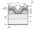
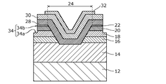
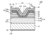
- the nitride semiconductor device 10 includes a substrate 12, a drift layer 14, a first base layer 16, a second base layer 18, a third base layer 20, and a fourth base layer 20. It includes a base layer 22, a gate opening 24, an electron traveling layer 28, an electron supply layer 30, a gate electrode 32, a source opening 34, a source electrode 36, and a drain electrode 38. Further, as shown in FIG. 1A, the nitride semiconductor device 10 includes a gate electrode pad 40 and a source electrode pad 42. In FIG. 1A, the outer shape of the source electrode pad 42 is schematically represented by a broken line.
- the nitride semiconductor device 10 is a device having a laminated structure of semiconductor layers mainly composed of nitride semiconductors such as GaN and AlGaN. Specifically, the nitride semiconductor device 10 has a heterostructure of an AlGaN film and a GaN film.
- the interface has a characteristic that a sheet carrier concentration of 1 ⁇ 10 13 cm- 2 or more can be obtained.
- the nitride semiconductor device 10 has a plurality of heterostructures. Specifically, the laminated structure of the drift layer 14 and the first base layer 16 and the laminated structure of the electron traveling layer 28 and the electron supply layer 30 form a heterostructure, respectively.
- a two-dimensional electron gas 46 is generated in the vicinity of the interface between the drift layer 14 and the first base layer 16.
- a two-dimensional electron gas 44 is generated in the vicinity of the interface between the electron traveling layer 28 and the electron supply layer 30.
- the nitride semiconductor device 10 according to the present embodiment is a field effect transistor (FET) that uses a two-dimensional electron gas 44 generated in the electron traveling layer 28 as a channel.
- the nitride semiconductor device 10 is a so-called vertical FET.
- the two-dimensional electron gases 44 and 46 are schematically shown by broken lines, respectively.
- the substrate 12 is a substrate made of a nitride semiconductor, and has a first main surface 12a and a second main surface 12b facing each other as shown in FIG.
- the first main surface 12a is the main surface on the side where the drift layer 14 is formed.
- the first main surface 12a substantially coincides with the c surface.
- the second main surface 12b is the main surface on the opposite side of the first main surface 12a, and is the main surface on the side on which the drain electrode 38 is formed.
- the plan view shape of the substrate 12 is, for example, rectangular, but is not limited to this.
- the substrate 12 is, for example, a substrate made of n-type GaN having a thickness of 300 ⁇ m and a carrier concentration of 1 ⁇ 10 18 cm -3.
- the n-type and p-type indicate the conductive type of the semiconductor.
- the n-type is an example of the first conductive type of the nitride semiconductor.
- the p-type is an example of a second conductive type having a polarity different from that of the first conductive type.
- the substrate 12 does not have to be a nitride semiconductor substrate.
- the substrate 12 may be a silicon (Si) substrate, a silicon carbide (SiC) substrate, a zinc oxide (ZnO) substrate, or the like.
- the drift layer 14 is an example of a first electron traveling layer having a first conductive type, which is provided above the first main surface 12a of the substrate 12.
- the drift layer 14 is composed of a first conductive type nitride semiconductor.
- the drift layer 14 is, for example, a film made of n-type GaN having a thickness of 8 ⁇ m and a carrier concentration of 1 ⁇ 10 16 cm -3.
- the drift layer 14 is provided in contact with the first main surface 12a of the substrate 12.
- the first base layer 16 is an example of a first electron supply layer provided above the drift layer 14.
- the first base layer 16 is made of a nitride semiconductor.
- the first base layer 16 is, for example, a film made of undoped Al 0.2 Ga 0.8 N having a thickness of 50 nm.
- the first base layer 16 forms an AlGaN / GaN hetero interface with the drift layer 14. As a result, the two-dimensional electron gas 46 is generated in the drift layer 14.
- the second base layer 18 is an example of a first nitride semiconductor layer provided above the first base layer 16 and having a second conductive type different from the first conductive type.
- the second base layer 18 is, for example, a film made of p-type GaN having a thickness of 400 nm and a carrier concentration of 1 ⁇ 10 17 cm -3.
- the second base layer 18 is provided in contact with the upper surface of the first base layer 16.
- the second base layer 18 suppresses the leakage current between the source electrode 36 and the drain electrode 38.
- the drain electrode 38 has a higher potential than the source electrode 36.
- the depletion layer extends to the drift layer 14. This makes it possible to increase the withstand voltage of the nitride semiconductor device 10.
- the third base layer 20 is arranged on the second base layer 18.
- the third base layer 20 is formed of an insulating or semi-insulating nitride semiconductor.
- the third base layer 20 is, for example, a film made of undoped GaN having a thickness of 200 nm.
- the third base layer 20 is provided in contact with the second base layer 18.
- the third base layer 20 is doped with carbon. Specifically, the carbon concentration of the third base layer 20 is higher than the carbon concentration of the second base layer 18.
- the third base layer 20 may contain silicon (Si) or oxygen (O) mixed during film formation.
- the carbon concentration of the third base layer 20 is, for example, 3 ⁇ 10 17 cm -3 or more, but may be 1 ⁇ 10 18 cm -3 or more.
- the silicon concentration or oxygen concentration of the third base layer 20 is, for example, 5 ⁇ 10 16 cm -3 or less, but may be 2 ⁇ 10 16 cm -3 or less.
- an n-type electron supply layer 30 and an electron traveling layer 28 / p type are located between the source electrode 36 and the drain electrode 38.
- the second base layer 18 / n-type first base layer 16 and the n-type drift layer 14 have a laminated structure.
- This laminated structure is a parasitic bipolar transistor having a parasitic npn structure.
- the parasitic bipolar transistor turns on, which may reduce the withstand voltage of the nitride semiconductor device 10. In this case, the nitride semiconductor device 10 is likely to malfunction.
- the third base layer 20 suppresses the formation of this parasitic npn structure. Therefore, it is possible to reduce the malfunction of the nitride semiconductor device 10 due to the formation of the parasitic npn structure.
- the nitride semiconductor device 10 does not have to include the third base layer 20.
- the fourth base layer 22 is arranged on the third base layer 20.
- the fourth base layer 22 is, for example, a film made of Al 0.2 Ga 0.8 N having a thickness of 20 nm.
- the fourth base layer 22 is provided in contact with the third base layer 20.
- the fourth base layer 22 suppresses the diffusion of p-type impurities such as Mg from the second base layer 18. If Mg diffuses into the channels in the electron traveling layer 28, the carrier concentration of the two-dimensional electron gas 44 may decrease and the on-resistance may increase. The degree of diffusion of Mg also differs depending on the growth conditions of epitaxial growth and the like. Therefore, when the diffusion of Mg is suppressed, the nitride semiconductor device 10 does not have to include the fourth base layer 22.
- the fourth base layer 22 may have a function of supplying electrons to a channel formed at an interface between the electron traveling layer 28 and the electron supply layer 30.
- the fourth base layer 22 has a larger bandgap than, for example, the electron supply layer 30.
- the gate opening 24 is an example of a first opening that penetrates the first base layer 16 and reaches the drift layer 14.
- the gate opening 24 includes a fourth base layer 22, a third base layer 20, a second base layer 18, and a first base layer 16 from the upper surface of the fourth base layer 22. It penetrates in order and reaches the drift layer 14.
- the bottom portion 24a of the gate opening 24 is the upper surface of the drift layer 14. In the present embodiment, as shown in FIG. 2, the bottom portion 24a of the gate opening 24 is located below the interface between the drift layer 14 and the first base layer 16.
- the gate opening 24 is formed so that the opening area becomes larger as the distance from the substrate 12 increases.
- the side wall portion 24b of the gate opening 24 is obliquely inclined.
- the cross-sectional shape of the gate opening 24 is an inverted trapezoid, more specifically, an inverted isosceles trapezoid.
- FIG. 1B the outline of the upper end of the gate opening 24 is shown by a broken line.
- the contour of the bottom 24a of the gate opening 24 is one size smaller than the contour shown in FIG. 1 (b).
- the electronic traveling layer 28 is an example of the second electronic traveling layer provided in the upper portion of the second base layer 18 and the portion along the inner surface of the gate opening 24.
- the electron traveling layer 28 is a first regrowth layer formed by regrowth of a nitride semiconductor after forming the gate opening 24.
- the electron traveling layer 28 is formed with a substantially uniform thickness along the upper surface of the fourth base layer 22 and the side wall portion 24b and the bottom portion 24a of the gate opening 24.
- the electron traveling layer 28 is, for example, a film made of undoped GaN having a thickness of 100 nm.
- the electronic traveling layer 28 is in contact with the drift layer 14 at the bottom 24a of the gate opening 24.
- the electronic traveling layer 28 comes into contact with the side surfaces of the first base layer 16, the second base layer 18, the third base layer 20, and the fourth base layer 22 at the side wall portion 24b of the gate opening 24. ing. Further, the electronic traveling layer 28 is in contact with the upper surface of the fourth base layer 22.
- the electronic traveling layer 28 has a channel. Specifically, a two-dimensional electron gas 44 is generated in the vicinity of the interface between the electron traveling layer 28 and the electron supply layer 30.
- the two-dimensional electron gas 44 functions as a channel of the electron traveling layer 28.
- the electron traveling layer 28 is undoped, it may be n-typed by Si doping or the like.
- an AlN film having a thickness of about 1 nm is provided as a second regrowth layer between the electron traveling layer 28 and the electron supply layer 30.
- the AlN film can suppress alloy scattering and improve the mobility of the channel.
- the AlN film may not be provided, and the electron traveling layer 28 and the electron supply layer 30 may be in direct contact with each other.
- the electron supply layer 30 is an example of a second electron supply layer provided above the second base layer 18 and along the inner surface of the gate opening 24.
- the electron supply layer 30 is a third regrowth layer formed by regrowth of the nitride semiconductor after forming the gate opening 24.
- the electron traveling layer 28 and the electron supply layer 30 are provided in this order from the substrate 12 side.
- the electron supply layer 30 has a shape along the upper surface of the electron traveling layer 28 and is formed with a substantially uniform thickness.
- the electron supply layer 30 is, for example, a film made of undoped Al 0.2 Ga 0.8 N having a thickness of 50 nm.
- the electron supply layer 30 forms, for example, an AlGaN / GaN hetero interface with the electron traveling layer 28 with an AlN film having a thickness of 1 nm interposed therebetween. As a result, the two-dimensional electron gas 44 is generated in the electron traveling layer 28.
- the electron supply layer 30 supplies electrons to a channel (that is, a two-dimensional electron gas 44) formed in the electron traveling layer 28.
- the fourth base layer 22 also has an electron supply function.
- Both the electron supply layer 30 and the fourth base layer 22 are formed of AlGaN, but the Al composition ratio at this time is not particularly limited.
- the Al composition ratio of the electron supply layer 30 may be 20%, and the Al composition ratio of the fourth base layer 22 may be 25%.
- the gate electrode 32 is provided above the electron supply layer 30 and so as to cover the gate opening 24.
- the gate electrode 32 has a shape along the upper surface of the electron supply layer 30 and is formed in contact with the upper surface of the electron supply layer 30 to have a substantially uniform thickness.
- the gate electrode 32 is formed by using a conductive material such as metal.
- the gate electrode 32 is formed using palladium (Pd).
- Pd palladium
- a material that is Schottky-connected to the n-type semiconductor can be used. Can be used.
- the gate electrode 32 is formed so as to be separated from each other in a plan view so as not to come into contact with the source electrode 36. Specifically, as shown in FIG. 1B, the gate electrode 32 is provided so as to surround the source electrode 36 in a plan view. More specifically, the gate electrode 32 is formed in the shape of a single plate provided with a plurality of openings corresponding to the hexagonal source electrode 36.
- the end portion of the gate electrode 32 is located closer to the source electrode 36 than the end portion of the gate opening 24 in a plan view.
- a gate opening 24 is provided inside the gate electrode 32. That is, in a plan view, the gate electrode 32 completely covers the gate opening 24.
- the source opening 34 is an example of a second opening that penetrates the electron traveling layer 28 and reaches the second base layer 18 at a position away from the gate electrode 32. Specifically, the source opening 34 penetrates the electron supply layer 30, the electron traveling layer 28, the fourth base layer 22, and the third base layer 20 in this order, and reaches the second base layer 18. There is. In the present embodiment, as shown in FIG. 2, the bottom portion 34a of the source opening 34 is the upper surface of the second base layer 18. The bottom portion 34a is located below the interface between the second base layer 18 and the third base layer 20. The source opening 34 is arranged at a position away from the gate opening 24 in a plan view.
- the opening area of the source opening 34 is formed to be substantially constant.
- the side wall portion 34b of the source opening 34 is substantially parallel along the thickness direction of the substrate 12.
- the cross-sectional shape of the source opening 34 is rectangular.
- the cross-sectional shape of the source opening 34 may be an inverted trapezoid like the gate opening 24.
- the opening shape of the source opening 34 is a regular hexagon as shown in FIG. 1 (b).
- the distance from the gate electrode 32 provided so as to surround the outer circumference of the source opening 34 is substantially constant.
- the side wall 34b of the source opening 34 has a ⁇ 1-100 ⁇ plane.
- the ⁇ 1-100 ⁇ plane is a general term for the (1-100) plane and the plane equivalent to the (1-100) plane.
- the source electrode 36 is provided in the source opening 34. Specifically, the source electrode 36 is provided so as to fill the inside of the source opening 34.
- the source electrode 36 is connected to the second base layer 18. Specifically, the source electrode 36 is connected to each end face of the electron supply layer 30, the electron traveling layer 28, the fourth base layer 22, and the third base layer 20. The source electrode 36 is ohmicly connected to the electron traveling layer 28 and the electron supply layer 30.
- the source electrode 36 is formed by using a conductive material such as metal.
- a conductive material such as metal.
- a material such as Ti / Al that is ohmic-connected to the n-type semiconductor layer can be used.
- the potential of the third base layer 20 can be fixed. As a result, the operation of the nitride semiconductor device 10 can be stabilized.
- Al is shot key connected to the second base layer 18 made of a p-type nitride semiconductor. Therefore, a metal material having a large work function such as Pd or Ni, which has a low contact resistance with respect to the p-type nitride semiconductor, may be provided in the lower layer portion of the source electrode 36. As a result, the potential of the second base layer 18 can be made more stable.
- the drain electrode 38 is provided on the second main surface 12b side of the substrate 12. Specifically, the drain electrode 38 is provided in contact with the second main surface 12b.
- the drain electrode 38 is formed by using a conductive material such as metal.
- a material that is ohmic-connected to the n-type semiconductor layer, such as Ti / Al, can be used.
- the gate electrode pad 40 is electrically connected to the gate electrode 32.
- the gate electrode pad 40 is provided above, for example, the gate electrode 32.
- the gate electrode pad 40 is a part of the nitride semiconductor device 10 in a plan view. It is provided only in the area of.
- a power supply for controlling the gate electrode 32 is connected to the gate electrode pad 40.
- the source electrode pad 42 is electrically connected to each of the plurality of source electrodes 36.
- the source electrode pad 42 is provided above the source electrode 36.
- each of the plurality of source electrodes 36 is formed in a hexagonal island shape. Therefore, the source electrode pad 42 is provided in most of the regions excluding the gate electrode pad 40 in the plan view of the nitride semiconductor device 10 so as to cover each of the plurality of source electrodes 36.
- the interface between the electron traveling layer 28 and the electron supply layer 30 is an AlGaN / GaN hetero interface.
- the two-dimensional electron gas 44 is generated in the electron traveling layer 28, and a channel is formed. Since the two-dimensional electron gas 44 has a high carrier concentration, the mobility of the channel is high, and the resistance value (on resistance) during operation is reduced.
- the two-dimensional electron gas 46 is parallel to the first main surface 12a of the substrate 12 in the drift layer 14 from the vicinity of the bottom portion 24a of the gate opening 24 in the lateral direction (specifically, parallel to the first main surface 12a of the substrate 12). It is formed so as to extend in the direction). Therefore, the electrons moving through the two-dimensional electron gas 44 in the electron traveling layer 28 tend to spread laterally through the two-dimensional electron gas 46 in the vicinity of the bottom portion 24a. Therefore, in the drift layer 14, not only the portion located directly below the bottom portion 24a but also the portion located outside the portion (outside the bottom portion 24a in a plan view) can be used as a current flow path. Therefore, the source-drain current is likely to be diffused over a wide area in the drift layer 14. Therefore, the resistance value during operation of the nitride semiconductor device 10 can be reduced.
- FIGS. 3A to 3F are cross-sectional views showing each step of the manufacturing method of the nitride semiconductor device 10 according to the present embodiment.
- each nitride semiconductor layer constituting the nitride semiconductor device 10 is formed by a metalorganic vapor phase epitaxy (MOVPE) method.
- MOVPE metalorganic vapor phase epitaxy
- the method for forming the nitride semiconductor layer is not limited to this, and for example, a molecular beam epitaxy (MBE) method may be used for forming the nitride semiconductor layer.
- MBE molecular beam epitaxy
- the n-type nitride semiconductor is formed by adding, for example, silicon (Si).
- the p-type nitride semiconductor is formed by adding magnesium (Mg).
- the n-type impurities and p-type impurities are not limited to these.
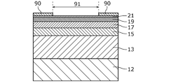
- a substrate 12 made of n-type GaN whose first main surface 12a is a (0001) surface, that is, a c surface is prepared.
- An undoped AlGaN film 21 composed of a p-type GaN film 17 to which Mg is added as a p-type impurity, an undoped GaN film 19, and an undoped Al 0.2 Ga 0.8 N is formed in this order.
- the n-type GaN film 13, the undoped AlGaN film 15, the p-type GaN film 17, the undoped GaN film 19, and the undoped AlGaN film 21 are each patterned into a predetermined shape, whereby the drift layer 14 and the first are shown in FIG. It becomes the base layer 16, the second base layer 18, the third base layer 20, and the fourth base layer 22.
- the thickness and carrier concentration of each layer are as follows, for example.
- the n-type GaN film 13 has a thickness of 8 ⁇ m and a carrier concentration of 1 ⁇ 10 16 cm -3 .
- the undoped AlGaN film 15 has a thickness of 20 nm.
- the p-type GaN film 17 has a thickness of 400 nm and a carrier concentration of 1 ⁇ 10 17 cm -3 .
- the undoped GaN film 19 has a thickness of 200 nm.
- the undoped AlGaN film 21 has a thickness of 20 nm.
- a resist is applied onto the undoped AlGaN film 21, and the applied resist is patterned by photolithography to form a resist mask 90.
- the resist mask 90 is a mask for forming the gate opening 24, and has an opening 91 corresponding to the plan view shape of the gate opening 24.
- the gate opening 24 is formed by dry etching.
- the gate opening 24 penetrates the undoped AlGaN film 21, the undoped GaN film 19, the p-type GaN film 17, and the undoped AlGaN film 15, and the n-type GaN film 13 is exposed.
- the bottom portion 24a of the gate opening 24 is parallel to the first main surface 12a of the substrate 12.
- the side wall portion 24b of the gate opening 24 is inclined at a predetermined inclination angle with respect to the bottom portion 24a.
- the inclination angle is, for example, in the range of 20 ° or more and 80 ° or less.
- the regrowth layer can be formed on the side wall portion 24b with a uniform thickness, so that narrowing of the channel can be suppressed, and both a decrease in the carrier concentration and an increase in the on-resistance can be suppressed.
- the undoped GaN film 27, the undoped AlN film (not shown), and the undoped AlGaN film 29 are applied to the entire surface along the shape of the gate opening 24. Is formed in this order by the MOVPE method.
- the undoped GaN film 27 and the undoped AlGaN film 29 are patterned into a predetermined shape to form an electron traveling layer 28 and an electron supply layer 30, respectively.
- each layer is substantially uniform.
- the undoped GaN film 27, which is as follows has a thickness of 100 nm.
- the undoped AlN film has a thickness of 1 nm.
- the undoped AlGaN film 29 has a thickness of 50 nm.
- a gate metal film made of Pd is formed by a vapor deposition method, a sputtering method, or the like so as to cover the gate opening 24.
- the gate electrode 32 is formed by patterning the formed gate metal film.
- the undoped AlGaN film 29, the undoped AlN film (not shown), the undoped GaN film 27, the undoped AlGaN film 21, and the undoped GaN film 19 penetrate at a position away from the gate electrode 32. Then, the source opening 34 that reaches the p-type GaN film 17 is formed. The formation of the source opening 34 is formed by photolithography and dry etching, similarly to the gate opening 24.
- the electron supply layer 30, the electron traveling layer 28, and the fourth base layer 22 are patterned.
- a third base layer 20 and a second base layer 18 are formed.
- a source metal film composed of Ti and Au is formed into a film by a vapor deposition method, a sputtering method, or the like so as to fill the source opening 34, and the source electrode 36 is formed by patterning.
- a drain metal film composed of Ti and Al is formed on the second main surface 12b of the substrate 12 by a vapor deposition method, a sputtering method, or the like, and patterned as necessary to form the drain electrode 38.
- the nitride semiconductor device 10 shown in FIG. 2 is formed.
- the gate electrode 32 and the source electrode 36 After forming the gate electrode 32 and the source electrode 36, an insulating film was formed, and a contact hole was formed to expose a part of each of the plurality of source electrodes 36 and a part of the gate electrode 32. It is formed on an insulating film. After that, the gate electrode pad 40 and the source electrode pad 42 are formed by forming a metal film and patterning.
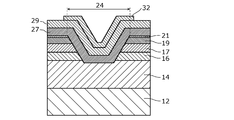
- FIG. 4 is a cross-sectional view of the nitride semiconductor device 110 according to the first modification. As shown in FIG. 4, the nitride semiconductor device 110 is different from the nitride semiconductor device 10 shown in FIG. 2 in that it is newly provided with the high resistance layer 126. In the following, the differences from the embodiments will be mainly described, and the common points will be omitted or simplified.
- the high resistance layer 126 is provided between the second base layer 18 and the electron traveling layer 28 at the gate opening 24.
- the high resistance layer 126 is also provided between the first base layer 16 and the electron traveling layer 28.
- the high resistance layer 126 is provided from the side wall portion 24b of the gate opening 24 to a part of the bottom portion 24a. More specifically, the high resistance layer 126 covers the entire surface of the side wall portion 24b from the upper end portion of the gate opening 24, that is, a part of the upper surface of the fourth base layer 22, to a part of the bottom portion 24a. It is provided to cover it. That is, the high resistance layer 126 is provided between each of the first base layer 16, the second base layer 18, the third base layer 20, and the fourth base layer 22 and the electron traveling layer 28. ..
- the upper surface of the upper end portion of the high resistance layer 126 is flush with the upper surface of the fourth base layer 22. Further, the upper surface of the lower end portion of the high resistance layer 126 is flush with the portion of the upper surface of the drift layer 14 that forms the bottom portion 24a.
- the high resistance layer 126 includes a surface layer portion and an end face portion of the fourth base layer 22, an end face portion of the third base layer 20, an end face portion of the second base layer 18, an end face portion of the first base layer 16, and the like. , It is formed so as to be embedded in each of the surface layer portions of the drift layer 14.
- the high resistance layer 126 has a higher resistance value than the second base layer 18. In this modification, the high resistance layer 126 has a higher resistance value than the third base layer 20.
- the high resistance layer 126 is made of a nitride semiconductor. In this modification, the high resistance layer 126 contains iron (Fe).
- the high resistance layer 126 is made of, for example, iron-doped and high resistance GaN.
- the thickness of the high resistance layer 126 is, for example, 50 nm.
- FIGS. 5A and 5B are cross-sectional views showing a method of manufacturing the nitride semiconductor device 110 according to the present modification.
- the manufacturing method of the nitride semiconductor device 110 according to the present modification is the same as that of the nitride semiconductor device 10 according to the first embodiment in the process until the gate opening 24 is formed.
- the resist mask 90 is removed.
- the resist is applied again on the undoped AlGaN film 21 and in the gate opening 24.
- the resist mask 192 is formed by patterning the applied resist by photolithography.
- the resist mask 192 is a mask for forming the high resistance layer 126.
- the resist mask 192 has an opening 193 that is larger than the side wall portion 24b of the gate opening 24.
- the opening 193 is provided from the upper end of the side wall portion 24b to a part of the upper surface portion of the undoped AlGaN film 21 to a part of the bottom portion 24a, and exposes at least the entire side wall portion 24b in a plan view.
- the high resistance layer 126 is formed by implanting iron ions into the portion of the resist mask 192 exposed to the opening 193.
- the high resistance layer 126 is a layer in which iron is doped in the portion exposed in the opening 193 of each of the undoped AlGaN film 21, the undoped GaN film 19, the p-type GaN film 17, the undoped AlGaN film 15 and the n-type GaN film 13. is there.
- the portion of the n-type GaN film 13 excluding the high resistance layer 126 becomes the drift layer 14.
- the injection conditions for ion implantation are, for example, an acceleration energy of 40 keV and a dose amount of 1 ⁇ 10 14 cm- 2 .
- the high resistance layer 126 having a thickness of about 50 nm is formed.
- the region into which iron ions are injected, that is, the high resistance layer 126 is increased in resistance by breaking the crystal structure and becoming an amorphous state.
- a metal ion having a large atomic number such as titanium ion, chromium ion, copper ion or nickel ion may be used.
- the process after forming the high resistance layer 126 is the same as that of the nitride semiconductor device 10 according to the first embodiment. Specifically, after the high resistance layer 126 is formed, as shown in FIG. 3D, the undoped GaN film 27, the undoped AlN film (not shown), and the undoped AlGaN film 29 are sequentially formed by regrowth. Since the high resistance layer 126 is made of a nitride semiconductor, the film quality is improved by the regrowth of the undoped GaN film 27, the undoped AlN film (not shown) and the undoped AlGaN film 29.
- the source electrode 36 is used to connect the second base layer 18 and the electron traveling. Leakage current through the layer 28 to the gate electrode 32 can be suppressed. As described above, according to this modification, the nitride semiconductor device 110 in which the leakage current is suppressed is realized.
- the resist mask 192 may be formed so that the opening 193 exposes only the p-type GaN film 17 at the side wall portion 24b. That is, the plan-view shape of the opening 193 may coincide with the boundary between the p-type GaN film 17 and the undoped GaN film 19 and the boundary between the p-type GaN film 17 and the undoped AlGaN film 15.
- the resist mask 192 may be formed so that the opening 193 exposes the entire p-type GaN film 17 and the entire undoped AlGaN film 15 at the side wall portion 24b.
- FIG. 6 is a cross-sectional view of the nitride semiconductor device 210 according to the second modification. As shown in FIG. 6, the nitride semiconductor device 210 is different from the nitride semiconductor device 10 shown in FIG. 2 in that it includes a threshold control layer 248. In the following, the differences from the first embodiment will be mainly described, and the common points will be omitted or simplified.
- the threshold control layer 248 is an example of a second conductive type second nitride semiconductor layer provided between the gate electrode 32 and the electron traveling layer 28.
- the threshold control layer 248 is provided on the electron supply layer 30, and is in contact with the electron supply layer 30 and the gate electrode 32.
- the end portion of the threshold control layer 248 is located closer to the source electrode 36 than the end portion of the gate electrode 32.
- the threshold control layer 248 and the source electrode 36 are separated from each other and are not in contact with each other.
- the threshold control layer 248 is, for example, a nitride semiconductor layer made of p-type Al 0.2 Ga 0.8 N having a thickness of 100 nm and a carrier concentration of 1 ⁇ 10 17 cm -3.
- the threshold control layer 248 is formed by forming a film of the undoped AlGaN film 29 forming the electron supply layer 30 and then forming a film by the MOVPE method and patterning the film.
- the threshold control layer 248 raises the potential of the conduction band end of the channel portion. Therefore, the threshold voltage of the nitride semiconductor device 210 can be increased. Therefore, the nitride semiconductor device 210 can be realized as a normally-off type FET.
- the threshold control layer 248 may be formed by using an insulating material. That is, the threshold control layer 248 may be an insulating layer.
- the second embodiment is different from the first embodiment in that the first electron traveling layer has a two-layer structure.
- the differences from the first embodiment will be mainly described, and the common points will be omitted or simplified.
- FIG. 7 is a cross-sectional view of the nitride semiconductor device 310 according to the present embodiment. As shown in FIG. 7, the nitride semiconductor device 310 is different from the nitride semiconductor device 10 shown in FIG. 2 in that it includes an electron traveling layer 314 instead of the drift layer 14.
- the electronic traveling layer 314 is an example of the first electronic traveling layer.
- the electron traveling layer 314 includes a drift layer 314a and an undoped nitride semiconductor layer 314b.
- the drift layer 314a is an example of the first conductive type third nitride semiconductor layer, and is substantially the same as the drift layer 14 according to the first embodiment. In the present embodiment, the only difference is that the gate opening 24 does not reach the drift layer 314a. Therefore, the upper surface of the drift layer 314a is flat.
- the undoped nitride semiconductor layer 314b is an example of an undoped fourth nitride semiconductor layer located between the drift layer 314a and the first base layer 16.
- the undoped nitride semiconductor layer 314b is a film made of undoped GaN.
- the film thickness of the undoped nitride semiconductor layer 314b is, for example, 200 nm, but is not limited thereto.
- the undoped nitride semiconductor layer 314b is in contact with the first base layer 16 and forms an AlGaN / GaN hetero interface with the first base layer 16. As a result, the two-dimensional electron gas 46 is generated in the undoped nitride semiconductor layer 314b.
- the drift layer 314a and the undoped nitride semiconductor layer 314b are formed by, for example, the following method. Specifically, in the manufacturing process shown in FIG. 3A, the undoped GaN film is formed after the n-type GaN film 13 is formed and before the undoped AlGaN film 15 is formed. Then, in the manufacturing process shown in FIG. 3C, the gate opening 24 is formed so as to expose the undoped GaN film. Therefore, in the present embodiment, the bottom portion 24a of the gate opening 24 is the upper surface of the undoped nitride semiconductor layer 314b.
- the source-drain current is likely to be diffused over a wide area in the drift layer 314a.
- the undoped nitride semiconductor layer 314b has few impurities, the electron mobility can be increased. Therefore, the operation speed of the nitride semiconductor device 310 can be increased.
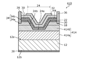
- the third embodiment is different from the first embodiment in that the first electron traveling layer has a two-layer structure and does not include the first electron supply layer.
- the differences from the first embodiment will be mainly described, and the common points will be omitted or simplified.
- FIG. 8 is a cross-sectional view of the nitride semiconductor device 410 according to the present embodiment. As shown in FIG. 8, the nitride semiconductor device 410 is different from the nitride semiconductor device 10 shown in FIG. 2 in that it includes an electron traveling layer 414 instead of the drift layer 14. Further, the nitride semiconductor device 410 does not include the first base layer 16.
- the electronic traveling layer 414 is an example of the first electronic traveling layer.
- the electron traveling layer 414 includes a low-concentration layer 414a and a high-concentration layer 414b.
- the low-concentration layer 414a is an example of the first conductive type third nitride semiconductor layer, and is substantially the same as the drift layer 14 according to the first embodiment. In the present embodiment, the only difference is that the gate opening 24 does not reach the low-concentration layer 414a. Therefore, the upper surface of the low-concentration layer 414a is flat.
- the high-concentration layer 414b is an example of a fourth nitride semiconductor layer located between the low-concentration layer 414a and the second base layer 18 and having a higher impurity concentration than the low-concentration layer 414a.
- the high-concentration layer 414b is a film made of n-type GaN having a higher concentration of n-type impurities than the low-concentration layer 414a.
- the carrier concentration of the high-concentration layer 414b is, for example, 1 ⁇ 10 18 cm -3 or more, but is not limited to this.
- the film thickness of the high-concentration layer 414b is smaller than the film thickness of the low-concentration layer 414a, for example, less than 1 ⁇ m, but is not limited thereto.
- the high concentration layer 414b is in contact with the second base layer 18.
- the difference in bandgap is small in all of the low-concentration layer 414a, the high-concentration layer 414b, and the second base layer 18, and a hetero interface is not formed. Therefore, the two-dimensional electron gas 46 shown in FIG. 2 and the like is not generated.
- Two-dimensional electron gas 46 is not generated, but the high concentration layer 414b has a high concentration of n-type impurities, so its resistance is small. Therefore, the electrons spread laterally in the high concentration layer 414b. Therefore, as in the first embodiment, the source-drain current is likely to be diffused over a wide area in the high-concentration layer 414b and the low-concentration layer 414a.
- the low-concentration layer 414a and the high-concentration layer 414b are formed by, for example, the following method. Specifically, in the manufacturing process shown in FIG. 3A, after the n-type GaN film 13 is formed and before the undoped AlGaN film 15 is formed, the n-type GaN film having a higher impurity concentration than the n-type GaN film 13 is formed. Is formed. Then, in the manufacturing process shown in FIG. 3C, the gate opening 24 is formed so as to expose the n-type GaN film having a high impurity concentration. Therefore, in the present embodiment, the bottom portion 24a of the gate opening 24 is the upper surface of the high-concentration layer 414b.
- the resistance of the high-concentration layer 414b is small, electrons tend to spread in the lateral direction. Therefore, as in the first embodiment, the source-drain current is likely to be diffused over a wide area in the electron traveling layer 414. Therefore, the resistance value during operation can be further reduced.
- the present invention is not limited to this.
- the first conductive type may be p-type
- the second conductive type may be n-type.
- the high resistance layer 126 may be provided only between the electron traveling layer 28 and the second base layer 18.
- the high resistance layer 126 may be provided only on a part of the side wall portion 24b of the gate opening 24, and the end faces of the first base layer 16, the third base layer 20, and the fourth base layer 22. It does not have to cover.
- the end portion of the gate electrode 32 may coincide with the end portion of the gate opening 24.
- the gate electrode 32 may be provided inside the gate opening 24.
- the source opening 34 reaching up to the second base layer 18 is provided, but the present invention is not limited to this.
- the source opening 34 may be an opening that reaches the electron traveling layer 28, and the source electrode 36 may be connected to the electron traveling layer 28 and not to the second base layer 18. Good.
- the drift layer 14 which is an example of the first electron traveling layer may have the same composition as the electron traveling layer 28 which is an example of the second electron traveling layer.
- the carbon concentration of the drift layer 14 may be higher than the carbon concentration of the electron traveling layer 28.
- the carbon concentration of the drift layer 14 may be on the order of 10 18 cm -3
- the carbon concentration of the electron traveling layer 28 may be on the order of 10 16 cm -3.
- the carbon concentration in the drift layer 14 does not have to be uniform.
- the carbon concentration may be low in the surface layer portion of the drift layer 14, that is, in the vicinity of the interface with the first base layer 16.
- the generation of the two-dimensional electron gas 46 can be promoted and the channel mobility can be increased, so that the current can be easily diffused.
- the planar layout of the nitride semiconductor device is not limited to the example shown in FIG.
- the source electrode 36 may have a rectangular shape extending in one direction in a plan view.
- a plurality of source electrodes 36 may be arranged in the lateral direction.
- the lateral direction corresponds to the direction along the II-II line.
- the present disclosure can be used as a nitride semiconductor device having a small resistance value, and can be used, for example, as a power transistor used in a power supply circuit of a consumer device such as a television.
Landscapes
- Junction Field-Effect Transistors (AREA)
Priority Applications (3)
| Application Number | Priority Date | Filing Date | Title |
|---|---|---|---|
| US17/789,682 US12317563B2 (en) | 2020-01-08 | 2020-12-21 | Nitride semiconductor device |
| JP2021569816A JP7605769B2 (ja) | 2020-01-08 | 2020-12-21 | 窒化物半導体装置 |
| JP2024218105A JP2025028178A (ja) | 2020-01-08 | 2024-12-12 | 窒化物半導体装置 |
Applications Claiming Priority (2)
| Application Number | Priority Date | Filing Date | Title |
|---|---|---|---|
| JP2020-001752 | 2020-01-08 | ||
| JP2020001752 | 2020-01-08 |
Publications (1)
| Publication Number | Publication Date |
|---|---|
| WO2021140898A1 true WO2021140898A1 (ja) | 2021-07-15 |
Family
ID=76788585
Family Applications (1)
| Application Number | Title | Priority Date | Filing Date |
|---|---|---|---|
| PCT/JP2020/047685 Ceased WO2021140898A1 (ja) | 2020-01-08 | 2020-12-21 | 窒化物半導体装置 |
Country Status (3)
| Country | Link |
|---|---|
| US (1) | US12317563B2 (https=) |
| JP (2) | JP7605769B2 (https=) |
| WO (1) | WO2021140898A1 (https=) |
Cited By (1)
| Publication number | Priority date | Publication date | Assignee | Title |
|---|---|---|---|---|
| WO2023127187A1 (ja) * | 2021-12-27 | 2023-07-06 | パナソニックホールディングス株式会社 | 窒化物半導体デバイス |
Families Citing this family (1)
| Publication number | Priority date | Publication date | Assignee | Title |
|---|---|---|---|---|
| CN116632045A (zh) * | 2023-06-14 | 2023-08-22 | 杭州士兰集昕微电子有限公司 | 一种氮化镓功率器件及其制造方法 |
Citations (5)
| Publication number | Priority date | Publication date | Assignee | Title |
|---|---|---|---|---|
| JP2004260140A (ja) * | 2003-02-06 | 2004-09-16 | Toyota Central Res & Dev Lab Inc | Iii族窒化物半導体を有する半導体素子 |
| WO2012060206A1 (ja) * | 2010-11-04 | 2012-05-10 | 住友電気工業株式会社 | 半導体装置およびその製造方法 |
| WO2013008422A1 (ja) * | 2011-07-12 | 2013-01-17 | パナソニック株式会社 | 窒化物半導体装置およびその製造方法 |
| WO2019097813A1 (ja) * | 2017-11-16 | 2019-05-23 | パナソニック株式会社 | 窒化物半導体装置 |
| WO2019181391A1 (ja) * | 2018-03-22 | 2019-09-26 | パナソニック株式会社 | 窒化物半導体装置 |
Family Cites Families (8)
| Publication number | Priority date | Publication date | Assignee | Title |
|---|---|---|---|---|
| JP5303948B2 (ja) * | 2008-02-06 | 2013-10-02 | 豊田合成株式会社 | オーミック電極形成方法、および電界効果トランジスタの製造方法 |
| JP5566618B2 (ja) * | 2008-03-07 | 2014-08-06 | 古河電気工業株式会社 | GaN系半導体素子 |
| JP4737471B2 (ja) | 2009-10-08 | 2011-08-03 | 住友電気工業株式会社 | 半導体装置およびその製造方法 |
| JP5353735B2 (ja) | 2010-01-28 | 2013-11-27 | 住友電気工業株式会社 | 半導体装置およびその製造方法 |
| WO2015004853A1 (ja) * | 2013-07-12 | 2015-01-15 | パナソニックIpマネジメント株式会社 | 半導体装置 |
| US9728630B2 (en) * | 2014-09-05 | 2017-08-08 | Infineon Technologies Austria Ag | High-electron-mobility transistor having a buried field plate |
| JP6755892B2 (ja) * | 2016-02-08 | 2020-09-16 | パナソニック株式会社 | 半導体装置 |
| WO2020137303A1 (ja) | 2018-12-27 | 2020-07-02 | パナソニック株式会社 | 窒化物半導体装置 |
-
2020
- 2020-12-21 JP JP2021569816A patent/JP7605769B2/ja active Active
- 2020-12-21 WO PCT/JP2020/047685 patent/WO2021140898A1/ja not_active Ceased
- 2020-12-21 US US17/789,682 patent/US12317563B2/en active Active
-
2024
- 2024-12-12 JP JP2024218105A patent/JP2025028178A/ja active Pending
Patent Citations (5)
| Publication number | Priority date | Publication date | Assignee | Title |
|---|---|---|---|---|
| JP2004260140A (ja) * | 2003-02-06 | 2004-09-16 | Toyota Central Res & Dev Lab Inc | Iii族窒化物半導体を有する半導体素子 |
| WO2012060206A1 (ja) * | 2010-11-04 | 2012-05-10 | 住友電気工業株式会社 | 半導体装置およびその製造方法 |
| WO2013008422A1 (ja) * | 2011-07-12 | 2013-01-17 | パナソニック株式会社 | 窒化物半導体装置およびその製造方法 |
| WO2019097813A1 (ja) * | 2017-11-16 | 2019-05-23 | パナソニック株式会社 | 窒化物半導体装置 |
| WO2019181391A1 (ja) * | 2018-03-22 | 2019-09-26 | パナソニック株式会社 | 窒化物半導体装置 |
Cited By (1)
| Publication number | Priority date | Publication date | Assignee | Title |
|---|---|---|---|---|
| WO2023127187A1 (ja) * | 2021-12-27 | 2023-07-06 | パナソニックホールディングス株式会社 | 窒化物半導体デバイス |
Also Published As
| Publication number | Publication date |
|---|---|
| JPWO2021140898A1 (https=) | 2021-07-15 |
| JP2025028178A (ja) | 2025-02-28 |
| JP7605769B2 (ja) | 2024-12-24 |
| US12317563B2 (en) | 2025-05-27 |
| US20230047842A1 (en) | 2023-02-16 |
Similar Documents
| Publication | Publication Date | Title |
|---|---|---|
| US9837518B2 (en) | Semiconductor device | |
| JP7157138B2 (ja) | 窒化物半導体装置 | |
| JP7195306B2 (ja) | 窒化物半導体装置 | |
| US12087762B2 (en) | Nitride semiconductor device | |
| US8350297B2 (en) | Compound semiconductor device and production method thereof | |
| US12142644B2 (en) | Nitride semiconductor device | |
| JP2006086354A (ja) | 窒化物系半導体装置 | |
| JP7813766B2 (ja) | 窒化物半導体デバイス | |
| US20220254902A1 (en) | Nitride semiconductor device and method of fabricating the same | |
| JP2025028178A (ja) | 窒化物半導体装置 | |
| JPWO2020137303A1 (ja) | 窒化物半導体装置 | |
| WO2021079686A1 (ja) | 窒化物半導体装置 | |
| WO2023042617A1 (ja) | 半導体装置 | |
| WO2023112374A1 (ja) | 窒化物半導体デバイス | |
| US12527023B2 (en) | Nitride semiconductor device | |
| WO2024202190A1 (ja) | 窒化物半導体装置およびその製造方法 | |
| WO2026053501A1 (ja) | 窒化物半導体デバイス | |
| JP2023133798A (ja) | 窒化物半導体デバイス | |
| WO2023127187A1 (ja) | 窒化物半導体デバイス |
Legal Events
| Date | Code | Title | Description |
|---|---|---|---|
| 121 | Ep: the epo has been informed by wipo that ep was designated in this application |
Ref document number: 20911936 Country of ref document: EP Kind code of ref document: A1 |
|
| ENP | Entry into the national phase |
Ref document number: 2021569816 Country of ref document: JP Kind code of ref document: A |
|
| NENP | Non-entry into the national phase |
Ref country code: DE |
|
| 122 | Ep: pct application non-entry in european phase |
Ref document number: 20911936 Country of ref document: EP Kind code of ref document: A1 |
|
| WWG | Wipo information: grant in national office |
Ref document number: 17789682 Country of ref document: US |