WO2021117492A1 - スイッチ装置、電流判定方法及びコンピュータプログラム - Google Patents
スイッチ装置、電流判定方法及びコンピュータプログラム Download PDFInfo
- Publication number
- WO2021117492A1 WO2021117492A1 PCT/JP2020/043937 JP2020043937W WO2021117492A1 WO 2021117492 A1 WO2021117492 A1 WO 2021117492A1 JP 2020043937 W JP2020043937 W JP 2020043937W WO 2021117492 A1 WO2021117492 A1 WO 2021117492A1
- Authority
- WO
- WIPO (PCT)
- Prior art keywords
- switch
- current
- sub
- main switch
- load
- Prior art date
- Legal status (The legal status is an assumption and is not a legal conclusion. Google has not performed a legal analysis and makes no representation as to the accuracy of the status listed.)
- Ceased
Links
Images


Classifications
-
- H—ELECTRICITY
- H02—GENERATION; CONVERSION OR DISTRIBUTION OF ELECTRIC POWER
- H02J—ELECTRIC POWER NETWORKS; CIRCUIT ARRANGEMENTS OR SYSTEMS FOR SUPPLYING OR DISTRIBUTING ELECTRIC POWER; SYSTEMS FOR STORING ELECTRIC ENERGY
- H02J7/00—Circuit arrangements for charging or discharging batteries or for supplying loads from batteries
- H02J7/855—Circuit arrangements for charging or discharging batteries or for supplying loads from batteries with circuits adapted for supplying loads from the battery
-
- H—ELECTRICITY
- H02—GENERATION; CONVERSION OR DISTRIBUTION OF ELECTRIC POWER
- H02J—ELECTRIC POWER NETWORKS; CIRCUIT ARRANGEMENTS OR SYSTEMS FOR SUPPLYING OR DISTRIBUTING ELECTRIC POWER; SYSTEMS FOR STORING ELECTRIC ENERGY
- H02J7/00—Circuit arrangements for charging or discharging batteries or for supplying loads from batteries
- H02J7/50—Circuit arrangements for charging or discharging batteries or for supplying loads from batteries acting upon multiple batteries simultaneously or sequentially
- H02J7/575—Parallel/serial switching of connection of batteries to charge or load circuit
-
- H—ELECTRICITY
- H02—GENERATION; CONVERSION OR DISTRIBUTION OF ELECTRIC POWER
- H02J—ELECTRIC POWER NETWORKS; CIRCUIT ARRANGEMENTS OR SYSTEMS FOR SUPPLYING OR DISTRIBUTING ELECTRIC POWER; SYSTEMS FOR STORING ELECTRIC ENERGY
- H02J1/00—Circuit arrangements for DC mains or DC distribution networks
- H02J1/06—Two-wire DC power distribution systems
-
- H—ELECTRICITY
- H02—GENERATION; CONVERSION OR DISTRIBUTION OF ELECTRIC POWER
- H02J—ELECTRIC POWER NETWORKS; CIRCUIT ARRANGEMENTS OR SYSTEMS FOR SUPPLYING OR DISTRIBUTING ELECTRIC POWER; SYSTEMS FOR STORING ELECTRIC ENERGY
- H02J7/00—Circuit arrangements for charging or discharging batteries or for supplying loads from batteries
- H02J7/14—Circuit arrangements for charging or discharging batteries or for supplying loads from batteries for charging batteries from dynamo-electric generators driven at varying speed, e.g. on vehicle
- H02J7/16—Regulation of the charging current or voltage by variation of field
- H02J7/18—Regulation of the charging current or voltage by variation of field due to variation of ohmic resistance in field circuit, using resistance switching in or out of circuit step by step
-
- H—ELECTRICITY
- H02—GENERATION; CONVERSION OR DISTRIBUTION OF ELECTRIC POWER
- H02J—ELECTRIC POWER NETWORKS; CIRCUIT ARRANGEMENTS OR SYSTEMS FOR SUPPLYING OR DISTRIBUTING ELECTRIC POWER; SYSTEMS FOR STORING ELECTRIC ENERGY
- H02J2105/00—Networks for supplying or distributing electric power characterised by their spatial reach or by the load
- H02J2105/30—Networks for supplying or distributing electric power characterised by their spatial reach or by the load the load networks being external to vehicles, i.e. exchanging power with vehicles
- H02J2105/33—Networks for supplying or distributing electric power characterised by their spatial reach or by the load the load networks being external to vehicles, i.e. exchanging power with vehicles exchanging power with road vehicles
Definitions
- the present disclosure relates to switch devices, current determination methods and computer programs.
- This application claims priority based on Japanese Application No. 2019-225848 filed on December 13, 2019, and incorporates all the contents described in the Japanese application.
- Patent Document 1 discloses a switch device for a vehicle in which a switch is arranged in a current path from a DC power supply to a load.
- the power supply from the DC power supply to the load is controlled by switching the switch on or off.
- the switch device includes a connector detachably connected to a load, a main switch provided in a first current path from a DC power supply to the connector, and a first switch from the DC power supply to the connector.
- a switch circuit provided in a two-current path and having a sub-switch and a processing unit that executes processing are provided, and the resistance value of the switch circuit when the sub-switch is on is higher than the on-resistance value of the main switch.
- the processing unit acquires node voltage information indicating the node voltage of the connection node on the downstream side of the main switch and the sub switch in a state where the main switch is off and the sub switch is on. Then, based on the acquired node voltage information, when the main switch is switched on, a process of determining whether or not the switch current flowing through the main switch is less than the current threshold is executed.
- the main switch provided in the first current path from the DC power supply to the connector detachably connected to the load is off, and the DC power supply is connected to the connector.
- the step of acquiring the node voltage information indicating the node voltage of the connection node on the downstream side of the main switch and the subswitch, and the acquisition Based on the node voltage information, the computer executes a step of determining whether or not the switch current flowing through the main switch is less than the current threshold when the main switch is switched on, and the sub The resistance value of the switch circuit when the switch is on is larger than the on-resistance value of the main switch.
- the main switch provided in the first current path from the DC power supply to the connector detachably connected to the load is off, and the DC power supply is connected to the connector.
- the step of acquiring node voltage information indicating the node voltage of the connection node on the downstream side of the main switch and the subswitch, and the acquired node It is used to cause the computer to perform a step of determining whether or not the switch current flowing through the main switch is less than the current threshold when the main switch is turned on based on the voltage information.
- the resistance value of the switch circuit when the sub-switch is on is larger than the on-resistance value of the main switch.
- the present disclosure can be realized not only as a switch device provided with such a characteristic processing unit, but also as a current determination method in which the characteristic processing is a step, or the step is executed on a computer. It can be realized as a computer program to make it. Further, the present disclosure can be realized as a semiconductor integrated circuit that realizes a part or all of the switch device, or can be realized as a power supply system including the switch device.
- the switch device includes a connector detachably connected to a load, a main switch provided in a first current path from a DC power supply to the connector, and the connector from the DC power supply.
- a switch circuit provided in the second current path to the current and having a sub switch, and a processing unit that executes processing are provided, and the resistance value of the switch circuit when the sub switch is on is the on of the main switch.
- Information is acquired, and based on the acquired node voltage information, a process of determining whether or not the switch current flowing through the main switch is less than the current threshold when the main switch is switched on is executed. ..
- the processing unit calculates the resistance component value of the load based on the acquired node voltage information, and the main switch performs based on the calculated resistance component value.
- a process of determining whether or not the switch current flowing when the switch is turned on is less than the current threshold is executed.
- the switch device is provided in a third current path from the DC power supply to the connector, and one end is connected to a resistor connected to the connection node and one end is connected to the connection node.
- the processing unit acquires the node voltage information when the main switch and the sub switch are off, and the node voltage information acquired when the main switch and the sub switch are off. A process of determining whether or not the load is connected to the connector is executed based on the above.
- the processing unit determines that the load is connected to the connector, the main switch is off and the sub switch is on. Executes the process of acquiring the node voltage information.
- the resistance value of the resistor is larger than the resistance value of the switch circuit when the sub switch is on.
- the processing unit acquires current information indicating the switch current, and the load is applied based on the acquired current information. Executes the process of determining whether or not it is connected to the connector.
- the switch circuit has a second resistor connected in series with the subswitch.
- the main switch when the processing unit suspends operation and the processing unit resumes operation, the main switch is off and the sub switch is on.
- the process of acquiring the node voltage information is executed in a certain state.
- the current flowing when a load having a resistance component value of zero ohm is connected to the connector and the main switch and the sub switch are off and on, respectively, is determined. It is a normal value that does not cause smoke.
- the main switch provided in the first current path from the DC power supply to the connector detachably connected to the load is off, and the DC power supply is Step to acquire node voltage information indicating the node voltage of the connection node on the downstream side of the main switch and the sub switch in a state where the sub switch included in the switch circuit provided in the second current path from the main switch to the connector is on.
- the computer executes a step of determining whether or not the switch current flowing through the main switch is less than the current threshold when the main switch is switched on.
- the resistance value of the switch circuit when the sub switch is on is larger than the on resistance value of the main switch.
- the main switch provided in the first current path from the DC power supply to the connector detachably connected to the load is turned off, and the DC power supply is used.
- the resistance value of the switch circuit when the sub switch is on is larger than the on resistance value of the main switch.
- the sub switch is turned on and the node voltage information is acquired before the main switch is turned on.
- the node voltage is the voltage obtained by the switch circuit and the load dividing the voltage of the DC power supply. Yes, the larger the resistance component value of the load, the larger it is.
- the switch current that flows when the main switch is turned on decreases as the resistance component value of the load increases. Therefore, the higher the node voltage, the smaller the switch current that flows when the main switch is turned on.
- the node voltage information that is, the node voltage
- it is determined whether or not the switch current flowing when the main switch is switched on is less than the current threshold value. If it is determined that the switch current is less than the current threshold, the main switch is switched on. Therefore, the passage of an overcurrent exceeding the current threshold value is prevented.
- the resistance component value of the load is calculated based on the node voltage when the main switch is off and the sub switch is on. Based on the calculated resistance component value, it is determined whether or not the switch current flowing when the main switch is switched on is less than the current threshold value.
- the capacitor when the load is not connected to the connector and the main switch and the sub switch are off, the capacitor is connected until the voltage between both ends of the capacitor becomes the voltage of the DC power supply. Is charged. Therefore, the voltage across the capacitor is high.
- the capacitor when the load is connected to the connector and the main switch and sub switch are off, the capacitor is obtained by dividing the voltage between both ends of the capacitor by the resistor and the load dividing the voltage of the DC power supply. Discharge until the voltage is reached. Therefore, the voltage across the capacitor is low. Therefore, it is possible to determine whether or not the load is connected to the connector based on the node voltage when the main switch and the sub switch are off, that is, the voltage between both ends of the capacitor.
- the switch device when it is determined that the load is connected to the connector, the node voltage information is acquired in a state where the main switch is off and the sub switch is on. .. After that, it is determined whether or not the switch current flowing when the main switch is switched on is less than the current threshold value.
- the resistance value of the resistor is large, so that when one of the main switch and the sub switch is on, the current flowing through the resistor is substantially zero A.
- the switch current flows when the load is connected to the connector.
- the main switch is on and the load is not connected to the connector, no switch current flows. Therefore, when the main switch is on, it can be determined whether or not the load is connected to the connector based on the switch current.
- the resistance value of the switch circuit is large when the sub switch is on. Since the second resistor is connected in series with the sub switch, it is possible to realize a switch circuit having a large resistance value when the sub switch is on even when the on resistance value of the sub switch is small. ..
- the processing unit when the processing unit restarts the operation, the processing unit is the main switch based on the node voltage information acquired in the state where the main switch is off and the sub switch is on. Determines whether the switch current that flows when is switched on is less than the current threshold. Therefore, when the load connected to the connector is changed to a load having a small resistance component value while the processing unit is inactive, the main switch 20 is not accidentally switched on.
- the resistance value of the switch circuit is large when the sub switch is on. Therefore, when a load having a resistance component value of zero ohm is connected to the connector and the main switch and the sub switch are off and on, respectively, the current flowing is small and no smoke is generated.
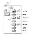
- FIG. 1 is a block diagram showing a main configuration of the power supply system 1 according to the first embodiment.
- the power supply system 1 is preferably mounted on a vehicle and includes a switch device 10, a DC power supply 11, and a load 12.
- the switch device 10 has a main switch 20 and a device connector Ta.
- the load 12 has a load connector Tb.
- the switch device 10 is connected to the positive electrode of the DC power supply 11.
- the negative electrode of the DC power supply 11 is grounded.
- the device connector Ta is detachably connected to the load connector Tb. By connecting the load connector Tb to the device connector Ta, the load 12 is connected to the device connector Ta.
- the DC power supply 11 is, for example, a battery.
- the load 12 is, for example, an electric device brought into a vehicle and has a resistance component. When the electric power supplied to the load 12 is equal to or more than a certain electric power, the load 12 operates. The constant power is a value exceeding zero W. If the power supplied to the load 12 is less than a certain amount, the load 12 stops operating.
- the DC power supply 11 supplies power to the load 12 via the main switch 20 and the device connector Ta. At this time, the electric power supplied to the load 12 is equal to or higher than a certain electric power, and the load 12 operates. In the same case, when the main switch 20 is switched from on to off, the power supplied to the load 12 by the DC power supply 11 is reduced to less than a certain power, and the load 12 stops operating.
- An operation signal instructing the operation of the load 12 and a stop signal instructing the stop of the operation of the load 12 are input to the switch device 10.
- the switch device 10 switches the main switch 20 on and operates the load 12.
- a stop signal is input, the switch device 10 switches the main switch 20 off and stops the operation of the load 12.
- the switch device 10 When a load 12 through which an overcurrent may flow is connected to the device connector Ta, the switch device 10 does not show a notification signal indicating that power cannot be supplied to the load 12. Output to. When an operation signal is input to the switch device 10 when the load 12 is not connected to the device connector Ta, the switch device 10 outputs a notification signal indicating that the load 12 is not connected to a device (not shown).
- the switch device 10 includes a current output circuit 21, a power supply detection unit 22, a microcomputer (hereinafter referred to as a microcomputer) 23, a drive circuit 24, a current resistor 25, a switch circuit 26, and a changeover switch 27. It has a switch resistor 28, a circuit resistor 29, a capacitor 30, and a voltage detection unit 31.
- the switch circuit 26 has a sub switch 40 and switch resistors 41 and 42.
- the main switch 20 is an N-channel type FET (Field Effect Transistor).
- the changeover switch 27 is an NPN type bipolar transistor.
- the sub switch 40 is a P-channel type FET.
- the drain of the main switch 20 is connected to the positive electrode of the DC power supply 11.
- the source of the main switch 20 is connected to the current output circuit 21.
- the current output circuit 21 is further connected to the device connector Ta.
- the device connector Ta is grounded.
- the drain of the main switch 20 is further connected to the power supply detection unit 22.
- the power supply detection unit 22 is connected to the microcomputer 23.
- the gate of the main switch 20 is connected to the drive circuit 24.
- the drive circuit 24 is further connected to the microcomputer 23.
- the current output circuit 21 is further connected to one end of the current resistor 25. The other end of the current resistor 25 is grounded. The connection node between the current output circuit 21 and the current resistor 25 is connected to the microcomputer 23 and the drive circuit 24.
- the drain of the main switch 20 is further connected to the source of the sub switch 40 of the switch circuit 26.
- the drain of the subswitch 40 is connected to the connection node between the current output circuit 21 and the device connector Ta.
- a switch resistor 41 is connected between the source and the gate of the sub switch 40.
- the gate of the subswitch 40 is further connected to one end of the switch resistor 42.
- the other end of the switch resistor 42 is connected to the collector of the changeover switch 27.
- the emitter of the changeover switch 27 is grounded.
- the base of the changeover switch 27 is connected to one end of the switch resistor 28.
- the other end of the switch resistor 28 is connected to the microcomputer 23.
- the drain of the main switch 20 is further connected to one end of the circuit resistor 29.
- the other end of the circuit resistor 29 is connected to a connection node between the current output circuit 21 and the device connector Ta.
- This connection node is further connected to one end of the capacitor 30 and the voltage detection unit 31.
- the other end of the capacitor 30 is grounded.
- the voltage detection unit 31 is connected to the microcomputer 23.
- the power supply detection unit 22 detects the voltage of the DC power supply 11 with reference to the ground potential. In the following, the voltage of the DC power supply 11 based on the ground potential will be referred to as a power supply voltage.
- the power supply detection unit 22 outputs power supply voltage information indicating the detected power supply voltage to the microcomputer 23.
- the power supply voltage information is an analog value, for example, a voltage proportional to the detected power supply voltage.
- the DC power supply 11 supplies power to one or more second loads (not shown) in addition to the load 12.
- the positive electrode of the DC power supply 11 is connected not only to the switch device 10 but also to one or more second loads.
- the power supply voltage of the DC power supply 11 fluctuates according to the current flowing from the DC power supply 11. The larger the current flowing from the DC power supply 11, the lower the power supply voltage.
- the main switch 20 when the gate voltage based on the source potential is a certain voltage or more, the resistance value between the drain and the source is sufficiently small. At this time, the main switch 20 is on, and current can flow through the drain and the source. In the main switch 20, when the gate voltage with respect to the source potential is less than a constant voltage, the resistance value between the drain and the source is sufficiently large. At this time, the main switch 20 is off, and no current flows through the drain and the source.
- An operation signal and a stop signal are input to the microcomputer 23.
- an ON instruction for switching the main switch 20 to ON is output to the drive circuit 24.
- the drive circuit 24 raises the voltage of the gate of the main switch 20 with reference to the ground potential. As a result, in the main switch 20, the voltage of the gate with respect to the source becomes a constant voltage or more, and the main switch 20 is switched on.
- the microcomputer 23 When the stop signal is input to the microcomputer 23, the microcomputer 23 outputs an off instruction instructing the main switch 20 to be turned off to the drive circuit 24.
- the off instruction When the off instruction is input to the drive circuit 24, the voltage of the gate with reference to the ground potential is lowered in the main switch 20. As a result, in the main switch 20, the gate voltage based on the potential of the source becomes less than a constant voltage, and the main switch 20 is switched off. As described above, the drive circuit 24 switches the main switch 20 on or off.
- the load 12 When the load 12 is connected to the device connector Ta, when the main switch 20 is on, the current flows from the positive electrode of the DC power supply 11 in the order of the main switch 20, the current output circuit 21, the device connector Ta, and the load 12. Flows. As a result, the load 12 operates.
- the current that flows from the DC power supply 11 to the main switch 20 and the current output circuit 21 in this order and is output from one end of the current output circuit 21 on the device connector Ta side is referred to as a switch current.
- the current path of the current flowing in this order from the positive electrode of the DC power supply 11 to the main switch 20, the current output circuit 21, and the device connector Ta corresponds to the first current path.
- a main switch 20 is provided in the first current path.
- the current output circuit 21 When the switch current flows, the current output circuit 21 outputs a current that is a predetermined fraction of the switch current to the current resistor 25.
- the current output circuit 21 includes, for example, a current mirror circuit.
- the predetermined number is, for example, 1000.
- the voltage between both ends of the current resistor 25 is input to the microcomputer 23 and the drive circuit 24 as current information.
- the switch current, the resistance value of the current resistance 25, and the predetermined number are described as Is, rc, and N, respectively.
- the voltage between both ends of the current resistor 25 is calculated by Is ⁇ rc / N. " ⁇ " Represents a product.
- the resistance value rc and the predetermined number N are constant values. Therefore, the voltage between both ends of the current resistor 25 is proportional to the switch current Is, and the current information indicates the switch current Is.
- the switch current does not flow regardless of whether the main switch 20 is on or not. Further, even when the main switch 20 is off, the switch current does not flow.
- the current output circuit 21 does not output the current to the current resistor 25, and zero V is input to the microcomputer 23 and the drive circuit 24 as current information.
- the drive circuit 24 switches the main switch 20 off regardless of the signal input from the microcomputer 23. After switching the main switch 20 off, the drive circuit 24 keeps the main switch 20 off regardless of the input current information.
- the cutoff threshold is a constant value and is preset.
- the changeover switch 27 when the base voltage based on the potential of the emitter is a certain voltage or more, the resistance value between the collector and the emitter is sufficiently small. At this time, the changeover switch 27 is on, and current can flow through the collector and the emitter. For the changeover switch 27, when the base voltage based on the potential of the emitter is less than a constant voltage, the resistance value between the collector and the emitter is sufficiently large. At this time, the changeover switch 27 is off, and no current flows through the collector and the emitter.
- the microcomputer 23 raises the base voltage of the changeover switch 27 with reference to the ground potential. As a result, in the changeover switch 27, the base voltage based on the potential of the emitter becomes a constant voltage or more, and the changeover switch 27 is switched on. The microcomputer 23 lowers the voltage at the base of the changeover switch 27 with reference to the ground potential. As a result, in the changeover switch 27, the base voltage based on the potential of the emitter becomes less than a constant voltage, and the changeover switch 27 is switched off. As described above, the microcomputer 23 switches the changeover switch 27 on or off.
- the sub switch 40 of the switch circuit 26 when the gate voltage based on the source potential is less than a constant voltage, the resistance value between the source and drain is sufficiently small. At this time, the sub switch 40 is on, and current can flow through the source and drain.
- the subswitch 40 of the switch circuit 26 when the gate voltage based on the source potential is a constant voltage or more, the resistance value between the source and the drain is sufficiently large. At this time, the sub switch 40 is off, and no current flows through the source and drain.
- the constant voltage for the subswitch 40 is less than zero V.
- the microcomputer 23 switches the changeover switch 27 off, the current flow through the switch resistors 41 and 42 is stopped. As a result, in the sub switch 40, the voltage of the gate based on the potential of the source rises to zero V and exceeds a constant voltage. As a result, the sub switch 40 is switched off. As described above, the microcomputer 23 switches the sub switch 40 on by switching the changeover switch 27 on, and switches the sub switch 40 off by switching the changeover switch 27 off.
- the on-resistance value of the sub-switch 40 that is, the resistance value of the switch circuit 26 when the sub-switch 40 is on is sufficiently larger than the on-resistance value of the main switch 20.
- the resistance value of the circuit resistance 29 is sufficiently larger than the on-resistance value of the subswitch 40, that is, the resistance value of the switch circuit 26 when the subswitch 40 is on.
- the on-resistance value of the main switch 20 is, for example, several ohms.
- the on-resistance value of the subswitch 40 is, for example, a resistance value belonging to the range of several hundred ohms to several kiloohms.
- the on-resistance value of an N-channel FET is usually several ohms or less. Therefore, as the sub switch 40, a P-channel type FET having a large on-resistance value is used.
- the circuit resistance is, for example, several megaohms.
- the on-resistance value of the switch is the resistance value of the switch when the switch is on.
- the voltage detection unit 31 detects the voltage of the connection node between the current output circuit 21 and the device connector Ta.
- the voltage of the connection node between the current output circuit 21 and the device connector Ta will be referred to as a node voltage.
- the node voltage is a voltage based on the ground potential.
- the voltage detection unit 31 outputs node voltage information indicating the detected node voltage to the microcomputer 23.
- the node voltage information is an analog value and indicates, for example, a voltage proportional to the node voltage.
- the microcomputer 23 determines whether or not the load 12 is connected to the device connector Ta based on the node voltage information acquired from the voltage detection unit 31 with the main switch 20 and the sub switch 40 turned off.
- the microcomputer 23 determines that the load 12 is connected to the device connector Ta, the power supply acquired from the power supply detection unit 22 and the voltage detection unit 31 with the main switch 20 turned off and the sub switch 40 turned on.
- the resistance component value of the load 12 is calculated based on the voltage information and the node voltage information.
- the microcomputer 23 determines whether or not the switch current that flows when the main switch 20 is switched on is less than the current threshold value.
- the current threshold is a constant value and is preset. The current threshold is less than the above-mentioned cutoff threshold.
- the microcomputer 23 switches the main switch 20 on or off according to the input signal.
- an operation signal is input. If so, the notification signal is output.
- FIG. 2 is a timing chart showing an operation example of the switch device 10.
- FIG. 2 shows the transition of the states of the main switch 20 and the sub switch 40 and the transition of the node voltage. Time is shown on the horizontal axis for these transitions.
- Vb indicates a power supply voltage.
- V1 indicates a first voltage dividing voltage obtained by dividing the power supply voltage Vb by the switch circuit 26 and the load 12 when the sub switch 40 is on.
- V2 indicates a second voltage dividing voltage obtained by dividing the power supply voltage Vb by the circuit resistor 29 and the load 12.
- FIG. 2 shows an operation example of the switch device 10 when the power supply voltage Vb is stable.
- Vth is a voltage threshold value for determining whether or not the load connector Tb is connected to the device connector Ta.
- the voltage threshold Vth is less than the power supply voltage Vb and exceeds the second voltage dividing voltage V2.
- the resistance component value of the load 12 is sufficiently smaller than the resistance value of the circuit resistance 29.
- a load having a resistance component value of, for example, several kilohms or less is assumed.
- the resistance value of the circuit resistor 29 is, for example, several megaohms. Therefore, the second voltage dividing voltage V2 is a value close to zero V.
- the main switch 20 and the sub switch 40 are off, when the load 12 is not connected to the device connector Ta, current flows from the positive electrode of the DC power supply 11 in the order of the circuit resistor 29 and the capacitor 30. As a result, the node voltage, that is, the voltage between both ends of the capacitor 30, is charged until the power supply voltage Vb is reached. Therefore, when the load 12 is not connected to the device connector Ta, the node voltage detected by the voltage detection unit 31 substantially matches the power supply voltage Vb and is equal to or higher than the voltage threshold value Vth. When the main switch 20 and the sub switch 40 are off and the node voltage is equal to or higher than the voltage threshold Vth, the microcomputer 23 determines that the device connector Ta is not connected to the load connector Tb.
- the capacitance of the capacitor 30 is small. Therefore, when the capacitor 30 is charged, the rate at which the node voltage rises is high. When the capacitor 30 is discharged, the rate at which the node voltage drops is also high.
- the capacitor 30 discharges through the load 12 until the node voltage becomes the second voltage dividing voltage V2. ..
- the node voltage is less than the voltage threshold Vth.
- the microcomputer 23 determines that the load 12 is connected to the device connector Ta.
- the resistance value of the circuit resistor 29 is sufficiently large. Therefore, when the main switch 20 and the sub switch 40 are off, the current flowing through the load 12 is small. Therefore, the electric power supplied to the load 12 is less than a constant electric power, and the load 12 does not operate.
- the microcomputer 23 determines that the load 12 is connected to the device connector Ta
- the microcomputer 23 switches the sub switch 40 on.
- current flows from the positive electrode of the DC power supply 11 in the order of the sub switch 40, the device connector Ta, and the load 12.
- the current path of the current flowing in this order from the positive electrode of the DC power supply 11 to the sub switch 40 and the device connector Ta corresponds to the second current path.
- a sub switch 40 that is, a switch circuit 26 is provided in the second current path.
- the connection node between the current output circuit 21 and the device connector Ta is a connection node on the downstream side of the main switch 20 and the sub switch 40.
- the resistance value of the circuit resistor 29 is sufficiently larger than the on-resistance value of the subswitch 40. Therefore, when the sub switch 40 is on, the current flowing through the circuit resistor 29 is substantially zero A. Further, since the resistance value of the switch circuit 26 when the sub switch 40 is on, that is, the on resistance value of the sub switch 40 is large, the current flowing through the load 12 is small. Therefore, the power supplied to the load 12 is less than a constant power, and the load 12 does not operate.
- the resistance value of the switch circuit 26 is large when the sub switch 40 is on, the load 12 having a resistance component value of zero ohm is connected to the device connector Ta, and the main switch 20 and the sub switch 40 are each off. And when it is on, the current that flows is small. This current is a normal value that does not cause smoke in the connection line connecting the sub switch 40, the DC power supply 11 and the sub switch 40, or the connection line connecting the sub switch 40 and the device connector Ta.
- the current flowing when the load 12 having a resistance component value of zero ohm is connected to the device connector Ta and the main switch 20 and the sub switch 40 are off and on, respectively, raises the temperature of the sub switch 40 to an abnormal temperature. I won't let you. Therefore, the sub switch 40 does not fail.
- zero ohm is not an exact value, but a substantial value.
- the node voltage of the DC power supply 11 becomes the first voltage dividing voltage V1.
- the resistance component value of the load 12 is calculated based on the pressure voltage V1.
- the resistance value of the switch circuit 26 when the sub switch 40 is on is described as rs.
- the resistance component value of the load 12 is described as rd.
- the first voltage dividing voltage V1 is represented by the following equation using the resistance value rs, the resistance component value rd, and the power supply voltage Vb.
- V1 Vb ⁇ (rd / (rs + rd))
- the resistance value rs of the switch circuit 26 has been measured in advance and is a known value.
- the power supply voltage Vb and the first voltage dividing voltage V1 are detected by the power supply detection unit 22 and the voltage detection unit 31, respectively. Therefore, the resistance value rs of the switch circuit 26 can be calculated.
- the microcomputer 23 switches the sub switch 40 off after acquiring the node voltage information indicating the first voltage dividing voltage V1. As a result, the capacitor 30 is discharged until the node voltage becomes the second voltage dividing voltage V2.
- the microcomputer 23 determines whether or not the switch current that flows when the main switch 20 is switched on, that is, Vb / rs is less than the current threshold value. When the microcomputer 23 determines that the switch current is equal to or greater than the current threshold value, the microcomputer 23 outputs a notification signal indicating that power cannot be supplied to the load 12. When the microcomputer 23 determines that the switch current is less than the current threshold value, the microcomputer 23 executes a power supply control process for controlling the power supply to the load 12. In the power supply control process, the microcomputer 23 switches the main switch 20 on or off based on the input signal. The subswitch 40 is kept off while the power supply control process is being executed.
- the main switch 20 when the main switch 20 is on, power is supplied to the load 12 and the load 12 operates. Since the on-resistance value of the main switch 20 is sufficiently smaller than the resistance value of the circuit resistance 29, the current flowing through the circuit resistance 29 when the main switch 20 is on is substantially zero A.
- the capacitor 30 When the main switch 20 is on, the capacitor 30 is charged until the node voltage reaches the power supply voltage Vb.
- the main switch 20 When the main switch 20 is off, the capacitor 30 discharges until the node voltage reaches the second voltage dividing voltage V2.
- the microcomputer 23 periodically determines whether or not the load 12 is connected to the device connector Ta while executing the power supply control process. When the main switch 20 is off, the microcomputer 23 determines whether or not the node voltage is equal to or higher than the voltage threshold voltage Vth because the node voltage is the power supply voltage Vb.
- the switch current flows when the load 12 is connected to the device connector Ta.
- the switch current does not flow, and the switch current indicated by the current information input to the microcomputer 23 is zero A.
- the microcomputer 23 determines whether or not the load 12 is connected to the device connector Ta based on the input current information.
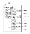
- FIG. 3 is a block diagram showing a main configuration of the microcomputer 23.
- the microcomputer 23 has an A / D conversion unit 50, 51, 52, an output unit 53, 54, a switching unit 55, an input unit 56, 57, 58, 59, a storage unit 60, and a control unit 61.
- the A / D conversion units 50, 51, 52, the output units 53, 54, the switching unit 55, the input unit 56, the storage unit 60, and the control unit 61 are connected to the internal bus 62.
- the A / D conversion units 50, 51, and 52 are further connected to the input units 57, 58, and 59, respectively.
- Each of the input units 57, 58, and 59 is connected to the power supply detection unit 22, one end of the current resistor 25, and the voltage detection unit 31.
- the output unit 53 is further connected to the drive circuit 24.
- the switching unit 55 is connected to the base of the switching switch 27 via a switch resistor 28.
- Analog power supply voltage information is input from the power supply detection unit 22 to the input unit 57.
- the input unit 57 outputs the input analog power supply voltage information to the A / D conversion unit 50.
- the A / D conversion unit 50 converts the analog power supply voltage information input from the input unit 57 into digital power supply voltage information.
- the control unit 61 acquires digital power supply voltage information from the A / D conversion unit 50.
- the power supply voltage indicated by the power supply voltage information acquired by the control unit 61 substantially matches the power supply voltage detected by the power supply detection unit 22 at the time of acquisition.
- the output unit 53 outputs an on instruction and an off instruction to the drive circuit 24 according to the instruction of the control unit 61.
- the drive circuit 24 switches the main switch 20 on when an on instruction is input, and switches the main switch 20 off when an off instruction is input.
- Analog current information is input to the input unit 58 from one end of the current resistor 25.
- the input unit 58 outputs the input analog current information to the A / D conversion unit 51.
- the A / D conversion unit 51 converts the analog current information input from the input unit 58 into digital current information.
- the control unit 61 acquires digital current information from the A / D conversion unit 51.
- the switch current indicated by the current information acquired by the control unit 61 substantially matches the switch current detected at the time of acquisition.
- the control unit 61 instructs the switching unit 55 to switch the sub switch 40 on or off.
- the switching unit 55 raises the base voltage of the changeover switch 27 with reference to the ground potential and switches the changeover switch 27 on.
- the control unit 61 instructs the sub switch 40 to switch off
- the switching unit 55 lowers the voltage of the base of the changeover switch 27 with reference to the ground potential, and switches the changeover switch 27 to off.
- the changeover switch 27 is switched off, the sub switch 40 is switched off.
- Analog node voltage information is input from the voltage detection unit 31 to the input unit 59.
- the input unit 59 outputs the input analog node voltage information to the A / D conversion unit 52.
- the A / D conversion unit 52 converts the analog node voltage information input from the input unit 59 into digital node voltage information.
- the control unit 61 acquires digital node voltage information from the A / D conversion unit 52.
- the node voltage indicated by the node voltage information acquired by the control unit 61 substantially matches the node voltage detected by the power supply detection unit 22 at the time of acquisition.
- the operation signal and the stop signal are input to the input unit 56.
- the input unit 56 notifies the control unit 61 of the input signal.
- the output unit 54 outputs a notification signal according to the instruction of the control unit 61.
- the storage unit 60 is a non-volatile memory.
- the computer program P is stored in the storage unit 60.
- the control unit 61 has a processing element for executing processing, for example, a CPU (Central Processing Unit), and functions as a processing unit.
- the processing element (computer) of the control unit 61 executes the connection detection process, the current determination process, and the power supply control process described above in parallel.
- the connection detection process is a process for detecting the connection of the load 12 to the device connector Ta.
- the current determination process is a process for determining whether or not the switch current that flows when the main switch 20 is turned on is less than the current threshold value.
- the processing element included in the control unit 61 may be readablely stored in the storage medium E.
- the computer program P read from the storage medium E by a reading device (not shown) is written in the storage unit 60.
- the storage medium E is an optical disk, a flexible disk, a magnetic disk, a magnetic optical disk, a semiconductor memory, or the like.
- the optical disk is a CD (Compact Disc) -ROM (Read Only Memory), a DVD (Digital Versatile Disc) -ROM, or a BD (Blu-ray (registered trademark) Disc).
- the magnetic disk is, for example, a hard disk.
- the computer program P may be downloaded from an external device (not shown) connected to a communication network (not shown), and the downloaded computer program P may be written in the storage unit 60.
- the number of processing elements included in the control unit 61 is not limited to 1, and may be 2 or more.
- the plurality of processing elements may jointly execute the connection detection process, the current determination process, and the power supply control process according to the computer program P.
- the storage unit 60 stores the values of the connection flag and the permission flag in addition to the computer program P.
- the values of the connection flag and the permission flag are zero or one, respectively.
- a value of the connection flag of zero means that the load 12 is not connected to the device connector Ta.
- the value of the connection flag is 1 it means that the load 12 is connected to the device connector Ta.
- the value of the permission flag is zero, it means that the main switch 20 is prohibited from being switched on.
- the value of the permission flag is 1, it means that the main switch 20 is allowed to be switched on.
- FIG. 4 is a flowchart showing the procedure of the connection detection process.
- the control unit 61 periodically executes the connection detection process when the sub switch 40 is off.
- the control unit 61 determines whether or not the main switch 20 is off (step S1).
- step S1 when the latest instruction output by the output unit 53 is an off instruction, the control unit 61 determines that the main switch 20 is off.
- the control unit 61 determines that the main switch 20 is on.
- control unit 61 determines that the main switch 20 is off (S1: YES)
- the control unit 61 acquires node voltage information from the A / D conversion unit 52 (step S2).
- the control unit 61 determines whether or not the load 12 is connected to the device connector Ta based on the node voltage indicated by the node voltage information acquired in step S2 (step S3).
- the control unit 61 determines that the load 12 is not connected when the node voltage is equal to or higher than the voltage threshold value.
- the control unit 61 determines that the load 12 is connected.
- step S4 When the control unit 61 determines that the load 12 is connected (S3: YES), the control unit 61 sets the value of the connection flag to 1 (step S4), and ends the connection detection process. If the value of the connection flag is 1 when it is determined that the control unit 61 and the load 12 are connected, the execution of step S4 is omitted, and the connection detection process ends.
- control unit 61 determines that the load 12 is not connected (S3: NO)
- the control unit 61 sets the value of the connection flag to zero (step S5), and ends the connection detection process. If the value of the connection flag is zero when the load 12 is determined not to be connected, the control unit 61 omits the execution of step S5 and ends the connection detection process.
- step S6 When the control unit 61 determines that the main switch 20 is not off, that is, the main switch 20 is on (S1: NO), the control unit 61 acquires current information from the A / D conversion unit 51 (step S6). Next, the control unit 61 determines whether or not the load 12 is connected to the device connector Ta based on the switch current indicated by the current information acquired in step S6 (step S7). As described in the operation example of the switch device 10, in step S7, when the switch current exceeds zero A, the control unit 61 determines that the load 12 is connected. When the switch current is zero A, the control unit 61 determines that the load 12 is not connected.
- the output unit 53 does not output the ON instruction to the drive circuit 24. Therefore, the drive circuit 24 switches the main switch 20 on while the value of the connection flag is 1. When the main switch 20 is on, the value of the connection flag is 1. The value of the connection flag is 1 when step S7 is executed.
- control unit 61 determines that the load 12 is not connected (S7: NO)
- the control unit 61 instructs the output unit 53 to switch the main switch 20 off (step S8).
- the output unit 53 switches the main switch 20 off by outputting an off instruction to the drive circuit 24.
- the control unit 61 sets the value of the connection flag to zero (step S9).
- the control unit 61 ends the connection detection process when it determines that the load 12 is connected (S7: YES) or after executing step S9.
- the control unit 61 detects the connection of the load 12 based on the node voltage when the main switch 20 is off, and based on the switch current when the main switch 20 is on. Detects the connection of the load 12.
- the drive circuit 24 switches the main switch 20 off, and the control unit 61 sets the value of the connection flag to zero. If the load 12 and the device connector Ta are disconnected while the load 12 is operating, the state of the switch device 10 is that the load 12 is not connected even though the main switch 20 is on. Become.
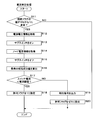
- FIG. 5 is a flowchart showing the procedure of the current determination process.
- the control unit 61 periodically executes the current determination process when the main switch 20 is off.
- the control unit 61 determines whether or not the value of the connection flag has been changed from zero to 1, that is, whether or not the load 12 is connected to the device connector Ta (step S11).
- step S11 when the value of the connection flag, which was zero at the start of the previous current determination process, is changed to 1, the control unit 61 determines that the value of the connection flag has been changed from zero to 1.
- control unit 61 determines that the value of the connection flag has not been changed from zero to one (S11: NO)
- the control unit 61 ends the current determination process.
- the control unit 61 executes the current determination process again. Therefore, when the control unit 61 determines that the value of the connection flag has not been changed from zero to 1, it waits until the value of the connection flag is changed from zero to one.
- control unit 61 determines that the value of the connection flag is changed from zero to 1, that is, the load 12 is connected to the device connector Ta (S11: YES), the control unit 61 outputs the power supply voltage information from the A / D conversion unit 50. Acquire (step S12). Next, the control unit 61 instructs the switching unit 55 to switch the sub switch 40 on (step S13). As described above, the switching unit 55 switches the sub switch 40 on by switching the switching switch 27 on. When the sub switch 40 is switched on, the capacitor 30 is charged until the node voltage becomes the first voltage dividing voltage.
- step S14 the control unit 61 acquires node voltage information from the A / D conversion unit 52 (step S14).
- the period from the end of the execution of step S13 to the start of the execution of step S14 is longer than the period from when the sub switch 40 is switched on to when the charging of the capacitor 30 is completed. Therefore, the node voltage indicated by the node voltage information acquired by the control unit 61 in step S14 is the first voltage dividing voltage.
- step S15 the control unit 61 instructs the switching unit 55 to switch the sub switch 40 off (step S15).
- the switching unit 55 switches the sub switch 40 off by switching the switching switch 27 off.
- the capacitor 30 is discharged and the node voltage drops to the second voltage dividing voltage.
- step S15 the control unit 61 calculates the resistance component value of the load 12 based on the node voltage indicated by the node voltage information acquired in step S14, that is, the first voltage dividing voltage (step S16). Next, the control unit 61 determines whether or not the switch current flowing when the main switch 20 is switched on is less than the current threshold value based on the resistance component value calculated in step S16 (step S17). ..
- step S17 the control unit 61 calculates the switch current based on the power supply voltage indicated by the power supply voltage information acquired in step S12 and the resistance component value calculated in step S16. The control unit 61 determines whether or not the calculated switch voltage is less than the current threshold value.
- step S17 when the resistance component value calculated in step S16 is equal to or greater than the resistance threshold value, the control unit 61 determines that the switch current is less than the current threshold value. When the resistance component value calculated in step S16 is less than the resistance threshold value, the control unit 61 determines that the switch current is equal to or more than the current threshold value.
- the resistance threshold is a constant value and is preset.
- control unit 61 determines that the switch current is less than the current threshold value (S17: YES)
- the control unit 61 sets the value of the permission flag to 1 (step S18), and ends the current determination process.
- the control unit 61 determines that the switch current is equal to or greater than the current threshold value (S17: NO)
- the control unit 61 instructs the output unit 54 to output a notification signal indicating that power supply to the load 12 is impossible (S17: NO). Step S19).
- the control unit 61 sets the value of the permission flag to zero (step S20), and ends the current determination process.
- the resistance component value of the load 12 is calculated, and whether or not the switch current is less than the current threshold value based on the calculated resistance component value. Is determined.
- the control unit 61 determines that the switch current is less than the current threshold value, the control unit 61 sets the value of the permission flag to 1 and permits the main switch 20 to be switched on.
- FIG. 6 is a flowchart showing the procedure of the power supply control process.
- the control unit 61 periodically executes the power supply control process when the sub switch 40 is off.
- the control unit 61 determines whether or not an operation signal has been input to the input unit 56 (step S31).
- the control unit 61 determines whether or not a stop signal has been input to the input unit 56 (step S32).
- the control unit 61 ends the power supply control process.
- the control unit 61 executes the power supply control process again. Therefore, when the operation signal or the stop signal is not input to the input unit 56, the control unit 61 waits until the operation signal or the stop signal is input to the input unit 56.
- control unit 61 determines whether or not the value of the connection flag is 1 (step S33).
- control unit 61 determines whether or not the value of the permission flag is 1 (step S34).
- control unit 61 instructs the output unit 53 to turn on the main switch 20 (step S35).
- the output unit 53 switches the main switch 20 on by outputting an ON instruction to the drive circuit 24. As a result, the load 12 operates.
- the control unit 61 determines that the value of the connection flag is not 1 (S33: NO) or determines that the value of the permission flag is not 1 (S34: NO), the control unit 61 instructs the output unit 54.
- the notification signal is output (step S36). If the value of the connection flag is not 1, the output unit 54 outputs a notification signal indicating that the load 12 is not connected. If the value of the permission flag is not 1, the output unit 54 outputs a notification signal indicating that power cannot be supplied to the load 12.
- steps S35 and S36 is executed, the control unit 61 ends the power supply control process.
- step S37 the control unit 61 instructs the output unit 53 to switch the main switch 20 off.
- the output unit 53 switches the main switch 20 off by outputting an off instruction to the drive circuit 24.
- the load 12 stops operating.
- step S37 the control unit 61 ends the power supply control process.
- the control unit 61 instructs the output unit 53 to switch the main switch 20 on.
- the value of the permission flag is zero, the control unit 61 does not instruct the output unit 53 to switch the main switch 20 on. Therefore, the passage of an overcurrent exceeding the current threshold value is prevented.
- the control unit 61 instructs the output unit 53 to switch the main switch 20 off.
- FIG. 7 is a block diagram showing a main configuration of the microcomputer 23 according to the second embodiment.
- the microcomputer 23 in the second embodiment has a clock signal output unit 63 in addition to the components included in the microcomputer 23 in the first embodiment.
- the clock signal output unit 63 is connected to the internal bus 62 and directly connected to the control unit 61.
- the clock signal output unit 63 outputs a clock signal to the control unit 61.
- the clock signal is composed of a high level voltage and a low level voltage.
- the voltage indicated by the clock signal periodically switches from the low level voltage to the high level voltage.
- the processing element of the control unit 61 executes one process each time the voltage is switched from the low level voltage to the high level voltage in the clock signal.
- the control unit 61 stops the output of the clock signal to the clock signal output unit 63 via the internal bus 62.
- the processing element of the control unit 61 stops operating.
- the operation signal and stop signal are input not only to the input unit 56 but also to the clock signal output unit 63.
- the clock signal output unit 63 restarts the output of the clock signal to the control unit 61.
- the processing element of the control unit 61 resumes operation.
- the processing element of the control unit 61 executes not only the connection detection process, the current determination process, and the power supply control process, but also the pause process and the start process.
- the pause process is a process of stopping the output of the clock signal.
- the start-up process is the first process to be executed when the control unit 61 resumes operation.
- FIG. 8 is a flowchart showing the procedure of the pause process.
- the control unit 61 periodically executes the pause process.
- the control unit 61 determines whether or not to pause the operation (step S41).
- the control unit 61 determines that the operation is suspended when the off period in which the main switch 20 and the sub switch 40 are off is equal to or longer than the reference period. When the off period is less than the reference time, the control unit 61 determines that the operation is not paused.
- control unit 61 determines that the operation is not paused (S41: NO)
- the control unit 61 ends the pause processing.
- the control unit 61 executes the pause process. Therefore, when the control unit 61 determines that the operation is not paused, the control unit 61 waits until the off period becomes equal to or longer than the reference period.
- the control unit 61 determines that the operation is suspended (S41: YES)
- the control unit 61 instructs the clock signal output unit 63 to stop the output of the clock signal to the control unit 61 (step S42), and ends the pause process. ..
- the control unit 61 suspends the operation. If an operation signal or a stop signal is input to the clock signal output unit 63 after the control unit 61 has stopped operating, the clock signal output unit 63 resumes the output of the clock signal, and the control unit 61 resumes the operation. ..
- FIG. 9 is a flowchart showing the procedure of the start-up process.
- the control unit 61 executes the start-up process when the operation is restarted, that is, when the output of the clock signal is restarted. Since the control unit 61 pauses in a state where the main switch 20 and the sub switch 40 are off, the start-up process is executed in a state where the main switch 20 and the sub switch 40 are off. A part of the start-up process is the same as a part of the current determination process. Therefore, regarding the start-up process, a process similar to a part of the current determination process, that is, the description of steps S12 to S20 will be omitted.
- the control unit 61 acquires the node voltage information from the A / D conversion unit 52 (step S51). Next, the control unit 61 determines whether or not the load 12 is connected to the device connector Ta based on the node voltage indicated by the node voltage information acquired in step S51, as in step S3 of the connection detection process. (Step S52).
- control unit 61 determines that the load 12 is not connected (S52: NO)
- the control unit 61 sets the value of the connection flag to zero (step S53), and ends the start-up process.
- the control unit 61 determines that the load 12 is connected (S52: YES)
- the control unit 61 sets the value of the connection flag to 1 (step S54).
- step S54 the control unit 61 sequentially executes steps S12 to S16 to calculate the resistance component value of the load 12. Based on the calculated resistance component value, the control unit 61 determines whether or not the switch current that flows when the main switch 20 is switched on is less than the current threshold value. The control unit 61 sets the value of the permission flag to zero or one according to the determination result.
- the control unit 61 ends the start-up process after executing one of steps S18 and S20. After finishing the start-up process, the control unit 61 executes the connection detection process, the current determination process, the power supply control process, and the pause process.
- the control unit 61 determines whether or not the load 12 is connected to the device connector Ta.
- the control unit 61 calculates the resistance component value of the load 12, and based on the calculated resistance component value, the switch current that flows when the main switch 20 is switched on. Determines if is less than the current threshold. Therefore, when the electric device connected to the device connector Ta is changed to the electric device having a small resistance component value as the load 12 while the control unit 61 is inactive, the control unit 61 is erroneously used. Therefore, the output unit 53 is not instructed to switch the main switch 20 on.
- the switch device 10 according to the second embodiment similarly exhibits the effect of the switch device 10 according to the first embodiment.
- control unit 61 may omit step S12 in the current determination process in the first and second embodiments. In this case, in step S16, the control unit 61 uses a preset value as the power supply voltage.
- step S17 of the current determination process in the first and second embodiments the control unit 61 determines whether or not the switch current is less than the current threshold value based on the resistance component value calculated in step S16. However, in step S17, the control unit 61 directly determines whether or not the switch current is less than the current threshold value based on the node voltage indicated by the node voltage information acquired in step S14, that is, the first voltage dividing voltage. You may. As described above, the switch current that flows when the main switch 20 is switched on increases as the resistance component value of the load 12 decreases. The resistance component value of the load 12 becomes smaller as the first voltage dividing voltage is lower. Therefore, the lower the first voltage dividing voltage, the larger the switch current.
- step S17 the control unit 61 determines that the switch current is equal to or greater than the current threshold value when the node voltage indicated by the node voltage information acquired in step S14 is less than the reference voltage.
- the control unit 61 determines that the switch current is less than the current threshold value.
- the first voltage dividing voltage is proportional to the power supply voltage of the DC power supply 11. Therefore, the reference voltage used in step S17 is changed according to the power supply voltage indicated by the power supply voltage information acquired in step S12.
- control unit 61 does not need to change the reference voltage. In this case, in the current determination process, the control unit 61 may omit step S12. Further, the switch device 10 does not need to have the power supply detection unit 22, and the microcomputer 23 does not need to have the A / D conversion unit 50 and the input unit 57.
- the control unit 61 may omit the execution of step S12 as in the current determination process. Further, in step S17 of the start-up process, the control unit 61 performs the switch current based on the node voltage indicated by the node voltage information acquired in step S14, that is, the first voltage dividing voltage, as in step S17 of the current determination process. May be directly determined whether or not is less than the current threshold.
- the method of stopping the operation of the control unit 61 is not limited to the method of stopping the output of the clock signal.
- the period of the clock signal output by the clock signal output unit 63 to the control unit 61 that is, the interval at which the low level voltage is switched to the high level voltage is described as the first period.
- the control unit 61 operates by instructing the clock signal output unit 63 to change the cycle of the clock signal output to the control unit 61 from the first cycle to the second cycle longer than the first cycle. May be paused.
- the operation signal and the stop signal are not input to the clock signal output unit 63.
- the control unit 61 determines whether or not an operation signal or a stop signal is input to the input unit 56 each time the clock signal voltage is switched from the low level voltage to the high level voltage while the clock signal cycle is the second cycle. judge.
- the control unit 61 instructs the clock signal output unit 63 to change the clock signal cycle to the first cycle and execute the start processing.
- the clock signal is not limited to a signal in which the voltage periodically switches from the low level voltage to the high level voltage, and may be a signal in which the voltage periodically switches from the high level voltage to the low level voltage.
- the processing element of the control unit 61 executes processing each time the voltage is switched from the high level voltage to the low level voltage in the clock signal.
- the subswitch 40 of the switch circuit 26 is not limited to the P-channel type FET.
- the third embodiment will be described as different from the first embodiment.
- Other configurations except the configuration described later are common to the first embodiment. Therefore, the same reference reference numerals as those in the first embodiment are assigned to the components common to the first embodiment, and the description thereof will be omitted.
- FIG. 10 is a block diagram showing a main configuration of the switch device 10 according to the third embodiment.
- the switch device 10 according to the third embodiment also has other components other than the changeover switch 27 and the switch resistor 28 among the components included in the switch device 10 according to the first embodiment.
- the switch device 10 in the third embodiment further includes a drive circuit 32.
- the switch circuit 26 in the third embodiment has a series resistor 43 in addition to the components of the switch circuit 26 in the first embodiment.
- the sub-switch 40 in the third embodiment is an N-channel type FET.
- the drain of the sub switch 40 of the switch circuit 26 is connected to the drain of the main switch 20.
- the source of the subswitch 40 is connected to one end of the series resistor 43.
- the series resistor 43 functions as a second resistor.
- the other end of the series resistor 43 is connected to a connection node between the current output circuit 21 and the device connector Ta.
- a switch resistor 41 is connected between the gate and the source of the sub switch 40.
- the gate of the subswitch 40 is further connected to one end of the switch resistor 42.
- the other end of the switch resistor 42 is connected to the drive circuit 32.
- the drive circuit 32 is further connected to the switching unit 55 of the microcomputer 23.
- the sub switch 40 when the gate voltage based on the source potential is a certain voltage or more, the resistance value between the drain and the source is sufficiently small. At this time, the sub switch 40 is on, and current can flow through the drain and the source. In the subswitch 40, when the gate voltage with respect to the source potential is less than a constant voltage, the resistance value between the drain and the source is sufficiently large. At this time, the sub switch 40 is off, and no current flows through the drain and the source.
- the switching unit 55 when the control unit 61 instructs the switching unit 55 to switch the sub switch 40 on, the switching unit 55 outputs a second on instruction instructing the sub switch 40 to switch on.
- the drive circuit 32 raises the voltage of the gate of the subswitch 40 with reference to the ground potential.
- the voltage of the gate based on the potential of the source becomes a constant voltage or more, and the sub switch 40 is switched on.
- the switching unit 55 when the control unit 61 instructs the switching unit 55 to switch the sub switch 40 to off, the switching unit 55 outputs a second off instruction instructing the switching of the sub switch 40 to off.
- the drive circuit 32 lowers the voltage at the gate of the subswitch 40 with reference to the ground potential.
- the voltage of the gate based on the potential of the source becomes less than a constant voltage, and the sub switch 40 is switched off.
- the on-resistance value of the N-channel FET is usually several ohms and is small.
- a series resistor 43 is connected in series to the sub switch 40 in order to realize a circuit having a large resistance value when the sub switch 40 is on. For example, when the resistance value of the series resistor 43 is several hundred ohms, the resistance value of the switch circuit 26 when the sub switch 40 is on is several hundred ohms.
- the resistance value of the switch circuit 26 when the sub switch 40 is on is larger than the on resistance value of the main switch 20.
- the resistance value of the circuit resistance is larger than the resistance value of the switch circuit 26 when the sub switch 40 is on.
- the current flowing when the load 12 having a resistance component value of zero ohm is connected to the device connector Ta and the main switch 20 and the sub switch 40 are off and on, respectively, is a normal value that does not cause smoke generation.
- the switch device 10 in the third embodiment similarly exhibits the effect of the switch device 10 in the first embodiment.
- the on-resistance value of the relay contact is smaller than the on-resistance value of the N-channel FET. Therefore, a relay contact may be used as the sub switch 40 in the third embodiment.
- the switch device 10 is provided with a configuration for switching the sub switch 40 on or off.
- the sub switch 40 is switched on or off by the switching unit 55.
- the source of the sub switch 40 may be connected to the connection node between the current output circuit 21 and the device connector Ta.
- one end of the series resistor 43 may be connected in series to the drain of the sub switch 40.
- the other end of the series resistor 43 is connected to the connection node between the current output circuit 21 and the device connector Ta.
- the switch device 10 in the second embodiment may be configured in the same manner as the switch device 10 in the third embodiment.
- the sub switch 40 is not limited to the FET or the relay contact, and may be a switch such as a bipolar transistor or an IGBT (Insulated Gate Bipolar Transistor).
- the configuration for detecting the switch current is not limited to the configuration in which a current that is a predetermined fraction of the switch current is output to the current resistor 25, and a configuration using a shunt resistor or a current sensor may be used.
- the shunt resistor is connected in series with the source of the main switch 20, and the switch current is detected based on the voltage between both ends of the shunt resistor.
- the current sensor detects the switch current based on the strength of the magnetic field generated when the switch current flows through the connection line connected to the source of the main switch 20.
Landscapes
- Engineering & Computer Science (AREA)
- Power Engineering (AREA)
- Direct Current Feeding And Distribution (AREA)
- Electronic Switches (AREA)
Priority Applications (2)
| Application Number | Priority Date | Filing Date | Title |
|---|---|---|---|
| CN202080081428.7A CN114731041B (zh) | 2019-12-13 | 2020-11-26 | 开关装置、电流判定方法和计算机程序 |
| US17/784,823 US12531426B2 (en) | 2019-12-13 | 2020-11-26 | Switch device, current determination method and computer program |
Applications Claiming Priority (2)
| Application Number | Priority Date | Filing Date | Title |
|---|---|---|---|
| JP2019-225848 | 2019-12-13 | ||
| JP2019225848A JP7196826B2 (ja) | 2019-12-13 | 2019-12-13 | スイッチ装置、電流判定方法及びコンピュータプログラム |
Publications (1)
| Publication Number | Publication Date |
|---|---|
| WO2021117492A1 true WO2021117492A1 (ja) | 2021-06-17 |
Family
ID=76328951
Family Applications (1)
| Application Number | Title | Priority Date | Filing Date |
|---|---|---|---|
| PCT/JP2020/043937 Ceased WO2021117492A1 (ja) | 2019-12-13 | 2020-11-26 | スイッチ装置、電流判定方法及びコンピュータプログラム |
Country Status (4)
| Country | Link |
|---|---|
| US (1) | US12531426B2 (https=) |
| JP (1) | JP7196826B2 (https=) |
| CN (1) | CN114731041B (https=) |
| WO (1) | WO2021117492A1 (https=) |
Families Citing this family (1)
| Publication number | Priority date | Publication date | Assignee | Title |
|---|---|---|---|---|
| JP2023148451A (ja) * | 2022-03-30 | 2023-10-13 | 古河電気工業株式会社 | 保護装置 |
Citations (3)
| Publication number | Priority date | Publication date | Assignee | Title |
|---|---|---|---|---|
| JP2018011411A (ja) * | 2016-07-13 | 2018-01-18 | 株式会社オートネットワーク技術研究所 | 電力供給制御装置 |
| WO2019054138A1 (ja) * | 2017-09-15 | 2019-03-21 | 株式会社村田製作所 | 蓄電装置用昇降圧装置及び蓄電装置 |
| JP2019205252A (ja) * | 2018-05-22 | 2019-11-28 | 矢崎総業株式会社 | 電力配電システム |
Family Cites Families (3)
| Publication number | Priority date | Publication date | Assignee | Title |
|---|---|---|---|---|
| JP6365497B2 (ja) * | 2015-10-14 | 2018-08-01 | 株式会社オートネットワーク技術研究所 | 電流制御装置、電流制御方法及びコンピュータプログラム |
| JP6620674B2 (ja) * | 2016-05-26 | 2019-12-18 | 株式会社オートネットワーク技術研究所 | 給電制御装置、給電制御方法及びコンピュータプログラム |
| JP6958418B2 (ja) * | 2018-02-21 | 2021-11-02 | 株式会社オートネットワーク技術研究所 | 給電制御装置 |
-
2019
- 2019-12-13 JP JP2019225848A patent/JP7196826B2/ja active Active
-
2020
- 2020-11-26 US US17/784,823 patent/US12531426B2/en active Active
- 2020-11-26 WO PCT/JP2020/043937 patent/WO2021117492A1/ja not_active Ceased
- 2020-11-26 CN CN202080081428.7A patent/CN114731041B/zh active Active
Patent Citations (3)
| Publication number | Priority date | Publication date | Assignee | Title |
|---|---|---|---|---|
| JP2018011411A (ja) * | 2016-07-13 | 2018-01-18 | 株式会社オートネットワーク技術研究所 | 電力供給制御装置 |
| WO2019054138A1 (ja) * | 2017-09-15 | 2019-03-21 | 株式会社村田製作所 | 蓄電装置用昇降圧装置及び蓄電装置 |
| JP2019205252A (ja) * | 2018-05-22 | 2019-11-28 | 矢崎総業株式会社 | 電力配電システム |
Also Published As
| Publication number | Publication date |
|---|---|
| JP7196826B2 (ja) | 2022-12-27 |
| US20230008237A1 (en) | 2023-01-12 |
| JP2021097453A (ja) | 2021-06-24 |
| CN114731041A (zh) | 2022-07-08 |
| US12531426B2 (en) | 2026-01-20 |
| CN114731041B (zh) | 2025-08-05 |
Similar Documents
| Publication | Publication Date | Title |
|---|---|---|
| WO2017065055A1 (ja) | 電流制御装置、電流制御方法及びコンピュータプログラム | |
| US20180358806A1 (en) | Power supply control apparatus | |
| JP6620674B2 (ja) | 給電制御装置、給電制御方法及びコンピュータプログラム | |
| CN110021971B (zh) | 供电控制装置及供电控制方法 | |
| JP2019169873A (ja) | 制御装置、制御方法及びコンピュータプログラム | |
| JP7067033B2 (ja) | 給電制御装置、給電制御方法及びコンピュータプログラム | |
| JP5163211B2 (ja) | リセット回路および電源制御用半導体集積回路 | |
| WO2021117492A1 (ja) | スイッチ装置、電流判定方法及びコンピュータプログラム | |
| WO2019155890A1 (ja) | 給電制御装置、給電制御方法及びコンピュータプログラム | |
| CN112582985B (zh) | 电子设备 | |
| CN108292851A (zh) | 供电控制装置 | |
| US11870427B2 (en) | Power supply control device | |
| JP4148243B2 (ja) | 異常検出回路 | |
| JP2014092712A (ja) | 残留電荷除去装置、画像処理装置、残留電荷除去方法及び残留電荷除去プログラム | |
| JP7404985B2 (ja) | 給電制御装置、検査方法及びコンピュータプログラム | |
| US12176165B2 (en) | Slow-release relay circuit and train control device | |
| WO2018168392A1 (ja) | 給電制御装置、給電制御方法及びコンピュータプログラム | |
| JP2007193458A (ja) | 電源回路 | |
| JP2024089201A (ja) | 電子制御装置 | |
| KR20230099945A (ko) | 가스 경보 장치 | |
| JP2018006815A (ja) | 出力装置及び切替えシステム |
Legal Events
| Date | Code | Title | Description |
|---|---|---|---|
| 121 | Ep: the epo has been informed by wipo that ep was designated in this application |
Ref document number: 20898133 Country of ref document: EP Kind code of ref document: A1 |
|
| NENP | Non-entry into the national phase |
Ref country code: DE |
|
| 122 | Ep: pct application non-entry in european phase |
Ref document number: 20898133 Country of ref document: EP Kind code of ref document: A1 |
|
| WWG | Wipo information: grant in national office |
Ref document number: 202080081428.7 Country of ref document: CN |
|
| WWG | Wipo information: grant in national office |
Ref document number: 17784823 Country of ref document: US |