WO2021111573A1 - リザーバ計算データフロープロセッサ - Google Patents
リザーバ計算データフロープロセッサ Download PDFInfo
- Publication number
- WO2021111573A1 WO2021111573A1 PCT/JP2019/047549 JP2019047549W WO2021111573A1 WO 2021111573 A1 WO2021111573 A1 WO 2021111573A1 JP 2019047549 W JP2019047549 W JP 2019047549W WO 2021111573 A1 WO2021111573 A1 WO 2021111573A1
- Authority
- WO
- WIPO (PCT)
- Prior art keywords
- reservoir
- data flow
- input
- output
- unit
- Prior art date
- Legal status (The legal status is an assumption and is not a legal conclusion. Google has not performed a legal analysis and makes no representation as to the accuracy of the status listed.)
- Ceased
Links
Images




Classifications
-
- G—PHYSICS
- G06—COMPUTING OR CALCULATING; COUNTING
- G06F—ELECTRIC DIGITAL DATA PROCESSING
- G06F15/00—Digital computers in general; Data processing equipment in general
- G06F15/76—Architectures of general purpose stored program computers
- G06F15/82—Architectures of general purpose stored program computers data or demand driven
- G06F15/825—Dataflow computers
-
- E—FIXED CONSTRUCTIONS
- E21—EARTH OR ROCK DRILLING; MINING
- E21B—EARTH OR ROCK DRILLING; OBTAINING OIL, GAS, WATER, SOLUBLE OR MELTABLE MATERIALS OR A SLURRY OF MINERALS FROM WELLS
- E21B41/00—Equipment or details not covered by groups E21B15/00 - E21B40/00
-
- G—PHYSICS
- G06—COMPUTING OR CALCULATING; COUNTING
- G06F—ELECTRIC DIGITAL DATA PROCESSING
- G06F30/00—Computer-aided design [CAD]
- G06F30/20—Design optimisation, verification or simulation
-
- G—PHYSICS
- G06—COMPUTING OR CALCULATING; COUNTING
- G06N—COMPUTING ARRANGEMENTS BASED ON SPECIFIC COMPUTATIONAL MODELS
- G06N3/00—Computing arrangements based on biological models
- G06N3/02—Neural networks
- G06N3/04—Architecture, e.g. interconnection topology
- G06N3/044—Recurrent networks, e.g. Hopfield networks
-
- G—PHYSICS
- G06—COMPUTING OR CALCULATING; COUNTING
- G06N—COMPUTING ARRANGEMENTS BASED ON SPECIFIC COMPUTATIONAL MODELS
- G06N3/00—Computing arrangements based on biological models
- G06N3/02—Neural networks
- G06N3/06—Physical realisation, i.e. hardware implementation of neural networks, neurons or parts of neurons
- G06N3/063—Physical realisation, i.e. hardware implementation of neural networks, neurons or parts of neurons using electronic means
-
- G—PHYSICS
- G06—COMPUTING OR CALCULATING; COUNTING
- G06N—COMPUTING ARRANGEMENTS BASED ON SPECIFIC COMPUTATIONAL MODELS
- G06N3/00—Computing arrangements based on biological models
- G06N3/02—Neural networks
- G06N3/10—Interfaces, programming languages or software development kits, e.g. for simulating neural networks
- G06N3/105—Shells for specifying net layout
-
- E—FIXED CONSTRUCTIONS
- E21—EARTH OR ROCK DRILLING; MINING
- E21B—EARTH OR ROCK DRILLING; OBTAINING OIL, GAS, WATER, SOLUBLE OR MELTABLE MATERIALS OR A SLURRY OF MINERALS FROM WELLS
- E21B2200/00—Special features related to earth drilling for obtaining oil, gas or water
- E21B2200/20—Computer models or simulations, e.g. for reservoirs under production, drill bits
-
- E—FIXED CONSTRUCTIONS
- E21—EARTH OR ROCK DRILLING; MINING
- E21B—EARTH OR ROCK DRILLING; OBTAINING OIL, GAS, WATER, SOLUBLE OR MELTABLE MATERIALS OR A SLURRY OF MINERALS FROM WELLS
- E21B2200/00—Special features related to earth drilling for obtaining oil, gas or water
- E21B2200/22—Fuzzy logic, artificial intelligence, neural networks or the like
-
- G—PHYSICS
- G06—COMPUTING OR CALCULATING; COUNTING
- G06F—ELECTRIC DIGITAL DATA PROCESSING
- G06F2111/00—Details relating to CAD techniques
- G06F2111/10—Numerical modelling
Definitions
- the present invention relates to a reservoir calculation data flow processor.
- the time series signal is stream data that changes from moment to moment.
- Examples of the time-series signal include a signal corresponding to sensor data indicating the status of equipment and processes operating in a factory, a biological signal obtained from a wearable device, and the like. By measuring and analyzing such time-series signals, it is possible to obtain a sign of a mechanical failure or a biological disease.
- the architecture of the neural network to be trained is represented by a data flow graph, and the calculation is streamlined. For example, weighting is performed by automatic differentiation. It has been proposed to update the parameters efficiently.
- a recursive architecture such as LSTM or GRU
- the data flow processors for machine learning that have been proposed so far are mainly for deep learning of hierarchical architecture (convolution calculation of the deep learning), and are for time-series learning. Few have been proposed.
- Non-Patent Document 1 shows that, from a theoretical standpoint, a reservoir of a one-dimensional ring topology and an interconnected reservoir having a specific weight parameter distribution are mathematically equivalent (Non-Patent Document 1). See 1.).
- Non-Patent Document 2 and Non-Patent Document 3 propose techniques that extend the theoretical analysis in Non-Patent Document 1 (see Non-Patent Document 2-3).
- Non-Patent Document 2 and Non-Patent Document 3 it is assumed that the physical implementation is implemented by a Delay-time Reservoir having a one-dimensional ring topology configuration.
- Such a one-dimensional ring topology reservoir has an architecture suitable for implementation with fast-moving optical lasers.
- Non-Patent Document 1 when the reservoir (intermediate layer) is physically mounted, it is not assumed that the architecture has an interconnected configuration.
- a virtual node is introduced and sequential nonlinear operations are performed by time division to realize a reservoir calculation that is mathematically equivalent to a reservoir having a specific interconnect configuration.
- the operation equation of the virtual node in the reservoir is derived, it is not considered to integrate and implement the operation equation as FPGA or ASIC of the two-dimensional array.
- the present invention has been made to solve such a problem, and an object of the present invention is to provide a reservoir calculation data flow processor which is a device dedicated to reservoir calculation suitable for configuring a reservoir.
- One aspect of the present invention includes a plurality of reservoir units as units constituting the reservoir, and the reservoir can be reconfigured by changing the connection relationship between the reservoir units, and the reservoir unit can perform a predetermined calculation.
- the calculation unit block includes a first addition unit that adds at least two inputs, and an output from the first addition unit or the result of multiplying the output by a predetermined coefficient and a non-linear function. It is a reservoir calculation data flow processor including a non-linear arithmetic unit that performs the addition of at least two inputs including an output from the non-linear arithmetic unit or the result of multiplying the output by a predetermined coefficient.
- the calculation unit block further includes a block for connecting the reservoir units and a block for performing input / output, and the reservoir calculation data flow processor. Further includes a data flow control unit that switches the connection relationship between the reservoir units.
- the reservoir calculation data flow processor can reconfigure the reservoir set by the user.
- the reservoir calculation data flow processor can reconfigure the reservoir based on predetermined information.
- the plurality of the calculation unit blocks are spatially arranged in parallel.
- the plurality of the calculation unit blocks are arranged in parallel in time.
- the first addition unit is at least temporally multiplied by a signal corresponding to the output signal from the previous second addition unit or the signal by a predetermined coefficient.
- the result is added to the input signal to the reservoir or the result of multiplying the input signal by a predetermined coefficient.
- the second addition unit is spatially arranged in parallel with at least the output from the non-linear arithmetic unit or the result of multiplying the output by a predetermined coefficient.
- the signal corresponding to the output signal from the second addition unit of the other stage of the plurality of stages or the result of multiplying the signal by a predetermined coefficient is added.
- a reservoir calculation data flow processor suitable for forming a reservoir.
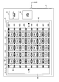
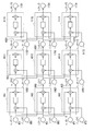
- FIG. 1 is a diagram showing a schematic configuration of a reservoir calculation data flow processor 1 according to an embodiment of the present invention. Note that FIG. 1 shows an XY coordinate system, which is a Cartesian coordinate system, for convenience of explanation.
- the reservoir calculation data flow processor 1 is an ASIC that performs digital processing.
- the reservoir calculation data flow processor 1 includes an array unit 21, a data flow control unit 22 which is an example of a control unit, and a shared storage unit 23 which is an example of a storage unit.
- the reservoir calculation data flow processor 1 may be configured not to include the shared storage unit 23.
- the reservoir calculation data flow processor 1 is connected to the input layer 41 and the output layer 42 of the reservoir calculation, respectively.
- the reservoir calculation data flow processor 1 itself does not need to include the input layer 41 and the output layer 42.
- the array unit 21 is configured as a building block (functional block) by arranging a plurality of digital reservoir units (DRU: Digital Barrel Unit) in an array, and each reservoir unit is a connection block (CB: Connecting Block). , And a functional block such as an input / output interface block (IB: I / O Interface Block).
- DRU Digital Barrel Unit
- CB Connecting Block
- IB I / O Interface Block
- the digital reservoir unit may be referred to as DRU
- the connection block may be referred to as CB
- IB input / output interface block
- the DRU is composed of a plurality of arithmetic units for executing operations corresponding to virtual nodes of the reservoir as physical nodes. These plurality of arithmetic units include arithmetic units that perform non-linear arithmetic.
- the CB has a function of receiving the state value of the DRU as an intermediate signal and bridging it as an input to different surrounding DRUs. Further, the CB has a memory function of holding the state value of each DRU at a certain time.
- the IB has a function of giving an input signal from the input layer to each DRU and passing a desired DRU state value as an output signal to the output layer.
- the IB has a function of feeding back the state value of a certain DRU at a certain time as an input to the same DRU at the next time.
- the IB may feed back the state value of a certain DRU at a certain time as an input to an arbitrary DRU after a certain time, not limited to the next time.
- a plurality of DRUs are arranged on a plane in the array unit 21.
- two directions orthogonal to each other on the plane will be referred to as a vertical direction and a horizontal direction.
- the direction parallel to the X axis is called the horizontal direction
- the direction parallel to the Y axis is called the vertical direction.
- the number of steps of the DRU in the horizontal direction increases toward the positive direction of the X-axis
- the number of steps of the DRU in the vertical direction increases toward the positive direction of the Y-axis.
- the plurality of functional blocks are arranged according to a predetermined pattern.
- one DRU is designated by the reference numeral “51 (i, j)”.
- each DRU is distinguished by notation as DRU51 (i, j).
- L is an integer of 2 or more.
- L is 7.
- k is an integer of 2 or more. In the example of FIG. 1, k is 5.
- each CB is distinguished by notation as CB111 to CB116.
- each IB is distinguished by notation as IB121 to IB128.
- CB111, CB112, CB113, CB114, CB115, and CB116 are arranged so as to arrange six functional blocks in the horizontal direction.
- the number of CBs 111 to 116 is arranged so as to be (k + 1) with respect to the number of stages (k) of the DRU51 (i, j) in the horizontal direction.
- IB121, IB122, IB123, IB124, IB125, IB126, IB127, and IB128 are arranged so as to arrange eight functional blocks in the vertical direction.
- the number of IBs 121 to 128 is arranged so as to be (L + 1) with respect to the number of stages (L) of the DRU51 (i, j) in the vertical direction.
- Each CB 111 to 116 over a plurality of stages in the vertical direction is arranged so as to intersect each IB 121 to 128 over a plurality of stages in the horizontal direction.
- the wiring connection relationship shown in FIG. 1 is a schematic example for illustration. Not limited to the example of FIG. 1, various connection relationships may be used with respect to DRU51 (i, j), CB111 to 116 and IB121 to 128. Not limited to the example of FIG. 1, in each of the functional blocks of DRU51 (i, j), CB111 to 116 and IB121 to 128, the number of terminals connected to other functional blocks may be any number. The number of wirings included in the respective CBs 111 to 116 and IBs 121 to 128 may be any number.
- the DRU51 (i, j) is connected to the adjacent CBs 111 to 116 and IBs 121 to 128 via terminals.
- Bus-type wiring is provided inside CB111 to 116 and IB121 to 128, and the intersections of IB121 to 128 and CB111 to 116 can be connected via vias.
- Each functional block of DRU51 (i, j), CB111 to 116, and IB121 to 128 has a switch, and by switching by a control signal from the data flow control unit 22, coupling between DRU51 (i, j) is performed. At the same time, the route of the input / output signal can be changed. That is, the reservoir calculation data flow processor 1 according to the present embodiment is a reconfigurable data flow processor.
- the DRU 51 (i, j) has a connection portion for each CB 111 to 116 adjacent to the DRU 51 (i, j) and a connection portion for each IB 121 to 128 adjacent to the DRU 51 (i, j).
- the DRU 51 (i, j) can be connected to the respective CB 111 to 116 via a connection portion to the respective CB 111 to 116 adjacent to the DRU 51 (i, j).
- the DRU 51 (i, j) can be connected to the respective IBs 121 to 128 via a connection portion to the respective IBs 121 to 128 adjacent to the DRU 51 (i, j).
- the connection portion 52 that can be connected to one CB 116 and the connection portion 53 that can be connected to one IB 121 are coded. is there.
- the data flow control unit 22 controls various processes and data flows.
- the data flow control unit 22 changes the wiring connection relationship for the plurality of functional blocks included in the array unit 21. Such changes may be referred to as, for example, configurable or reconfigurable. That is, the data flow control unit 22 initially configures the reservoir realized by the array unit 21 by changing the connection relationship of the plurality of functional blocks included in the array unit 21, or has already configured it. It is possible to change the existing reservoir to configure (ie, reconfigure) another reservoir.
- the data flow control unit 22 may automatically perform such a configuration (or reconstruction) based on, for example, a predetermined rule, or the content of the operation performed by the user. It may be done based on.
- the fact that such a configuration or reconstruction can be performed based on the content of the operation performed by the user may be referred to as programmable, for example. Therefore, the data flow control unit 22 has a function of storing and holding the configuration contents programmed by the user.
- the shared storage unit 23 stores various types of information, for example, the state values of the DRU 51 (i, j) at each time.
- the shared storage unit 23 is used by the data flow control unit 22 to store information as needed.
- the data flow control unit 22 performs, for example, a process of writing information to the shared storage unit 23 and a process of reading out the information stored in the shared storage unit 23.
- the array unit 21 for example, only the reservoir body (intermediate layer) may be configured, or the reservoir and other logic circuits related to the reservoir may be configured.
- the other logic circuit may be, for example, one or both of the input layer 41 for the reservoir and the output layer 42 for the reservoir.
- the array unit 21 may include a logic circuit for learning the weight parameter of the coupling from the reservoir (intermediate layer) to the output layer 42.
- the array unit 21 may include an arbitrary number of functional blocks in an arbitrary arrangement. Further, the array unit 21 may be provided with an arbitrary number of wires in an arbitrary arrangement. Then, the array unit 21 may be able to configure (or reconfigure) a reservoir in which various numbers of functional blocks are connected by various wiring connections.
- a functional block that can be used as the DRU 51 (i, j) of the array unit 21 is referred to as a calculation unit block.
- the arithmetic unit block is the smallest reconfigurable device as a block that performs a predetermined arithmetic in the arithmetic circuit of the reservoir calculation.
- the CB of the array unit 21 may be referred to as, for example, a connection unit block for convenience of explanation.
- the IB of the array unit 21 may be referred to as, for example, an input / output unit block for convenience of explanation.
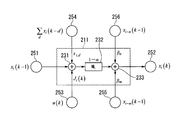
- FIG. 2 is a diagram showing an example of the arithmetic unit block 211 according to the embodiment of the present invention.
- the calculation unit block 211 includes an addition unit 231, a non-linear calculation unit 232, and an addition unit 233. Further, FIG. 2 shows five input terminals 251 and 253 to 256 to the operation unit block 211 and one output end 252 from the operation unit block 211. In this embodiment, these input ends 251 and 253 to 256 and output ends 252 are virtual terminals for convenience of explanation. Note that these input ends 251 and 253 to 256 and output ends 252 may actually be provided in, for example, the arithmetic unit block 211.
- the number of stages in which operations are performed in parallel in space in the reservoir is L.
- L represents an integer of 2 or more.
- i represents an integer of 1 or more and L or less as a variable.
- k represents a value corresponding to time.
- k represents a discrete timing and represents an integer.
- k may not represent the actual time, that is, when operations are performed in parallel in time in the reservoir, it does not necessarily represent the actual time. That is, the unit of time may be an arbitrary unit.
- a signal x i (k-1) is input to the input terminal 251.
- the arithmetic unit block 211 shown in FIG. 2 is the i-th stage block.
- the signal x i (k-1) represents a signal output from the arithmetic unit block 211 as a time (k-1) signal. That is, in the example of FIG. 2, the signal output from the calculation unit block 211 is input to the calculation unit block 211 again.
- a signal x i (k) is output from the output end 252.
- the signal x i (k-1) represents a signal output from the arithmetic unit block 211 as a time (k-1) signal.
- the signal x i (k) represents a signal output from the operation unit block 211 as a time (k) signal.
- a signal u (k) is input to the input end 253.
- the signal u (k) represents a signal input to the reservoir as a time (k) signal.
- a signal ⁇ x i (kd) is input to the input end 254.
- ⁇ represents the sum of two or more predetermined d's.
- d represents an integer. That is, the signal ⁇ x i (kd) represents the sum of the signals of two or more different timings output from the operation unit block 211.
- the input terminal 255, the signal x i-m (k-1 ) is input.
- Signal x i-m (k-1 ) is, as a signal in the time (k-1), represents the signal output from the (i-m) th stage operation unit blocks.
- m represents an integer, and in the present embodiment, represents an integer of 1 or more and (i-1) or less.
- one input terminal 255 is shown. For example, among m being 1 or more and (i-1) or less, two or more input terminals are provided in parallel. May be good. In the example of FIG. 2, only one input end 255 is shown for simplification of illustration.
- a signal x i + n (k-1) is input to the input terminal 256.
- the signal x i + n (k-1) represents a signal output from the arithmetic unit block of the (i + n) stage as a time (k-1) signal.
- n represents an integer, and in the present embodiment, represents an integer of 1 or more and (Li) or less.
- one input terminal 256 is shown. For example, among those in which n is 1 or more and (Li) or less, two or more input terminals are provided in parallel. May be good. In the example of FIG. 2, only one input end 256 is shown for simplification of illustration.
- the signal is inputted from the input terminal 251 x i (k-1) is input to the adder 231.
- the signal is inputted from the input terminal 253 u (k) is converted into a signal J i (k) is input to the adder 231.
- the signal J i (k) is represented by the formula (2). That is, the signal J i (k) is the signal u (k), the result of a predetermined coefficient w in, i have been multiplied.
- the predetermined coefficients win and i may be arbitrary values or may be 0. In the example of FIG. 2, the illustration is simplified, and the multiplication unit for multiplying the predetermined coefficients win and i is omitted from the illustration.
- the signal ⁇ x i (kd) input from the input end 254 is multiplied by the predetermined coefficients s i and d , and then the multiplication result is input to the addition unit 231.
- the predetermined coefficients s i and d may be arbitrary values or may be 0. In the example of FIG. 2, the illustration is simplified, and the multiplication portion for multiplying the predetermined coefficients si and d is omitted from the illustration.
- signal x is inputted from-i m (k-1) , a predetermined coefficient beta m are multiplied, the multiplication result is inputted to the adder 233.
- the multiplication result is input to the addition unit 233 for one or more types of m.
- the illustration is simplified, and the multiplication portion for multiplying the predetermined coefficient ⁇ m is omitted.
- the signal x i + n (k-1) input from the input end 256 is multiplied by a predetermined coefficient ⁇ n , and the multiplication result is input to the addition unit 233.
- the multiplication result is input to the addition unit 233 for one or more types of n.
- the illustration is simplified, and the multiplication part for multiplying the predetermined coefficient ⁇ n is omitted.
- the addition unit 231 adds the input signals x i (k-1), signal J i (k), and signal s i, d ⁇ x i (kd), and adds the addition result to the non-linear calculation unit. Output to 232.
- the nonlinear calculation unit 232 substitutes the signal input from the addition unit 231 into z of the predetermined nonlinear function F NL (z).
- F NL (z) represents a non-linear function with z as a variable.
- the nonlinear function is not particularly limited, and for example, a sigmoid function or a hyperbolic tangent function may be used.
- the nonlinear calculation unit 232 outputs the calculation result of the nonlinear function F NL (z).
- the output calculation result is multiplied by a predetermined coefficient (1- ⁇ ) and input to the addition unit 233.
- ⁇ may be any value.
- the illustration is simplified, and the multiplication portion for multiplying the predetermined coefficient (1- ⁇ ) is omitted.
- the addition unit 233 is a signal (1- ⁇ ) F NL (z) which is an input signal, a sum of the signals ⁇ m x im (k-1) with respect to m, and a signal ⁇ n x i + n (k-1). The sum of n is added, and the addition result is output to the output terminal 252. That is, the addition result is represented by the equation (1).
- m and n may be arbitrary integers, for example, positive values, negative values, or zero. You may.
- the side of the input end 255 and the side of the input end 256 may have substantially the same configuration.
- the input signal x im (k-1) from the input terminal 255 and the input signal x i + n (k-1) from the input terminal 256 may have different configurations.
- the m and the n are the same value, when m and n a positive value, as spatially symmetric two input signals, the input signal x i-m (k-1 ) and the input signal x i + n (k-1) is input to the addition unit 233.
- a configuration may be used in which the input ends to the addition unit 233 are only two input ends 255 and 256.
- the addition unit 231, the non-linear calculation unit 232, and the addition unit 233 may be configured by using arbitrary circuits, respectively.
- the coefficients s i, d , the coefficients win , i , the coefficient (1- ⁇ ), the coefficients ⁇ m , and ⁇ n which are weights for the signal, may be arbitrary values, for example, 1. It may be present, or it may be 0.
- the coefficient that is the weight for the signal is 1, the signal is not changed.
- the coefficient that becomes the weight for the signal it corresponds to the configuration in which the signal is not used at the place of the weight.
- a configuration in which the coefficient serving as a weight is multiplied may be used as another configuration example.
- FIG. 3 is a diagram showing an example of the arithmetic unit block 311 according to the embodiment of the present invention.
- the same components as those shown in FIG. 2 are designated by the same reference numerals, and detailed description thereof will be omitted.
- the calculation unit block 311 includes an addition unit 231, a non-linear calculation unit 232, and an addition unit 233. Further, FIG. 3 shows four input terminals 251 and 253 to 255 to the operation unit block 311 and one output end 252 from the operation unit block 311.
- the arithmetic unit block 311 is different from the arithmetic unit block 211 shown in FIG. 2 in that a system from the input end 256 to the addition unit 233 is not provided, and is the same in other respects.
- the signal output from the arithmetic unit block 311 to the output terminal 252 is represented by the equation (3). That is, in the signal, there is no term corresponding to the system.
- m may be an arbitrary integer, for example, a positive value, a negative value, or zero.
- the arithmetic unit block 311 shown in FIG. 3 may have substantially the same configuration as the arithmetic unit block 211 shown in FIG.
- a configuration may be used in which the input end to the addition unit 233 is only one input end 255.
- FIG. 4 is a diagram showing an example of the arithmetic unit block 411 according to the embodiment of the present invention.
- the same components as those shown in FIG. 2 are designated by the same reference numerals, and detailed description thereof will be omitted.
- the calculation unit block 411 includes an addition unit 231, a non-linear calculation unit 232, and an addition unit 233. Further, FIG. 4 shows four input terminals 251, 253, 255 to 256 to the operation unit block 411 and one output end 252 from the operation unit block 411.
- the arithmetic unit block 411 is different from the arithmetic unit block 211 shown in FIG. 2 in that a system from the input end 254 to the addition unit 231 is not provided, and is the same in other respects.
- the signal output from the arithmetic unit block 411 to the output terminal 252 is represented by the equation (4). That is, in the signal, there is no term corresponding to the system.
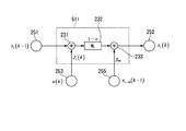
- FIG. 5 is a diagram showing an example of the arithmetic unit block 511 according to the embodiment of the present invention.
- the same components as those shown in FIG. 2 are designated by the same reference numerals, and detailed description thereof will be omitted.
- the calculation unit block 511 includes an addition unit 231, a non-linear calculation unit 232, and an addition unit 233. Further, FIG. 5 shows four input terminals 251 and 253, 255 to the operation unit block 511 and one output end 252 from the operation unit block 511.
- the arithmetic unit block 511 is not provided with a system from the input end 254 to the addition unit 231 and a system from the input end 256 to the addition unit 233 as compared with the arithmetic unit block 211 shown in FIG. It differs in, and is similar in other respects.
- the signal output from the arithmetic unit block 511 to the output terminal 252 is represented by the equation (5). That is, in the signal, there is no term corresponding to these systems.
- the input to the addition unit 233 is performed.
- the configuration can be substantially the same as that of the arithmetic unit block 411 shown in FIG.
- any arithmetic unit block among the arithmetic unit blocks 211, 311, 411, and 511 shown in FIGS. 2 to 5 is configured (or reconstructed). It may have a plurality of arithmetic unit blocks capable of performing.
- an arithmetic unit block for example, an arithmetic unit block that can be configured as the arithmetic unit block 211 shown in FIG. 2 may be used. That is, the arithmetic unit block that can be configured as the arithmetic unit block 211 shown in FIG. 2 is configured as the arithmetic unit blocks 311, 411, and 511 shown in FIGS. 3 to 5 by omitting the connection of some wirings. obtain.
- the array unit 21 may have an arbitrary operation unit block as each of the plurality of operation unit blocks.
- FIGS. 6 to 11 A configuration example of the array unit 21 is shown with reference to FIGS. 6 to 11.
- the configurations shown in FIGS. 6 to 11 may be used, for example, as the entire configuration of the array unit 21, or may be used as a partial configuration of the array unit 21.
- the arithmetic unit block arranged at the end such as the first stage spatially or temporally
- another arithmetic unit block is used.
- the input source may be different for the operation unit block of the stage.
- the operation unit block arranged at the end such as the first stage is applicable.
- Other stages may not exist, in which case an input end or the like for inputting an alternative signal may be provided.
- the input signal from the input layer 41 may be given with weight to the input end.
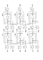
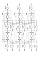
- FIG. 6 is a diagram showing a configuration example of the array unit 21 according to the embodiment of the present invention.
- three stages of arithmetic unit blocks 611 to 613 are provided in parallel in space.
- the calculation unit block 611 in the (i-1) stage, the calculation unit block 612 in the i-th stage, and the calculation unit block 613 in the (i + 1) stage are shown.
- Each of the three-stage arithmetic unit blocks 611 to 613 is an arithmetic unit block that performs the same arithmetic as the arithmetic unit block 511 shown in FIG.
- the input ends 631, 651, and 671 correspond to the input ends 251 shown in FIG. 5, and the input ends 633, 653, and 673 correspond to the input ends 253 shown in FIG.
- the output ends 632, 652, and 672 correspond to the output ends 252 shown in FIG. It is assumed that all these input ends 631, 651, 671 and input ends 633, 653, 673 and output ends 632, 652, 672 are connected to the wirings of CB 111 to 116 and IB 121 to 128 shown in FIG. ..
- the input end 671 of the operation unit block 613 of the next stage (i + 1) is used as the input end 255 shown in FIG. That is, the input end 671 of the arithmetic unit block 613 in the (i + 1) th stage is shared by the input to the arithmetic unit block 613 and the input to the arithmetic unit block 612 in the previous stage.
- the efficiency of the spatial configuration in the present embodiment, the efficiency of the configuration in the direction of the number of stages
- the configuration for three stages in parallel in space (calculation unit blocks 611 to 613) is shown, but for example, the configuration for two stages in parallel in space may be used. Alternatively, a configuration of four or more stages may be used in parallel in space.
- the configuration in which the input end of the arithmetic unit block of a certain stage is used for input to the arithmetic unit block of the previous stage is shown, but as another example, the input end of the arithmetic unit block of a certain stage is used.
- the configuration used for input to the operation unit block in the subsequent stage may be used.
- FIG. 7 is a diagram showing a configuration example of the array unit 21 according to the embodiment of the present invention.
- the same components as those shown in FIG. 6 are designated by the same reference numerals.
- the three arithmetic unit blocks 611 to 613, the input ends 631, 651, 671, the input ends 633, 653, 673, and the output ends 632, 652, 672 are as shown in FIG. The same is true. It is assumed that all these input ends 631, 651, 671 and input ends 633, 653, 673 and output ends 632, 652, 672 are connected to the wirings of CB 111 to 116 and IB 121 to 128 shown in FIG. ..
- each of the three-stage arithmetic unit blocks 711 to 713 is an arithmetic unit block that performs the same arithmetic as the arithmetic unit block 511 shown in FIG.
- the input ends 732, 752, and 772 correspond to the input ends 253 shown in FIG. 5, and the output ends 731, 751, and 771 correspond to the output ends 252 shown in FIG. It is assumed that all these input ends 732, 752, 772 and output ends 731, 751, 771 are connected to the wirings of CB 111 to 116 and IB 121 to 128 shown in FIG.
- each of the calculation unit blocks 711 to 713 as input ends corresponding to the input ends 251 shown in FIG. 5, the output ends 632, 652, and 672 of the respective calculation unit blocks 611 to 613 in the previous stage in time are used. It is shared. As a result, the efficiency of the configuration in time (in the present embodiment, the efficiency of the configuration in the direction of time) is achieved.
- FIG. 8 is a diagram showing a configuration example of the array unit 21 according to the embodiment of the present invention.
- the same components as those shown in FIG. 7 are designated by the same reference numerals.
- the three arithmetic unit blocks 611 to 613, the input ends 631, 651, 671, the input ends 633, 653, 673, and the output ends 632, 652, 672 are as shown in FIG. The same is true.
- the three arithmetic unit blocks 711 to 713, the input terminals 732, 752, 772, and the output terminals 731, 751, 771 are the same as those shown in FIG.
- each of the three-stage arithmetic unit blocks 811 to 813 is an arithmetic unit block that performs the same arithmetic as the arithmetic unit block 511 shown in FIG.
- the input ends 832, 852, and 872 correspond to the input ends 253 shown in FIG. 5, and the output ends 831, 851, 871 correspond to the output ends 252 shown in FIG. It is assumed that all the input terminals 832, 852, 872 and the output terminals 831, 851, 871 are connected to the wirings of CB 111 to 116 and IB 121 to 128 shown in FIG.
- each of the calculation unit blocks 811 to 813 as input ends corresponding to the input ends 251 shown in FIG. 5, the output ends 731, 751, 771 of the respective calculation unit blocks 711 to 713 in the previous stage in time are used. It is shared. As a result, the efficiency of the temporal configuration (in the present embodiment, the efficiency of data flow control in the time direction) is achieved.
- the configuration in which the calculation unit blocks are provided in parallel in the 1st to 3rd stages in time is shown, but as another example, the calculation is performed in parallel in 4 or more stages in time.
- a configuration including a unit block may be used.
- FIG. 9 is a diagram showing a configuration example of the array unit 21 according to the embodiment of the present invention.
- three stages of arithmetic unit blocks 911 to 913 are provided in parallel in space.
- the calculation unit block 911 in the (i-1) stage, the calculation unit block 912 in the i-th stage, and the calculation unit block 913 in the (i + 1) stage are shown.
- Each of the three-stage arithmetic unit blocks 911 to 913 is an arithmetic unit block that performs the same arithmetic as the arithmetic unit block 411 shown in FIG.
- the input ends 931, 951 and 971 correspond to the input ends 251 shown in FIG. 4, and the input ends 933, 953 and 973 correspond to the input ends 253 shown in FIG.
- the output ends 932, 952, 972 correspond to the output ends 252 shown in FIG. It is assumed that all these input ends 931, 951, 971 and input ends 933, 953, 973 and output ends 932, 952, 972 are connected to the wirings of CB 111 to 116 and IB 121 to 128 shown in FIG. ..
- the input end 971 of the operation unit block 913 of the next stage (i + 1) is used as the input end 255 shown in FIG. That is, the input end 971 of the arithmetic unit block 913 in the (i + 1) th stage is shared by the input to the arithmetic unit block 913 and the input to the arithmetic unit block 912 in the previous stage.
- the efficiency of the spatial configuration in the present embodiment, the efficiency of data flow control in the direction of the number of stages
- the input end 931 of the operation unit block 911 of the previous stage (i-1) is used as the input end 256 shown in FIG. That is, the input end 931 of the operation unit block 911 in the (i-1) stage is shared by the input to the operation unit block 911 and the input to the operation unit block 912 in the next stage.
- the efficiency of the spatial configuration in the present embodiment, the efficiency of data flow control in the direction of the number of stages
- the input end 951 of the operation unit block 912 in the i-th stage has an input to the operation unit block 912, an input to the operation unit block 911 in the previous stage (i-1), and the next. It is used for input to the arithmetic unit block 913 of the (i + 1) th stage, which is the stage.
- the configuration for three stages in parallel in space (calculation unit blocks 911 to 913) is shown, but for example, the configuration for two stages in parallel in space may be used. Alternatively, a configuration of four or more stages may be used in parallel in space.
- Each of the three-stage arithmetic unit blocks 1011 to 1013 is an arithmetic unit block that performs the same arithmetic as the arithmetic unit block 411 shown in FIG.
- the input ends 1032, 1052, and 1072 correspond to the input ends 253 shown in FIG. 4, and the output ends 1031, 1051, and 1071 correspond to the output ends 252 shown in FIG. It is assumed that all these input ends 1032, 1052, 1072 and output ends 1031, 1051, 1071 are connected to the wirings of CB 111 to 116 and IB 121 to 128 shown in FIG.
- each of the calculation unit blocks 1011 to 1013 as input ends corresponding to the input ends 251 shown in FIG. 4, the output ends 932, 952, 972 of the respective calculation unit blocks 911 to 913 in the previous stage in time are used. It is shared. As a result, the efficiency of the temporal configuration (in the present embodiment, the efficiency of data flow control in the time direction) is achieved.
- FIG. 10 is a diagram showing a configuration example of the array unit 21 according to the embodiment of the present invention.
- the same components as those shown in FIG. 9 are designated by the same reference numerals.
- the three arithmetic unit blocks 911 to 913, the input ends 931, 951, 971, the input ends 933, 953, 973, and the output ends 932, 952, 972 are as shown in FIG. The same is true.
- the three arithmetic unit blocks 1011 to 1013, the input terminals 1032, 1052, 1072, and the output ends 1031, 1051, 1071 are the same as those shown in FIG. It is assumed that all these input ends 1032, 1052, 1072 and output ends 1031, 1051, 1071 are connected to the wirings of CB 111 to 116 and IB 121 to 128 shown in FIG.
- each of the three-stage arithmetic unit blocks 1111 to 1113 is an arithmetic unit block that performs the same arithmetic as the arithmetic unit block 411 shown in FIG.
- the input ends 1132, 1152, and 1172 correspond to the input ends 253 shown in FIG. 4, and the output ends 1131, 1151, and 1171 correspond to the output ends 252 shown in FIG. It is assumed that all the input terminals 1132, 1152, 1172 and the output terminals 1131, 1151, 1171 are connected to the wirings of CB 111 to 116 and IB 121 to 128 shown in FIG.
- each of the calculation unit blocks 1111 to 1113 as input ends corresponding to the input ends 251 shown in FIG. 4, the output ends 1031, 1051, and 1071 of the respective calculation unit blocks 1011 to 1013 in the previous stage in terms of time are used. It is shared. As a result, the efficiency of the temporal configuration (in the present embodiment, the efficiency of data flow control in the time direction) is achieved.
- the configuration in which the arithmetic unit blocks are provided in parallel in the 2nd to 3rd stages in time is shown, but as another example, the arithmetic unit blocks are provided in 1 stage in time.
- a configuration provided or a configuration in which arithmetic unit blocks are provided in parallel in four or more stages in terms of time may be used.
- FIG. 11 is a diagram showing a configuration example of the array unit 21 according to the embodiment of the present invention.
- three stages of arithmetic unit blocks 1211 to 1213 are provided in parallel in space.
- the calculation unit block 1211 in the (i-1) stage, the calculation unit block 1212 in the i-th stage, and the calculation unit block 1213 in the (i + 1) stage are shown.
- Each of the three-stage arithmetic unit blocks 1211 to 1213 is an arithmetic unit block that performs the same arithmetic as the arithmetic unit block 211 shown in FIG.
- the input ends 1231, 1251 and 1271 correspond to the input ends 251 shown in FIG. 2, and the input ends 1233, 1253 and 1273 correspond to the input ends 253 shown in FIG.
- the output ends 1232, 1252, 1272 correspond to the output ends 252 shown in FIG. It is assumed that all these input ends 1231, 1251, 1271, input ends 1233, 1253, 1273 and output ends 1232, 1252, 1272 are connected to the wirings of CB 111 to 116 and IB 121 to 128 shown in FIG. ..
- the input end 1271 of the operation unit block 1213 of the next stage (i + 1) is used as the input end 255 shown in FIG. That is, the input end 1271 of the arithmetic unit block 1213 in the (i + 1) th stage is shared by the input to the arithmetic unit block 1213 and the input to the arithmetic unit block 1212 in the previous stage.
- the efficiency of the spatial configuration in the present embodiment, the efficiency of data flow control in the direction of the number of stages
- the input end 1231 of the operation unit block 1211 of the previous stage (i-1) is used as the input end 256 shown in FIG. That is, the input end 1231 of the operation unit block 1211 in the (i-1) stage is shared by the input to the operation unit block 1211 and the input to the operation unit block 1212 in the next stage.
- the efficiency of the spatial configuration in the present embodiment, the efficiency of data flow control in the direction of the number of stages
- the input end 1251 of the operation unit block 1212 in the i-th stage has an input to the operation unit block 1212, an input to the operation unit block 1211 in the previous stage (i-1), and the next. It is used for input to the arithmetic unit block 1213 of the (i + 1) th stage, which is the stage.
- the configuration for three stages in parallel in space (calculation unit blocks 1211-1213) is shown, but for example, the configuration for two stages in parallel in space may be used. Alternatively, a configuration of four or more stages may be used in parallel in space.
- each of the three-stage arithmetic unit blocks 1311 to 1313 is an arithmetic unit block that performs the same arithmetic as the arithmetic unit block 211 shown in FIG.
- the input ends 1332, 1352, and 1372 correspond to the input ends 253 shown in FIG. 2, and the output ends 1331, 1351, 1371 correspond to the output ends 252 shown in FIG. It is assumed that all these input ends 1332, 1352, 1372 and output ends 1331, 1351, 1371 are connected to the wirings of CB 111 to 116 and IB 121 to 128 shown in FIG.
- each of the calculation unit blocks 1311-1313 as input ends corresponding to the input ends 251 shown in FIG. 2, the output ends 1232, 1252, 1272 of the respective calculation unit blocks 1211-1213 in the previous stage in terms of time are used. It is shared. As a result, the efficiency of the temporal configuration (in the present embodiment, the efficiency of data flow control in the time direction) is achieved.
- each of the calculation unit blocks 1311-1313 as input ends corresponding to the input ends 254 shown in FIG. 2, the input ends 1231, 1251, 1271 of the respective calculation unit blocks 1211 to 1213 in the previous stage in terms of time are used. It is shared. As a result, the efficiency of the temporal configuration (in the present embodiment, the efficiency of data flow control in the time direction) is achieved.
- the input end 1251 of the operation unit block 1212 in the i-th stage is used for the input to the operation unit block 1212 and the input to the operation unit block 1312 in the next stage in terms of time.
- the configuration in which the arithmetic unit blocks are provided in parallel in two stages in time is shown, but as another example, the configuration in which the arithmetic unit blocks are provided in one stage in time, or A configuration in which arithmetic unit blocks are provided in parallel in three or more stages in terms of time may be used.
- the reservoir calculation data flow processor 1 provides a reconfigurable machine learning device for physically implementing a reservoir calculation function having a time-series signal generation, prediction, identification, or detection function.
- the reservoir calculation data flow processor 1 according to the present embodiment includes, as the machine learning device, a calculation unit block which is a minimum constituent unit of a reservoir that performs a predetermined calculation and generates and holds (buffers) time series information.
- the calculation unit block is the smallest unit reservoir unit constituting the reservoir. Therefore, the reservoir calculation data flow processor 1 according to the present embodiment can provide, for example, hardware that executes reservoir calculation for a time series signal in real time.
- the power consumption is small and the overall processing time is long.
- the power consumption is large and the overall processing time is short. For example, by adjusting these trade-offs, it is possible to improve the performance of the device.
- the reservoir calculation data flow processor 1 can provide, for example, a dedicated device for streamlining the data flow and optimizing the throughput for implementing the reservoir calculation function.
- the reservoir calculation data flow processor 1 according to the present embodiment for example, by deriving a mathematically equivalent data flow graph at the time of design, it is possible to realize a reservoir of an arbitrary scale and various network configurations.
- the reservoir calculation data flow processor 1 for example, it is possible to flexibly cope with the expansion of the operation equation of the mathematical model to be implemented.
- the embodiments of FIGS. 7 to 8 correspond to the mathematical model proposed in Non-Patent Document 1
- the embodiments of FIGS. 9 to 10 correspond to 1 of the mathematical model proposed in Non-Patent Document 2.
- the embodiment of FIG. 11 corresponds to one of the mathematical models proposed in Non-Patent Document 3.
- an in-memory computing architecture In-Memory Computing Architecture
- NVM Non-Volatile Memory
- it can be realized as an optical waveguide device by implementing a nonlinear calculation function by an optical modulator and a data flow graph on an optical waveguide.
- the parameters and the network configuration can be changed in a programmable manner. Therefore, in the reservoir calculation data flow processor 1 according to the present embodiment, by making it possible to change the parameters and the network configuration programmable as a module configuration, for example, a designer (an example of a user) can easily specify a specific application. Reservoir configuration can be modified to achieve a customized physical implementation. For example, in the reservoir calculation data flow processor 1 according to the present embodiment, when the reservoir is mounted, it is mathematically associated with the reservoir having a one-dimensional ring topology configuration, thereby providing a theoretical and systematic concrete architecture. The parameters can be determined.
- the reservoir calculation data flow processor 1 takes in a signal resulting from multiplying the input signal (in the present embodiment, the signal u (k)) by a weight, and holds the signal and the signal one hour before. Alternatively, by adding the state values before that, the first intermediate signal (in the present embodiment, the signal input to the nonlinear calculation unit 232) is generated. Further, the reservoir calculation data flow processor 1 according to the present embodiment generates a second intermediate signal (in the present embodiment, a signal output from the nonlinear calculation unit 232) by performing a nonlinear conversion on the first intermediate signal.
- the reservoir calculation data flow processor 1 for example, a signal from an adjacent module is received, an interaction term obtained by multiplying the signal by a weight is calculated, and the interaction term and the second intermediate signal are calculated. by adding the bets, (in the present embodiment, the signal x i (k)) output signal as a state value of the next time to generate. Therefore, in the reservoir calculation data flow processor 1 according to the present embodiment, the minimum structural unit of the reservoir that generates and holds the time series information can be concretely realized in the reservoir calculation.
- the reservoir calculation data flow processor 1 In the reservoir calculation data flow processor 1 according to the present embodiment, it is represented by a data flow graph using the minimum structural unit. Therefore, in the reservoir calculation data flow processor 1 according to the present embodiment, it is easy to design a structural unit for mounting a reservoir layer using a wide variety of devices (for example, digital hardware devices) such as FPGA or ASIC. can do. For example, in the reservoir calculation data flow processor 1 according to the present embodiment, when it is implemented in FPGA, ASIC, or the like, it is possible to realize efficient computing resources and hardware for efficient data flow control. It will be possible.
- the reservoir calculation data flow processor 1 by combining a plurality of machine learning devices, it is possible to realize a network configuration having an arbitrary scale and various two-dimensional topologies. Further, in the reservoir calculation data flow processor 1 according to the present embodiment, the reservoir having such a network configuration can be graphically represented by a data flow representation. Therefore, in the present embodiment, the device operation can be systematically analyzed and reflected in the design based on the data flow representation.
- the reservoir calculation data flow processor 1 In the reservoir calculation data flow processor 1 according to the present embodiment, machine learning devices can be integrated and implemented, and for example, a network configuration corresponding to an extended model of reservoir calculation can be realized. Therefore, in the reservoir calculation data flow processor 1 according to the present embodiment, for example, the reservoir layer can be implemented in FPGA, ASIC, or the like based on different expansion models.
- a data flow graph that converts sequential operations executed by virtual nodes in a time-divided manner into parallel and distributed operations by spatially arranged physical nodes is theoretically derived, and as its physical implementation.
- Reservoir calculation data flow processor 1 can be provided.
- the reservoir configuration coupling structure
- problems scaling and scalability due to the complexity of wiring can be achieved. Problems such as variation in wiring delay) can be solved.
- the reservoir calculation data flow processor includes a plurality of reservoir units (DRU in the example of FIG. 1) that are units constituting the reservoir. By changing the connection relationship between the reservoir units, the reservoir can be reconfigured by a plurality of reservoir units.
- the reservoir unit includes a calculation unit block (in the example of FIG. 1, a DRU calculation circuit) that executes a predetermined calculation.
- the arithmetic unit block is the result of multiplying the output from the first addition unit or the output by a predetermined coefficient with the first addition unit (addition unit 231 in the examples of FIGS. 2 to 5) that adds at least two inputs. (In the example of FIGS.
- non-linear calculation unit 232 in the examples of FIGS. 2 to 5
- the output from the non-linear calculation unit or the said is included.
- a second addition unit that adds at least two inputs including the result of multiplying the output by a predetermined coefficient (in the example of FIGS. 2 to 5, the result of multiplying the predetermined coefficient) (addition in FIGS. 2 to 5). Part 233) is included.
- the calculation unit block further includes a block for connecting the reservoir units (CB111 to 116 in the example of FIG. 1) and a block for input / output (FIG. 1).
- IB121-128 is included in the example of 1, IB121-128) is included.
- the reservoir calculation data flow processor further includes a data flow control unit (data flow control unit 22 in the example of FIG. 1) that switches the connection relationship between the reservoir units.
- a user-configured reservoir in a reservoir calculation data flow processor, can be reconfigured (ie, programmable).
- the reservoir in the reservoir calculation data flow processor, the reservoir can be reconfigured based on predetermined information (in the example of FIG. 1, the data flow control unit 22 reconfigures the reservoir).
- a plurality of arithmetic unit blocks are spatially arranged in parallel. Thereby, for example, it is possible to process a plurality of signals at the same time in parallel.
- a plurality of arithmetic unit blocks are arranged in parallel in time. Thereby, for example, it is possible to process a plurality of signals at different times in the same spatial stage in parallel.
- the first adder is at least a signal corresponding to an output signal from the second adder before (that is, a time corresponding to the past) in time or the signal.
- the result of multiplying the predetermined coefficient and the input signal to the reservoir or the result of multiplying the input signal by the predetermined coefficient are added (for example, the examples of FIGS. 2 to 5).
- the second addition unit has at least the output from the non-linear arithmetic unit or the result of multiplying the output by a predetermined coefficient, and a plurality of stages arranged in parallel spatially. The signal corresponding to the output signal from the second addition unit of the other stage (that is, the other stage) or the result of multiplying the signal by a predetermined coefficient is added.
- a program for realizing the function of an arbitrary component in an arbitrary device such as the reservoir calculation data flow processor described above is recorded on a computer-readable recording medium, and the program is read into the computer system. You may want to do it.
- the term "computer system” as used herein includes hardware such as an operating system (OS: Operating System) or peripheral devices.
- the "computer-readable recording medium” refers to a portable medium such as a flexible disk, a magneto-optical disk, a ROM, a CD (Compact Disc) -ROM, or a storage device such as a hard disk built in a computer system. ..
- a "computer-readable recording medium” is a constant, such as the volatile memory inside a computer system that serves as a server or client when a program is transmitted via a network such as the Internet or a communication line such as a telephone line. It shall include those holding a time program.
- the volatile memory may be, for example, RAM.
- the recording medium may be, for example, a non-temporary recording medium.
- the above program may be transmitted from a computer system in which this program is stored in a storage device or the like to another computer system via a transmission medium or by a transmission wave in the transmission medium.
- the "transmission medium" for transmitting a program refers to a medium having a function of transmitting information, such as a network such as the Internet or a communication line such as a telephone line.
- the above program may be for realizing a part of the above-mentioned functions.
- the above program may be a so-called difference file that can realize the above-mentioned functions in combination with a program already recorded in the computer system.
- the difference file may be called a difference program.
- each process in the present embodiment may be realized by a microprocessor that operates based on information such as a program and a computer-readable recording medium that stores information such as a program.
- the functions of each part may be realized by individual hardware, or the functions of each part may be realized by integrated hardware.
- a microprocessor includes hardware, which may include at least one of a circuit that processes a digital signal and a circuit that processes an analog signal.
- a microprocessor may be configured using one or more circuit devices mounted on a circuit board, or one or both of one or more circuit elements.
- An IC (Integrated Circuit) or the like may be used as the circuit device, and a resistor or a capacitor may be used as the circuit element.
- the reservoir calculation data flow processor is based on, for example, a CPU, a GPU (Graphics Processing Unit), or a DSP (Digital Signal) based on the data flow representation of the mathematical model of the reservoir shown in the embodiment of the present invention. It may be implemented on various digital processors such as Processor) and the like. Further, the reservoir calculation data flow processor may be, for example, a hardware circuit by FPGA. Further, the reservoir calculation data flow processor may be composed of, for example, a plurality of CPUs, a plurality of FPGAs, or a hardware circuit by a plurality of ASICs. Good.
- the reservoir calculation data flow processor may be composed of, for example, a combination of a plurality of CPUs and a plurality of hardware circuits by ASICs. Further, the reservoir calculation data flow processor may include, for example, one or more of an amplifier circuit or a filter circuit for processing an analog signal.
- the reservoir calculation data flow processor of the present invention it is possible to provide a dedicated reservoir calculation device suitable for configuring a reservoir.
- Non-linear calculation unit 251, 253 to 256, 631, 633, 651, 653, 671, 673, 732, 752, 772, 832, 852, 872, 931, 933, 951, 953, 971, 973, 1032, 1052, 1072, 1132, 1152, 1172, 1231, 1233, 1251, 1253, 1271, 1273, 1332, 1352, 1372 ...
- Input terminal 252, 632 , 652, 672, 731, 751, 771, 831, 851, 871, 932, 952, 972, 1031, 1051, 1071, 1131, 1151, 1171, 1232, 1252, 1272, 1331, 1351, 1371 ...
- Output end 252, 632 , 652, 672, 731, 751, 771, 831, 851, 871, 932, 952, 972, 1031, 1051, 1071, 1131, 1151, 1171, 1232, 1252, 1272, 1331
Landscapes
- Engineering & Computer Science (AREA)
- Physics & Mathematics (AREA)
- Theoretical Computer Science (AREA)
- Computer Hardware Design (AREA)
- General Physics & Mathematics (AREA)
- General Engineering & Computer Science (AREA)
- Life Sciences & Earth Sciences (AREA)
- Evolutionary Computation (AREA)
- Biophysics (AREA)
- Biomedical Technology (AREA)
- Software Systems (AREA)
- Health & Medical Sciences (AREA)
- Computing Systems (AREA)
- Computational Linguistics (AREA)
- Mathematical Physics (AREA)
- General Health & Medical Sciences (AREA)
- Data Mining & Analysis (AREA)
- Molecular Biology (AREA)
- Artificial Intelligence (AREA)
- Geology (AREA)
- Mining & Mineral Resources (AREA)
- Geometry (AREA)
- Fluid Mechanics (AREA)
- General Life Sciences & Earth Sciences (AREA)
- Geochemistry & Mineralogy (AREA)
- Environmental & Geological Engineering (AREA)
- Neurology (AREA)
- Multi Processors (AREA)
- Complex Calculations (AREA)
- Design And Manufacture Of Integrated Circuits (AREA)
Abstract
リザーバを構成する単位となる複数のリザーバユニットを備え、前記リザーバユニット同士の接続関係を変更することにより前記リザーバを再構成可能であり、前記リザーバユニットは、所定の演算を実行する演算単位ブロックを含み、前記演算単位ブロックは、少なくとも2入力の加算を行う第1加算部と、前記第1加算部からの出力または当該出力に所定係数が乗算された結果に非線形関数を施す非線形演算部と、前記非線形演算部からの出力または当該出力に所定係数が乗算された結果を含む少なくとも2入力の加算を行う第2加算部を含む、リザーバ計算データフロープロセッサ。
Description
本発明は、リザーバ計算データフロープロセッサに関する。
時系列信号を扱う機械学習として様々なアルゴリズムとアーキテクチャが提案されている。このような時系列向けの機械学習では、例えば、FPGA(Field Programmable Gate Array)あるいはASIC(Application Specific Integrated Circuit)を用いた集積化実装が進みつつある。
時系列信号は、時々刻々と変化するストリームデータである。時系列信号としては、例えば、工場で稼働する設備およびプロセスの状況を示すセンサデータに相当する信号、あるいは、ウェアラブルデバイスから得られた生体信号などがある。このような時系列信号を計測して分析することにより、機械の故障あるいは生体の疾患の予兆を得ることができる。
時系列信号を扱う機械学習として、過去の出力を現在の入力として再帰的に用いることで時系列信号を扱うことが可能なリカレントニューラルネットワーク(Reccurent Neural Network)があり、その派生であるLSTM(Long Short Term Memory)、あるいは、GRU(Gated Reccurrent Unit)といったアーキテクチャが提案されている。
このようなアーキテクチャでは、時系列信号のサンプリング区間に対応したデータ長のストリームデータに基づいて、ニューラルネットワークの重みパラメータの学習を行うことが必要となる。このため、このようなアーキテクチャでは、エッジデバイスなどに実装してリアルタイムに学習を実行することは難しい場合がある。
機械学習をソフトウェアで、あるいはハードウェアで実装する場合には、いずれの場合においても、学習対象となるニューラルネットワークのアーキテクチャをデータフローグラフにより表現したうえで演算を効率化し、例えば、自動微分によって重みパラメータを効率的に更新することが提案されている。しかし、LSTMやGRUのような再帰型のアーキテクチャにおいては、学習時に実行される順方向伝播と逆方向伝播の計算に資するデータフローグラフを効率的に表現することは難しく、学習の効率化を図るうえでの課題のひとつとなっている。実際に、これまでに提案されている機械学習のためのデータフロープロセッサは、階層型構成のアーキテクチャの深層学習(当該深層学習の畳み込み演算)を対象としたものが中心であり、時系列学習向けのものは殆ど提案されていない。
そこで、リザーバ計算(Reservour Computing) が提案されており、その有効性も示されつつある。
リザーバ計算では、中間層(リザーバ:Reservour)の重みを固定して、出力層(リードアウト:Readout)の部分のみ学習を行うことで学習を軽量化している。つまり、学習時の逆方向伝播に対応する計算を省略化することで、大幅に効率化している。
したがって、このようなリザーバ計算は、例えば、計算資源に制約のあるエッジ学習への応用が期待されている。
しかし、順方向伝播に対応するリザーバの演算(中間層の内部状態値の更新)については、例えば、ハードウェアによる物理実装や、ソフトウェアによる並列計算によって、高速化/効率化を図ることが応用上必要となっている。
リザーバ計算では、中間層(リザーバ:Reservour)の重みを固定して、出力層(リードアウト:Readout)の部分のみ学習を行うことで学習を軽量化している。つまり、学習時の逆方向伝播に対応する計算を省略化することで、大幅に効率化している。
したがって、このようなリザーバ計算は、例えば、計算資源に制約のあるエッジ学習への応用が期待されている。
しかし、順方向伝播に対応するリザーバの演算(中間層の内部状態値の更新)については、例えば、ハードウェアによる物理実装や、ソフトウェアによる並列計算によって、高速化/効率化を図ることが応用上必要となっている。
そこで、これまでにリザーバ計算を高速化/効率化するための様々な技術が提案されている。
例えば、非特許文献1では、理論的な立場から、1次元リングトポロジーのリザーバと特定の重みパラメータ分布を持つ相互結合のリザーバとは数学的に等価であることが示されている(非特許文献1参照。)。
例えば、非特許文献2および非特許文献3では、非特許文献1における理論的解析を拡張した技術が提案されている(非特許文献2-3参照。)。非特許文献2および非特許文献3では、物理実装としては1次元リングトポロジー構成のDelay-time Reservoirによって実装することが想定されている。
このような1次元リングトポロジーのリザーバは、高速に動作する光レーザーでの実装に適したアーキテクチャとなっている。
例えば、非特許文献1では、理論的な立場から、1次元リングトポロジーのリザーバと特定の重みパラメータ分布を持つ相互結合のリザーバとは数学的に等価であることが示されている(非特許文献1参照。)。
例えば、非特許文献2および非特許文献3では、非特許文献1における理論的解析を拡張した技術が提案されている(非特許文献2-3参照。)。非特許文献2および非特許文献3では、物理実装としては1次元リングトポロジー構成のDelay-time Reservoirによって実装することが想定されている。
このような1次元リングトポロジーのリザーバは、高速に動作する光レーザーでの実装に適したアーキテクチャとなっている。
L.Appeltant et al.、"Information processing using a single dynamical node as complex system"、NATURE COMMUNICATIONS、vol.2、Article No.468、13 Sep. 2011
L.Appeltant、"Reservoir computing based on Delay-dynamical Systems"、Vrije Universiteit Brussel May, 2012
J.D.Hart et al.,"Delayed Dynamical Systems:Networks,Chimeras and Reservoir Computing"、[online],、14 Aug,2018,[令和1年10月10日検索]、インターネット<URL:https://arxiv.org/abs/1808.04596>
リザーバ計算に資するリザーバ(中間層)を物理的に実装したハードウェアとして様々なものが提案されているが、これらはいずれもFPGAあるいはASICによるCMOS集積化実装には適しておらず、その設計原理も未だに体系化されていない。
例えば、非特許文献1では、リザーバ(中間層)を物理実装する際に、相互結合構成のアーキテクチャにすることは想定されていない。その代替として、仮想ノードを導入し、時分割による逐次的な非線形演算を施すことで、特定の相互結合構成のリザーバと数学的に等価なリザーバ計算を実現している。
また、非特許文献2-3では、リザーバにおける仮想ノードの動作方程式は導出されているものの、その動作方程式を2次元アレイのFPGAあるいはASICとして集積化実装することについては考えられていない。
また、非特許文献2-3では、リザーバにおける仮想ノードの動作方程式は導出されているものの、その動作方程式を2次元アレイのFPGAあるいはASICとして集積化実装することについては考えられていない。
一般に、数学的に記述された任意のリザーバのモデルをそのまま集積回路上にマッピングすることができるとは限らない。リザーバ計算に資するリザ―バ本体の構成(結合構造)は1次元リングトポロジーや2次元アレイのように隣接結合に限定されたものではない。したがって、リザーバの数学的モデルを物理的に実装するためには、リザーバを構成するノード(ニューロン)を空間的に並列に配置したうえで、複雑なノード間の結線(配線)を実現することが必要になる。
しかしながら、リザーバを集積回路として物理的に実装する際に配線層として利用できる資源には制約がある。例えば、標準的な半導体プロセスでは最大5層のメタル層を配線として利用することができるとしても、ノード間の配線の交差できる数には上限が存在するため、リザーバの規模が大きくなり、ノード数(n)が増加し配線の複雑性(O(n2))が高くなると、現実的に実装することは困難になる。
また、リザーバをハードウェアとして実装した際に、順方向伝播に対応した演算を効率化するようなデータフローが実現されるとは限らない。例えば、リザーバの数学モデルを表現したデータフローグラフが複雑になると、リザーバを構成するノード間の配線長が異なってくるため、それぞれの配線遅延がばらついてしまい、数学モデルとの対応づけが保証されなくなる。このことは設計者によるデバイス設計を困難にする。
また、リザーバをハードウェアとして実装した際に、順方向伝播に対応した演算を効率化するようなデータフローが実現されるとは限らない。例えば、リザーバの数学モデルを表現したデータフローグラフが複雑になると、リザーバを構成するノード間の配線長が異なってくるため、それぞれの配線遅延がばらついてしまい、数学モデルとの対応づけが保証されなくなる。このことは設計者によるデバイス設計を困難にする。
このように、従来では、リザーバ計算について、その物理実装としての専用デバイスの検討が不十分であった。特に、配線の複雑性に起因するスケーラビリティの限界を解決する手段については十分に考慮されていない。また、データフロー制御を効率化する手段についても具体的に実装されていない。
本発明は、このような課題を解決するためになされたものであり、リザーバを構成するために適したリザーバ計算専用デバイスであるリザーバ計算データフロープロセッサを提供することを目的とする。
本発明の一態様は、リザーバを構成する単位となる複数のリザーバユニットを備え、前記リザーバユニット同士の接続関係を変更することにより前記リザーバを再構成可能であり、前記リザーバユニットは、所定の演算を実行する演算単位ブロックを含み、前記演算単位ブロックは、少なくとも2入力の加算を行う第1加算部と、前記第1加算部からの出力または当該出力に所定係数が乗算された結果に非線形関数を施す非線形演算部と、前記非線形演算部からの出力または当該出力に所定係数が乗算された結果を含む少なくとも2入力の加算を行う第2加算部を含む、リザーバ計算データフロープロセッサである。
本発明の一態様は、リザーバ計算データフロープロセッサにおいて、前記演算単位ブロックは、さらに、前記リザーバユニット同士を接続するためのブロックと、入出力を行うためのブロックを含み、当該リザーバ計算データフロープロセッサは、さらに、前記リザーバユニット同士の接続関係を切り替えるデータフロー制御部を備える。
本発明の一態様は、リザーバ計算データフロープロセッサにおいて、ユーザによって設定される前記リザーバを再構成可能である。
本発明の一態様は、リザーバ計算データフロープロセッサにおいて、あらかじめ定められた情報に基づいて、前記リザーバを再構成可能である。
本発明の一態様は、リザーバ計算データフロープロセッサにおいて、前記複数の前記演算単位ブロックが、空間的に並列に配置された。
本発明の一態様は、リザーバ計算データフロープロセッサにおいて、前記複数の前記演算単位ブロックが、時間的に並列に配置された。
本発明の一態様は、リザーバ計算データフロープロセッサにおいて、前記第1加算部は、少なくとも、時間的に前の前記第2加算部からの出力信号に相当する信号または当該信号に所定係数が乗算された結果と、前記リザーバへの入力信号または当該入力信号に所定係数が乗算された結果との加算を行う。
本発明の一態様は、リザーバ計算データフロープロセッサにおいて、前記第2加算部は、少なくとも、前記非線形演算部からの出力または当該出力に所定係数が乗算された結果と、空間的に並列に配置された複数段のうちの他段の前記第2加算部からの出力信号に相当する信号または当該信号に所定係数が乗算された結果の加算を行う。
本発明の一態様によれば、リザーバを構成するために適したリザーバ計算データフロープロセッサを提供することができる。
以下、図面を参照し、本発明の実施形態について説明する。
[リザーバ計算データフロープロセッサ]
図1は、本発明の実施形態に係るリザーバ計算データフロープロセッサ1の概略的な構成を示す図である。
なお、図1には、説明の便宜上、直交座標系であるXY座標系を示してある。
図1は、本発明の実施形態に係るリザーバ計算データフロープロセッサ1の概略的な構成を示す図である。
なお、図1には、説明の便宜上、直交座標系であるXY座標系を示してある。
本実施形態では、リザーバ計算データフロープロセッサ1は、デジタル処理を行うASICである。
リザーバ計算データフロープロセッサ1は、アレイ部21と、制御部の一例であるデータフロー制御部22と、記憶部の一例である共有記憶部23を備える。
なお、リザーバ計算データフロープロセッサ1は、共有記憶部23を備えない構成とされてもよい。
本実施形態では、リザーバ計算データフロープロセッサ1は、リザーバ計算の入力層41と出力層42にそれぞれ接続されている。
なお、リザーバ計算データフロープロセッサ1そのものが入力層41と出力層42を備えている必要はない。
リザーバ計算データフロープロセッサ1は、アレイ部21と、制御部の一例であるデータフロー制御部22と、記憶部の一例である共有記憶部23を備える。
なお、リザーバ計算データフロープロセッサ1は、共有記憶部23を備えない構成とされてもよい。
本実施形態では、リザーバ計算データフロープロセッサ1は、リザーバ計算の入力層41と出力層42にそれぞれ接続されている。
なお、リザーバ計算データフロープロセッサ1そのものが入力層41と出力層42を備えている必要はない。
<アレイ部>
アレイ部21について説明する。
アレイ部21は、ビルディングブロック(機能ブロック)として、複数のデジタルリザーバユニット(DRU:Digital Reservour Unit)がアレイ状に配置されて構成されており、各リザーバユニットは、コネクションブロック(CB:Connecting Block)、および入出力インタフェースブロック(IB:I/O Interface Block)といった機能ブロックに接続されている。
本実施形態では、説明の便宜上、デジタルリザーバユニットをDRUと呼ぶことがあり、コネクションブロックをCBと呼ぶことがあり、入出力インタフェースブロックをIBと呼ぶことがある。
アレイ部21について説明する。
アレイ部21は、ビルディングブロック(機能ブロック)として、複数のデジタルリザーバユニット(DRU:Digital Reservour Unit)がアレイ状に配置されて構成されており、各リザーバユニットは、コネクションブロック(CB:Connecting Block)、および入出力インタフェースブロック(IB:I/O Interface Block)といった機能ブロックに接続されている。
本実施形態では、説明の便宜上、デジタルリザーバユニットをDRUと呼ぶことがあり、コネクションブロックをCBと呼ぶことがあり、入出力インタフェースブロックをIBと呼ぶことがある。
DRUは、リザーバの仮想ノードに対応した演算を物理ノードとして実行するための複数の演算器から構成されている。これら複数の演算器は、非線形演算を行う演算器を含む。
CBは、DRUの状態値を中間信号として受けてそれを周囲の異なるDRUへの入力として橋渡しする機能を持つ。また、CBは、ある時刻の各DRUの状態値を保持するメモリ機能を持つ。
IBは、入力層からの入力信号を各DRUに与えるとともに、所望のDRUの状態値を出力信号として出力層に受け渡す機能を持つ。また、IBはある時刻のあるDRUの状態値を次の時刻の同じDRUへの入力としてフィードバックする機能を持つ。なお、IBはある時刻のあるDRUの状態値を次の時刻に限らず、一定時間の後に、任意のDRUへの入力としてフィードバックしてもよい。
CBは、DRUの状態値を中間信号として受けてそれを周囲の異なるDRUへの入力として橋渡しする機能を持つ。また、CBは、ある時刻の各DRUの状態値を保持するメモリ機能を持つ。
IBは、入力層からの入力信号を各DRUに与えるとともに、所望のDRUの状態値を出力信号として出力層に受け渡す機能を持つ。また、IBはある時刻のあるDRUの状態値を次の時刻の同じDRUへの入力としてフィードバックする機能を持つ。なお、IBはある時刻のあるDRUの状態値を次の時刻に限らず、一定時間の後に、任意のDRUへの入力としてフィードバックしてもよい。
本実施形態では、アレイ部21は、複数のDRUが平面上に配置されている。
本実施形態では、説明の便宜上、当該平面において、互いに直交する2つの方向を縦方向と横方向と呼んで説明する。図1の例では、X軸に平行な方向を横方向と呼び、Y軸に平行な方向を縦方向と呼ぶ。また、図1の例では、X軸の正の方向に向かって横方向のDRUの段数が増加し、Y軸の正の方向に向かって縦方向のDRUの段数が増加するとして、説明する。
また、本実施形態では、複数の機能ブロックは、所定のパターンにしたがって配置されている。
本実施形態では、説明の便宜上、当該平面において、互いに直交する2つの方向を縦方向と横方向と呼んで説明する。図1の例では、X軸に平行な方向を横方向と呼び、Y軸に平行な方向を縦方向と呼ぶ。また、図1の例では、X軸の正の方向に向かって横方向のDRUの段数が増加し、Y軸の正の方向に向かって縦方向のDRUの段数が増加するとして、説明する。
また、本実施形態では、複数の機能ブロックは、所定のパターンにしたがって配置されている。
図1の例では、1個のDRUに符号「51(i,j)」を付してある。本実施形態では、DRU51(i,j)と表記することで、各DRUを区別する。
ここで、i(iは1以上の整数)は、縦方向の段数を表しており、本実施形態では、最大値がLであるとする。本実施形態では、Lは2以上の整数である。図1の例では、Lは7である。
また、j(jは1以上の整数)は、横方向の段数を表しており、本実施形態では、最大値がkであるとする。本実施形態では、kは2以上の整数である。図1の例では、kは5である。
ここで、i(iは1以上の整数)は、縦方向の段数を表しており、本実施形態では、最大値がLであるとする。本実施形態では、Lは2以上の整数である。図1の例では、Lは7である。
また、j(jは1以上の整数)は、横方向の段数を表しており、本実施形態では、最大値がkであるとする。本実施形態では、kは2以上の整数である。図1の例では、kは5である。
また、図1の例では、CB111~CB116と表記することで、各CBを区別する。
また、図1の例では、IB121~IB128と表記することで、各IBを区別する。
また、図1の例では、IB121~IB128と表記することで、各IBを区別する。
CB111~116およびIB121~128といった機能ブロックの配置について説明する。
図1の例に限られず、CB111~116およびIB121~128の配置として、様々な配置が用いられてもよい。
なお、図1の例に限られず、アレイ部21において、他の機能ブロックが用いられてもよい。
図1の例に限られず、CB111~116およびIB121~128の配置として、様々な配置が用いられてもよい。
なお、図1の例に限られず、アレイ部21において、他の機能ブロックが用いられてもよい。
図1の例における各機能ブロックの配置について説明する。
例えば、CB111、CB112、CB113、CB114、CB115、CB116は横方向に6個の機能ブロックの配置となるように並べられている。このときCB111~116の個数は横方向のDRU51(i,j)の段数(k)に対して(k+1)となるように配置される。
また、IB121、IB122、IB123、IB124、IB125、IB126、IB127、IB128は縦方向に8個の機能ブロックの配置となるように並べられている。このときIB121~128の個数は縦方向のDRU51(i,j)の段数(L)に対して(L+1)となるように配置される。
例えば、CB111、CB112、CB113、CB114、CB115、CB116は横方向に6個の機能ブロックの配置となるように並べられている。このときCB111~116の個数は横方向のDRU51(i,j)の段数(k)に対して(k+1)となるように配置される。
また、IB121、IB122、IB123、IB124、IB125、IB126、IB127、IB128は縦方向に8個の機能ブロックの配置となるように並べられている。このときIB121~128の個数は縦方向のDRU51(i,j)の段数(L)に対して(L+1)となるように配置される。
縦方向の複数の段数にわたる各CB111~116は横方向の複数の段数にわたる各IB121~128と交差するように配置される。
配線について説明する。
なお、図1に示されている配線の接続関係は、図示のための概略的な一例である。
図1の例に限られず、DRU51(i,j)、CB111~116およびIB121~128に関して、様々な接続関係が用いられてもよい。
図1の例に限られず、DRU51(i,j)、CB111~116およびIB121~128のそれぞれの機能ブロックにおいて、他の機能ブロックと接続する端子の数は、任意の数であってもよい。
それぞれのCB111~116およびIB121~128に含まれる配線の数は、任意の数であってもよい。
なお、図1に示されている配線の接続関係は、図示のための概略的な一例である。
図1の例に限られず、DRU51(i,j)、CB111~116およびIB121~128に関して、様々な接続関係が用いられてもよい。
図1の例に限られず、DRU51(i,j)、CB111~116およびIB121~128のそれぞれの機能ブロックにおいて、他の機能ブロックと接続する端子の数は、任意の数であってもよい。
それぞれのCB111~116およびIB121~128に含まれる配線の数は、任意の数であってもよい。
図1の例における配線について説明する。
DRU51(i,j)は、隣接するそれぞれのCB111~116とIB121~128に対して、端子を介して接続されている。CB111~116およびIB121~128の内部にはバス方式の配線が備わっており、IB121~128とCB111~116の交点はビアを介して接続することができるようになっている。DRU51(i,j)、CB111~116、IB121~128の各機能ブロックはそれぞれスイッチを持っており、データフロー制御部22からの制御信号によってスイッチングすることで、DRU51(i,j)間の結合と併せて入出力信号の経路を変更することができる。すなわち、本実施形態に係るリザーバ計算データフロープロセッサ1は、再構成可能なデータフロープロセッサとなっている。
DRU51(i,j)は、隣接するそれぞれのCB111~116とIB121~128に対して、端子を介して接続されている。CB111~116およびIB121~128の内部にはバス方式の配線が備わっており、IB121~128とCB111~116の交点はビアを介して接続することができるようになっている。DRU51(i,j)、CB111~116、IB121~128の各機能ブロックはそれぞれスイッチを持っており、データフロー制御部22からの制御信号によってスイッチングすることで、DRU51(i,j)間の結合と併せて入出力信号の経路を変更することができる。すなわち、本実施形態に係るリザーバ計算データフロープロセッサ1は、再構成可能なデータフロープロセッサとなっている。
DRU51(i,j)は、当該DRU51(i,j)に隣接する各CB111~116に対する結線部と、当該DRU51(i,j)に隣接する各IB121~128に対する結線部を有している。
DRU51(i,j)は、当該DRU51(i,j)に隣接する各CB111~116に対する結線部を介して、当該各CB111~116と接続され得る。
DRU51(i,j)は、当該DRU51(i,j)に隣接する各IB121~128に対する結線部を介して、当該各IB121~128と接続され得る。
なお、図1の例では、1個のDRU51(i,j)において、1個のCB116と接続され得る結線部52と、1個のIB121と接続され得る結線部53のみに符号を付してある。
DRU51(i,j)は、当該DRU51(i,j)に隣接する各CB111~116に対する結線部を介して、当該各CB111~116と接続され得る。
DRU51(i,j)は、当該DRU51(i,j)に隣接する各IB121~128に対する結線部を介して、当該各IB121~128と接続され得る。
なお、図1の例では、1個のDRU51(i,j)において、1個のCB116と接続され得る結線部52と、1個のIB121と接続され得る結線部53のみに符号を付してある。
<データフロー制御部および共有記憶部>
データフロー制御部22は、各種の処理およびデータフローの制御を行う。
データフロー制御部22は、アレイ部21に含まれる複数の機能ブロックについて、配線の接続関係を変更する。このような変更が可能なことは、例えば、構成可能、あるいは、再構成可能などと呼ばれてもよい。つまり、データフロー制御部22は、アレイ部21に含まれる複数の機能ブロックの接続関係を変更することで、例えば、アレイ部21によって実現されるリザーバを初期的に構成すること、あるいは、既に構成されていたリザーバを変更して他のリザーバを構成する(つまり、再構成する)ことを可能とする。
データフロー制御部22は、各種の処理およびデータフローの制御を行う。
データフロー制御部22は、アレイ部21に含まれる複数の機能ブロックについて、配線の接続関係を変更する。このような変更が可能なことは、例えば、構成可能、あるいは、再構成可能などと呼ばれてもよい。つまり、データフロー制御部22は、アレイ部21に含まれる複数の機能ブロックの接続関係を変更することで、例えば、アレイ部21によって実現されるリザーバを初期的に構成すること、あるいは、既に構成されていたリザーバを変更して他のリザーバを構成する(つまり、再構成する)ことを可能とする。
また、データフロー制御部22は、このような構成(あるいは、再構成)を、例えば、あらかじめ定められた規則などに基づいて自動的に行ってもよく、あるいは、ユーザによって行われる操作の内容に基づいて行ってもよい。このような構成あるいは再構成がユーザによって行われる操作の内容に基づいて行われ得ることは、例えば、プログラマブルと呼ばれてもよい。そのために、データフロー制御部22は、ユーザによってプログラミングされた構成内容を記憶して保持する機能を持つ。
共有記憶部23は、各種の情報、例えばDRU51(i,j)の各時刻の状態値を記憶する。
共有記憶部23は、データフロー制御部22により、必要に応じて、情報を記憶するために使用される。
データフロー制御部22は、例えば、共有記憶部23に情報を書き込む処理、および、共有記憶部23に記憶された情報を読み出す処理を行う。
共有記憶部23は、データフロー制御部22により、必要に応じて、情報を記憶するために使用される。
データフロー制御部22は、例えば、共有記憶部23に情報を書き込む処理、および、共有記憶部23に記憶された情報を読み出す処理を行う。
なお、アレイ部21では、例えば、リザーバ本体(中間層)のみが構成されてもよく、あるいは、リザーバと、当該リザーバに関する他の論理回路が構成されてもよい。当該他の論理回路としては、例えば、当該リザーバに対する入力層41、あるいは、当該リザーバに対する出力層42のうちの一方または両方であってもよい。アレイ部21は、リザーバ(中間層)から出力層42への結合の重みパラメータを学習するための論理回路を備えてもよい。
また、アレイ部21は、任意の数の機能ブロックを任意の配置で備えてもよい。
また、アレイ部21は、任意の数の配線を任意の配置で備えてもよい。
そして、アレイ部21は、様々な数の機能ブロックを様々な配線の接続関係で接続したリザーバを構成(あるいは、再構成)することが可能であってもよい。
また、アレイ部21は、任意の数の配線を任意の配置で備えてもよい。
そして、アレイ部21は、様々な数の機能ブロックを様々な配線の接続関係で接続したリザーバを構成(あるいは、再構成)することが可能であってもよい。
<演算単位ブロック>
図2~図5を参照して、演算単位ブロックについて説明する。
本実施形態では、説明の便宜上、アレイ部21のDRU51(i,j)として用いられ得る機能ブロックを演算単位ブロックと呼ぶ。本実施形態では、演算単位ブロックは、リザーバ計算の演算回路において、所定の演算を行うブロックとして、再構成可能な最小単位のデバイスとなる。
図2~図5を参照して、演算単位ブロックについて説明する。
本実施形態では、説明の便宜上、アレイ部21のDRU51(i,j)として用いられ得る機能ブロックを演算単位ブロックと呼ぶ。本実施形態では、演算単位ブロックは、リザーバ計算の演算回路において、所定の演算を行うブロックとして、再構成可能な最小単位のデバイスとなる。
なお、本実施形態では、アレイ部21のCBは、説明の便宜上、例えば、接続単位ブロックなどと呼ばれてもよい。
また、本実施形態では、アレイ部21のIBは、説明の便宜上、例えば、入出力単位ブロックなどと呼ばれてもよい。
また、本実施形態では、アレイ部21のIBは、説明の便宜上、例えば、入出力単位ブロックなどと呼ばれてもよい。
図2は、本発明の実施形態に係る演算単位ブロック211の一例を示す図である。
演算単位ブロック211は、加算部231と、非線形演算部232と、加算部233を備える。
また、図2には、演算単位ブロック211への5個の入力端251、253~256と、演算単位ブロック211からの1個の出力端252を示してある。
本実施形態では、これらの入力端251、253~256および出力端252は、説明の便宜上における仮想的な端子である。なお、これらの入力端251、253~256および出力端252は、例えば、演算単位ブロック211に実際に備えられていてもよい。
演算単位ブロック211は、加算部231と、非線形演算部232と、加算部233を備える。
また、図2には、演算単位ブロック211への5個の入力端251、253~256と、演算単位ブロック211からの1個の出力端252を示してある。
本実施形態では、これらの入力端251、253~256および出力端252は、説明の便宜上における仮想的な端子である。なお、これらの入力端251、253~256および出力端252は、例えば、演算単位ブロック211に実際に備えられていてもよい。
本実施形態では、リザーバにおいて空間的に並列に演算を行う段数をLとする。Lは、2以上の整数を表す。
iは、変数として、1以上L以下の整数を表す。
kは、時間に相当する値を表す。本実施形態では、kは、離散的なタイミングを表し、整数を表す。本実施形態では、kが大きくなるほど時間が進み、kが1ずつ増加するごとに同じ時間が進むとする。
ただし、kは実際の時間を表さない場合があり、つまり、リザーバにおいて時間的に並列に演算が行われる場合には、必ずしも、実際の時間を表さない。すなわち時間の単位は任意単位であってもよい。
iは、変数として、1以上L以下の整数を表す。
kは、時間に相当する値を表す。本実施形態では、kは、離散的なタイミングを表し、整数を表す。本実施形態では、kが大きくなるほど時間が進み、kが1ずつ増加するごとに同じ時間が進むとする。
ただし、kは実際の時間を表さない場合があり、つまり、リザーバにおいて時間的に並列に演算が行われる場合には、必ずしも、実際の時間を表さない。すなわち時間の単位は任意単位であってもよい。
入力端251には、信号xi(k-1)が入力される。ここで、図2に示される演算単位ブロック211はi段目のブロックであるとする。信号xi(k-1)は、時間(k-1)の信号として、演算単位ブロック211から出力された信号を表す。つまり、図2の例では、演算単位ブロック211から出力された信号が再び演算単位ブロック211に入力される構成となっている。
出力端252からは、信号xi(k)が出力される。信号xi(k-1)は、時間(k-1)の信号として、演算単位ブロック211から出力された信号を表す。信号xi(k)は、時間(k)の信号として、演算単位ブロック211から出力された信号を表す。
入力端253には、信号u(k)が入力される。信号u(k)は、時間(k)の信号として、リザーバに入力された信号を表す。
入力端254には、信号Σxi(k-d)が入力される。ここで、Σは、所定の2以上のdについての総和を表す。dは、整数を表す。つまり、信号Σxi(k-d)は、演算単位ブロック211から出力された2以上の異なるタイミングの信号の総和を表す。
入力端254には、信号Σxi(k-d)が入力される。ここで、Σは、所定の2以上のdについての総和を表す。dは、整数を表す。つまり、信号Σxi(k-d)は、演算単位ブロック211から出力された2以上の異なるタイミングの信号の総和を表す。
入力端255には、信号xi-m(k-1)が入力される。信号xi-m(k-1)は、時間(k-1)の信号として、(i-m)段目の演算単位ブロックから出力された信号を表す。mは、整数を表し、本実施形態では、1以上で(i-1)以下の整数を表す。
ここで、図2の例では、1個の入力端255を示したが、例えば、mが1以上で(i-1)以下のうちで、2以上の数の入力端が並列に備えられてもよい。
図2の例では、図示を簡易化するために、1個の入力端255のみを示してある。
ここで、図2の例では、1個の入力端255を示したが、例えば、mが1以上で(i-1)以下のうちで、2以上の数の入力端が並列に備えられてもよい。
図2の例では、図示を簡易化するために、1個の入力端255のみを示してある。
入力端256には、信号xi+n(k-1)が入力される。信号xi+n(k-1)は、時間(k-1)の信号として、(i+n)段目の演算単位ブロックから出力された信号を表す。nは、整数を表し、本実施形態では、1以上で(L-i)以下の整数を表す。
ここで、図2の例では、1個の入力端256を示したが、例えば、nが1以上で(L-i)以下のうちで、2以上の数の入力端が並列に備えられてもよい。
図2の例では、図示を簡易化するために、1個の入力端256のみを示してある。
ここで、図2の例では、1個の入力端256を示したが、例えば、nが1以上で(L-i)以下のうちで、2以上の数の入力端が並列に備えられてもよい。
図2の例では、図示を簡易化するために、1個の入力端256のみを示してある。
ここで、5個の入力端251、253~256に入力される信号と、1個の出力端252から出力される信号との関係は、式(1)により表される。

演算単位ブロック211において、入力端251から入力される信号xi(k-1)は、加算部231に入力される。
演算単位ブロック211において、入力端253から入力される信号u(k)は、信号Ji(k)に変換されて加算部231に入力される。ここで、信号Ji(k)は、式(2)により表される。すなわち、信号Ji(k)は、信号u(k)に、所定係数win,iが乗算された結果である。当該所定係数win,iは任意の値であってもよく、0である場合があってもよい。
なお、図2の例では、図示を簡易化して、所定係数win,iを乗算する乗算部については図示を省略してある。
演算単位ブロック211において、入力端253から入力される信号u(k)は、信号Ji(k)に変換されて加算部231に入力される。ここで、信号Ji(k)は、式(2)により表される。すなわち、信号Ji(k)は、信号u(k)に、所定係数win,iが乗算された結果である。当該所定係数win,iは任意の値であってもよく、0である場合があってもよい。
なお、図2の例では、図示を簡易化して、所定係数win,iを乗算する乗算部については図示を省略してある。

演算単位ブロック211において、入力端254から入力される信号Σxi(k-d)は、所定係数si,dが乗算された後に、その乗算結果が加算部231に入力される。当該所定係数si,dは任意の値であってもよく、0である場合があってもよい。
なお、図2の例では、図示を簡易化して、所定係数si,dを乗算する乗算部については図示を省略してある。
なお、図2の例では、図示を簡易化して、所定係数si,dを乗算する乗算部については図示を省略してある。
演算単位ブロック211において、入力端255から入力される信号xi-m(k-1)には、所定係数βmが乗算され、その乗算結果が加算部233に入力される。本実施形態では、1種類以上のmについて、当該乗算結果が加算部233に入力される。
なお、図2の例では、図示を簡易化して、所定係数βmを乗算する乗算部については図示を省略してある。
なお、図2の例では、図示を簡易化して、所定係数βmを乗算する乗算部については図示を省略してある。
演算単位ブロック211において、入力端256から入力される信号xi+n(k-1)には、所定係数βnが乗算され、その乗算結果が加算部233に入力される。本実施形態では、1種類以上のnについて、当該乗算結果が加算部233に入力される。
なお、図2の例では、図示を簡易化して、所定係数βnを乗算する乗算部については図示を省略してある。
なお、図2の例では、図示を簡易化して、所定係数βnを乗算する乗算部については図示を省略してある。
加算部231は、入力される信号である信号xi(k-1)、信号Ji(k)、信号si,dΣxi(k-d)を加算し、その加算結果を非線形演算部232に出力する。
非線形演算部232は、加算部231から入力される信号を所定の非線形関数FNL(z)のzに代入する。ここで、FNL(z)は、zを変数とする非線形関数を表す。当該非線形関数としては、特に限定はなく、例えば、シグモイド関数または双曲線正接関数などが用いられてもよい。
非線形演算部232は、加算部231から入力される信号を所定の非線形関数FNL(z)のzに代入する。ここで、FNL(z)は、zを変数とする非線形関数を表す。当該非線形関数としては、特に限定はなく、例えば、シグモイド関数または双曲線正接関数などが用いられてもよい。
非線形演算部232は、非線形関数FNL(z)の演算結果を出力する。出力された当該演算結果は、所定係数(1-α)が乗算されて、加算部233に入力される。ここで、αは、任意の値であってもよい。
なお、図2の例では、図示を簡易化して、所定係数(1-α)を乗算する乗算部については図示を省略してある。
なお、図2の例では、図示を簡易化して、所定係数(1-α)を乗算する乗算部については図示を省略してある。
加算部233は、入力される信号である信号(1-α)FNL(z)、信号βmxi-m(k-1)のmに関する総和、信号βnxi+n(k-1)のnに関する総和を加算し、その加算結果を出力端252に出力する。すなわち、当該加算結果は、式(1)により表される。
ここで、図2の例では、mとnは、それぞれ、任意の整数であってもよく、例えば、正の値であってもよく、負の値であってもよく、あるいは、ゼロであってもよい。この場合、入力端255の側と入力端256の側とは実質的に同じ構成となり得る。
一方、入力端255からの入力信号xi-m(k-1)と入力端256からの入力信号xi+n(k-1)とが異なる構成とされてもよい。例えば、mとnとが同じ値であるとし、mおよびnを正の値とすると、空間的に対称な2個の入力信号として、入力信号xi-m(k-1)および入力信号xi+n(k-1)が加算部233に入力される。
また、例えば、加算部233への入力端が、2個の入力端255、256のみである構成が用いられてもよい。
一方、入力端255からの入力信号xi-m(k-1)と入力端256からの入力信号xi+n(k-1)とが異なる構成とされてもよい。例えば、mとnとが同じ値であるとし、mおよびnを正の値とすると、空間的に対称な2個の入力信号として、入力信号xi-m(k-1)および入力信号xi+n(k-1)が加算部233に入力される。
また、例えば、加算部233への入力端が、2個の入力端255、256のみである構成が用いられてもよい。
なお、加算部231、非線形演算部232、および加算部233は、それぞれ、任意の回路を用いて構成されてもよい。
また、信号に対する重みとなる係数si,d、係数win,i、係数(1-α)、係数βm、およびβnは、それぞれ、任意の値であってもよく、例えば、1であってもよく、あるいは、0であってもよい。信号に対する重みとなる係数が1である場合には、当該信号を変化させない。信号に対する重みとなる係数が0である場合には、当該重みの箇所において当該信号が使用されない構成に相当する。
また、図2の例において、信号に対する重みとなる係数が存在しない箇所においても、他の構成例として、重みとなる係数が乗算される構成が用いられてもよい。
また、信号に対する重みとなる係数si,d、係数win,i、係数(1-α)、係数βm、およびβnは、それぞれ、任意の値であってもよく、例えば、1であってもよく、あるいは、0であってもよい。信号に対する重みとなる係数が1である場合には、当該信号を変化させない。信号に対する重みとなる係数が0である場合には、当該重みの箇所において当該信号が使用されない構成に相当する。
また、図2の例において、信号に対する重みとなる係数が存在しない箇所においても、他の構成例として、重みとなる係数が乗算される構成が用いられてもよい。
図3は、本発明の実施形態に係る演算単位ブロック311の一例を示す図である。
図3では、説明の便宜上、図2に示される構成部と同様な構成部については、同じ符号を付してあり、詳しい説明を省略する。
図3では、説明の便宜上、図2に示される構成部と同様な構成部については、同じ符号を付してあり、詳しい説明を省略する。
演算単位ブロック311は、加算部231と、非線形演算部232と、加算部233を備える。
また、図3には、演算単位ブロック311への4個の入力端251、253~255と、演算単位ブロック311からの1個の出力端252を示してある。
また、図3には、演算単位ブロック311への4個の入力端251、253~255と、演算単位ブロック311からの1個の出力端252を示してある。
ここで、演算単位ブロック311は、図2に示される演算単位ブロック211と比べて、入力端256から加算部233への系統が備えられていない点で異なり、他の点で同様である。
演算単位ブロック311から出力端252に出力される信号は、式(3)により表される。すなわち、当該信号では、当該系統に対応する項が存在しない。
演算単位ブロック311から出力端252に出力される信号は、式(3)により表される。すなわち、当該信号では、当該系統に対応する項が存在しない。

ここで、図3の例では、mは、任意の整数であってもよく、例えば、正の値であってもよく、負の値であってもよく、あるいは、ゼロであってもよい。この場合、図3に示される演算単位ブロック311は、図2に示される演算単位ブロック211と実質的に同じ構成となり得る。
一方、例えば、加算部233への入力端が、1個の入力端255のみである構成が用いられてもよい。
一方、例えば、加算部233への入力端が、1個の入力端255のみである構成が用いられてもよい。
図4は、本発明の実施形態に係る演算単位ブロック411の一例を示す図である。
図4では、説明の便宜上、図2に示される構成部と同様な構成部については、同じ符号を付してあり、詳しい説明を省略する。
図4では、説明の便宜上、図2に示される構成部と同様な構成部については、同じ符号を付してあり、詳しい説明を省略する。
演算単位ブロック411は、加算部231と、非線形演算部232と、加算部233を備える。
また、図4には、演算単位ブロック411への4個の入力端251、253、255~256と、演算単位ブロック411からの1個の出力端252を示してある。
また、図4には、演算単位ブロック411への4個の入力端251、253、255~256と、演算単位ブロック411からの1個の出力端252を示してある。
ここで、演算単位ブロック411は、図2に示される演算単位ブロック211と比べて、入力端254から加算部231への系統が備えられていない点で異なり、他の点で同様である。
演算単位ブロック411から出力端252に出力される信号は、式(4)により表される。すなわち、当該信号では、当該系統に対応する項が存在しない。
演算単位ブロック411から出力端252に出力される信号は、式(4)により表される。すなわち、当該信号では、当該系統に対応する項が存在しない。

図5は、本発明の実施形態に係る演算単位ブロック511の一例を示す図である。
図5では、説明の便宜上、図2に示される構成部と同様な構成部については、同じ符号を付してあり、詳しい説明を省略する。
図5では、説明の便宜上、図2に示される構成部と同様な構成部については、同じ符号を付してあり、詳しい説明を省略する。
演算単位ブロック511は、加算部231と、非線形演算部232と、加算部233を備える。
また、図5には、演算単位ブロック511への4個の入力端251、253、255と、演算単位ブロック511からの1個の出力端252を示してある。
また、図5には、演算単位ブロック511への4個の入力端251、253、255と、演算単位ブロック511からの1個の出力端252を示してある。
ここで、演算単位ブロック511は、図2に示される演算単位ブロック211と比べて、入力端254から加算部231への系統と、入力端256から加算部233への系統が備えられていない点で異なり、他の点で同様である。
演算単位ブロック511から出力端252に出力される信号は、式(5)により表される。すなわち、当該信号では、これらの系統に対応する項が存在しない。
演算単位ブロック511から出力端252に出力される信号は、式(5)により表される。すなわち、当該信号では、これらの系統に対応する項が存在しない。

ここで、図3に示される演算単位ブロック311と図2に示される演算単位ブロック211との関係について説明したのと同様に、図5に示される演算単位ブロック511では、加算部233への入力に関して、図4に示される演算単位ブロック411と実質的に同様な構成となり得る。
なお、リザーバ計算データフロープロセッサ1のアレイ部21では、例えば、図2~図5に示される演算単位ブロック211、311、411、511のうちの任意の演算単位ブロックを構成(または、再構成)することが可能な複数の演算単位ブロックを有してもよい。このような演算単位ブロックとしては、例えば、図2に示される演算単位ブロック211として構成され得る演算単位ブロックが用いられてもよい。つまり、図2に示される演算単位ブロック211として構成され得る演算単位ブロックは、一部の配線の接続を省くことにより、図3~図5に示される演算単位ブロック311、411、511として構成され得る。
また、他の例として、アレイ部21は、複数の演算単位ブロックのそれぞれとして、任意の演算単位ブロックを有してもよい。
また、他の例として、アレイ部21は、複数の演算単位ブロックのそれぞれとして、任意の演算単位ブロックを有してもよい。
[アレイ部の構成例]
図6~図11を参照して、アレイ部21の構成例を示す。
なお、図6~図11に示される構成は、それぞれ、例えば、アレイ部21の全体の構成として用いられてもよく、あるいは、アレイ部21の一部の構成として用いられてもよい。
図6~図11を参照して、アレイ部21の構成例を示す。
なお、図6~図11に示される構成は、それぞれ、例えば、アレイ部21の全体の構成として用いられてもよく、あるいは、アレイ部21の一部の構成として用いられてもよい。
また、複数の演算単位ブロックが空間的あるいは時間的に並列に展開されて配置される場合に、空間的あるいは時間的に最初の段のように最も端に配置される演算単位ブロックでは、他の段の演算単位ブロックに対して、入力の源などが異なってもよい。例えば、ある演算単位ブロックにおいて、空間的あるいは時間的に他の段の演算単位ブロックからの出力が入力される構成では、最初の段のように最も端に配置される演算単位ブロックについては該当する他の段が存在しない場合があり、このような場合、代わりの信号を入力する入力端などが備えられてもよい。また、当該入力端には、入力層41からの入力信号が重み付きで与えられてもよい。
図6は、本発明の実施形態に係るアレイ部21の構成例を示す図である。
図6の例では、空間的に並列に3段の演算単位ブロック611~613が備えられている。図6の例では、説明の便宜上、(i-1)段目の演算単位ブロック611と、i段目の演算単位ブロック612と、(i+1)段目の演算単位ブロック613を示してある。
3段の演算単位ブロック611~613のそれぞれは、図5に示される演算単位ブロック511と同様な演算を行う演算単位ブロックである。
図6の例では、空間的に並列に3段の演算単位ブロック611~613が備えられている。図6の例では、説明の便宜上、(i-1)段目の演算単位ブロック611と、i段目の演算単位ブロック612と、(i+1)段目の演算単位ブロック613を示してある。
3段の演算単位ブロック611~613のそれぞれは、図5に示される演算単位ブロック511と同様な演算を行う演算単位ブロックである。
それぞれの演算単位ブロック611~613において、入力端631、651、671は図5に示される入力端251に相当し、入力端633、653、673は図5に示される入力端253に相当し、出力端632、652、672は図5に示される出力端252に相当する。これらすべての入力端631、651、671および入力端633、653、673と出力端632、652、672は、図1に示されるCB111~116とIB121~128の配線に接続されているものとする。
また、i段目の演算単位ブロック612において、図5に示される入力端255として、次の段である(i+1)段目の演算単位ブロック613の入力端671が用いられている。つまり、(i+1)段目の演算単位ブロック613の入力端671は、当該演算単位ブロック613への入力と、前の段の演算単位ブロック612への入力とで、共用されている。これにより、空間的な構成の効率化(本実施形態では、段数の方向での構成の効率化)が図られる。
また、他の段についても、同様である。
また、他の段についても、同様である。
ここで、図6の例では、空間的に並列に3段分の構成(演算単位ブロック611~613)を示したが、例えば、空間的に並列に2段分の構成が用いられてもよく、あるいは、空間的に並列に4段分以上の構成が用いられてもよい。
また、図6の例では、ある段の演算単位ブロックの入力端を、前段の演算単位ブロックへの入力に用いる構成を示したが、他の例として、ある段の演算単位ブロックの入力端を、後段の演算単位ブロックへの入力に用いる構成が用いられてもよい。
また、図6の例では、ある段の演算単位ブロックの入力端を、前段の演算単位ブロックへの入力に用いる構成を示したが、他の例として、ある段の演算単位ブロックの入力端を、後段の演算単位ブロックへの入力に用いる構成が用いられてもよい。
図7は、本発明の実施形態に係るアレイ部21の構成例を示す図である。
なお、図7の例では、説明の便宜上、図6に示される構成部と同様な構成部については同じ符号を付してある。
図7の例では、3個の演算単位ブロック611~613、入力端631、651、671、入力端633、653、673、および出力端632、652、672については、図6に示されるものと同様である。これらすべての入力端631、651、671および入力端633、653、673と出力端632、652、672は、図1に示されるCB111~116とIB121~128の配線に接続されているものとする。
なお、図7の例では、説明の便宜上、図6に示される構成部と同様な構成部については同じ符号を付してある。
図7の例では、3個の演算単位ブロック611~613、入力端631、651、671、入力端633、653、673、および出力端632、652、672については、図6に示されるものと同様である。これらすべての入力端631、651、671および入力端633、653、673と出力端632、652、672は、図1に示されるCB111~116とIB121~128の配線に接続されているものとする。
図7の例では、図6の例に対して、さらに時間的に拡張された構成部である3個の演算単位ブロック711~713が備えられている。
3段の演算単位ブロック711~713のそれぞれは、図5に示される演算単位ブロック511と同様な演算を行う演算単位ブロックである。
3段の演算単位ブロック711~713のそれぞれは、図5に示される演算単位ブロック511と同様な演算を行う演算単位ブロックである。
それぞれの演算単位ブロック711~713において、入力端732、752、772は図5に示される入力端253に相当し、出力端731、751、771は図5に示される出力端252に相当する。これらすべての入力端732、752、772と出力端731、751、771は、図1に示されるCB111~116とIB121~128の配線に接続されているものとする。
また、それぞれの演算単位ブロック711~713において、図5に示される入力端251に相当する入力端として、時間的に前段にあるそれぞれの演算単位ブロック611~613の出力端632、652、672が共用されている。これにより、時間的な構成の効率化(本実施形態では、時間の方向での構成の効率化)が図られる。
図8は、本発明の実施形態に係るアレイ部21の構成例を示す図である。
なお、図8の例では、説明の便宜上、図7に示される構成部と同様な構成部については同じ符号を付してある。
図8の例では、3個の演算単位ブロック611~613、入力端631、651、671、入力端633、653、673、および出力端632、652、672については、図7に示されるものと同様である。
また、図8の例では、3個の演算単位ブロック711~713、入力端732、752、772、および出力端731、751、771については、図7に示されるものと同様である。
なお、図8の例では、説明の便宜上、図7に示される構成部と同様な構成部については同じ符号を付してある。
図8の例では、3個の演算単位ブロック611~613、入力端631、651、671、入力端633、653、673、および出力端632、652、672については、図7に示されるものと同様である。
また、図8の例では、3個の演算単位ブロック711~713、入力端732、752、772、および出力端731、751、771については、図7に示されるものと同様である。
図8の例では、図7の例に対して、さらに時間的に拡張された構成部である3個の演算単位ブロック811~813が備えられている。
3段の演算単位ブロック811~813のそれぞれは、図5に示される演算単位ブロック511と同様な演算を行う演算単位ブロックである。
3段の演算単位ブロック811~813のそれぞれは、図5に示される演算単位ブロック511と同様な演算を行う演算単位ブロックである。
それぞれの演算単位ブロック811~813において、入力端832、852、872は図5に示される入力端253に相当し、出力端831、851、871は図5に示される出力端252に相当する。これらすべての入力端832、852、872と出力端831、851、871は、図1に示されるCB111~116とIB121~128の配線に接続されているものとする。
また、それぞれの演算単位ブロック811~813において、図5に示される入力端251に相当する入力端として、時間的に前段にあるそれぞれの演算単位ブロック711~713の出力端731、751、771が共用されている。これにより、時間的な構成の効率化(本実施形態では、時間の方向でのデータフロー制御の効率化)が図られる。
ここで、図6~図8の例では、時間的に1段~3段に並列に演算単位ブロックが備えられる構成を示したが、他の例として、時間的に4段以上に並列に演算単位ブロックが備えられる構成が用いられてもよい。
図9は、本発明の実施形態に係るアレイ部21の構成例を示す図である。
図9の例では、時間的な1段目について、空間的に並列に3段の演算単位ブロック911~913が備えられている。図9の例では、説明の便宜上、(i-1)段目の演算単位ブロック911と、i段目の演算単位ブロック912と、(i+1)段目の演算単位ブロック913を示してある。
3段の演算単位ブロック911~913のそれぞれは、図4に示される演算単位ブロック411と同様な演算を行う演算単位ブロックである。
図9の例では、時間的な1段目について、空間的に並列に3段の演算単位ブロック911~913が備えられている。図9の例では、説明の便宜上、(i-1)段目の演算単位ブロック911と、i段目の演算単位ブロック912と、(i+1)段目の演算単位ブロック913を示してある。
3段の演算単位ブロック911~913のそれぞれは、図4に示される演算単位ブロック411と同様な演算を行う演算単位ブロックである。
それぞれの演算単位ブロック911~913において、入力端931、951、971は図4に示される入力端251に相当し、入力端933、953、973は図4に示される入力端253に相当し、出力端932、952、972は図4に示される出力端252に相当する。これらすべての入力端931、951、971および入力端933、953、973と出力端932、952、972は、図1に示されるCB111~116とIB121~128の配線に接続されているものとする。
また、i段目の演算単位ブロック912において、図4に示される入力端255として、次の段である(i+1)段目の演算単位ブロック913の入力端971が用いられている。つまり、(i+1)段目の演算単位ブロック913の入力端971は、当該演算単位ブロック913への入力と、前の段の演算単位ブロック912への入力とで、共用されている。これにより、空間的な構成の効率化(本実施形態では、段数の方向でのデータフロー制御の効率化)が図られる。
また、他の段についても、同様である。
また、他の段についても、同様である。
また、i段目の演算単位ブロック912において、図4に示される入力端256として、前の段である(i-1)段目の演算単位ブロック911の入力端931が用いられている。つまり、(i-1)段目の演算単位ブロック911の入力端931は、当該演算単位ブロック911への入力と、次の段の演算単位ブロック912への入力とで、共用されている。これにより、空間的な構成の効率化(本実施形態では、段数の方向でのデータフロー制御の効率化)が図られる。
また、他の段についても、同様である。
また、他の段についても、同様である。
例えば、i段目の演算単位ブロック912の入力端951は、当該演算単位ブロック912への入力と、前の段である(i-1)段目の演算単位ブロック911への入力と、次の段である(i+1)段目の演算単位ブロック913への入力に用いられている。
ここで、図9の例では、空間的に並列に3段分の構成(演算単位ブロック911~913)を示したが、例えば、空間的に並列に2段分の構成が用いられてもよく、あるいは、空間的に並列に4段分以上の構成が用いられてもよい。
図9の例では、さらに時間的に拡張された構成部である3個の演算単位ブロック1011~1013が備えられている。
3段の演算単位ブロック1011~1013のそれぞれは、図4に示される演算単位ブロック411と同様な演算を行う演算単位ブロックである。
3段の演算単位ブロック1011~1013のそれぞれは、図4に示される演算単位ブロック411と同様な演算を行う演算単位ブロックである。
それぞれの演算単位ブロック1011~1013において、入力端1032、1052、1072は図4に示される入力端253に相当し、出力端1031、1051、1071は図4に示される出力端252に相当する。これらすべての入力端1032、1052、1072と出力端1031、1051、1071は、図1に示されるCB111~116とIB121~128の配線に接続されているものとする。
また、それぞれの演算単位ブロック1011~1013において、図4に示される入力端251に相当する入力端として、時間的に前段にあるそれぞれの演算単位ブロック911~913の出力端932、952、972が共用されている。これにより、時間的な構成の効率化(本実施形態では、時間の方向でのデータフロー制御の効率化)が図られる。
図10は、本発明の実施形態に係るアレイ部21の構成例を示す図である。
なお、図10の例では、説明の便宜上、図9に示される構成部と同様な構成部については同じ符号を付してある。
図10の例では、3個の演算単位ブロック911~913、入力端931、951、971、入力端933、953、973、および出力端932、952、972については、図9に示されるものと同様である。
また、図10の例では、3個の演算単位ブロック1011~1013、入力端1032、1052、1072、および出力端1031、1051、1071については、図9に示されるものと同様である。これらすべての入力端1032、1052、1072と出力端1031、1051、1071は、図1に示されるCB111~116とIB121~128の配線に接続されているものとする。
なお、図10の例では、説明の便宜上、図9に示される構成部と同様な構成部については同じ符号を付してある。
図10の例では、3個の演算単位ブロック911~913、入力端931、951、971、入力端933、953、973、および出力端932、952、972については、図9に示されるものと同様である。
また、図10の例では、3個の演算単位ブロック1011~1013、入力端1032、1052、1072、および出力端1031、1051、1071については、図9に示されるものと同様である。これらすべての入力端1032、1052、1072と出力端1031、1051、1071は、図1に示されるCB111~116とIB121~128の配線に接続されているものとする。
図10の例では、図9の例に対して、さらに時間的に拡張された構成部である3個の演算単位ブロック1111~1113が備えられている。
3段の演算単位ブロック1111~1113のそれぞれは、図4に示される演算単位ブロック411と同様な演算を行う演算単位ブロックである。
3段の演算単位ブロック1111~1113のそれぞれは、図4に示される演算単位ブロック411と同様な演算を行う演算単位ブロックである。
それぞれの演算単位ブロック1111~1113において、入力端1132、1152、1172は図4に示される入力端253に相当し、出力端1131、1151、1171は図4に示される出力端252に相当する。これらすべての入力端1132、1152、1172と出力端1131、1151、1171は、図1に示されるCB111~116とIB121~128の配線に接続されているものとする。
また、それぞれの演算単位ブロック1111~1113において、図4に示される入力端251に相当する入力端として、時間的に前段にあるそれぞれの演算単位ブロック1011~1013の出力端1031、1051、1071が共用されている。これにより、時間的な構成の効率化(本実施形態では、時間の方向でのデータフロー制御の効率化)が図られる。
ここで、図9~図10の例では、時間的に2段~3段に並列に演算単位ブロックが備えられる構成を示したが、他の例として、時間的に1段に演算単位ブロックが備えられる構成、あるいは、時間的に4段以上に並列に演算単位ブロックが備えられる構成が用いられてもよい。
図11は、本発明の実施形態に係るアレイ部21の構成例を示す図である。
図11の例では、時間的な1段目について、空間的に並列に3段の演算単位ブロック1211~1213が備えられている。図11の例では、説明の便宜上、(i-1)段目の演算単位ブロック1211と、i段目の演算単位ブロック1212と、(i+1)段目の演算単位ブロック1213を示してある。
3段の演算単位ブロック1211~1213のそれぞれは、図2に示される演算単位ブロック211と同様な演算を行う演算単位ブロックである。
図11の例では、時間的な1段目について、空間的に並列に3段の演算単位ブロック1211~1213が備えられている。図11の例では、説明の便宜上、(i-1)段目の演算単位ブロック1211と、i段目の演算単位ブロック1212と、(i+1)段目の演算単位ブロック1213を示してある。
3段の演算単位ブロック1211~1213のそれぞれは、図2に示される演算単位ブロック211と同様な演算を行う演算単位ブロックである。
それぞれの演算単位ブロック1211~1213において、入力端1231、1251、1271は図2に示される入力端251に相当し、入力端1233、1253、1273は図2に示される入力端253に相当し、出力端1232、1252、1272は図2に示される出力端252に相当する。これらすべての入力端1231、1251、1271および入力端1233、1253、1273と出力端1232、1252、1272は、図1に示されるCB111~116とIB121~128の配線に接続されているものとする。
また、i段目の演算単位ブロック1212において、図2に示される入力端255として、次の段である(i+1)段目の演算単位ブロック1213の入力端1271が用いられている。つまり、(i+1)段目の演算単位ブロック1213の入力端1271は、当該演算単位ブロック1213への入力と、前の段の演算単位ブロック1212への入力とで、共用されている。これにより、空間的な構成の効率化(本実施形態では、段数の方向でのデータフロー制御の効率化)が図られる。
また、他の段についても、同様である。
また、他の段についても、同様である。
また、i段目の演算単位ブロック1212において、図2に示される入力端256として、前の段である(i-1)段目の演算単位ブロック1211の入力端1231が用いられている。つまり、(i-1)段目の演算単位ブロック1211の入力端1231は、当該演算単位ブロック1211への入力と、次の段の演算単位ブロック1212への入力とで、共用されている。これにより、空間的な構成の効率化(本実施形態では、段数の方向でのデータフロー制御の効率化)が図られる。
また、他の段についても、同様である。
また、他の段についても、同様である。
例えば、i段目の演算単位ブロック1212の入力端1251は、当該演算単位ブロック1212への入力と、前の段である(i-1)段目の演算単位ブロック1211への入力と、次の段である(i+1)段目の演算単位ブロック1213への入力に用いられている。
ここで、図11の例では、空間的に並列に3段分の構成(演算単位ブロック1211~1213)を示したが、例えば、空間的に並列に2段分の構成が用いられてもよく、あるいは、空間的に並列に4段分以上の構成が用いられてもよい。
図11の例では、さらに時間的に拡張された構成部である3個の演算単位ブロック1311~1313が備えられている。
3段の演算単位ブロック1311~1313のそれぞれは、図2に示される演算単位ブロック211と同様な演算を行う演算単位ブロックである。
3段の演算単位ブロック1311~1313のそれぞれは、図2に示される演算単位ブロック211と同様な演算を行う演算単位ブロックである。
それぞれの演算単位ブロック1311~1313において、入力端1332、1352、1372は図2に示される入力端253に相当し、出力端1331、1351、1371は図2に示される出力端252に相当する。これらすべての入力端1332、1352、1372と出力端1331、1351、1371は、図1に示されるCB111~116とIB121~128の配線に接続されているものとする。
また、それぞれの演算単位ブロック1311~1313において、図2に示される入力端251に相当する入力端として、時間的に前段にあるそれぞれの演算単位ブロック1211~1213の出力端1232、1252、1272が共用されている。これにより、時間的な構成の効率化(本実施形態では、時間の方向でのデータフロー制御の効率化)が図られる。
また、それぞれの演算単位ブロック1311~1313において、図2に示される入力端254に相当する入力端として、時間的に前段にあるそれぞれの演算単位ブロック1211~1213の入力端1231、1251、1271が共用されている。これにより、時間的な構成の効率化(本実施形態では、時間の方向でのデータフロー制御の効率化)が図られる。
例えば、i段目の演算単位ブロック1212の入力端1251は、当該演算単位ブロック1212への入力と、時間的に次の段の演算単位ブロック1312への入力に用いられている。
ここで、図11の例では、時間的に2段に並列に演算単位ブロックが備えられる構成を示したが、他の例として、時間的に1段に演算単位ブロックが備えられる構成、あるいは、時間的に3段以上に並列に演算単位ブロックが備えられる構成が用いられてもよい。
[以上の実施形態について]
本実施形態に係るリザーバ計算データフロープロセッサ1は、時系列信号の生成、予測、識別、あるいは、検知の機能を持つリザーバ計算機能を物理的に実装するために、再構成可能な機械学習装置を有する。本実施形態に係るリザーバ計算データフロープロセッサ1は、当該機械学習装置として、所定の演算を行い時系列情報を生成および保持(バッファリング)するリザーバの最小構成単位である演算単位ブロックを含む。本実施形態では、当該演算単位ブロックは、リザーバを構成する最小単位のリザーバユニットとなる。
したがって、本実施形態に係るリザーバ計算データフロープロセッサ1では、例えば、時系列信号向けのリザーバ計算を実時間で実行するハードウェアを提供することができる。
本実施形態に係るリザーバ計算データフロープロセッサ1は、時系列信号の生成、予測、識別、あるいは、検知の機能を持つリザーバ計算機能を物理的に実装するために、再構成可能な機械学習装置を有する。本実施形態に係るリザーバ計算データフロープロセッサ1は、当該機械学習装置として、所定の演算を行い時系列情報を生成および保持(バッファリング)するリザーバの最小構成単位である演算単位ブロックを含む。本実施形態では、当該演算単位ブロックは、リザーバを構成する最小単位のリザーバユニットとなる。
したがって、本実施形態に係るリザーバ計算データフロープロセッサ1では、例えば、時系列信号向けのリザーバ計算を実時間で実行するハードウェアを提供することができる。
本実施形態に係るリザーバ計算データフロープロセッサ1では、空間的あるいは時間的に、演算単位ブロックの段数が少ない場合には、消費電力が小さく、全体的な処理時間が長い。一方、本実施形態に係るリザーバ計算データフロープロセッサ1では、空間的あるいは時間的に、演算単位ブロックの段数が多い場合には、消費電力が大きく、全体的な処理時間が短い。例えば、これらのトレードオフを調整することで、デバイスの性能を向上させることなどが可能である。
本実施形態に係るリザーバ計算データフロープロセッサ1は、例えば、リザーバ計算機能を実装するうえでのデータフローを効率化しスループットを最適化した専用デバイスを提供することができる。
本実施形態に係るリザーバ計算データフロープロセッサ1では、例えば、設計時に数学的に等価なデータフローグラフを導出することにより、任意の規模、かつ、多様なネットワーク構成のリザーバを実現することができる。
本実施形態に係るリザーバ計算データフロープロセッサ1では、例えば、設計時に数学的に等価なデータフローグラフを導出することにより、任意の規模、かつ、多様なネットワーク構成のリザーバを実現することができる。
また、本実施形態に係るリザーバ計算データフロープロセッサ1では、例えば、実装対象となる数学モデルの動作方程式の拡張に対しても、柔軟に対応することができる。例えば、図7~8の実施形態では、非特許文献1で提案されている数学モデルに対応しており、図9~10の実施形態では、非特許文献2で提案されている数学モデルの1つに対応しており、図11の実施形態は非特許文献3で提案されている数学モデルの1つに対応している。
また、本実施形態に係るリザーバ計算データフロープロセッサ1では、例えば、不揮発性メモリ(NVM:Non-Volatile Memory)を効果的に搭載したインメモリコンピューティングアーキテクチャ(In-Memory Computing Architecture)を実現することもできる。また、例えば、光変調器による非線形演算機能を実装し、光導波路上によるデータフローグラフを実装することで、光導波路デバイスとして実現することもできる。
本実施形態に係るリザーバ計算データフロープロセッサ1では、プログラマブルに、パラメータおよびネットワーク構成を変更することが可能である。
したがって、本実施形態に係るリザーバ計算データフロープロセッサ1では、モジュール構成として、プログラマブルにパラメータおよびネットワーク構成を変更することを可能とすることで、例えば、設計者(ユーザの一例)が容易に特定用途に向けて、リザーバの構成を変更して、カスタマイズした物理実装を実現することができる。
例えば、本実施形態に係るリザーバ計算データフロープロセッサ1では、リザーバを実装する際に、1次元リングトポロジー構成のリザーバと数学的に対応させることによって、理論的かつ体系的に、具体的なアーキテクチャおよびパラメータを決定することができる。
したがって、本実施形態に係るリザーバ計算データフロープロセッサ1では、モジュール構成として、プログラマブルにパラメータおよびネットワーク構成を変更することを可能とすることで、例えば、設計者(ユーザの一例)が容易に特定用途に向けて、リザーバの構成を変更して、カスタマイズした物理実装を実現することができる。
例えば、本実施形態に係るリザーバ計算データフロープロセッサ1では、リザーバを実装する際に、1次元リングトポロジー構成のリザーバと数学的に対応させることによって、理論的かつ体系的に、具体的なアーキテクチャおよびパラメータを決定することができる。
本実施形態に係るリザーバ計算データフロープロセッサ1では、入力信号(本実施形態では、信号u(k))に重みを乗算した結果の信号を取り込み、当該信号と内部に保持している1時刻前またはそれよりも前の状態値を加算することで、第1中間信号(本実施形態では、非線形演算部232に入力される信号)を生成する。また、本実施形態に係るリザーバ計算データフロープロセッサ1では、第1中間信号に非線形変換を施すことで第2中間信号(本実施形態では、非線形演算部232から出力される信号)を生成する。また、本実施形態に係るリザーバ計算データフロープロセッサ1では、例えば、隣接したモジュールからの信号を受けて、当該信号に重みを乗算した相互作用項を算出し、当該相互作用項と第2中間信号とを加算することで、次の時刻の状態値として出力信号(本実施形態では、信号xi(k))を生成する。
したがって、本実施形態に係るリザーバ計算データフロープロセッサ1では、リザーバ計算において、時系列情報を生成および保持するリザーバの最小構成単位を具体的に実現することができる。
したがって、本実施形態に係るリザーバ計算データフロープロセッサ1では、リザーバ計算において、時系列情報を生成および保持するリザーバの最小構成単位を具体的に実現することができる。
本実施形態に係るリザーバ計算データフロープロセッサ1では、最小構成単位を用いたデータフローグラフによって表現される。
したがって、本実施形態に係るリザーバ計算データフロープロセッサ1では、例えば、FPGAあるいはASICなどといった多岐にわたるデバイス(例えば、デジタルハードウェアデバイス)を用いてリザーバレイヤを実装するための構成単位の設計を容易にすることができる。
例えば、本実施形態に係るリザーバ計算データフロープロセッサ1では、FPGAあるいはASICなどに実装される場合に、効率的な演算リソースを実現し、効率的なデータフロー制御を行うハードウェアを実現することが可能となる。
したがって、本実施形態に係るリザーバ計算データフロープロセッサ1では、例えば、FPGAあるいはASICなどといった多岐にわたるデバイス(例えば、デジタルハードウェアデバイス)を用いてリザーバレイヤを実装するための構成単位の設計を容易にすることができる。
例えば、本実施形態に係るリザーバ計算データフロープロセッサ1では、FPGAあるいはASICなどに実装される場合に、効率的な演算リソースを実現し、効率的なデータフロー制御を行うハードウェアを実現することが可能となる。
本実施形態に係るリザーバ計算データフロープロセッサ1では、複数の機械学習装置を組み合わせることで、任意の規模、多様な2次元トポロジーを有するネットワーク構成を実現することができる。また、本実施形態に係るリザーバ計算データフロープロセッサ1では、このようなネットワーク構成のリザーバをデータフロー表現によってグラフィカルに表現することができる。したがって、本実施形態では、そのデータフロー表現に基づいて系統的にデバイス動作を解析し設計に反映することができる。
本実施形態に係るリザーバ計算データフロープロセッサ1では、機械学習装置を集積化して実装することができ、例えば、リザーバ計算の拡張モデルに対応したネットワーク構成を実現することができる。
したがって、本実施形態に係るリザーバ計算データフロープロセッサ1では、例えば、異なる拡張モデルに基づいて、リザーバレイヤをFPGAあるいはASICなどに実装することが可能となる。
したがって、本実施形態に係るリザーバ計算データフロープロセッサ1では、例えば、異なる拡張モデルに基づいて、リザーバレイヤをFPGAあるいはASICなどに実装することが可能となる。
本実施形態では、仮想ノードによって時分割で実行される逐次的な演算を空間的に配置された物理ノードによって並列分散的な演算に変換するデータフローグラフを理論的に導出し、その物理実装としてのリザーバ計算データフロープロセッサ1を提供することができる。本実施形態では、導出されたデータフローグラフによってリザーバの構成(結合構造)は隣接接合のみとすることができるため、データフロー制御を効率化するとともに、配線の複雑性に起因する課題(スケーラビリティや配線遅延のばらつき等の課題)を解決することができる。
<構成例>
一構成例として、リザーバ計算データフロープロセッサ(図1の例では、リザーバ計算データフロープロセッサ1)において、リザーバを構成する単位となる複数のリザーバユニット(図1の例では、DRU)を備える。
リザーバユニット同士の接続関係を変更することにより、複数のリザーバユニットによりリザーバを再構成可能である。
リザーバユニットは、所定の演算を実行する演算単位ブロック(図1の例では、DRUの演算回路)を含む。
演算単位ブロックは、少なくとも2入力の加算を行う第1加算部(図2~図5の例では、加算部231)と、第1加算部からの出力または当該出力に所定係数が乗算された結果(図2~図5の例は、当該所定係数が無い例)に非線形関数を施す非線形演算部(図2~図5の例では、非線形演算部232)と、非線形演算部からの出力または当該出力に所定係数が乗算された結果(図2~図5の例では、当該所定係数が乗算された結果)を含む少なくとも2入力の加算を行う第2加算部(図2~図5では、加算部233)を含む。
一構成例として、リザーバ計算データフロープロセッサ(図1の例では、リザーバ計算データフロープロセッサ1)において、リザーバを構成する単位となる複数のリザーバユニット(図1の例では、DRU)を備える。
リザーバユニット同士の接続関係を変更することにより、複数のリザーバユニットによりリザーバを再構成可能である。
リザーバユニットは、所定の演算を実行する演算単位ブロック(図1の例では、DRUの演算回路)を含む。
演算単位ブロックは、少なくとも2入力の加算を行う第1加算部(図2~図5の例では、加算部231)と、第1加算部からの出力または当該出力に所定係数が乗算された結果(図2~図5の例は、当該所定係数が無い例)に非線形関数を施す非線形演算部(図2~図5の例では、非線形演算部232)と、非線形演算部からの出力または当該出力に所定係数が乗算された結果(図2~図5の例では、当該所定係数が乗算された結果)を含む少なくとも2入力の加算を行う第2加算部(図2~図5では、加算部233)を含む。
一構成例として、リザーバ計算データフロープロセッサにおいて、演算単位ブロックは、さらに、リザーバユニット同士を接続するためのブロック(図1の例では、CB111~116)と、入出力を行うためのブロック(図1の例では、IB121~128)を含む。リザーバ計算データフロープロセッサは、さらに、リザーバユニット同士の接続関係を切り替えるデータフロー制御部(図1の例では、データフロー制御部22)を備える。
一構成例として、リザーバ計算データフロープロセッサにおいて、ユーザによって設定されるリザーバを再構成可能である(つまり、プログラマブルである)。
一構成例として、リザーバ計算データフロープロセッサにおいて、あらかじめ定められた情報に基づいて、リザーバを再構成可能である(図1の例では、データフロー制御部22により再構成が行われる。)。
一構成例として、リザーバ計算データフロープロセッサにおいて、複数の演算単位ブロックが、空間的に並列に配置されている。これにより、例えば、同一の時刻における複数の信号を並列に処理することが可能である。
一構成例として、リザーバ計算データフロープロセッサにおいて、複数の演算単位ブロックが、時間的に並列に配置されている。これにより、例えば、空間的に同一の段における複数の異なる時刻の信号を並列に処理することが可能である。
一構成例として、リザーバ計算データフロープロセッサにおいて、あらかじめ定められた情報に基づいて、リザーバを再構成可能である(図1の例では、データフロー制御部22により再構成が行われる。)。
一構成例として、リザーバ計算データフロープロセッサにおいて、複数の演算単位ブロックが、空間的に並列に配置されている。これにより、例えば、同一の時刻における複数の信号を並列に処理することが可能である。
一構成例として、リザーバ計算データフロープロセッサにおいて、複数の演算単位ブロックが、時間的に並列に配置されている。これにより、例えば、空間的に同一の段における複数の異なる時刻の信号を並列に処理することが可能である。
一構成例として、リザーバ計算データフロープロセッサにおいて、第1加算部は、少なくとも、時間的に前(つまり、過去に相当する時刻)の第2加算部からの出力信号に相当する信号または当該信号に所定係数が乗算された結果と、リザーバへの入力信号または当該入力信号に所定係数が乗算された結果との加算を行う(例えば、図2~図5の例)。
一構成例として、リザーバ計算データフロープロセッサにおいて、第2加算部は、少なくとも、非線形演算部からの出力または当該出力に所定係数が乗算された結果と、空間的に並列に配置された複数段のうちの他段(つまり、他の段)の第2加算部からの出力信号に相当する信号または当該信号に所定係数が乗算された結果の加算を行う。
一構成例として、リザーバ計算データフロープロセッサにおいて、第2加算部は、少なくとも、非線形演算部からの出力または当該出力に所定係数が乗算された結果と、空間的に並列に配置された複数段のうちの他段(つまり、他の段)の第2加算部からの出力信号に相当する信号または当該信号に所定係数が乗算された結果の加算を行う。
なお、以上に説明したリザーバ計算データフロープロセッサなどの任意の装置における任意の構成部の機能を実現するためのプログラムを、コンピューター読み取り可能な記録媒体に記録し、そのプログラムをコンピューターシステムに読み込ませて実行するようにしてもよい。なお、ここでいう「コンピューターシステム」とは、オペレーティングシステム(OS:Operating System)あるいは周辺機器等のハードウェアを含むものとする。また、「コンピューター読み取り可能な記録媒体」とは、フレキシブルディスク、光磁気ディスク、ROM、CD(Compact Disc)-ROM等の可搬媒体、コンピューターシステムに内蔵されるハードディスク等の記憶装置のことをいう。さらに「コンピューター読み取り可能な記録媒体」とは、インターネット等のネットワークあるいは電話回線等の通信回線を介してプログラムが送信された場合のサーバーやクライアントとなるコンピューターシステム内部の揮発性メモリのように、一定時間プログラムを保持しているものも含むものとする。当該揮発性メモリは、例えば、RAMであってもよい。記録媒体は、例えば、非一時的記録媒体であってもよい。
また、上記のプログラムは、このプログラムを記憶装置等に格納したコンピューターシステムから、伝送媒体を介して、あるいは、伝送媒体中の伝送波により他のコンピューターシステムに伝送されてもよい。ここで、プログラムを伝送する「伝送媒体」は、インターネット等のネットワークあるいは電話回線等の通信回線のように情報を伝送する機能を有する媒体のことをいう。
また、上記のプログラムは、前述した機能の一部を実現するためのものであってもよい。さらに、上記のプログラムは、前述した機能をコンピューターシステムにすでに記録されているプログラムとの組み合わせで実現できるもの、いわゆる差分ファイルであってもよい。差分ファイルは、差分プログラムと呼ばれてもよい。
また、上記のプログラムは、前述した機能の一部を実現するためのものであってもよい。さらに、上記のプログラムは、前述した機能をコンピューターシステムにすでに記録されているプログラムとの組み合わせで実現できるもの、いわゆる差分ファイルであってもよい。差分ファイルは、差分プログラムと呼ばれてもよい。
また、以上に説明したリザーバ計算データフロープロセッサなどの任意の装置における任意の構成部の機能は、マイクロプロセッサにより実現されてもよい。例えば、本実施形態における各処理は、プログラム等の情報に基づき動作するマイクロプロセッサと、プログラム等の情報を記憶するコンピューター読み取り可能な記録媒体により実現されてもよい。ここで、マイクロプロセッサは、例えば、各部の機能が個別のハードウェアで実現されてもよく、あるいは、各部の機能が一体のハードウェアで実現されてもよい。例えば、マイクロプロセッサはハードウェアを含み、当該ハードウェアは、デジタル信号を処理する回路およびアナログ信号を処理する回路のうちの少なくとも一方を含んでもよい。例えば、マイクロプロセッサは、回路基板に実装された1または複数の回路装置、あるいは、1または複数の回路素子のうちの一方または両方を用いて、構成されてもよい。回路装置としてはIC(Integrated Circuit)などが用いられてもよく、回路素子としては抵抗あるいはキャパシターなどが用いられてもよい。
ここで、リザーバ計算データフロープロセッサは、本発明に係る実施形態で示したリザーバの数学モデルのデータフロー表現に基づいて、例えば、CPU、あるいは、GPU(Graphics Processing Unit)、あるいは、DSP(Digital Signal Processor)等のような、各種のデジタルプロセッサ上に実装されてもよい。また、リザーバ計算データフロープロセッサは、例えば、FPGAによるハードウェア回路であってもよい。また、リザーバ計算データフロープロセッサは、例えば、複数のCPUにより構成されていてもよく、あるいは、複数のFPGAにより構成されていてもよく、あるいは、複数のASICによるハードウェア回路により構成されていてもよい。また、リザーバ計算データフロープロセッサは、例えば、複数のCPUと、複数のASICによるハードウェア回路と、の組み合わせにより構成されていてもよい。また、リザーバ計算データフロープロセッサは、例えば、アナログ信号を処理するアンプ回路あるいはフィルター回路等のうちの1以上を含んでもよい。
以上、この発明の実施形態について図面を参照して詳述してきたが、具体的な構成はこの実施形態に限られるものではなく、この発明の要旨を逸脱しない範囲の設計等も含まれる。
本発明のリザーバ計算データフロープロセッサによれば、リザーバを構成するために適したリザーバ計算専用デバイスを提供することができる。
1…リザーバ計算データフロープロセッサ、21…アレイ部、22…データフロー制御部、23…共有記憶部、41…入力層、42…出力層、51(i,j)…DRU、52、53…結線部、111~116…CB、121~128……IB、211、311、411、511、611~613、711~713、811~813、911~913、1011~1013、1111~1113、1211~1213、1311~1313…演算単位ブロック、231、233…加算部、232…非線形演算部、251、253~256、631、633、651、653、671、673、732、752、772、832、852、872、931、933、951、953、971、973、1032、1052、1072、1132、1152、1172、1231、1233、1251、1253、1271、1273、1332、1352、1372…入力端、252、632、652、672、731、751、771、831、851、871、932、952、972、1031、1051、1071、1131、1151、1171、1232、1252、1272、1331、1351、1371…出力端
Claims (8)
- リザーバを構成する単位となる複数のリザーバユニットを備え、
前記リザーバユニット同士の接続関係を変更することにより前記リザーバを再構成可能であり、
前記リザーバユニットは、所定の演算を実行する演算単位ブロックを含み、
前記演算単位ブロックは、少なくとも2入力の加算を行う第1加算部と、前記第1加算部からの出力または当該出力に所定係数が乗算された結果に非線形関数を施す非線形演算部と、前記非線形演算部からの出力または当該出力に所定係数が乗算された結果を含む少なくとも2入力の加算を行う第2加算部を含む、
リザーバ計算データフロープロセッサ。 - 前記演算単位ブロックは、さらに、前記リザーバユニット同士を接続するためのブロックと、入出力を行うためのブロックを含み、
当該リザーバ計算データフロープロセッサは、さらに、前記リザーバユニット同士の接続関係を切り替えるデータフロー制御部を備える、
請求項1に記載のリザーバ計算データフロープロセッサ。 - ユーザによって設定される前記リザーバを再構成可能である、
請求項1または請求項2に記載のリザーバ計算データフロープロセッサ。 - あらかじめ定められた情報に基づいて、前記リザーバを再構成可能である、
請求項1から請求項3のうちのいずれか1項に記載のリザーバ計算データフロープロセッサ。 - 前記複数の前記演算単位ブロックが、空間的に並列に配置された、
請求項1から請求項4のいずれか1項に記載のリザーバ計算データフロープロセッサ。 - 前記複数の前記演算単位ブロックが、時間的に並列に配置された、
請求項1から請求項5のいずれか1項に記載のリザーバ計算データフロープロセッサ。 - 前記第1加算部は、少なくとも、時間的に前の前記第2加算部からの出力信号に相当する信号または当該信号に所定係数が乗算された結果と、前記リザーバへの入力信号または当該入力信号に所定係数が乗算された結果との加算を行う、
請求項1から請求項6のいずれか1項に記載のリザーバ計算データフロープロセッサ。 - 前記第2加算部は、少なくとも、前記非線形演算部からの出力または当該出力に所定係数が乗算された結果と、空間的に並列に配置された複数段のうちの他段の前記第2加算部からの出力信号に相当する信号または当該信号に所定係数が乗算された結果の加算を行う、
請求項1から請求項7のいずれか1項に記載のリザーバ計算データフロープロセッサ。
Priority Applications (2)
| Application Number | Priority Date | Filing Date | Title |
|---|---|---|---|
| PCT/JP2019/047549 WO2021111573A1 (ja) | 2019-12-05 | 2019-12-05 | リザーバ計算データフロープロセッサ |
| US17/111,934 US11809370B2 (en) | 2019-12-05 | 2020-12-04 | Reservoir computing data flow processor |
Applications Claiming Priority (1)
| Application Number | Priority Date | Filing Date | Title |
|---|---|---|---|
| PCT/JP2019/047549 WO2021111573A1 (ja) | 2019-12-05 | 2019-12-05 | リザーバ計算データフロープロセッサ |
Related Child Applications (1)
| Application Number | Title | Priority Date | Filing Date |
|---|---|---|---|
| US17/111,934 Continuation-In-Part US11809370B2 (en) | 2019-12-05 | 2020-12-04 | Reservoir computing data flow processor |
Publications (1)
| Publication Number | Publication Date |
|---|---|
| WO2021111573A1 true WO2021111573A1 (ja) | 2021-06-10 |
Family
ID=76220977
Family Applications (1)
| Application Number | Title | Priority Date | Filing Date |
|---|---|---|---|
| PCT/JP2019/047549 Ceased WO2021111573A1 (ja) | 2019-12-05 | 2019-12-05 | リザーバ計算データフロープロセッサ |
Country Status (2)
| Country | Link |
|---|---|
| US (1) | US11809370B2 (ja) |
| WO (1) | WO2021111573A1 (ja) |
Cited By (2)
| Publication number | Priority date | Publication date | Assignee | Title |
|---|---|---|---|---|
| WO2022264573A1 (ja) * | 2021-06-17 | 2022-12-22 | 東京エレクトロン株式会社 | プロセス状態予測システム |
| US12033718B2 (en) | 2022-03-16 | 2024-07-09 | Kioxia Corporation | Semiconductor device |
Families Citing this family (1)
| Publication number | Priority date | Publication date | Assignee | Title |
|---|---|---|---|---|
| US12625842B2 (en) * | 2023-03-29 | 2026-05-12 | Stmicroelectronics International N.V. | Device and method for on-the-fly processing chain reconfiguration in a streaming based neural processing unit |
Citations (2)
| Publication number | Priority date | Publication date | Assignee | Title |
|---|---|---|---|---|
| JPH05242065A (ja) * | 1992-02-28 | 1993-09-21 | Hitachi Ltd | 情報処理装置及びシステム |
| US6292791B1 (en) * | 1998-02-27 | 2001-09-18 | Industrial Technology Research Institute | Method and apparatus of synthesizing plucked string instruments using recurrent neural networks |
Family Cites Families (1)
| Publication number | Priority date | Publication date | Assignee | Title |
|---|---|---|---|---|
| US20220101043A1 (en) * | 2020-09-29 | 2022-03-31 | Hailo Technologies Ltd. | Cluster Intralayer Safety Mechanism In An Artificial Neural Network Processor |
-
2019
- 2019-12-05 WO PCT/JP2019/047549 patent/WO2021111573A1/ja not_active Ceased
-
2020
- 2020-12-04 US US17/111,934 patent/US11809370B2/en active Active
Patent Citations (2)
| Publication number | Priority date | Publication date | Assignee | Title |
|---|---|---|---|---|
| JPH05242065A (ja) * | 1992-02-28 | 1993-09-21 | Hitachi Ltd | 情報処理装置及びシステム |
| US6292791B1 (en) * | 1998-02-27 | 2001-09-18 | Industrial Technology Research Institute | Method and apparatus of synthesizing plucked string instruments using recurrent neural networks |
Non-Patent Citations (4)
| Title |
|---|
| ENCYCLOPEDIA ELECTRONICS, INFORMATION AND COMMUNICATION HANDBOOK, 30 November 1998 (1998-11-30), Japanese, pages 76 - 84, ISBN: 4-274-03514-X * |
| KAWAMURA, YOSHIAKI: "Learning for Recurrent Neural Networks", JOURNAL OF JAPAN SOCIETY FOR FUZZY THEORY AND SYSTEMS, vol. 7, no. 1, 15 February 1995 (1995-02-15), Japanese, pages 52 - 56, XP055834710, ISSN: 0915- 647X * |
| KUDITHIPUDI, DHIREESHA ET AL.: "Design and Analysis of a Neuromemristive Reservoir Computing Architecture for Biosignal Processing", FRONTIERS IN NEUROSCIENCE, vol. 9, no. article 502, 1 February 2016 (2016-02-01), pages 1 - 17, XP055834704, Retrieved from the Internet <URL:https://www.frontiersin.org/articles/10.3389/fnins.2015.00502/full> [retrieved on 20200206], DOI: 10.3389/fnins.2015.00502 * |
| SOURES, NICHOLAS ET AL.: "Reservoir Computing in Embedded Systems", IEEE CONSUMER ELECTRONICS MAGAZINE, vol. 6, no. 3, 14 June 2017 (2017-06-14), pages 67 - 73, XP011652879, ISSN: 2162-2248, DOI: 10.1109/MCE.2017.2685159 * |
Cited By (2)
| Publication number | Priority date | Publication date | Assignee | Title |
|---|---|---|---|---|
| WO2022264573A1 (ja) * | 2021-06-17 | 2022-12-22 | 東京エレクトロン株式会社 | プロセス状態予測システム |
| US12033718B2 (en) | 2022-03-16 | 2024-07-09 | Kioxia Corporation | Semiconductor device |
Also Published As
| Publication number | Publication date |
|---|---|
| US20210263884A1 (en) | 2021-08-26 |
| US11809370B2 (en) | 2023-11-07 |
Similar Documents
| Publication | Publication Date | Title |
|---|---|---|
| Qin et al. | Sigma: A sparse and irregular gemm accelerator with flexible interconnects for dnn training | |
| Nasri Sulaiman et al. | Design and implementation of FPGA-based systems-a review | |
| US11809370B2 (en) | Reservoir computing data flow processor | |
| Hoffmann et al. | A survey on CNN and RNN implementations | |
| Monmasson et al. | Design methodology and FPGA-based controllers for power electronics and drive applications | |
| Mitra et al. | Challenges in implementation of ANN in embedded system | |
| Boutros et al. | RAD-Sim: Rapid architecture exploration for novel reconfigurable acceleration devices | |
| WO2023128792A1 (en) | Transformations, optimizations, and interfaces for analog hardware realization of neural networks | |
| JP6957659B2 (ja) | 情報処理システムおよびその運用方法 | |
| Arumugam et al. | An integrated FIR adaptive filter design by hybridizing canonical signed digit (CSD) and approximate booth recode (ABR) algorithm in DA architecture for the reduction of noise in the sensor nodes | |
| JPWO2019087500A1 (ja) | ニューロモルフィック素子を含むアレイ装置およびニューラルネットワークシステム | |
| Neelima | High Performance Variable Precision Multiplier and Accumulator Unit for Digital Filter Applications | |
| Salvador et al. | Evolvable 2D computing matrix model for intrinsic evolution in commercial FPGAs with native reconfiguration support | |
| Gorbounov et al. | Achieving high efficiency: Resource sharing techniques in artificial neural networks for resource-constrained devices | |
| Chowdhury et al. | Messaging-based Intelligent Processing Unit (m-IPU) for next generation AI computing | |
| Tikhonov et al. | Hardware and software implementation of neural network control of power systems based on the system of residual classes | |
| Anderson et al. | Toward energy–quality scaling in deep neural networks | |
| Khalil et al. | A speed and energy focused framework for dynamic hardware reconfiguration | |
| Madanayake et al. | A review of 2D/3D IIR plane-wave real-time digital filter circuits | |
| Asgari et al. | A systolic architecture for Hopfield neural networks | |
| Moreno et al. | Synchronous digital implementation of the AER communication scheme for emulating large-scale spiking neural networks models | |
| Becker et al. | Perspectives of reconfigurable computing in research, industry and education | |
| Eddla et al. | Low area FPGA implementation of FIR filter with optimal designs using Parks-Mcclellan | |
| Moura et al. | Modeling wave propagation using cellular automata on Chip | |
| Chaudhary et al. | FPGA-based Pipelined LSTM accelerator with Approximate matrix multiplication technique |
Legal Events
| Date | Code | Title | Description |
|---|---|---|---|
| 121 | Ep: the epo has been informed by wipo that ep was designated in this application |
Ref document number: 19955238 Country of ref document: EP Kind code of ref document: A1 |
|
| NENP | Non-entry into the national phase |
Ref country code: DE |
|
| NENP | Non-entry into the national phase |
Ref country code: JP |
|
| 122 | Ep: pct application non-entry in european phase |
Ref document number: 19955238 Country of ref document: EP Kind code of ref document: A1 |