WO2021095880A1 - 電気機器 - Google Patents
電気機器 Download PDFInfo
- Publication number
- WO2021095880A1 WO2021095880A1 PCT/JP2020/042522 JP2020042522W WO2021095880A1 WO 2021095880 A1 WO2021095880 A1 WO 2021095880A1 JP 2020042522 W JP2020042522 W JP 2020042522W WO 2021095880 A1 WO2021095880 A1 WO 2021095880A1
- Authority
- WO
- WIPO (PCT)
- Prior art keywords
- rotation
- signal
- motor
- terminal
- circuit
- Prior art date
- Legal status (The legal status is an assumption and is not a legal conclusion. Google has not performed a legal analysis and makes no representation as to the accuracy of the status listed.)
- Ceased
Links
Images


Classifications
-
- B—PERFORMING OPERATIONS; TRANSPORTING
- B25—HAND TOOLS; PORTABLE POWER-DRIVEN TOOLS; MANIPULATORS
- B25F—COMBINATION OR MULTI-PURPOSE TOOLS NOT OTHERWISE PROVIDED FOR; DETAILS OR COMPONENTS OF PORTABLE POWER-DRIVEN TOOLS NOT PARTICULARLY RELATED TO THE OPERATIONS PERFORMED AND NOT OTHERWISE PROVIDED FOR
- B25F5/00—Details or components of portable power-driven tools not particularly related to the operations performed and not otherwise provided for
-
- H—ELECTRICITY
- H02—GENERATION; CONVERSION OR DISTRIBUTION OF ELECTRIC POWER
- H02P—CONTROL OR REGULATION OF ELECTRIC MOTORS, ELECTRIC GENERATORS OR DYNAMO-ELECTRIC CONVERTERS; CONTROLLING TRANSFORMERS, REACTORS OR CHOKE COILS
- H02P3/00—Arrangements for stopping or slowing electric motors, generators, or dynamo-electric converters
- H02P3/06—Arrangements for stopping or slowing electric motors, generators, or dynamo-electric converters for stopping or slowing an individual dynamo-electric motor or dynamo-electric converter
-
- H—ELECTRICITY
- H02—GENERATION; CONVERSION OR DISTRIBUTION OF ELECTRIC POWER
- H02P—CONTROL OR REGULATION OF ELECTRIC MOTORS, ELECTRIC GENERATORS OR DYNAMO-ELECTRIC CONVERTERS; CONTROLLING TRANSFORMERS, REACTORS OR CHOKE COILS
- H02P6/00—Arrangements for controlling synchronous motors or other dynamo-electric motors using electronic commutation dependent on the rotor position; Electronic commutators therefor
- H02P6/14—Electronic commutators
- H02P6/16—Circuit arrangements for detecting position
Definitions
- the present invention relates to an electric device such as an electric tool including a motor.
- Patent Document 1 relates to a power tool using a battery pack as a power source.
- the voltage drop signal from the battery pack is input to the control circuit and the cutoff circuit.
- the control circuit detects the voltage drop signal, it stops the output of the control signal and performs the voltage drop protection operation.
- the break circuit is an electronic circuit composed of a discrete semiconductor, and when a voltage drop signal is input, a break signal is output to the drive circuit. Even if the control signal is input to the drive circuit when the cutoff signal is output, the stopped state of the electric motor is maintained. As a result, even when the control circuit operates abnormally, it is possible to reliably perform the voltage drop protection operation when the battery voltage drops.
- Patent Document 1 ensures protection against a voltage drop of the battery pack. However, Patent Document 1 does not consider protection against abnormal rotation of the motor.
- An object of the present invention is to provide an electric device capable of increasing the certainty of protection against abnormal rotation of a motor.
- One aspect of the present invention is an electrical device.
- This electrical device With the motor A rotation position detection unit that detects the rotation position of the motor, It includes first and second control units for inputting position signals from the rotation position detection unit. The rotation of the motor may be stopped when the rotational state of the motor satisfies a predetermined condition while the motor is rotating in the working direction.
- the first control unit includes a controller that controls the motor by a program stored in advance based on the position signal.
- the second control unit may include a circuit that controls the motor by hardware processing based on the position signal.
- a second cutoff unit provided in the power path and cuts off the power path by a second signal from the second control unit may be provided.
- the motor may stop regardless of the state of the first cutoff unit.
- a trigger switch for instructing the start and stop of the motor is provided.
- the second control unit may have the trigger switch turned off as a condition necessary for canceling the interruption of the power path by the second interruption unit.
- the second control unit may have an over-rotation detection unit that detects over-rotation of the motor based on the position signal.
- At least one of the first and second blocking units may be blocked by at least one of the first and second signals.
- the second control unit may have a rotation direction detection unit that detects the rotation direction of the motor based on the position signal.
- At least one of the first and second blocking units may be blocked by at least one of the first and second signals.
- the second control unit may have a rotation stop detection unit that detects rotation and stop of the motor based on the position signal.
- At least one of the first and second blocking units may be blocked by at least one of the first and second signals.
- a trigger switch that instructs the start and stop of the motor
- a trigger switch detection unit for detecting the operation of the trigger switch is provided.
- the rotation stop detecting unit may be configured to shut off the second blocking unit when it detects that the motor is rotating while the trigger switch is not operated.
- the rotation stop detecting unit may be configured to shut off the second blocking unit when the trigger switch detects that the motor is not rotating in the operating state.
- FIG. 3 is a cross-sectional view of the motor 6 of the electric work machine 1.
- the circuit block diagram of the electric work machine 1. The graph which shows the time change of the output signal of Hall ICH1 to H3 when the motor 6 is rotated clockwise and counterclockwise.
- the block diagram of the over-rotation detection circuit 60 of FIG. A time chart showing a state change related to overrotation detection of the motor 6.
- FIG. 11 is an enlarged view of part A.
- FIG. 14 is an enlarged view of part B.
- FIG. 14 is an enlarged view of part C.
- FIG. 13 is a time chart showing a case where the stop of the motor 6 cannot be detected when one timer IC is used.
- FIG. 13 is a time chart showing that the stop of the motor 6 can be detected even in the same case as in FIG. 17 because there are two timer ICs in FIG.
- the block diagram of the rotation direction detection circuit 90 of FIG. The first time chart which shows the state change which concerns on the rotation direction detection of a motor 6. A second time chart showing a state change related to the detection of the rotation direction of the motor 6.
- FIG. 8 is a block diagram of the stop detection circuit 100 when the trigger is turned on.
- FIG. 8 is a block diagram of the rotation detection circuit 120 when the trigger is OFF.
- the block diagram of the rotation abnormality detection circuit 130 and the cutoff signal output / self-reset prevention circuit 140 of FIG. The block diagram which shows the 1st configuration example which concerns on the interruption of the electric power path to a motor 6.
- the block diagram which shows the 3rd configuration example which concerns on the interruption of the electric power path to a motor 6.
- the flowchart which shows the operation which concerns on the overrotation detection of a motor 6.
- FIG. 5 is a flowchart showing an operation related to stop detection of the motor 6 in a state where the trigger switch 5 is ON.
- FIG. 5 is a flowchart showing an operation related to rotation detection of the motor 6 in a state where the trigger switch 5 is OFF.
- FIG. 6 is a circuit diagram showing a specific configuration example from both edge detection circuits 71 of the rotation / stop detection circuit 70 shown in FIG. 13 to timer ICs (timekeeping circuits) 73 and 74.
- FIG. 6 is a circuit diagram showing a specific configuration example from both edge detection circuits 71 of the rotation / stop detection circuit 70 shown in FIG. 13 to timer ICs (timekeeping circuits) 73 and 74.
- FIG. 13 is a circuit diagram showing a specific configuration example of the rotation / stop detection circuit 70 comparison circuit 75 to the rotation state storage circuit 79, and the stop detection circuit 80, the counter reset circuit 81, and the rotation state reset circuit 82 shown in FIG.
- FIG. 19 is a circuit diagram showing a specific configuration example of the edge direction detection circuit 92a, the Hall IC comparison selection circuit 94a, and the rotation direction detection circuit (undetermined) 95a shown in FIG.
- FIG. 19 is a circuit diagram showing a specific configuration example of the edge direction detection circuit 92b, the Hall IC comparison selection circuit 94b, and the rotation direction detection circuit (undetermined) 95b shown in FIG. FIG.
- FIG. 19 is a circuit diagram showing a specific configuration example of the edge direction detection circuit 92c, the Hall IC comparison selection circuit 94c, and the rotation direction detection circuit (undetermined) 95c shown in FIG.
- FIG. 19 is a circuit diagram showing a specific configuration example of the rotation direction change detection circuits 96a to 96c, the rotation direction determination circuit 97, the rotation direction reset circuit 98, and the rotation direction storage circuit 99 shown in FIG.
- FIG. 2 is a circuit diagram showing a specific configuration example of the trigger ON stop detection circuit 100 shown in FIG. 24 and the trigger OFF rotation detection circuit 120 shown in FIG. 28.
- FIG. 3 is a circuit diagram showing a specific configuration example of the abnormal state integrated storage circuit 131 and the abnormal state integrated reset circuit 132 shown in FIG. 31.
- the present embodiment relates to the electric working machine 1.
- the electric work machine 1 is an example of an electric device.
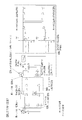
- the mechanical configuration of the electric working machine 1 will be described with reference to FIGS. 1 to 7.
- FIGS. 1 to 3 and 5 define the front-back, up-down, and left-right directions that are orthogonal to each other.
- the front-rear direction is the working direction of the electric work machine 1.
- the vertical direction is the direction perpendicular to the base 30.
- the left-right direction is defined based on the case of looking at the front direction (cutting progress direction).
- FIGS. 1 and 5 show a state in which the battery pack 51 is attached to the electric work machine 1
- FIGS. 3 and 4 show a state in which the battery pack 51 is not attached to the electric work machine 1.
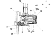
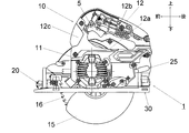
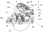
- the electric working machine 1 is a portable circular saw (portable cutting machine) here, and includes a main body 10 and a base 30.
- the main body 10 is connected and supported to the base 30 by a well-known tilt support mechanism 20 and a swing support mechanism 25.
- the main body 10 can be tilted in at least one direction to the left or right with respect to the base 30 by the support of the tilt support mechanism 20. Further, the main body 10 can swing in the vertical direction with respect to the base 30 by the support of the swing support mechanism (cut depth adjusting mechanism) 25.
- the base 30 is a substantially rectangular plate made of metal such as aluminum.
- the longitudinal direction of the base 30 coincides with the working direction of the electric work machine 1.
- the bottom surface of the base 30 is a sliding surface with a work material.
- the housing (outer shell) of the main body 10 is composed of a motor housing 11, a handle housing 12, and a gear cover 13 that are combined and integrated with each other.
- the motor housing 11 is, for example, a resin molded body, and houses the motor 6 shown in FIG. 2 inside.
- the motor 6 is an inner rotor type brushless motor, and has a rotor core 6b made of a magnetic material that rotates integrally with the output shaft 6a around the output shaft 6a.
- a rotor magnet (permanent magnet) 6c is inserted and held in the rotor core 6b.
- a plurality (for example, four) of rotor magnets 6c are provided at equal intervals (for example, 90 degree intervals) in the axial direction.
- a stator core 6d is provided around the rotor core 6b (fixed to the motor housing 11).
- a stator coil 6e (FIG. 7) is provided on the stator core 6d.
- An inverter circuit board 44 is provided on the left side of the stator core 6d substantially perpendicular to the output shaft 6a.
- a plurality of (for example, six) FETs, switching elements 44a such as IGBTs, etc. are mounted on the inverter circuit board 44.
- the switching element 44a corresponds to the switching elements Q1 to Q6 shown in FIG.
- the stator core 6d has a plurality (for example, six) tooth portions that serve as winding axes of the stator coil 6e at equal intervals (for example, 60 degree intervals) in the axial direction.
- each tooth portion is designated as U1, U2, V1, V2, W1, and W2.
- a U-phase stator coil 6e (hereinafter also referred to as "U-phase stator coil”) is wound around the teeth portions U1 and U2, and a V-phase stator coil 6e (hereinafter also referred to as "V-phase stator coil”) is wound around the teeth portions V1 and V2. (Notation) is wound, and a W-phase stator coil 6e (hereinafter, also referred to as “W-phase stator coil”) is wound around the teeth portions W1 and W2.
- Hall IC42 as a rotation position detection unit is arranged between the teeth portions V1 and U1, between the teeth portions U1 and W2, and between the teeth portions W2 and V2, respectively.
- the hole ICs 42 are arranged close to the outer peripheral surface of the rotor core 6b, and three hole ICs 42 are provided at intervals of 60 degrees in the axial direction of the motor 6.
- the rotor rotation position in FIG. 7 is a rotation position in which the axial position of the center hole IC 42 and the central axial position between the adjacent rotor magnets 6c coincide with each other, and is a reference position for the advance angle. At the same time, it corresponds to a rotor rotation angle of 0 degrees.
- the advance angle is the difference between the reference position shown in FIG. 7 and the rotor rotation position at which energization of the U-phase stator coil is started. ..
- the definition of forward rotation is that the rotation direction set by the electric work machine 1 and the actual rotation direction are the same.
- the definition of reversal is that the rotation direction set by the electric work machine 1 and the actual rotation direction are different.
- FIG. 7 defines the right-handed rotation and the left-handed rotation of the motor 6.
- the three hall IC 42s are marked separately from H1, H2, and H3, respectively. In the following, when the three Hall ICs 42 are treated separately, they are designated by the respective reference numerals H1, H2, and H3.
- the handle housing 12 is, for example, a resin molded body having a left-right two-divided structure, and is connected to the gear cover 13.
- the handle housing 12 is connected to the motor housing 11 and the gear cover 13 and connects the base portion 12a for accommodating the control board 41 (FIG. 4), the handle portion 12b serving as the grip portion, and the front end portion and the base portion 12a of the handle portion 12b.
- the connecting portion 12c which is to be used, is included.
- An operation panel 17 is provided on the upper surface of the base portion 12a.
- the rear end of the base 12a and the rear end of the handle 12b are connected to each other.
- the handle portion 12b is provided with a trigger switch (operation portion) 5 for the user to switch between driving and stopping the motor.
- the contact portion of the trigger switch 5 is provided in the handle portion 12b. Regarding the trigger switch 5, operating (pulling) is turning on, and releasing (releasing) the operation is turning off.
- a battery pack 51 (FIGS. 1 and 5) is slidably attached to the rear end of the handle housing 12 so as to be detachable from the rear.
- the operation panel 17 includes a mode changeover switch 17a, a mode display LED 17b, a light lighting switch 17c, a light state display LEDs 17d and 17e, a silent mode switch 17f, and a silent mode display LED 17g.
- the mode changeover switch 17a is a switch in which the operator switches the operation mode of the electric work machine 1 between the normal mode and the high-speed mode, which will be described later.
- the high-speed mode may be a mode that is effective only when a battery pack 51 having a rated voltage of 14.4 V (a battery pack 51 having a low rated voltage) is attached.
- the switching of the operation mode by the mode changeover switch 17a may be effective only when the battery pack 51 having the rated voltage of 14.4 V is attached.
- the normal mode is a mode that is effective regardless of the rated voltage of the battery pack 51.
- the mode display LED 17b is a notification unit that notifies the operation mode of the electric work machine 1, and is turned on, for example, in the high-speed mode and turned off in the normal mode.
- the light lighting switch 17c is a switch in which the operator switches on and off the LED light 49 (FIG. 8) that irradiates the work material with light.
- the light status display LEDs 17d and 17e are notification units that notify the lighting status of the LED light 49.
- the silent mode switch 17f is a switch for setting the operation mode of the electric work machine 1 to the silent mode.
- the silent mode display LED 17g is turned on, for example, in the silent mode, and turned off in other cases.
- the gear cover 13 is made of metal such as aluminum and is connected to the handle housing 12.
- the gear cover 13 covers the speed reduction mechanism 8 (FIG. 2) that decelerates the rotation of the motor 6 and transmits it to the saw blade 16, and also covers the upper half of the saw blade 16.
- the protective cover 15 is, for example, a resin molded body, and covers the lower half of the saw blade 16 so as to be openable and closable.
- the saw blade 16 as a tip tool (rotating tool) is a disk-shaped rotary blade, which is rotationally driven by a motor 6. The saw blade 16 projects downward from the lower surface of the base 30.
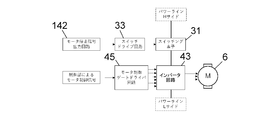
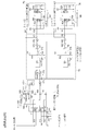
- FIG. 8 is a circuit block diagram of the electric work machine 1.
- the first control unit 40 and the second control unit 50 are mounted on the control board 41 shown in FIG.
- the first control unit 40 and the second control unit 50 may be mounted on different substrates.
- the first control unit 40 performs various controls such as drive control of the inverter circuit 43.
- the inverter circuit 43 is an example of the first cutoff unit.
- the first control unit 40 and the second control unit 50 detect a rotation abnormality of the motor 6, and when the rotation abnormality of the motor 6 is detected, control to cut off the power path to the motor 6.
- the control of the first control unit 40 includes software processing by the calculation unit 34, that is, execution of a pre-stored program.
- the control of the second control unit 50 is realized only by hardware processing, not by software.
- the second control unit 50 is realized by a combination of digital circuits such as various logic circuits and analog circuits such as resistors and capacitors (capacities).
- the abnormal rotation of the motor 6 is caused by the over-rotation of the motor 6, the reverse rotation of the motor 6 with respect to the set rotation direction, the stop of the motor 6 when the trigger switch 5 is on, and the motor 6 when the trigger switch 5 is off. Including rotation.
- the case where the motor is rotating in the working direction is the direction in which the saw blade 16 of the portable circular saw (portable cutting machine) cuts the mating material in the present embodiment, and is counterclockwise in FIG. It is the direction of rotation.
- the rotation direction set by the switching unit for switching between forward rotation and reverse rotation corresponds to the working direction. Further, satisfying the predetermined condition is a state of abnormal rotation of the motor 6 described above.
- the inverter circuit 43 as a drive circuit includes switching elements Q1 to Q6 such as IGBTs and FETs connected by a three-phase bridge.
- the switching elements Q1 to Q6 perform a switching operation according to the control of the first control unit 40 to supply a drive current to the stator coil 6e (each winding of U, V, W) of the motor 6.
- the resistors Rs are provided in the path of the current of the motor 6 (hereinafter, also referred to as “motor current”).
- the cutoff circuit 31 as the second cutoff unit is provided in the motor current path (power path to the motor 6).
- the cutoff circuit 31 is a switch that can be electrically opened and closed, such as a relay or a switching element.
- the control power supply circuit 46 converts the voltage of the battery pack 51 into a voltage suitable for the operation of the first control unit 40 and the second control unit 50, and supplies the voltage to the first control unit 40 and the second control unit 50.
- the hall IC 42 outputs a signal corresponding to the rotation position (rotor rotation position) of the motor 6.
- the various switches 17a, 17c, and 17f shown in FIG. 8 are blocks in which the mode changeover switch 17a, the light lighting switch 17c, and the silent mode switch 17f shown in FIG. 6 are put together.
- the LED light 49 is, for example, a light that irradiates a work material with light, and when the light lighting switch 17c shown in FIG. 6 is turned on, the LED light 49 is turned on by an LED drive circuit 32 that operates under the control of the calculation unit 34.
- the LED light 49 also functions as an abnormality notification unit that notifies the user by blinking or the like when a rotation abnormality of the motor 6 occurs.
- the current detection circuit 37 detects the drive current (load) of the motor 6 by the voltage across the detection resistor Rs and transmits it to the calculation unit 34.
- the switch detection circuit 38 detects the operation of the trigger switch 5 by the user and transmits it to the calculation unit 34.
- the voltage detection circuit 39 detects the output voltage of the battery pack 51 and transmits it to the calculation unit 34.
- the rotor position detection circuit 35 detects the rotation position of the motor 6 based on the signal (position signal) from the hall IC 42 and transmits it to the calculation unit 34.
- the calculation unit 34 includes a microcontroller and the like, and stores the control program of the motor 6 in advance.
- the calculation unit 34 drives the gate driver circuit 45 by performing rotation speed calculation and commutation phase selection according to the rotation position of the motor 6 detected by the rotor position detection circuit 35.
- the switching elements Q1 to Q6 of the inverter circuit 43 are switched controlled (for example, PWM control) by the output signal of the gate driver circuit 45.
- the calculation unit 34 can further detect the rotation speed of the saw blade 16 from the detection result of the rotor position detection circuit 35 based on the set reduction ratio of the motor 6 and the saw blade 16. When the calculation unit 34 detects a rotation abnormality of the motor 6, it controls to apply an off signal (first signal) from the gate driver circuit 45 to the inverter circuit 43.
- the second control unit 50 includes an over-rotation detection circuit (over-rotation detection unit) 60, a rotation / stop detection circuit 70, a rotation direction detection circuit (rotation direction detection unit) 90, a stop detection circuit 100 when the trigger is turned on, and the like. It includes a rotation detection circuit 120 when the trigger is off, a rotation abnormality detection circuit 130, and a cutoff signal output / self-reset prevention circuit 140.
- the rotation / stop detection circuit 70, the stop detection circuit 100 when the trigger is ON, and the rotation detection circuit 120 when the trigger is OFF constitute a rotation stop detection unit.
- the over-rotation detection circuit 60 is a circuit that detects the over-rotation of the motor 6 by using the output signal of any of the hall ICs 42. Over-rotation means that the motor 6 rotates at a rotation speed equal to or higher than the over-rotation threshold value (over-rotation set value).
- the rotation / stop detection circuit 70 is a circuit that detects whether the motor 6 is rotating or stopped by using the output signals of the three hall ICs 42.
- the rotation direction detection circuit 90 is a circuit that detects the rotation direction of the motor 6 by using the output signals of the three hall ICs 42.
- the stop detection circuit 100 when the trigger is ON is a circuit that detects the stop (unintended stop) of the motor 6 when the trigger switch 5 is ON.
- the rotation detection circuit 120 when the trigger is OFF is a circuit that detects the rotation (unintended rotation) of the motor 6 when the trigger switch 5 is OFF.
- the rotation abnormality detection circuit 130 is the over-rotation of the motor 6, the reverse rotation of the motor 6 with respect to the set rotation direction, the stop of the motor 6 when the trigger switch 5 is ON, or the motor 6 when the trigger switch 5 is OFF. This circuit outputs a rotation abnormality detection signal when rotation is detected.
- the cutoff signal output / self-reset prevention circuit 140 is a circuit that outputs a cutoff signal to the cutoff circuit 31 when it receives a rotation abnormality detection signal.
- the cutoff signal output / self-reset prevention circuit 140 is also a circuit that transmits a reset signal to the rotation abnormality detection circuit 130 when the OFF state of the trigger switch 5 is detected after the rotation abnormality is resolved.
- the rotation abnormality detection circuit 130 sets the reception of the reset signal as a condition for stopping the output of the rotation abnormality detection signal. That is, the reset signal has a function of preventing the self-reset of the rotation abnormality detection circuit 130.
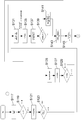
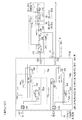
- FIG. 10 is a block diagram of the over-rotation detection circuit 60 of FIG.
- the over-rotation detection circuit 60 includes a frequency dividing circuit 61, a rising edge detection circuit 62, a timer IC (timekeeping circuit) 63, a comparison circuit 64, an over-rotation state detection / storage circuit 65, and an over-rotation state reset circuit 66. And, including.
- the frequency dividing circuit 61 divides the frequency of the output signal of the Hall ICH2 by a predetermined ratio.
- the frequency dividing circuit 61 has a role of improving the measurement accuracy by adjusting the period of the output signal of the Hall ICH2 to an appropriate length.
- the frequency dividing circuit 61 may be omitted.
- the rising edge detection circuit 62 detects the rising edge of the output signal of the frequency dividing circuit 61
- the rising edge detection circuit 62 outputs a rising edge detection signal.
- the rising edge detection signal is, for example, a short-time pulse signal.
- the timer IC 63 When the timer IC 63 receives the rising edge detection signal, it outputs a signal that becomes a high level only during the over-rotation determination threshold time. If the next rising edge of the frequency dividing circuit 61 occurs within the over-rotation determination threshold time, it is determined that the over-rotation is over-rotation.
- the comparison circuit 64 compares the time when the output signal of the timer IC 63 is at a high level (over-rotation determination threshold time) and the time until the next rising edge detection signal (measurement time). The comparison circuit 64 outputs an error detection signal when the measurement time is shorter than the over-rotation determination threshold time.
- the over-rotation state detection / storage circuit 65 When the over-rotation state detection / storage circuit 65 receives the error detection signal, it detects and stores that the motor 6 is in the over-rotation state, and outputs the over-rotation signal. When the over-rotation state reset circuit 66 receives the stop confirmation signal indicating the stop of the motor 6 from the stop detection circuit 80 described later, the over-rotation state reset circuit 66 transmits the reset signal to the over-rotation state detection / storage circuit 65. When the over-rotation state detection / storage circuit 65 receives the reset signal, the over-rotation state detection / storage circuit 65 detects that the motor 6 is in the over-rotation state and cancels the storage.
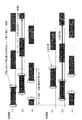
- FIG. 11 is a time chart showing a state change related to the detection of over-rotation of the motor 6.
- FIG. 12 is an enlarged view of part A of FIG.
- the output signal of the timer IC 63 rises together with the rising edge of the output signal of the frequency dividing circuit 61.
- the output signal of the timer IC 63 is at a high level only during the over-rotation determination threshold time, and returns to a low level when the over-rotation determination threshold time elapses.
- time t4 after the output signal of the timer IC 63 returns to the low level, the next rising edge of the output signal of the frequency dividing circuit 61 occurs.
- the rising edge of the output signal of the frequency dividing circuit 61 occurs while the output signal of the timer IC 63 is at a high level.
- the over-rotation state detection / storage circuit 65 outputs an over-rotation signal (sets the over-rotation signal to a high level).
- the output signal of the hall ICH1 or the hall ICH3 may be used instead of the hall ICH2.
- FIG. 13 is a block diagram of the rotation / stop detection circuit 70 of FIG.
- the rotation / stop detection circuit 70 includes a double-edge detection circuit 71, a timer IC selection circuit 72, timer ICs (timekeeping circuits) 73 and 74, a comparison circuit 75, a rotation detection circuit 76, and a rotation counter circuit 77. It includes a rotation state detection circuit 78, a rotation state storage circuit 79, a stop detection circuit 80, a counter reset circuit 81, and a rotation state reset circuit 82.
- the both edge detection circuits 71 detect the rising edge and the falling edge of the output signals of the halls ICH1 to H3, and output the edge detection signal.
- the edge detection signal is, for example, a short-time pulse signal.
- the timer IC selection circuit 72 is a circuit that selectively transmits an edge detection signal to any of the timer ICs 73 and 74. Specifically, each time the timer IC selection circuit 72 receives the edge detection signal, the timer IC selection circuit 72 alternately transmits the edge detection signal to the timer ICs 73 and 74.
- the timer ICs 73 and 74 When the timer ICs 73 and 74 receive the edge detection signal from the timer IC selection circuit 72, the timer ICs 73 and 74 output a high level signal only during the rotation determination threshold time. When the event that the edge detection signal is generated during the rotation determination threshold time occurs a predetermined number of times, it is determined that the motor 6 is rotating. If the edge detection signal is not generated during the rotation determination threshold time, it is determined that the motor 6 is stopped.
- the comparison circuit 75 compares the time when the output signal of any of the timer ICs 73 and 74 is at a high level (rotation determination threshold time) and the time until the next edge detection signal (measurement time).
- the comparison circuit 75 outputs a rotation detection signal when the measurement time is shorter than the rotation determination threshold time.
- the comparison circuit 75 outputs a stop detection signal when the measurement time is longer than the rotation determination threshold time.
- the rotation detection circuit 76 When the rotation detection circuit 76 receives the rotation detection signal (when the measurement time is shorter than the rotation determination threshold time), the rotation counter circuit 77 counts up. When the count value of the rotation counter circuit 77 reaches a predetermined number, the rotation state detection circuit 78 detects that the motor 6 is in the rotation state. The rotation state storage circuit 79 stores that the motor 6 is in the rotation state. When the stop detection circuit 80 receives the stop detection signal (when the measurement time is longer than the rotation determination threshold time), the stop detection circuit 80 detects that the motor 6 is in the stopped state and outputs a stop confirmation signal. Upon receiving the stop confirmation signal, the counter reset circuit 81 resets the rotation counter circuit 77 (sets the count value to 0).
- the counter reset circuit 81 resets the rotation counter circuit 77 when it receives a rotation direction change detection signal from the rotation direction change detection circuits 96a to 96c described later.
- the rotation state reset circuit 82 Upon receiving the stop confirmation signal, the rotation state reset circuit 82 resets the rotation state storage circuit 79 (releases the memory that the motor 6 is in the rotation state).
- FIG. 14 is a time chart showing state changes related to rotation detection and stop detection of the motor 6.
- FIG. 15 is an enlarged view of part B of FIG.
- the edge detection signal is a pulse signal that drops to a low level for a short time. Then, when the edge detection signal is output while the output signal of any of the timer ICs 73 and 74 is at a high level, the rotation counter circuit 77 counts up. In the example of FIG. 15, when the count value of the rotation counter circuit 77 reaches 3, it is detected that the motor 6 is in the rotating state. The rotation counter circuit 77 overflows at the fourth count and the count value returns to 0, but the detection that the motor 6 is in the rotating state is maintained.
- the output signals of the timers ICs 73 and 74 are reset (return to the low level) if there is an edge detection signal while the level is high.
- FIG. 16 is an enlarged view of part C of FIG.
- the edge detection signal before time t7 is generated while the output signal of any of the timer ICs 73 and 74 is at a high level.
- the edge detection signal at time t7 is generated after the output signal of the timer IC 73 becomes low level.
- the stopped state of the motor 6 is not only when the motor 6 is completely stopped, but also when the motor 6 is slowly rotating by hand rotation of the saw blade 16 (when the motor 6 is rotating below the stop determination rotation speed). Is also detected.
- FIG. 17 is a time chart showing a case where the stop of the motor 6 cannot be detected when one timer IC is used in FIG.
- the motor 6 is completely stopped by an external force or the like before it starts up by the next edge detection signal.
- the output signal of the timer IC does not rise. Then, it remains detected that the motor 6 is in the rotating state, and the stop detection of the motor 6 cannot be performed. The error canceled by the stop detection of the motor 6 cannot be canceled.
- FIG. 18 is a time chart showing that the stop of the motor 6 can be detected even in the same case as in FIG. 17 because there are two timer ICs in FIG.
- the output signal of one of the timer ICs is time-measured at a high level. Therefore, the stop detection of the motor 6 can be reliably performed.
- FIG. 19 is a block diagram of the rotation direction detection circuit 90 of FIG.
- the rotation direction detection circuit 90 includes both edge detection circuits 91a to 91c, edge direction detection circuits 92a to 92c, a set rotation direction detection circuit 93, a hall IC comparison selection circuit 94a to 94c, and a rotation direction detection circuit (undetermined). ) 95a to 95c, rotation direction change detection circuits 96a to 96c, rotation direction determination circuit 97, rotation direction reset circuit 98, and rotation direction storage circuit 99.
- the both edge detection circuits 91a to 91c detect the rising edge and the falling edge of each output signal of the halls ICH1 to H3, and output the edge detection signal.
- the edge detection signal is, for example, a short-time pulse signal.
- the edge direction detection circuits 92a to 92c detect whether the detected edge is a rising edge or a falling edge, respectively.
- the set rotation direction detection circuit 93 detects the current set rotation direction of the motor 6 and inputs it to the Hall IC comparison selection circuits 94a to 94c. In the figure, the signal lines from the set rotation direction detection circuit 93 to the Hall IC comparison selection circuits 94b and 94c are omitted.
- the set rotation direction detection circuit 93 is unnecessary.
- the set rotation direction is assumed to be clockwise.
- the Hall IC comparison and selection circuits 94a to 94c select one of the Hall ICs according to the set rotation direction and the edge direction, respectively, and detect the level of the output signal of the Hall IC.
- the rotation direction detection circuits (undetermined) 95a to 95c detect whether the level of the output signal of the Hall IC selected by the Hall IC comparison selection circuits 94a to 94c matches the current set rotation direction. If it matches, it is detected as normal rotation, and if it does not match, it is detected as reverse rotation.
- the rotation direction change detection circuits 96a to 96c output a rotation direction change detection signal when there is a change in the rotation direction detected by the rotation direction detection circuits (undetermined) 95a to 95c.
- the rotation direction determination circuit 97 deterministically detects the rotation direction of the motor 6 by the output signals of the rotation direction detection circuits (undetermined) 95a to 95c, the rotation direction change detection circuits 96a to 96c, and the rotation state detection circuit 78. ..
- the rotation direction storage circuit 99 stores the rotation direction determined by the rotation direction determination circuit 97.
- the rotation direction storage circuit 99 outputs a reverse rotation detection signal when the determined rotation direction is different from the set rotation direction (in the case of reverse rotation).
- the rotation direction storage circuit 99 When the rotation direction storage circuit 99 stores the reverse rotation, the rotation direction storage circuit 99 maintains the reverse rotation storage and continues to output the reverse rotation detection signal even if the rotation direction determination circuit 97 subsequently detects the forward rotation.
- the rotation direction reset circuit 98 receives the stop confirmation signal from the stop detection circuit 80, the rotation direction storage circuit 98 resets the rotation direction storage circuit 99 (releases the reverse rotation if it is stored).
- FIG. 20 to 23 are time charts showing state changes related to the detection of the rotation direction of the motor 6.
- FIG. 20 shows the detection operation based on the hall ICH1
- FIG. 21 shows the detection operation based on the hall ICH2
- FIG. 22 shows the detection operation based on the hall ICH3.
- FIG. 23 shows an operation of determining the rotation direction from the results based on the halls ICH1 to H3, respectively.
- the rotation direction detection circuit (undetermined) 95a detects the normal rotation of the motor 6, the output signal of the hall ICH2 is at a high level (at the timing of the rising edge of the output signal of the hall ICH1). Alternatively, the output signal of the hall ICH3 is low level). Then, the rotation direction detection circuit (undetermined) 95a switches to the reverse rotation detection of the motor 6, and the rotation direction change detection circuit 96a outputs a rotation direction change detection signal.
- the rotation direction change detection signal is, for example, a short-time pulse signal.
- the rotation direction detection circuit (undetermined) 95a detects the reversal of the motor 6, the output signal of the hall ICH2 is at a low level (or at the timing of the rising edge of the output signal of the hall ICH1). The output signal of the hall ICH3 is high level). Then, the rotation direction detection circuit (undecided) 95a switches to the normal rotation detection of the motor 6, and the rotation direction change detection circuit 96a outputs a rotation direction change detection signal.
- the rotation direction detection circuit (undetermined) 95b detects the forward rotation of the motor 6, the output signal of the hall ICH1 is at a high level at the timing of the falling edge of the output signal of the hall ICH2. (Or the output signal of Hall ICH3 is low level). Then, the rotation direction detection circuit (undetermined) 95b switches to the reverse rotation detection of the motor 6, and the rotation direction change detection circuit 96b outputs a rotation direction change detection signal.
- the rotation direction detection circuit (undetermined) 95b detects the reversal of the motor 6, the output signal of the hall ICH3 is at a low level (or at the timing of the rising edge of the output signal of the hall ICH2). The output signal of the hall ICH1 is high level). Then, the rotation direction detection circuit (undetermined) 95b switches to the normal rotation detection of the motor 6, and the rotation direction change detection circuit 96b outputs a rotation direction change detection signal.
- the rotation direction detection circuit (undetermined) 95c detects the normal rotation of the motor 6, the output signal of the hall ICH1 is at a high level (at the timing of the rising edge of the output signal of the hall ICH3). Alternatively, the output signal of the hall ICH2 is low level). Then, the rotation direction detection circuit (undetermined) 95b switches to the reverse rotation detection of the motor 6, and the rotation direction change detection circuit 96b outputs a rotation direction change detection signal.
- the rotation direction detection circuit (undetermined) 95c detects the reversal of the motor 6, the output signal of the hall ICH2 is at a low level (at the timing of the falling edge of the output signal of the hall ICH3).
- the output signal of the hall ICH1 is at a high level). Then, the rotation direction detection circuit (undecided) 95c switches to the normal rotation detection of the motor 6, and the rotation direction change detection circuit 96c outputs a rotation direction change detection signal.
- a rotation direction change detection signal is output when the rotation direction determination circuit 97 detects normal rotation. Then, the count value of the rotation counter circuit 77 is reset. When the count value of the rotation counter circuit 77 becomes 3 at the subsequent time t15, the rotation direction determination circuit 97 switches to reverse rotation detection, and the rotation direction storage circuit 99 outputs a reverse rotation detection signal (set to a high level). At time t16, the rotation direction change detection signal is output when the rotation direction determination circuit 97 detects the reverse rotation. Then, the count value of the rotation counter circuit 77 is reset. When the count value of the rotation counter circuit 77 becomes 3 at the subsequent time t17, the rotation direction determination circuit 97 switches to normal rotation detection. When the stop of the motor 6 is detected at time t18, the rotation direction storage circuit 99 is reset by the rotation direction reset circuit 98, and the reverse rotation detection signal stops (becomes a low level).
- FIG. 24 is a block diagram of the stop detection circuit 100 when the trigger is turned on in FIG.
- the trigger ON stop detection circuit 100 includes a trigger operation detection circuit 101, a trigger operation rotation state detection circuit 102, a trigger operation rotation state storage circuit 103, a timer IC measurement start timing setting circuit 104, and a timer IC (time counting). Circuit) 105, a trigger state detection circuit 106, an unintended stop detection circuit 107, an unintended stop storage circuit 108, a trigger release detection circuit 109, and an unintended stop reset circuit 110.
- the trigger operation detection circuit 101 detects the turn-on of the trigger switch 5 and outputs a turn-on detection signal.
- the rotation state detection circuit 102 during trigger operation detects whether or not the motor 6 is rotating when the turn-on detection signal is received (when the trigger switch 5 is operated).
- the rotation state storage circuit 103 at the time of trigger operation stores the presence / absence of rotation of the motor 6 when the trigger switch 5 is operated.
- the timer IC measurement start timing setting circuit 104 sets the measurement start timing of the timer IC 105 according to the presence or absence of rotation of the motor 6 when the trigger switch 5 is operated. For example, the measurement start timing is the timing at which the trigger switch 5 is operated if the motor 6 is stopped when the trigger switch 5 is operated.
- the measurement start timing is the timing at which a predetermined standby time has elapsed since the trigger switch 5 is operated, or a stop confirmation signal is sent from the stop detection circuit 80. It is the timing of reception.
- the predetermined standby time is the time until the motor 6 is stopped when no rotational force is applied to the motor 6.
- the timer IC 105 starts measurement according to the set measurement timing. The timer IC 105 outputs a high level signal only during the start time threshold from the start of measurement.
- the trigger state detection circuit 106 detects the current state of the trigger switch 5.
- the unintended stop detection circuit 107 detects an unintended stop of the motor 6 (stop of the motor 6 when the trigger switch 5 is turned on) based on the signals from the timer IC 105, the trigger state detection circuit 106, and the stop detection circuit 80. ..
- the unintended stop detection circuit 107 detects an unintended stop unless the stop detection state of the motor 6 is released within the measurement time by the timer IC 105. Further, when the unintended stop detection circuit 107 detects that the motor 6 has stopped while the trigger switch 5 is on, it detects that the motor 6 has stopped unintentionally.
- the unintended stop storage circuit 108 stores an unintended stop state when an unintended stop is detected by the unintended stop detection circuit 107.
- the trigger release detection circuit 109 detects the turn-off of the trigger switch 5 and outputs a turn-off detection signal.
- the unintended stop reset circuit 110 resets the unintended stop storage circuit 108.
- 25 to 27 are time charts showing state changes related to stop detection of the motor 6 when the trigger switch 5 is ON.
- 25 and 26 show the operation when the motor 6 is stopped when the trigger switch 5 is operated.
- FIG. 27 shows the operation when the motor 6 is rotating when the trigger switch 5 is operated.
- the motor 6 is successfully started when the trigger switch 5 is turned on, but the motor 6 is stopped with the trigger switch 5 turned on at the subsequent time t21.
- the unintended stop storage circuit 108 outputs an unintended stop detection signal (set to a high level).
- the unintended stop storage circuit 108 is reset and the unintended stop detection signal is stopped (low level).
- FIG. 25 and 26 show the operation when the motor 6 is stopped when the trigger switch 5 is operated.
- FIG. 27 shows the operation when the motor 6 is rotating when the trigger switch 5 is operated.
- the motor 6 is successfully started when the trigger switch 5 is turned on, but the motor 6 is stopped with the trigger switch 5 turned on at the subsequent time t21.
- the motor 6 does not rotate even if the trigger switch 5 is turned on at time t23.
- the stopped state of the motor 6 is not resolved even at the time t24 when the measurement time (starting time threshold value) by the timer IC 105 has elapsed. Therefore, at time t24, the unintended stop storage circuit 108 outputs an unintended stop detection signal.
- the motor 6 is already rotating when the trigger switch 5 is turned on at time t25. Therefore, the timer IC 105 waits until the stop confirmation signal of the motor 6 is received at time t26, and then starts the measurement.
- the stopped state of the motor 6 is not resolved even at the time t27 when the measurement time has elapsed. Therefore, at time t27, the unintended stop storage circuit 108 outputs an unintended stop detection signal.
- FIG. 28 is a block diagram of the rotation detection circuit 120 when the trigger is OFF in FIG.
- the rotation detection circuit 120 when the trigger is OFF includes a trigger release detection circuit 121, a timer IC (timekeeping circuit) 122, an unintended rotation detection circuit 123, an unintended rotation storage circuit 124, a trigger state detection circuit 125, and an unintended one.
- the rotation reset circuit 126 and the like are included.
- the trigger release detection circuit 121 detects the turn-off of the trigger switch 5 and outputs a turn-off detection signal.
- the timer IC 122 starts time measurement when it receives the turn-off detection signal.
- the timer IC 122 outputs a high level signal only during the inertial rotation standby time threshold value from the start of measurement.
- the trigger state detection circuit 125 detects the current state of the trigger switch 5.
- the unintended rotation detection circuit 123 detects the unintended rotation of the motor 6 (rotation of the motor 6 when the trigger switch 5 is off) based on the signals from the timer IC 122, the trigger state detection circuit 125, and the rotation state storage circuit 79. To do.
- the unintended rotation detection circuit 123 detects that the rotation is unintended if the motor 6 is stopped within the measurement time by the timer IC 122. Further, the unintended rotation detection circuit 123 detects an unintended rotation when the stop detection state of the motor 6 is released while the trigger switch 5 is off. When an unintended rotation is detected, the unintended rotation storage circuit 124 stores an unintended rotation state. When the unintended rotation reset circuit 126 receives the stop confirmation signal from the stop detection circuit 80, the unintended rotation reset circuit 126 resets the unintended rotation storage circuit 124.
- 29 and 30 are time charts showing state changes related to rotation detection of the motor 6 when the trigger switch 5 is OFF.
- the motor 6 is successfully stopped due to the turn-off of the trigger switch 5, but the motor 6 rotates with the trigger switch 5 turned off at the subsequent time t31.
- the unintended rotation detection circuit 123 outputs an unintended rotation detection signal (set to a high level).
- the unintended rotation storage circuit 124 is reset and the unintended rotation detection signal is stopped (low level).
- FIG. 29 and 30 are time charts showing state changes related to rotation detection of the motor 6 when the trigger switch 5 is OFF.
- the motor 6 does not stop between the time t33 when the trigger switch 5 is turned off and the time t34 when the inertial rotation standby time threshold value elapses. Therefore, at time t34, the unintended rotation storage circuit 124 outputs an unintended rotation detection signal. When the stop of the motor 6 is detected at the subsequent time t35, the unintended rotation storage circuit 124 is reset and the unintended rotation detection signal is stopped.
- FIG. 31 is a block diagram of the rotation abnormality detection circuit 130 and the cutoff signal output / self-reset prevention circuit 140 of FIG.
- the rotation abnormality detection circuit 130 includes an abnormal state integrated storage circuit 131 and an abnormal state integrated reset circuit 132.
- the cutoff signal output / self-reset prevention circuit 140 includes a trigger state detection circuit 141 and a motor stop signal output circuit 142.
- the abnormal state integrated storage circuit 131 includes an over-rotation signal from the over-rotation state detection / storage circuit 65, a reverse rotation detection signal from the rotation direction storage circuit 99, an unintended stop detection signal from the unintended stop storage circuit 108, and an intention.
- the motor 6 When at least one of the unintended rotation detection signals from the rotation storage circuit 124 is received (at least one becomes high level), the motor 6 is stored in an abnormal state and an abnormality detection signal is output.
- the motor stop signal output circuit 142 receives the abnormality detection signal, it outputs a cutoff signal to the cutoff circuit 31 to cut off the power path to the motor 6.
- the trigger state detection circuit 141 detects the current state of the trigger switch 5.
- the abnormal state integrated reset circuit 132 resets the abnormal state integrated storage circuit 131.
- 32 to 34 are block diagrams showing configuration examples relating to interruption of the power path to the motor 6, respectively.
- 32 is an example corresponding to FIG. 8, and FIGS. 32 and 34 are modifications with respect to FIG.
- the cutoff circuit 31 is a switching element provided in the power path on the high side side of the inverter circuit 43.
- the cutoff circuit 31 is a switching element provided in the power path on the low side of the inverter circuit 43.
- the switch drive circuit 33 turns off the cutoff circuit 31 when it receives the cutoff signal from the motor stop signal output circuit 142.
- the cutoff circuit 31 is an output permission / non-permission detection circuit provided in the path of the drive signal from the calculation unit 34 to the gate driver circuit 45.
- the cutoff circuit 31 receives the cutoff signal from the motor stop signal output circuit 142, the cutoff circuit 31 cuts off the drive signal from the calculation unit 34 to the gate driver circuit 45.
- the inverter circuit 43 is turned off, and the power path to the motor 6 is cut off.
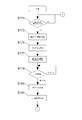
- FIG. 35 is a flowchart showing an operation related to overrotation detection of the motor 6.
- Time has passed from the rotation of the motor 6 (S1) (S3), and the rising edge detection circuit 62 detects the rising edge of the hall ICH2 (S5).
- the rising edge detection circuit 62 detects the rising edge of the output signal of the frequency dividing circuit 61.
- the timer IC 63 starts outputting a pulse signal that becomes a high level for the over-rotation determination threshold time at the timing of the rising edge detection in step S5 (S7).
- the rising edge detection circuit 62 detects the rising edge next to the output signal of the Hall ICH2 (S11).
- the comparison circuit 64 detects whether or not the pulse signal of the timer IC 63 is output at the time of detecting the rising edge in step S11 (S13). If no pulse signal is output (No in S13), the over-rotation state detection / storage circuit 65 detects that the motor 6 has a normal rotation speed (S15). If the pulse signal is output (Yes in S13), the over-rotation state detection / storage circuit 65 detects that the motor 6 is in the over-rotation state and stores it (S17). Upon receiving the stop confirmation signal from the stop detection circuit 80, the over-rotation state reset circuit 66 resets the over-rotation state detection / storage circuit 65 to eliminate the over-rotation error (S21). When the over-rotation state detection / storage circuit 65 stores the over-rotation state, the over-rotation state detection / storage circuit 65 maintains the storage of the over-rotation state until it is reset by the over-rotation state reset circuit 66.
- FIG. 36 is a flowchart showing the operation related to the rotation detection and the stop detection of the motor 6.
- Time has passed since the rotation of the motor 6 (S25) (S27), and the both edge detection circuits 71 detect the rising edge or the falling edge of any of the halls ICH1 to H3 (S29).
- the timer IC 73 starts outputting a pulse signal that becomes a high level for the rotation determination threshold time (S31).
- the comparison circuit 75 detects whether or not the pulse signal of the timer IC 74 is output at the time of edge detection in step S29 (S33). If the pulse signal is output (Yes in S33), the rotation detection circuit 76 increments the count value of the rotation counter circuit 77 (S35).
- the rotation state detection circuit 78 detects that the motor 6 is in the rotation state, and the rotation state storage circuit 79 detects that the motor 6 is in the rotation state. Is remembered (S39). If the pulse signal is not output in step S33 (No in S33), the stop detection circuit 80 initializes the count value of the rotation counter circuit 77 (S41). The rotation state reset circuit 82 resets the rotation state storage circuit 79 (S43).
- the both edge detection circuits 71 detect the next rising edge or falling edge of any of Hall ICH1 to H3 (S49). ..
- the timer IC 74 starts outputting a pulse signal having a high level for the rotation determination threshold time at the timing of edge detection in step S49 (S51).
- the comparison circuit 75 detects whether or not the pulse signal of the timer IC 73 is output at the time of edge detection in step S49 (S53). If the pulse signal is output (Yes in S53), the rotation detection circuit 76 increments the count value of the rotation counter circuit 77 (S55).
- the rotation state detection circuit 78 detects that the motor 6 is in the rotation state, and the rotation state storage circuit 79 detects that the motor 6 is in the rotation state. Is remembered (S59). If the pulse signal is not output in step S53 (No in S53), the stop detection circuit 80 initializes the count value of the rotation counter circuit 77 (S61). The rotation state reset circuit 82 resets the rotation state storage circuit 79 (S63). The output of the pulse signal by the timer IC 73 is stopped (S65), and the process returns to step S27.
- FIG. 37 is a flowchart showing an operation related to the detection of the rotation direction of the motor 6.
- the set rotation direction detection circuit 93 detects the set rotation direction of the current motor 6 (S67). Time has passed since the rotation of the motor 6 (S69) (S71), and the both edge detection circuits 91a to 91c detect the rising edge or the falling edge of the halls ICH1 to H3, respectively (S73, S81, S89).
- the Hall IC comparison and selection circuits 94a to 94c determine which Hall IC output signal is to be detected from the edge orientation (rising or falling) detected in steps S73, S81, and S89 and the set rotation direction.
- the rotation direction detection circuits (undecided) 95a to 95c detect that the output signal of the Hall IC and the set rotation direction match (Yes in S97), detect that the motor 6 is rotating in the normal direction (S99), and do not match. (No in S97), it is detected that the motor 6 is reversed (S101).
- the rotation direction change detection circuits 96a to 96c send the rotation direction change detection signal to the counter reset circuit 81.
- the rotation direction determination circuit 97 stores the detected rotation direction of the motor 6 (S107). If the count value by the rotation counter circuit 77 reaches a predetermined value (Yes in S109), the rotation direction determination circuit 97 determines the rotation direction of the motor 6, and the rotation direction storage circuit 99 stores the determined rotation direction (Yes). S111). When the stop detection circuit 80 receives the stop confirmation signal (Yes in S113), the rotation direction reset circuit 98 resets the rotation direction storage circuit 99 (S115).
- FIG. 38 is a flowchart showing an operation related to stop detection of the motor 6 when the trigger switch 5 is ON.
- the trigger operation detection circuit 101 detects the on operation of the trigger switch 5 (“release ⁇ pull” in S117 and S119).
- the first control unit 40 starts drive control of the motor 6 (S121).
- the timer IC 105 waits until it receives a stop confirmation signal from the stop detection circuit 80 (S125).
- the trigger state detection circuit 106 detects the state of the trigger switch 5 (S127).
- the timer IC 105 starts outputting a high level pulse signal only during the start-up time threshold (S131).
- step S123 the timer IC 105 starts outputting the pulse signal at the timing of the turn-on of the trigger switch 5 (“release ⁇ pull” in S119) (S131). .. After the lapse of time (S135), the output of the pulse signal of the timer IC 105 stops (S137). At this time, if the rotation of the motor 6 has not been detected (No in S139), the unintended stop detection circuit 107 detects an unintended stop error of the motor 6, and the unintended stop storage circuit 108 stops the motor 6 unintentionally. Store the error (S141).
- the unintended stop reset circuit 110 resets the unintended stop storage circuit 108 to eliminate the unintended stop error. (S145).
- FIG. 39 is a flowchart showing an operation related to rotation detection of the motor 6 in a state where the trigger switch 5 is OFF.
- the trigger state detection circuit 125 detects the state of the trigger switch 5 (S151).
- the trigger switch 5 is on (“pulling” in S153)
- the trigger release detection circuit 121 detects the turn-off of the trigger switch 5 (S155)
- the timer IC 122 is set to a high level only during the inertial rotation standby time threshold value.
- the output of the pulse signal is started (S157). After the lapse of time (S159), the output of the pulse signal of the timer IC 122 stops (S161).
- the unintended rotation detection circuit 123 detects an unintended rotation error, and the unintended rotation storage circuit 124 stores an unintended rotation error (S165). ).
- the unintended rotation reset circuit 126 receives the stop confirmation signal from the stop detection circuit 80 (Yes in S163), the unintended rotation reset circuit 126 resets the unintended rotation storage circuit 124 and eliminates the unintended rotation error (S167). If the trigger switch 5 is off in step S153 and the pulse signal of the timer IC 122 is not output (“separated and pulse P5 is not output” in S153), the process proceeds to step S163.
- FIG. 40 is a flowchart showing an operation related to rotation abnormality detection and self-reset prevention of the motor 6. If at least one rotation abnormality of the motor 6 is detected (Yes in S171), the abnormal state integrated storage circuit 131 detects and stores the integrated error (S173). The motor stop signal output circuit 142 turns on the motor stop signal (cutoff signal) (S175). When all the rotation abnormalities of the motor 6 are resolved (S177) and the trigger switch 5 is turned off (“separated” in S179), the integrated error of the abnormal state integrated storage circuit 131 is resolved (S181). The motor stop signal output circuit 142 turns off the motor stop signal (S183).
- Both the first control unit 40 and the second control unit 50 detect a rotation abnormality of the motor 6, and when detected, control is performed to cut off the power path to the motor 6. Therefore, it is possible to increase the certainty of protection against the rotation abnormality of the motor 6 as compared with the case where the rotation abnormality of the motor 6 is detected only by the first control unit 40.
- the second control unit 50 detects a rotation abnormality of the motor 6 even if the rotation abnormality of the motor 6 is not detected. Therefore, it is possible to increase the certainty of protection against abnormal rotation of the motor 6.
- the second control unit 50 detects the rotation abnormality of the motor 6 and cuts off the circuit 31. As a result, the power path to the motor 6 can be cut off, and the certainty of protection against abnormal rotation of the motor 6 can be enhanced.
- the second control unit 50 is a self-reset that continues to cut off the power path of the motor 6 by the motor stop signal (cutoff signal) unless the trigger switch 5 is turned off, even if all the rotation abnormalities of the motor 6 are resolved. Has a preventive function. Therefore, it is possible to prevent the motor 6 from suddenly starting to rotate by eliminating all the rotation abnormalities of the motor 6 while the trigger switch 5 is on, which is convenient.
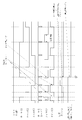
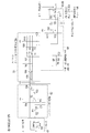
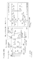
- FIG. 41 shows a specific configuration example of the over-rotation detection circuit 60 shown in FIG.
- the signal of the hall ICH2 is input to the CLK terminal, the D terminal and the inverted Q terminal are connected, and the voltage of the Q terminal is between the high level and the low level each time the signal of the hall ICH2 rises. Switch.
- a signal obtained by halving the frequency of the Hall ICH2 signal is output from the Q terminal, and this signal is input to one input terminal of the AND gate 154.
- the resistor R1 and the capacitor C1 delay the rising edge of the signal at the Q terminal of the D flip-flop 151 according to the time constant, and input the signal to the non-inverting input terminal of the comparator 152.
- the signal at the Q terminal of the D flip-flop 151 changes from high level to low level, the electric charge of the capacitor C1 is discharged via the diode D1 and the resistor R2.
- the resistor R2 a very small resistor (resistor R2 ⁇ resistor R1), the charge of the capacitor C1 can be rapidly consumed, and the input to the non-inverting input terminal of the comparator 152 can be instantly set to 0V. With this configuration, it is possible to keep the rising delay constant even when the signal at the Q terminal of the D flip-flop 151 is switched quickly. As a result, the voltage at the non-inverting input terminal of the comparator 152 becomes low level.
- a voltage obtained by dividing 5V by resistors R4 and R5 is input to the inverting input terminal of the comparator 152.
- the output signal of the comparator 152 rises with a predetermined time delay from the rise of the signal at the Q terminal of the D flip-flop 151.
- the output signal of the comparator 152 is level-inverted by the inverter 153 and input to the other input terminal of the AND gate 154.
- the output signal of the AND gate 154 becomes a high level only from the rising edge of the signal at the Q terminal of the D flip-flop 151 to the rising edge of the output signal of the comparator 152.
- the timer IC 158 outputs a high-level pulse to the OUT terminal for a predetermined time, triggered by the falling edge of the input signal to the TRIG terminal.
- the predetermined time is set by the resistance value of the resistor R10 connected to the VOO terminal of the timer IC 158 and the capacitance value of the capacitor C3.
- the output signal of the AND gate 154 is input to one of the input terminals of the AND gate 156.
- the output signal of the OUT terminal of the timer IC 158 is input to the other input terminal of the AND gate 156 with the level inverted by the inverter 155.
- the timer IC 158 outputs a pulse to the OUT terminal when the output signal of the AND gate 154 rises.
- the rising edge of the signal at the OUT terminal of the timer IC 158 is delayed by the resistor R7 and the capacitor C2 and input to the non-inverting input terminal of the comparator 159.
- a voltage obtained by dividing 5V by resistors R11 and R12 is input to the inverting input terminal of the comparator 159.
- the voltage at the output terminal of the comparator 159 rises with a predetermined time delay from the rise of the signal at the OUT terminal of the timer IC 158 (the rise of the output signal of the AND gate 154).
- the resistor R8 By setting the resistor R8 to a very small resistor (R8 ⁇ R7), the charge of the capacitor C2 can be rapidly consumed, and the input to the non-inverting input terminal of the comparator 159 can be instantly set to 0V. With this configuration, it is possible to keep the rise delay constant even when the signal at the OUT terminal of the timer IC 158 is switched quickly. As a result, the voltage at the non-inverting input terminal of the comparator 159 becomes low level.
- the output signal of the AND gate 154 is input to the CLK terminal of the D flip-flop 161.
- the output signal of the OR gate 160 is input to the D terminal of the D flip-flop 161.
- the output signal of the comparator 159 is input to one input terminal of the OR gate 160.
- the signal of the Q terminal of the D flip-flop 161 is input to the other input terminal of the OR gate 160.
- the signal of the Q terminal of the D flip-flop 161 (the signal of the Q terminal of the D flip-flop 161).
- the over-rotation detection signal) remains at low level.
- the signal of the Q terminal (over-rotation detection signal) of the D flip-flop 161 rises. .. As a result, over-rotation is detected.
- the signal (overturn detection signal) of the Q terminal of the D flip-flop 161 is output to the A terminal.
- the output signal of the OR gate 160 that is, the voltage of the D terminal of the D flip-flop 161 is fixed at a high level, and the signal of the Q terminal of the D flip-flop 161 (over-rotation detection). The signal) is also maintained at a high level (the over-rotation state is memorized).
- a stop detection signal is input to the CLR terminal of the D flip-flop 161
- the voltage of the Q terminal of the D flip-flop 161 returns to the low level
- the signal of the Q terminal of the D flip-flop 161 (overturn detection signal) is also low level. Return to (the over-rotation state is reset).
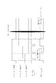
- FIG. 42 shows a specific configuration example from the both edge detection circuits 71 of the rotation / stop detection circuit 70 shown in FIG. 13 to the timer ICs (timekeeping circuits) 73 and 74.
- the resistor R11 and the capacitor C15 delay the rise of the output signal of the Hall ICH1 according to the time constant and input it to the non-inverting input terminal of the comparator 162.
- the output signal of the Hall ICH1 becomes low level, the electric charge of the capacitor C5 is discharged through the resistor R11.
- the voltage at the non-inverting input terminal of the comparator 162 is delayed from the falling edge of the output signal of the Hall ICH1 according to the time constant to a low level.
- a voltage obtained by dividing 5V by resistors R14 and R15 is input to the inverting input terminal of the comparator 162.
- the output signal of the comparator 162 rises with a delay of a predetermined time from the rise of the output signal of the hall ICH1, and falls with a delay of a predetermined time from the fall of the output signal of the hall ICH1.
- the output signal of the comparator 162 is input to one input terminal of the XOR gate 168.
- the output signal of the hall ICH1 is input to the other input terminal of the XOR gate 168.
- the output signal of the XOR gate 168 becomes a high level for a predetermined time from the rise and fall of the output signal of the hall ICH1.
- Similar processing is performed by the resistor R12, the capacitor C6, the comparator 163, and the XOR gate 169 for the output signal of the Hall ICH2, and the resistor R13, the capacitor C7, the comparator 164, and the XOR for the output signal of the Hall ICH3.
- This is done by the gate 170. That is, the output signal of the XOR gate 169 becomes a high level for a predetermined time from the rise and fall of the output signal of the hall ICH2, respectively.
- the output signal of the XOR gate 170 becomes a high level for a predetermined time from the rise and fall of the output signal of the hall ICH3, respectively.
- the output signals of the XOR gates 168 to 170 are input to the three input terminals of the OR gate 171.
- the output signal of the OR gate 171 becomes a high level for a predetermined time from the rise and fall of each output signal of the halls ICH1 to H3.
- the output signals of the XOR gates 168 to 170 are output to the I terminal, the J terminal, and the K terminal, respectively.
- the output signals of the comparators 162 to 164 are output to the C terminal, the E terminal, and the G terminal, respectively, and the level is inverted by the inverters 165 to 167 and output to the D terminal, the F terminal, and the H terminal, respectively.
- the output signal of the OR gate 171 is input to the CLK terminal of the D flip-flop 172.
- the D terminal of the D flip-flop 172 is connected to the inverted Q terminal. Every time the output signal of the OR gate 171 rises, that is, every time the edge of the output signals of the halls ICH1 to H3 appears, the high level and low level relationships of the Q terminal and the inverted Q terminal of the D flip-flop 172 are switched.
- the signal of the Q terminal of the D flip-flop 172 is input to one input terminal of the AND gate 175.
- the resistor R16 and the capacitor C8 delay the rising edge of the signal at the Q terminal of the D flip-flop 172 according to the time constant, and input the signal to the non-inverting input terminal of the comparator 173.
- the signal at the Q terminal of the D flip-flop 172 changes from high level to low level
- the electric charge of the capacitor C8 is discharged via the diode D3 and the resistor R17.
- the resistor R17 By setting the resistor R17 to a very small resistor (R17 ⁇ R16), the charge of the capacitor C8 can be rapidly consumed, and the input to the non-inverting input terminal of the comparator 173 can be instantly set to 0V. With this configuration, it is possible to keep the rising delay constant even when the signal at the Q terminal of the D flip-flop 172 is switched quickly. As a result, the voltage at the non-inverting input terminal of the comparator 173 becomes low level.
- a voltage obtained by dividing 5V by resistors R18 and R19 is input to the inverting input terminal of the comparator 173.
- the output signal of the comparator 173 rises with a predetermined time delay from the rise of the signal at the Q terminal of the D flip-flop 172.
- the output signal of the comparator 173 is level-inverted by the inverter 174 and input to the other input terminal of the AND gate 175.
- the output signal of the AND gate 175 becomes a high level only from the rise of the signal of the Q terminal of the D flip-flop 172 to the rise of the output signal of the comparator 173.
- the output signal of the AND gate 175 is input to one of the input terminals of the AND gate 176.
- the output signal of the OR gate 171 is input to the other input terminal of the AND gate 176.
- the output signal of the AND gate 176 is from the rise of the signal of the Q terminal of the D flip-flop 172 to the rise of the output signal of the comparator 173, and a predetermined time from the rise and fall of each output signal of the halls ICH1 to H3. Only during the period, it becomes a high level.
- the output signal of the AND gate 176 is output to the L terminal.
- the timer IC 183 outputs a high-level pulse to the OUT terminal for a predetermined time, triggered by the falling edge of the input signal to the TRIG terminal.
- the predetermined time is set by the resistance value of the resistor R26 connected to the VOO terminal of the timer IC183 and the capacitance value of the capacitor C10.
- the output signal of the AND gate 176 is input to the TRIG terminal of the timer IC 183 with the level inverted by the inverter 177.
- the output signal of the inverter 177 is output to the M terminal.
- the timer IC 183 outputs a pulse to the OUT terminal when the output signal of the AND gate 176 rises.
- the signal from the OUT terminal of the timer IC 183 is output to the Q terminal, and the level is inverted by the inverter 185 and output to the R terminal.
- the RST terminal of the timer IC 183 is connected to the P terminal and is connected to the 5V line via the resistor R24.
- the OUT terminal of the timer IC 183 is connected to the 5V line via the resistor R25.
- the resistors R20 to R23, the capacitor D4, the capacitor C9, the comparator 178, the inverter 179, the AND gate 180, 181 and the inverter 182, the resistors R27 to R29, the capacitor C11, the timer IC184, and the inverter 186 are D3, capacitor C8, comparator 173, inverter 174, AND gate 175, 176, inverter 177, resistors R24 to R26, capacitor C10, timer IC183, inverter 185 are the same connections, respectively, and the edges of the output signals of Hall ICH1 to H3. It works in the same way alternately every time.
- FIG. 43 shows a specific configuration example of the rotation / stop detection circuit 70 shown in FIG. 13 from the comparison circuit 75 to the rotation state storage circuit 79, and the stop detection circuit 80, the counter reset circuit 81, and the rotation state reset circuit 82. ..
- the circuit enclosed by reference numeral 76a belongs to the rotation detection circuit 76
- the circuit enclosed by reference numerals 80a and 80b and the NAND gate 206 belong to the stop detection circuit 80
- the RS flip-flops 188,195,198,205 rotate. It belongs to the detection circuit 76 and the stop detection circuit 80.
- a signal from the OUT terminal of the timer IC 184 (voltage at the T terminal) and an output signal from the AND gate 176 (voltage from the L terminal) are input to the AND gate 187.
- the AND gate 187 outputs a high level signal when both the signal of the OUT terminal of the timer IC 184 and the output signal of the AND gate 176 are high level. That is, in the AND gate 187, the next edge comes while the timer IC 184 outputs a pulse for a predetermined time to the OUT terminal by any edge of the hall ICH1 to H3, and the output signal of the AND gate 176 becomes a high level.
- a high-level signal is output while it is set to, and a low-level signal is output during the rest of the time.
- the output signal of the AND gate 187 is input to the S terminal of the RS flip-flop 188.
- the signal of the Q terminal of the RS flip-flop 188 is level-inverted by the inverter 189 and output to the S terminal.
- the output signal of the AND gate 187 rises, the signal of the Q terminal of the RS flip-flop 188 rises, and the voltage of the RST terminal of the timer IC 184 falls via the S terminal.
- the time measurement by the timer IC 184 is reset (the pulse at the OUT terminal is stopped).
- the level-inverted signal of the Q terminal of the RS flip-flop 188, the signal of the OUT terminal of the timer IC 184 (the voltage of the U terminal), and the output signal of the AND gate 176 are level-inverted.
- the signal (voltage of M terminal) and the voltage of Q terminal of RS flip-flop 195 are input and they are all high level, a high level signal is output to R terminal of RS flip-flop 188 and RS flip-flop
- the signal of the Q terminal of the flip-flop 188 is dropped (reset) to a low level.
- the signal of the Q terminal of the RS flip-flop 188 When the signal of the Q terminal of the RS flip-flop 188 is high level, the signal of the inverted Q terminal is low level, the output signal of the AND gate 194 is high level, and the signal of the Q terminal of RS flip-flop 195 is high level. Is. At this time, when the pulse of the OUT terminal of the timer IC 184 is stopped (the voltage of the U terminal becomes a high level) and the edge detection is completed (the voltage of the M terminal becomes a high level), the output signal of the AND gate 190 becomes a high level. Become. As a result, the signal at the Q terminal of the RS flip-flop 188 becomes low level, and the input signal to the R terminal of the RS flip-flop 188 becomes low level. Further, the signal of the inverted Q terminal of the RS flip-flop 188 becomes a high level.
- the next edge does not come while the timer IC 184 outputs a pulse for a predetermined time to the OUT terminal due to any edge of Hall ICH1 to H3.
- the output signal of the AND gate 176 does not reach the high level, the voltage of the S terminal of the RS flip-flop 188 remains at the low level, and the signal of the inverted Q terminal of the RS flip-flop 188 keeps the high level.
- the D flip-flop 191 has a signal (high level) of the inverted Q terminal of the RS flip-flop 188 input to its own D terminal due to the stop of the pulse of the OUT terminal of the timer IC 184 (rising edge of the voltage of the U terminal). ) Is output from its own Q terminal.
- the output signal of the AND gate 192 (input signal to the R terminal of the RS flip-flop 195) becomes high level
- the signal of the Q terminal of the RS flip-flop 195 input signal to one input terminal of the NAND gate 206) becomes high level. Fall to low level (reset).
- the signal of the inverted Q terminal of the RS flip-flop 188 and the signal of the Q terminal of the D flip-flop 191 are input to the AND gate 192, and when both of them are at a high level, a high level signal is output. ..
- the output signal of the AND gate 192 is input to the R terminal of the RS flip-flop 195, and the level is inverted by the inverter 193 and input to one input terminal of the AND gate 194.
- the signal of the Q terminal of the RS flip-flop 188 is input to the other input terminal of the AND gate 194.
- RS flip-flop 198, inverter 199, AND gate 200, D flip-flop 201, AND gate 202, inverter 203, AND gate 204, RS flip-flop 205 are the RS flip-flop 188, inverter 189, AND gate 190, D described above.
- the flip-flop 191 and the AND gate 192, the inverter 193, the AND gate 194, and the RS flip-flop 195 are connected in the same manner, and operate alternately every time the edges of the output signals of the halls ICH1 to H3 appear.
- the signal of the Q terminal of the RS flip-flop 188 and the signal of the Q terminal of the RS flip-flop 198 are input to the OR gate 196. These signals alternately become high levels each time the next edge of the output signals of Hall ICH1 to H3 appears while the timer ICs 183 and 184 are outputting pulses to the OUT terminals (during the measurement time). Therefore, the output signal of the OR gate 196 is from low level to high every time the edge appears when the motor 6 is rotating at a rotation speed equal to or higher than the rotation speed at which the edges of the halls ICH1 to H3 appear within the measurement time by the timers IC183 and 184. Transition to the level.
- the rotation counter circuit 77 counts the rising edge of the output signal of the OR gate 196.
- the output signal of the OR gate 196 is input to the CLK terminals of the D flip-flops 207 and 208.
- the signals of the Q terminals of the D flip-flops 207 and 208 are input to one and the other input terminals of the AND gate 211 and one and the other input terminals of the XOR gate 209.
- the signals of the inverted Q terminals of the D flip-flops 207 and 208 are input to one and the other input terminals of the AND gate 210.
- the D terminal and the inverted Q terminal of the D flip-flop 207 are connected to each other.
- the output terminal of the AND gate 210 is connected to the X terminal.
- the signal of the Q terminal of the D flip-flop 207 rises, and the signal of the Q terminal of the D flip-flop 208 remains at a low level.
- the signal of the Q terminal of the D flip-flop 207 transitions to a low level, and the signal of the Q terminal of the D flip-flop 208 rises.
- the signal of the Q terminal of the D flip-flop 207 rises, and the signal of the Q terminal of the D flip-flop 208 remains at a high level.
- the output signal of the AND gate 211 rises.
- the output signal of the AND gate 211 is output to the Y terminal and input to the S terminal of the RS flip-flop 214.
- the output signal of the AND gate 213 is input to the R terminal of the RS flip-flop 214.
- a signal obtained by inverting the level of the output signal of the AND gate 211 by the inverter 212 is input to one input terminal of the AND gate 213.
- the output signal of the NAND gate 206 is input to the other input terminal of the AND gate 213.
- the signal of the Q terminal of the RS flip-flop 195 and the signal of the Q terminal of the RS flip-flop 205 are input to the NAND gate 206. These signals drop to a low level when the next edge of the output signals of Hall ICH1 to H3 does not appear while the timer ICs 183 and 184 are outputting pulses to the OUT terminals (during the measurement time). As a result, the output signal of the NAND gate 206 rises.
- the output signal of the NAND gate 206 is input to one input terminal of the three-input OR gate 215. Signals from the V terminal and the W terminal are input to the other two input terminals of the OR gate 215. As will be described later, the signals of the V terminal and the W terminal are signals that temporarily reach a high level only when the rotation direction of the motor 6 is switched, as will be described later. Therefore, when the rotation direction is not switched, the output signal of the OR gate 215 also rises when the output signal of the NAND gate 206 rises.
- the output signal of the NAND gate 206 is input to the CLR terminals of the D flip-flops 207 and 208.
- the output signal of the OR gate 215 rises, the signals of the Q terminals of the D flip-flops 207 and 208 are cleared to a low level (the count value by the rotation counter circuit 77 is cleared and becomes 0).
- the count value by the rotation counter circuit 77 even when the right rotation and the left rotation are repeated at high speed by hand rotation or the like at the position where the rising or falling edges of the halls ICH1 to H3 are detected. Is reset and rotation detection can not be generated. That is, there is an effect that erroneous detection due to manual rotation or the like can be prevented.
- the output signal of the NAND gate 206 is input to the other input terminal of the AND gate 213.
- the signal to one input terminal of the AND gate 213 becomes high level. Therefore, when the output signal of the NAND gate 206 rises, the output signal of the AND gate 213 rises.
- the signal at the Q terminal of the RS flip-flop 214 is reset to the low level, and the state shifts from the rotating state to the stopped state.
- the output signal of the NAND gate 206 is output to the B terminal.
- FIG. 44 is a circuit diagram showing a specific configuration example of the edge direction detection circuit 92a, the Hall IC comparison selection circuit 94a, and the rotation direction detection circuit (undetermined) 95a shown in FIG.
- the AND gate 216 outputs a signal of the logical product of the output signal of the hall ICH2 and the signal of the D terminal.
- the AND gate 217 outputs a signal of the logical product of the output signal of the hall ICH3 and the signal of the C terminal.
- the OR gate 218 outputs a signal of the logical sum of the output signals of the AND gates 216 and 217.
- the AND gate 219 outputs a signal of the logical product of the output signal of the hall ICH3 and the signal of the D terminal.
- the AND gate 220 outputs a signal of the logical product of the output signal of the hall ICH2 and the signal of the C terminal.
- the OR gate 221 outputs a signal of the logical sum of the output signals of the AND gates 219 and 220.
- the signal of the AA terminal is a high level when the set rotation direction of the motor 6 (hereinafter, “set rotation direction”) is left rotation, and a low level when the motor 6 is rotating clockwise.
- the AND gate 223 outputs a signal of the logical product of the signal whose level is inverted by the inverter 222 and the output signal of the OR gate 218.
- the AND gate 225 outputs a signal of the logical product of the signal of the AA terminal and the output signal of the OR gate 221.
- the OR gate 224 outputs a signal obtained by summing the output signals of the AND gates 223 and 225.
- the output signal of the OR gate 224 is input to the D terminal of the D flip-flop 226.
- the signal of the I terminal is input to the CLK terminal of the D flip-flop 226.
- the D flip-flop 226 outputs the input signal to its own D terminal to its own Q terminal, reverses the level, and reverses its own Q. Output to the terminal.
- the level of the signal at the D terminal of the D flip-flop 226 at the rising timing of the signal at the I terminal differs depending on whether or not the set rotation direction coincides with the actual rotation direction of the motor 6 (hereinafter, “actual rotation direction”).
- the signal of the D terminal of the D flip-flop 226 is input by the OR gate 224, and the OR gate 224 is input by the AND gates 223 and 225.
- the AND gates 223 and 225 each input a level inversion signal in the set rotation direction, and only one of them has a high level and the other has a low level at all times.
- the signal of C terminal is low level
- the signal of D terminal is high level
- the output signal of Hall ICH2 is low level and Hall ICH3.
- the output signal is high level.
- the input from the OR gate 218 is output as it is to the OR gate 224 from the above. Since the output signal of the AND gate 216 is low level and the signal of the AND gate 217 is low level, the output signals of the OR gate 218 and the OR gate 224 (the signal of the D terminal of the D flip-flop 226) are low level.
- the OR gate 224 outputs the input from the OR gate 221 as it is. Since the output signal of the AND gate 219 is high level and the signal of the AND gate 220 is high level, the output signal of the OR gate 224 (the signal of the D terminal of the D flip-flop 226) is high level.
- the signal of C terminal is high level
- the signal of D terminal is low level
- the output signal of Hall ICH2 is high level and Hall ICH3.
- Output signal is low level.
- the set rotation direction is clockwise rotation (low level signal)
- the input from the OR gate 218 is output as it is to the OR gate 224 from the above. Since the output signal of the AND gate 216 is low level and the signal of the AND gate 217 is low level, the output signal of the OR gate 224 (the signal of the D terminal of the D flip-flop 226) is low level.
- the OR gate 224 outputs the input from the OR gate 221 as it is. Since the output signal of the AND gate 219 is high level and the signal of the AND gate 220 is high level, the output signal of the OR gate 224 (the signal of the D terminal of the D flip-flop 226) is high level.
- the output signal of the OR gate 224 (the signal of the D terminal of the D flip-flop 226) has the actual rotation direction one with the set rotation direction at the edge timing of the output signal of the hall ICH1 even when the actual rotation direction is left rotation. If it is done, it is low level, and if the actual rotation direction does not match the set rotation direction, it is high level.
- the signal of the Q terminal of the D flip-flop 226 is output to the DD terminal and input to the Hall IC1 reference inversion detection circuit 228.
- the circuit set consisting of resistors R30 to R33, diode D5, capacitor C12, comparator 230, inverter 231 and AND gate 232 is an AND gate when the signal of the Q terminal of the D flip-flop 226 rises. A signal that becomes high level for a predetermined time is output from 232.
- the signal of the inverted Q terminal of the D flip-flop 226 is input to the Hall IC1 reference normal rotation detection circuit 229.
- the circuit set consisting of resistors R40 to R43, diode D6, capacitor C13, comparator 235, inverter 236, and AND gate 237 is used when the signal of the inverted Q terminal of the D flip-flop 226 rises.
- a signal that becomes high level for a predetermined time is output from the AND gate 237.
- the AND gate 234 outputs a signal of the logical product of the output signal of the AND gate 232 and the signal whose level is inverted by the inverter 233 of the output signal of the AND gate 237 to the EE terminal.
- the AND gate 239 outputs a signal of the logical product of the output signal of the AND gate 237 and the signal whose level is inverted by the inverter 238 of the output signal of the AND gate 232 to the FF terminal.
- the circuit of FIG. 45 has a reference signal changed to the output signal of Hall ICH2, and has the same circuit configuration. Further, in the circuit of FIG. 46, the reference signal is changed to the output signal of the hall ICH3 as compared with FIG. 44, and the circuit configuration is the same.
- FIG. 47 is a circuit diagram showing specific configuration examples of the rotation direction change detection circuits 96a to 96c, the rotation direction determination circuit 97, the rotation direction reset circuit 98, and the rotation direction storage circuit 99 shown in FIG.
- the OR gate 270 outputs a signal of the logical sum of the signals of the EE terminal, the HH terminal, and the KK terminal.
- the AND gate 271 outputs a signal of the logical product of the signals of the DD terminal, the GG terminal, and the JJ terminal.
- the AND gate 272 outputs a signal of the logical product of the output signal of the OR gate 270 and the output signal of the AND gate 271 to the V terminal and the AND gate 273.
- the AND gate 273 outputs a signal of the logical product of the signals of the XX terminal, the X terminal, and the output terminal of the AND gate 272 to the BB terminal.
- the signal at the V terminal indicates that the actual rotation direction and the set rotation direction have been switched from coincident to disagreeable by the high-level pulse signal, and a pulse is output at that time. For example, when the signals of Hall ICH2 and Hall ICH3 are used as the reference, the rotation is normal, but when the signals of Hall ICH1 are used, the rotation is reversed.
- the OR gate 274 outputs a signal of the logical sum of the signals of the FF terminal, the II terminal, and the LL terminal.
- the OR gate 275 outputs a signal of the logical sum of the signals of the DD terminal, the GG terminal, and the JJ terminal.
- the AND gate 276 outputs a signal of the logical product of the output signals of the OR gates 274 and 275 to the W terminal and the AND gate 277.
- the AND gate 277 outputs a signal of the logical product of the signals of the MM terminal, the X terminal, and the output terminal of the AND gate 276 to the CC terminal.
- the signal of the W terminal indicates that the actual rotation direction and the set rotation direction have been switched from the mismatch to the match, and a pulse is output at that time. For example, it was reversed when the signals of Hall ICH2 and Hall ICH3 were used as a reference, but it was reversed when the signal of Hall ICH1 was used as the reference.
- the OR gate 278 outputs a signal of the logical sum of the signal of the W terminal and the signal of the B terminal.
- the output signal of the OR gate 278 (input signal to the R terminal of the RS flip-flop) was detected when the stop of the motor 6 was detected, or the actual rotation direction and the set rotation direction were switched from mismatch to match. In this case, the level becomes high and the Q terminal signal of the RS flip-flop 281 is reset to the low level.
- the AND gate 280 outputs a signal of the logical product of the signal of the V terminal and the signal of the level inversion of the output signal of the OR gate 278 by the inverter 279 to the S terminal of the RS flip-flop 281.
- the output signal of the AND gate 280 (input signal to the S terminal of the RS flip-flop) is a case where it is detected that the actual rotation direction and the set rotation direction are switched from the match to the mismatch, and the stop of the motor 6 is detected.
- the high level is set when the actual rotation direction and the set rotation direction are not detected and it is not detected that the rotation direction is switched from the mismatch to the match.
- the signal of the Q terminal of the RS flip-flop 281 is output to the XX terminal, and the signal of the inverted Q terminal is output to the MM terminal.
- the rotation state detection circuit 282 receives the signal of the Y terminal as an input, and outputs a signal that starts up with a delay of a predetermined time from the timing when the count value of the rotation counter circuit 77 reaches 3.
- the AND gate 283 outputs a signal of the logical product of the signal of the inverted Q terminal of the RS flip-flop 281 and the output signal of the rotation state detection circuit 282.
- the OR gate 286 outputs a signal of the logical sum of the output signal of the AND gate 283 and the signal of the B terminal to the R terminal of the RS flip-flop 287.
- the AND gate 285 provides a signal of the logical product of the signal of the Q terminal of the RS flip-flop 281, the output signal of the rotation state detection circuit 282, and the signal of the level of the output signal of the OR gate 286 inverted by the inverter 284. It is output to the S terminal of the RS flip-flop 287 as a rotation direction detection signal.
- the signal of the Q terminal of the RS flip-flop 287 is output to the NN terminal.
- the signal at the NN terminal is low level when the rotation direction is forward rotation, and high level when the rotation direction is reverse rotation.
- FIG. 48 shows a specific configuration example of the trigger ON stop detection circuit 100 shown in FIG. 24 and the trigger OFF rotation detection circuit 120 shown in FIG. 28.
- the trigger switch 5 When the trigger switch 5 is pulled (operated), a low-level signal is output to the OO terminal and a high-level signal is output to the WW terminal.
- the trigger switch 5 When the trigger switch 5 is released (not operated), a high-level signal is output to the OO terminal and a low-level signal is output to the WW terminal.
- the double-edge detection circuit (for trigger) 290 is a signal (short pulse) that becomes a high level for a predetermined time when a change in the state of the trigger switch 5 (change from an operating state to a non-operating state, or vice versa) occurs. ) Is output from the XOR gate 292.
- the output signal of the comparator 291 undergoes a level transition with a delay of a predetermined time from the level transition of the signal at the OO terminal. Therefore, the output signal of the comparator 291 is at a low level at the timing of the rising edge of the signal of the OO terminal, and the output signal of the comparator 291 is at a high level at the timing of the falling edge. Therefore, the output signal of the comparator 291 can be used for detecting the edge direction of the output signal of the OO terminal.
- the AND gate 294 outputs a signal of the logical product of the output signal of the XOR gate 292 and the signal whose level of the output signal of the comparator 291 is inverted by the inverter 293.
- the output signal of the AND gate 294 rises at the timing of the rising edge of the signal of the OO terminal.
- the output signal of the AND gate 294 is output to the RR terminal.
- the AND gate 295 outputs a signal of the logical product of the output signal of the XOR gate 292 and the output signal of the comparator 291.
- the output signal of the AND gate 295 rises at the timing of the falling edge of the signal of the OO terminal.
- the output signal of the AND gate 295 is output to the QQ terminal.
- the output signal of the AND gate 295 is input to the CLK terminal of the D flip-flop 297.
- a signal obtained by inverting the level of the Z terminal signal by the inverter 296 is input to the D terminal of the D flip-flop 297.
- the D flip-flop 297 outputs a low-level signal to the Q terminal and outputs a high-level signal to the inverted Q terminal if the rotation of the motor 6 is detected at the timing when the trigger switch 5 is pulled.
- the D flip-flop 297 outputs a high-level signal to the Q terminal and outputs a low-level signal to the inverted Q terminal if the rotation of the motor 6 is not detected at the timing when the trigger switch 5 is pulled.
- the output signal of the AND gate 295 is input to the CLK terminal of the D flip-flop 298.
- the signal of the Z terminal is input to the D terminal of the D flip-flop 298.
- the D flip-flop 298 outputs a high-level signal to the Q terminal if the rotation of the motor 6 is detected at the timing when the trigger switch 5 is pulled.
- the D flip-flop 298 outputs a low-level signal to the Q terminal if the rotation of the motor 6 is not detected at the timing when the trigger switch 5 is pulled.
- the AND gate 299 outputs a signal of the logical product of the signal of the UU terminal, the signal of the WW terminal, the signal of the B terminal, and the signal of the Q terminal of the D flip-flop 298.
- the AND gate 299 detects that the motor 6 is stopped outside the measurement time by the timer IC 307 while the trigger switch 5 is pulled. In other cases, a high-level signal is output, and in other cases, a low-level signal is output.
- the AND gate 301 outputs a signal of the logical product of the signal of the RR terminal and the signal whose level of the output signal of the AND gate 299 is inverted by the inverter 300.
- the output signal of the AND gate 299 is input to the S terminal, and the output signal of the AND gate 301 is input to the R terminal.
- the OR gate 303 outputs a signal of the logical sum of the signal of the Q terminal of the D flip-flop 297 and the signal of the Q terminal of the RS flip-flop 302.
- the AND gate 305 is a signal having a logical product of the output signal of the OR gate 303 and the level inversion signal of the signal obtained by delaying the output signal by a predetermined time, that is, a predetermined time from the rising timing of the output signal of the OR gate 303. Only high level signal (short pulse) is output. The output signal of the comparator 304 is output to the SS terminal.
- a signal obtained by inverting the level of the output signal of the AND gate 305 by the inverter 306 is input to the TRIG terminal of the timer IC 307.
- the timer IC 307 outputs a high-level pulse for a predetermined time to the OUT terminal, triggered by the falling edge of the input signal to the TRIG terminal.
- the signal at the OUT terminal of the timer IC 307 is level-inverted by the inverter 309 and output to the UU terminal.
- a signal whose level is inverted by the inverter 308 is input to the RST terminal of the timer IC 307.
- the AND gate 319 outputs a signal of the logical product of the signal of the SS terminal, the signal of the WW terminal, the signal of the UU terminal, and the signal of the B terminal.
- the AND gate 321 outputs a signal of the logical product of the signal whose level is inverted by the inverter 320 and the signal of the RR terminal.
- the output signal of the AND gate 319 is input to the S terminal, and the output signal of the AND gate 321 is input to the R terminal.
- the signal of the Q terminal of the RS flip-flop 322 is output to the VV terminal.
- the signal of the VV terminal becomes a high level when the motor 6 is stopped even after the measurement time of the timer IC 307 has passed in the state where the trigger switch 5 is pulled, and becomes a low level in other cases.
- a signal obtained by inverting the level of the output signal of the AND gate 294 by the inverter 310 is input to the TRIG terminal of the timer IC 312.
- the timer IC 312 outputs a high-level pulse for a predetermined time to the OUT terminal, triggered by the falling edge of the input signal to the TRIG terminal.
- a signal whose level is inverted by the inverter 312 is input to the RST terminal of the timer IC 312.
- the AND gate 313 outputs a signal of the logical product of the signal of the OO terminal and the signal of the PP terminal.
- the AND gate 135 outputs a signal of the logical product of the output signal of the AND gate 313, the signal of the OUT terminal of the timer IC 312 whose level is inverted by the inverter 314, and the signal of the Z terminal.
- the AND gate 317 outputs a signal of the logical product of the signal whose level is inverted by the inverter 316 and the signal of the B terminal.
- the output signal of the AND gate 315 is input to the S terminal
- the output signal of the AND gate 317 is input to the R terminal.
- the signal of the Q terminal of the RS flip-flop 318 is output to the TT terminal.
- the signal of the TT terminal becomes a high level when the rotation of the motor 6 is detected even after the measurement time of the timer IC 312 has passed in a state where the hand is away from the trigger switch 5, and becomes a low level in other cases. ..
- FIG. 49 shows a specific configuration example of the abnormal state integrated storage circuit 131 and the abnormal state integrated reset circuit 132 shown in FIG.
- the OR gate 331 outputs a signal of the logical sum of the signal of the A terminal, the signal of the NN terminal, the signal of the TT terminal, and the signal of the VV terminal.
- the AND gate 333 outputs a signal of the logical product of the signal whose level is inverted by the inverter 332 and the signal of the OO terminal.
- the output signal of the OR gate 331 is input to the S terminal, and the output signal of the AND gate 333 is input to the R terminal.
- the signal at the Q terminal of the RS flip-flop 334 is an integrated error signal.
- the integrated error signal is high level when at least one of over-rotation abnormality, rotation direction abnormality, unintended stop, and unintended rotation is detected, and low level in other cases.
- the second control unit 50 is not limited to detecting all of the over-rotation, reverse rotation, unintended stop, and unintended rotation of the motor 6, and may be configured to detect only a part of the motor 6.
- a sensorless method for detecting the position of the rotor core 6b by extracting the induced electromotive force (back electromotive force) of the stator coil 6e as a logical signal through the filter unit without providing a sensor such as a hall IC42 as a rotation position detection unit. May be good.
- the first control unit and the second control unit may function as the rotation position detection unit, or the filter unit may function as the rotation position detection unit.
- FIG. 50 is a left side view of the electric work machine 1A in which the first control unit 40 is mounted on the first control board 41a and the second control unit 50 is mounted on the second control board 41b with respect to a modified example.
- the first control board 41a has the same arrangement as the control board 41 of the embodiment.
- the second control board 41b is provided in the handle housing 12 at a position on the right side of the battery pack 51 so as to be perpendicular to the left-right direction.
- the first control board 41a and the second control board 41b are electrically connected to each other by wiring 41c.
- the wiring 41c is from the first control board 41a to the second control board 41b from each signal line for transmitting the output signals of Hall ICH1 to H3, the output signal of the trigger switch 5, the error signal, and the like, and the first control board 41a. Includes a power supply line to the second control board 41b.
- the electric working machine 1A can be configured to be capable of normal operation without mounting the second control board 41b. It is also possible to select that the second control board 41b is mounted with a tool (for example, a circular saw) that needs to suppress malfunction more, and is not mounted with a tool (for example, an impact driver) that does not.
- LED drive circuit 40 ... 1st control unit, 41 ... control board, 42 ... Hall IC (rotational position detection element), 43 ... inverter circuit (2nd cutoff unit), 50 ... 2nd control unit, 51 ... battery pack , Rs ... Detection resistance
Landscapes
- Engineering & Computer Science (AREA)
- Power Engineering (AREA)
- Mechanical Engineering (AREA)
- Control Of Motors That Do Not Use Commutators (AREA)
Priority Applications (1)
| Application Number | Priority Date | Filing Date | Title |
|---|---|---|---|
| JP2021556196A JPWO2021095880A1 (https=) | 2019-11-15 | 2020-11-13 |
Applications Claiming Priority (2)
| Application Number | Priority Date | Filing Date | Title |
|---|---|---|---|
| JP2019206656 | 2019-11-15 | ||
| JP2019-206656 | 2019-11-15 |
Publications (1)
| Publication Number | Publication Date |
|---|---|
| WO2021095880A1 true WO2021095880A1 (ja) | 2021-05-20 |
Family
ID=75912394
Family Applications (1)
| Application Number | Title | Priority Date | Filing Date |
|---|---|---|---|
| PCT/JP2020/042522 Ceased WO2021095880A1 (ja) | 2019-11-15 | 2020-11-13 | 電気機器 |
Country Status (2)
| Country | Link |
|---|---|
| JP (1) | JPWO2021095880A1 (https=) |
| WO (1) | WO2021095880A1 (https=) |
Cited By (2)
| Publication number | Priority date | Publication date | Assignee | Title |
|---|---|---|---|---|
| US20220404422A1 (en) * | 2021-06-17 | 2022-12-22 | Denso Corporation | Actuator control device |
| WO2024150732A1 (ja) | 2023-01-10 | 2024-07-18 | 日本製鉄株式会社 | 無方向性電磁鋼板 |
Citations (2)
| Publication number | Priority date | Publication date | Assignee | Title |
|---|---|---|---|---|
| JP2007106180A (ja) * | 2005-10-11 | 2007-04-26 | Nsk Ltd | 電動式ステアリング装置 |
| JP2012120338A (ja) * | 2010-12-01 | 2012-06-21 | Sharp Corp | モータの回転制御装置及び方法、並びにそれを用いた画像形成装置 |
Family Cites Families (2)
| Publication number | Priority date | Publication date | Assignee | Title |
|---|---|---|---|---|
| JPH0731175A (ja) * | 1993-07-15 | 1995-01-31 | Nippon Seiko Kk | Pll制御方式回転制御装置 |
| JP2019168030A (ja) * | 2018-03-23 | 2019-10-03 | 株式会社デンソー | シフトレンジ制御装置 |
-
2020
- 2020-11-13 JP JP2021556196A patent/JPWO2021095880A1/ja active Pending
- 2020-11-13 WO PCT/JP2020/042522 patent/WO2021095880A1/ja not_active Ceased
Patent Citations (2)
| Publication number | Priority date | Publication date | Assignee | Title |
|---|---|---|---|---|
| JP2007106180A (ja) * | 2005-10-11 | 2007-04-26 | Nsk Ltd | 電動式ステアリング装置 |
| JP2012120338A (ja) * | 2010-12-01 | 2012-06-21 | Sharp Corp | モータの回転制御装置及び方法、並びにそれを用いた画像形成装置 |
Cited By (5)
| Publication number | Priority date | Publication date | Assignee | Title |
|---|---|---|---|---|
| US20220404422A1 (en) * | 2021-06-17 | 2022-12-22 | Denso Corporation | Actuator control device |
| US11982717B2 (en) * | 2021-06-17 | 2024-05-14 | Denso Corporation | Actuator control device |
| WO2024150732A1 (ja) | 2023-01-10 | 2024-07-18 | 日本製鉄株式会社 | 無方向性電磁鋼板 |
| KR20250133748A (ko) | 2023-01-10 | 2025-09-08 | 닛폰세이테츠 가부시키가이샤 | 무방향성 전자 강판 |
| EP4650475A1 (en) | 2023-01-10 | 2025-11-19 | Nippon Steel Corporation | Non-oriented electromagnetic steel sheet |
Also Published As
| Publication number | Publication date |
|---|---|
| JPWO2021095880A1 (https=) | 2021-05-20 |
Similar Documents
| Publication | Publication Date | Title |
|---|---|---|
| CN107371563B (zh) | 作业机 | |
| US9853586B2 (en) | Motor driven appliance | |
| JP5755988B2 (ja) | 電動工具 | |
| CN107685315B (zh) | 电动工具 | |
| US8324845B2 (en) | Rechargeable power tool, control unit and recording medium | |
| JP6701533B2 (ja) | 電動工具 | |
| EP2969397B1 (en) | Power tool operation recording and playback | |
| JP6252778B2 (ja) | 電動工具 | |
| JP5408416B2 (ja) | 電動工具 | |
| JP5983928B2 (ja) | 電動作業機 | |
| WO2021095880A1 (ja) | 電気機器 | |
| JP6753472B2 (ja) | 電動工具 | |
| JP7047462B2 (ja) | 電動工具 | |
| JP7816859B2 (ja) | 設定可能なモーター固定子巻線を含む電動工具 | |
| CN112491327A (zh) | 电动作业机 | |
| JP2015147261A (ja) | 電動機械器具 | |
| JPWO2017094414A1 (ja) | 電動工具 | |
| US12042951B2 (en) | Electric work machine | |
| JP2017205834A (ja) | 電動作業機 | |
| JP7406927B2 (ja) | 電動作業機 | |
| JP2013188825A (ja) | 電動工具 | |
| JP4127201B2 (ja) | 電動工具 | |
| JP2013188821A (ja) | 電動工具 | |
| JP2019033649A (ja) | 電動工具 | |
| JP6675259B2 (ja) | 電動作業機 |
Legal Events
| Date | Code | Title | Description |
|---|---|---|---|
| 121 | Ep: the epo has been informed by wipo that ep was designated in this application |
Ref document number: 20888349 Country of ref document: EP Kind code of ref document: A1 |
|
| ENP | Entry into the national phase |
Ref document number: 2021556196 Country of ref document: JP Kind code of ref document: A |
|
| NENP | Non-entry into the national phase |
Ref country code: DE |
|
| 122 | Ep: pct application non-entry in european phase |
Ref document number: 20888349 Country of ref document: EP Kind code of ref document: A1 |