WO2021065948A1 - 光導波路パッケージおよび発光装置 - Google Patents
光導波路パッケージおよび発光装置 Download PDFInfo
- Publication number
- WO2021065948A1 WO2021065948A1 PCT/JP2020/037008 JP2020037008W WO2021065948A1 WO 2021065948 A1 WO2021065948 A1 WO 2021065948A1 JP 2020037008 W JP2020037008 W JP 2020037008W WO 2021065948 A1 WO2021065948 A1 WO 2021065948A1
- Authority
- WO
- WIPO (PCT)
- Prior art keywords
- light emitting
- optical waveguide
- recess
- waveguide package
- view
- Prior art date
- Legal status (The legal status is an assumption and is not a legal conclusion. Google has not performed a legal analysis and makes no representation as to the accuracy of the status listed.)
- Ceased
Links
Images


Classifications
-
- G—PHYSICS
- G02—OPTICS
- G02B—OPTICAL ELEMENTS, SYSTEMS OR APPARATUS
- G02B6/00—Light guides; Structural details of arrangements comprising light guides and other optical elements, e.g. couplings
- G02B6/10—Light guides; Structural details of arrangements comprising light guides and other optical elements, e.g. couplings of the optical waveguide type
- G02B6/12—Light guides; Structural details of arrangements comprising light guides and other optical elements, e.g. couplings of the optical waveguide type of the integrated circuit kind
-
- G—PHYSICS
- G02—OPTICS
- G02B—OPTICAL ELEMENTS, SYSTEMS OR APPARATUS
- G02B6/00—Light guides; Structural details of arrangements comprising light guides and other optical elements, e.g. couplings
- G02B6/24—Coupling light guides
- G02B6/42—Coupling light guides with opto-electronic elements
- G02B6/4201—Packages, e.g. shape, construction, internal or external details
- G02B6/4219—Mechanical fixtures for holding or positioning the elements relative to each other in the couplings; Alignment methods for the elements, e.g. measuring or observing methods especially used therefor
- G02B6/4236—Fixing or mounting methods of the aligned elements
- G02B6/424—Mounting of the optical light guide
-
- H—ELECTRICITY
- H10—SEMICONDUCTOR DEVICES; ELECTRIC SOLID-STATE DEVICES NOT OTHERWISE PROVIDED FOR
- H10H—INORGANIC LIGHT-EMITTING SEMICONDUCTOR DEVICES HAVING POTENTIAL BARRIERS
- H10H20/00—Individual inorganic light-emitting semiconductor devices having potential barriers, e.g. light-emitting diodes [LED]
- H10H20/80—Constructional details
- H10H20/85—Packages
- H10H20/855—Optical field-shaping means, e.g. lenses
-
- G—PHYSICS
- G02—OPTICS
- G02B—OPTICAL ELEMENTS, SYSTEMS OR APPARATUS
- G02B6/00—Light guides; Structural details of arrangements comprising light guides and other optical elements, e.g. couplings
- G02B6/24—Coupling light guides
- G02B6/42—Coupling light guides with opto-electronic elements
- G02B6/4201—Packages, e.g. shape, construction, internal or external details
- G02B6/4204—Packages, e.g. shape, construction, internal or external details the coupling comprising intermediate optical elements, e.g. lenses, holograms
- G02B6/4206—Optical features
-
- G—PHYSICS
- G02—OPTICS
- G02B—OPTICAL ELEMENTS, SYSTEMS OR APPARATUS
- G02B6/00—Light guides; Structural details of arrangements comprising light guides and other optical elements, e.g. couplings
- G02B6/24—Coupling light guides
- G02B6/42—Coupling light guides with opto-electronic elements
- G02B6/4201—Packages, e.g. shape, construction, internal or external details
- G02B6/4219—Mechanical fixtures for holding or positioning the elements relative to each other in the couplings; Alignment methods for the elements, e.g. measuring or observing methods especially used therefor
- G02B6/4228—Passive alignment, i.e. without a detection of the degree of coupling or the position of the elements
- G02B6/423—Passive alignment, i.e. without a detection of the degree of coupling or the position of the elements using guiding surfaces for the alignment
-
- G—PHYSICS
- G02—OPTICS
- G02B—OPTICAL ELEMENTS, SYSTEMS OR APPARATUS
- G02B6/00—Light guides; Structural details of arrangements comprising light guides and other optical elements, e.g. couplings
- G02B6/24—Coupling light guides
- G02B6/42—Coupling light guides with opto-electronic elements
- G02B6/4201—Packages, e.g. shape, construction, internal or external details
- G02B6/4219—Mechanical fixtures for holding or positioning the elements relative to each other in the couplings; Alignment methods for the elements, e.g. measuring or observing methods especially used therefor
- G02B6/4236—Fixing or mounting methods of the aligned elements
- G02B6/4244—Mounting of the optical elements
-
- G—PHYSICS
- G02—OPTICS
- G02B—OPTICAL ELEMENTS, SYSTEMS OR APPARATUS
- G02B6/00—Light guides; Structural details of arrangements comprising light guides and other optical elements, e.g. couplings
- G02B6/24—Coupling light guides
- G02B6/42—Coupling light guides with opto-electronic elements
- G02B6/4201—Packages, e.g. shape, construction, internal or external details
- G02B6/4256—Details of housings
- G02B6/4257—Details of housings having a supporting carrier or a mounting substrate or a mounting plate
-
- H—ELECTRICITY
- H01—ELECTRIC ELEMENTS
- H01S—DEVICES USING THE PROCESS OF LIGHT AMPLIFICATION BY STIMULATED EMISSION OF RADIATION [LASER] TO AMPLIFY OR GENERATE LIGHT; DEVICES USING STIMULATED EMISSION OF ELECTROMAGNETIC RADIATION IN WAVE RANGES OTHER THAN OPTICAL
- H01S5/00—Semiconductor lasers
- H01S5/005—Optical components external to the laser cavity, specially adapted therefor, e.g. for homogenisation or merging of the beams or for manipulating laser pulses, e.g. pulse shaping
- H01S5/0071—Optical components external to the laser cavity, specially adapted therefor, e.g. for homogenisation or merging of the beams or for manipulating laser pulses, e.g. pulse shaping for beam steering, e.g. using a mirror outside the cavity to change the beam direction
-
- H—ELECTRICITY
- H01—ELECTRIC ELEMENTS
- H01S—DEVICES USING THE PROCESS OF LIGHT AMPLIFICATION BY STIMULATED EMISSION OF RADIATION [LASER] TO AMPLIFY OR GENERATE LIGHT; DEVICES USING STIMULATED EMISSION OF ELECTROMAGNETIC RADIATION IN WAVE RANGES OTHER THAN OPTICAL
- H01S5/00—Semiconductor lasers
- H01S5/02—Structural details or components not essential to laser action
- H01S5/022—Mountings; Housings
- H01S5/0225—Out-coupling of light
-
- H—ELECTRICITY
- H01—ELECTRIC ELEMENTS
- H01S—DEVICES USING THE PROCESS OF LIGHT AMPLIFICATION BY STIMULATED EMISSION OF RADIATION [LASER] TO AMPLIFY OR GENERATE LIGHT; DEVICES USING STIMULATED EMISSION OF ELECTROMAGNETIC RADIATION IN WAVE RANGES OTHER THAN OPTICAL
- H01S5/00—Semiconductor lasers
- H01S5/02—Structural details or components not essential to laser action
- H01S5/022—Mountings; Housings
- H01S5/023—Mount members, e.g. sub-mount members
- H01S5/02325—Mechanically integrated components on mount members or optical micro-benches
- H01S5/02326—Arrangements for relative positioning of laser diodes and optical components, e.g. grooves in the mount to fix optical fibres or lenses
-
- H—ELECTRICITY
- H01—ELECTRIC ELEMENTS
- H01S—DEVICES USING THE PROCESS OF LIGHT AMPLIFICATION BY STIMULATED EMISSION OF RADIATION [LASER] TO AMPLIFY OR GENERATE LIGHT; DEVICES USING STIMULATED EMISSION OF ELECTROMAGNETIC RADIATION IN WAVE RANGES OTHER THAN OPTICAL
- H01S5/00—Semiconductor lasers
- H01S5/40—Arrangement of two or more semiconductor lasers, not provided for in groups H01S5/02 - H01S5/30
- H01S5/4012—Beam combining, e.g. by the use of fibres, gratings, polarisers, prisms
-
- H—ELECTRICITY
- H10—SEMICONDUCTOR DEVICES; ELECTRIC SOLID-STATE DEVICES NOT OTHERWISE PROVIDED FOR
- H10H—INORGANIC LIGHT-EMITTING SEMICONDUCTOR DEVICES HAVING POTENTIAL BARRIERS
- H10H20/00—Individual inorganic light-emitting semiconductor devices having potential barriers, e.g. light-emitting diodes [LED]
- H10H20/80—Constructional details
- H10H20/85—Packages
-
- G—PHYSICS
- G02—OPTICS
- G02B—OPTICAL ELEMENTS, SYSTEMS OR APPARATUS
- G02B6/00—Light guides; Structural details of arrangements comprising light guides and other optical elements, e.g. couplings
- G02B6/24—Coupling light guides
- G02B6/42—Coupling light guides with opto-electronic elements
- G02B6/4201—Packages, e.g. shape, construction, internal or external details
- G02B6/4204—Packages, e.g. shape, construction, internal or external details the coupling comprising intermediate optical elements, e.g. lenses, holograms
-
- G—PHYSICS
- G02—OPTICS
- G02B—OPTICAL ELEMENTS, SYSTEMS OR APPARATUS
- G02B6/00—Light guides; Structural details of arrangements comprising light guides and other optical elements, e.g. couplings
- G02B6/24—Coupling light guides
- G02B6/42—Coupling light guides with opto-electronic elements
- G02B6/4201—Packages, e.g. shape, construction, internal or external details
- G02B6/4274—Electrical aspects
- G02B6/428—Electrical aspects containing printed circuit boards [PCB]
-
- H—ELECTRICITY
- H01—ELECTRIC ELEMENTS
- H01S—DEVICES USING THE PROCESS OF LIGHT AMPLIFICATION BY STIMULATED EMISSION OF RADIATION [LASER] TO AMPLIFY OR GENERATE LIGHT; DEVICES USING STIMULATED EMISSION OF ELECTROMAGNETIC RADIATION IN WAVE RANGES OTHER THAN OPTICAL
- H01S5/00—Semiconductor lasers
- H01S5/02—Structural details or components not essential to laser action
- H01S5/022—Mountings; Housings
- H01S5/0225—Out-coupling of light
- H01S5/02253—Out-coupling of light using lenses
-
- H—ELECTRICITY
- H01—ELECTRIC ELEMENTS
- H01S—DEVICES USING THE PROCESS OF LIGHT AMPLIFICATION BY STIMULATED EMISSION OF RADIATION [LASER] TO AMPLIFY OR GENERATE LIGHT; DEVICES USING STIMULATED EMISSION OF ELECTROMAGNETIC RADIATION IN WAVE RANGES OTHER THAN OPTICAL
- H01S5/00—Semiconductor lasers
- H01S5/40—Arrangement of two or more semiconductor lasers, not provided for in groups H01S5/02 - H01S5/30
- H01S5/4025—Array arrangements, e.g. constituted by discrete laser diodes or laser bar
- H01S5/4087—Array arrangements, e.g. constituted by discrete laser diodes or laser bar emitting more than one wavelength
- H01S5/4093—Red, green and blue [RGB] generated directly by laser action or by a combination of laser action with nonlinear frequency conversion
-
- H—ELECTRICITY
- H10—SEMICONDUCTOR DEVICES; ELECTRIC SOLID-STATE DEVICES NOT OTHERWISE PROVIDED FOR
- H10W—GENERIC PACKAGES, INTERCONNECTIONS, CONNECTORS OR OTHER CONSTRUCTIONAL DETAILS OF DEVICES COVERED BY CLASS H10
- H10W90/00—Package configurations
Definitions
- the present disclosure relates to an optical waveguide package and a light emitting device.
- Patent Document 1 An example of the prior art is described in Patent Document 1.
- the optical waveguide package of the present disclosure includes a substrate having a first surface and A clad having a second surface located on the first surface and facing the first surface and a third surface located opposite to the second surface.
- the clad With a core located within the clad and extending in the first direction, The clad is open to the third surface and has a recess in which the element mounting portion is located in a plan view toward the first surface.
- the core is connected to the recess and is connected to the recess.
- the recess has a plurality of wall surfaces that intersect the third surface and corner support surfaces that are located between the adjacent wall surfaces.
- the light emitting device of the present disclosure includes the optical waveguide package and The light emitting element located in the element mounting portion and It includes a lens located on the optical path of light emitted from the core.
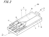
- FIG. 1 It is an exploded perspective view which shows the light emitting device provided with the optical waveguide package of one Embodiment of this disclosure. It is a perspective view which omitted the lid body of the light emitting device shown in FIG. It is sectional drawing of the light emitting device seen from the cut plane line III-III of FIG. It is a top view of the light emitting device. It is an enlarged plan view around the element. It is a figure for demonstrating the procedure of forming a recess. It is a figure for demonstrating the procedure of forming a recess. It is a figure for demonstrating the procedure of forming a recess. It is a figure for demonstrating the procedure of forming a recess. It is a figure for demonstrating the procedure of forming a recess.
- the optical waveguide package of the present disclosure includes a quartz glass optical waveguide formed on a silicon substrate, a light emitting / receiving element that is photocoupled to different end faces of the optical waveguide and bonded to each other on the silicon substrate, and an optical waveguide. It includes an optical fiber connected to another end face of the waveguide.
- the light emitting device of the present disclosure includes an optical waveguide package based on the above configuration.
- the optical waveguide, the light emitting / receiving element, and the optical fiber are positioned so that the optical axes coincide with each other by bringing the light receiving / receiving element and the optical fiber into contact with the end face of the optical waveguide. Further, the silicon substrate is positioned in the vertical direction by making the dimensions of the light receiving / receiving element and the optical fiber correspond to the thickness of the optical waveguide.
- the optical waveguide package and the light emitting device are required to be miniaturized and easy to align.
- the optical waveguide package and the light emitting device due to the thermal expansion of the light emitting / receiving element during use, the optical waveguide, the light receiving / emitting element and the optical fiber are displaced from each other, or the light receiving / emitting element and the light emitting / receiving element come into contact with each other. There is a risk that the surrounding members will be deformed or damaged. Therefore, the optical waveguide package and the light emitting device are required to have a configuration that allows thermal expansion of the light receiving / receiving element.
- the optical waveguide package 100 of the present embodiment according to FIGS. 1 to 5 is located on the substrate 1 having the first surface 2 and the first surface (upper surface) 2 of the substrate 1, and is located in the clad 3 and the clad 3.
- An optical waveguide layer 5 having a core 4 to be provided is provided.
- the clad 3 has a second surface 3a located on the first surface 2 of the substrate 1 and facing the first surface 2 and a third surface 3b located opposite the second surface 3a.
- the clad 3 is open to the third surface 3b and has a recess 8 in which the element mounting portion 6 is located in a plan view toward the first surface 2.
- the recess 8 has an inner wall surface 7 located so as to surround the element mounting portion 6.
- the core 4 is located in the clad 3, is connected to the recess 8, and extends in the first direction.
- the element mounting portion 6 is surrounded by each of the plurality of recesses 8.
- the lid 11 may be laminated on the clad 3 so as to cover these recesses 8.
- the optical waveguide package 100 of the present embodiment has a plurality of recesses 8 (3 in the present embodiment) accommodating each of the light emitting elements 10, and the light emitting device 200 includes each of the light emitting elements 10 and the lens 45. ..
- As the light emitting element 10 a laser diode that emits red (R) light, green (G) light, blue (B) light, or the like is applied.
- the optical waveguide layer 5 is configured by integrally coupling the core 4 and the clad 3.
- the substrate 1 may be formed by laminating a plurality of dielectric layers.
- the substrate 1 may be a ceramic wiring board whose dielectric layer is made of a ceramic material.
- the ceramic material used in the ceramic wiring substrate include an aluminum oxide-based sintered body, a mulite-based sintered body, a silicon carbide sintered body, an aluminum nitride-based sintered body, and a glass-ceramic sintered body.
- the dielectric layer is provided with conductors such as a light emitting element 10 and a connection pad for electrical connection between the light receiving element and an external circuit, an internal wiring conductor, and an external connection terminal. Will be done.
- the material of the substrate 1 may be, for example, an organic wiring board in which the dielectric layer is made of an organic material.
- the organic wiring board is, for example, a printed wiring board, a build-up wiring board, a flexible wiring board, or the like.
- Examples of the organic material used for the organic wiring substrate include epoxy resin, polyimide resin, polyester resin, acrylic resin, phenol resin, fluororesin and the like.
- the optical waveguide layer 5 may be, for example, glass such as quartz, resin, or the like.
- the optical waveguide layer 5 may be made of glass or resin as the material constituting the core 4 and the clad 3.
- the refractive indexes of the core 4 and the clad 3 are different, and the core 4 has a higher refractive index than the clad 3. This difference in refractive index is used to totally reflect light. That is, by forming a path with a material having a high refractive index and surrounding it with a material having a low refractive index, light can be confined in the core 4 having a high refractive index.
- the core 4 includes a plurality of dividing paths 41a, 41b, 41c having an incident end surface 4a to 4c as one end, and a plurality of dividing paths 41a, between the plurality of incident end faces 4a, 4b, 4c and one exit end surface 42. It has a confluent portion 43 in which 41b and 41c meet, and an integrated path 44 having an exit end surface 42 as one end.
- the red (R) light, green (G) light, and blue (B) light emitted from each light emitting element 10 are incident on the dividing paths 41a, 41b, and 41c from the incident end faces 4a, 4b, and 4c, and are combined. It is emitted via the wave portion 43 and the integrated path 44.
- the lens 45 is located on the optical path of the light emitted from the core 4, and the light emitted from the core 4 may be parallelized or condensed.
- the lens 45 is, for example, a plano-convex lens having an incident surface formed on a flat surface and an emitting surface having a convex surface.
- the optical waveguide layer 5, the light emitting element 10, and the lens 45 are assembled so that the optical axes of the divided paths 41a, 41b, and 41c coincide with the center of the light emitting portion of each light emitting element 10.
- Each of the inner wall surfaces 7 of the recesses 8 has a plurality of wall surfaces 7a, 7b, 7c, 7d intersecting with the third surface, and a first wall surface 7a to 7d and a second wall surface 7a of the plurality of wall surfaces 7a to 7d adjacent to each other.
- corner support surfaces 9ab, 9bc, 9cd, 9ad are made of curved surfaces.
- corner support surfaces 9ab, 9bc, 9cd, 9ad located between the first wall surfaces 7a to 7d and the second wall surfaces 7a to 7d are provided, so that the corner support surfaces 9ab, 9bc, 9cd are provided.
- 9ad can support the light emitting element 10 by bringing the lower four corners of the light emitting element 10 into contact with each other.
- the misalignment of the light emitting element 10 is small.
- the contact area with the light emitting element 10 is small, damage to the clad 3 due to thermal expansion can be reduced, so that the optical waveguide package 100 is excellent in coupling efficiency between the core 4 and the light emitted from the light emitting element 10.
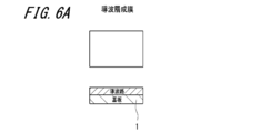
- FIGS. 6A to 6E are diagrams for explaining the procedure for forming the recess 8.
- the upper part of FIGS. 6A to 6E shows a plan view of a portion where one recess 8 is formed. Further, the lower part of FIGS. 6A to 6E shows a cross-sectional view corresponding to the upper part.
- a film was formed on the upper surface 2 of the substrate 1 to form the optical waveguide layer 5, and a resist was applied on the formed film of the optical waveguide layer 5 as shown in FIG. As shown, the applied resist is exposed and developed.
- FIG. 6D the optical waveguide layer 5 is etched to form a space for accommodating the light emitting element 10, and then the resist is removed as shown in FIG. 6E to form the recess 8.
- the recess 8 penetrates from the third surface 3b to the second surface 3a, but the present invention is not necessarily limited to this.
- the recess 8 By forming the recess 8 by etching in this way, even if the pattern of the photomask is a rectangle covered at a right angle, the curved corner support surfaces 9ab and 9bc are affected by the exposure resolution of photolithography and the erosion by etching. , 9cd, 9ad can be formed.
- FIG. 7 is an enlarged plan view of the periphery of the element.
- the radius of curvature r of the corner support surfaces 9ab, 9bc, 9cd, and 9ad can be made smaller than R.
- the light emitting element 10 can be accurately positioned and supported without rotating in the recess 8.
- the lid 11 When the lid 11 is held, the lid 11 covers the recess 8 and may be located on the third surface 3b of the clad 3. At this time, a seal ring 17 (second metal body) is interposed between the lid 11 and the clad 3.
- the seal ring 17 contains a metal material and surrounds the recess 8, and is provided, for example, in an uninterrupted annular shape.
- the lid 11 may be joined to the clad 3 by heating, and the clad 3 and the core 4 are distorted by the stress during the heat joining, so that the optical axis shifts between the light emitting element 10 and the core 4. May occur.
- the mechanical strength around the recess 8 can be improved, and the distortion of the clad 3 and the core 4 can be reduced.
- the optical waveguide package 100 has less optical axis deviation between the light emitting element 10 and the core 4.
- the lid 11 is made of a glass material such as quartz, borosilicate, or sapphire.
- the seal ring 17 is made of, for example, a metal such as Ti, Ni, Au, Pt or Cr, or two or more metals selected from these, and can be deposited, sputtered, ion plated, plated, or the like. It is fixed on the third surface 3b of the clad 3.
- the lid 11 uses a seal ring 17 and a bonding material such as Au-Sn-based or Sn-Ag-Cu-based solder, a metal-based nanoparticle paste such as Ag or Cu, or a glass paste, and is heat-cured or bonded. It may be joined by laser welding or the like.
- the seal ring 17 may be provided not on the clad 3 but on the portion of the lid 11 facing the clad 3.
- the seal ring 17 is composed of, for example, a metal such as Ti, Ni, Au, Pt or Cr, or two or more kinds of metals selected from these, and is composed of vapor deposition, sputtering, ion plating or plating. It may be fixed to the lid 11 by such means.
- the clad 3 uses a seal ring 17 and a bonding material such as Au-Sn-based or Sn-Ag-Cu-based solder, a metal-based nanoparticle paste such as Ag or Cu, or a glass paste, and is thermally cured or laser-coated. It may be joined by welding or the like.
- the seal ring 17 may be provided on both the clad 3 and the lid 11.
- the seal rings 17 provided on the clad 3 and the lid 11 are, for example, Au-Sn-based, Sn-Ag-Cu-based solder, metal-based nanoparticle paste such as Ag or Cu, or glass paste. It may be joined using a joining material such as. The joining may be performed by thermosetting joining, laser welding, or the like.
- FIG. 8 is a plan view showing a light emitting device according to another embodiment of the present disclosure.
- the same reference numerals are given to the parts corresponding to the above-described embodiments, and duplicate description will be omitted.
- each corner support surface 9ab, 9bc, 9cd, 9ad is formed of a flat surface. By making the corner support surfaces 9ab, 9bc, 9cd, and 9ad flat, the light emitting element 10 can be supported by line contact, and the rotation of the light emitting element 10 can be further reduced.
- the portion where the corner support surfaces 9ab, 9bc, 9cd, 9ad and the wall surfaces 7a, 7b, 7c, 7d intersect, and the boundary thereof may be curved. Due to the curved surface shape, it is possible to reduce damage caused by cracks on the wall surfaces 7a, 7b, 7c, 7d and the like due to thermal stress.
- the curved surface shape means that the inner edge near the corner portion is curved in a plan view, and the curved portion is a surface shape extending in the depth direction of the concave portion 8. As the width of each corner support surface 9ab, 9bc, 9cd, 9ad becomes smaller, the distance between the optical waveguide layer 5 and the light emitting element 10 becomes shorter. The bonding efficiency is excellent and each recess 8 becomes small.
- FIG. 9 is a plan view showing a light emitting device according to still another embodiment of the present disclosure.
- the same reference numerals are given to the parts corresponding to the above-described embodiments, and duplicate description will be omitted.
- the wall surfaces 7a to 7d project toward the center of the recess 8, that is, toward the side surface of the light emitting element 10 housed in the recess 8, and the intermediate support surfaces 12a, 12b, 12c, 12d. have.
- Light is emitted by providing protruding intermediate support surfaces 12a, 12b, 12c, 12d so as to come into contact with the light emitting element 10 from sides other than the corner support surfaces 9ab, 9bc, 9cd, and 9ad of the wall surfaces 7a to 7d.
- the portion that makes line contact with the element 10 increases, and the supportability is improved.
- the optical waveguide package 100 has less misalignment of the light emitting element 10 when the light emitting element 10 is mounted.
- the core 4 may be brought closer to the emitting surface of the light emitting element 10 or may be projected to the extent that it touches.
- the optical waveguide package 100 is excellent in the coupling efficiency of optical coupling.
- FIG. 10 is a plan view showing a light emitting device according to still another embodiment of the present disclosure.
- each recess 8 has a first space 13 in which the light emitting element 10 is fitted and a second space 14 connected to the first space 13.
- the second space 14 is an additional space protruding from the first space 13 so as to be connected to the wall surfaces 7a, 7b, 7c, 7d other than the corner support surfaces 9ab, 9bc, 9cd, and 9ad.
- an electrode 15 for supplying power can be provided while maintaining the support function of the light emitting element 10.
- the electrode 15 extends from the element mounting portion 6 between the first surface 2 of the substrate 1 and the second surface 3a of the clad 3.
- One end of the electrode 15 is located in the first space 13 and the second space 14, and the other end is located in the external space, so that the outer space 13 and the second space 14 are kept airtight. It enables electrical connection with power supply circuits and the like.
- Such an electrode 15 may be composed of, for example, two parallel strips of wiring.
- One strip-shaped wiring can be electrically connected from the upper surface electrode of the light emitting element 10 to one end thereof by providing a metal wiring 16 such as wire bonding.
- One end of the other strip-shaped wiring is connected to the element mounting portion 6, and can be electrically connected to the lower surface electrode of the light emitting element 10 via the element mounting portion 6.
- FIG. 11 is a plan view showing a light emitting device according to still another embodiment of the present disclosure.
- the edge of the recess 8 is separated from the seal ring 17 in a plan view.
- the seal ring 17 is a portion to which heat is applied. Since the recess 8 and the seal ring 17 are separated from each other, the space between the portion heated in the clad 3 and the recess 8 is also large, and the distortion of the clad 3 and the core 4 due to thermal stress is reduced. As a result, the optical waveguide package 100 has less optical axis deviation between the light emitting element 10 and the core 4.
- FIG. 12 is a plan view showing a light emitting device according to still another embodiment of the present disclosure.
- the same reference numerals are given to the parts corresponding to the above-described embodiments, and duplicate description will be omitted.
- the recess 8 has a substantially rectangular opening, and has a first side 8a closest to the core 4 and a second side 8b located opposite to the first side 8a in a plan view.
- the distance d1 between the first side 8a of the recess 8 and the seal ring 17 is larger than the distance d2 between the second side 8b and the seal ring 17.
- the optical axis shift between the light emitting element 10 and the core 4 can be further reduced by increasing the distance between the heated seal ring 17 portion and the recess 8 on the side where the core 4 is located.
- the optical waveguide package 100 having such a configuration has a small optical axis deviation between the light emitting element 10 and the core 4.
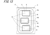
- FIG. 13 is a plan view showing a light emitting device according to still another embodiment of the present disclosure.
- a plurality of element mounting portions 6 are located in a plan view, and a partition 18 for partitioning the plurality of element mounting portions 6 is provided.
- a partition 18 by a clad 3 is provided as in the present embodiment. You just have to do it.
- the element mounting portions 6 are independent of each other by the partition 18, and the influence of stray light in the recess 8 can be reduced, for example. It can be said that each of the plurality of element mounting portions 6 is located in the individual recesses 8 having the corner support surfaces 9ab, 9bc, 9cd, and 9ad by the partition 18. The presence of the partition 18 disperses the thermal stress.
- a plurality of element mounting portions 6 are further arranged side by side in a second direction intersecting the first direction in which the core 4 extends in a plan view, and adjacent element mounting portions 6 are staggered in a plan view. To position.
- the thermal stress is further dispersed and the distortion of the clad 3 and the core 4 can be reduced, so that the optical waveguide package 100 is the light between the light emitting element 10 and the core 4. There is little misalignment.
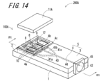
- FIG. 14 is a development view showing a light emitting device 200A according to still another embodiment of the present disclosure.
- FIG. 15 is a perspective view in which the lid of the light emitting device 200A shown in FIG. 14 is omitted.
- FIG. 16 is a cross-sectional view of the light emitting device 200A as seen from the cut plane line XVI-XVI of FIG.
- the same reference numerals are given to the parts corresponding to the above-described embodiments, and duplicate description will be omitted.
- the configuration in which the upper portion of the light emitting element 10 protrudes from each recess 8 and the box-shaped lid 11 is used so as to cover the light emitting element 10 has been described.
- the entire light emitting element 10 is housed in the recess 8, and the recess 8 is a plate-shaped lid. It may be covered with 11A and sealed.
- the configuration of the lid 11A can be simplified.
- a light emitting element 10 connected by a flip chip it is possible to connect to the electrode 15 only on the lower surface and to connect to an external power supply circuit via the electrode 15.
- the light emitting element 10 is not limited to a light emitting diode (Light Emitting Diode; LED), and is, for example, an LD (Laser Diode) or a VCSEL (Vertical Cavity Surface Emitting Laser). You may.
- a light emitting diode Light Emitting Diode; LED
- LD Laser Diode
- VCSEL Vertical Cavity Surface Emitting Laser
- Substrate 2 First surface (upper surface) 3 Clad 3a 2nd surface 3b 3rd surface 4 Core 4a, 4b, 4c Incident end surface 5
- Optical waveguide layer 6 Element mounting part 7 Inner wall surface 7a, 7b, 7c, 7d Wall surface 8 Recession 8a 1st side 8b 2nd side 9ab, 9bc, 9cd, 9ad Square support surface 10
- Light emitting element 11 11A Lid body 15
- Electrode (first metal body) 17 Seal ring (second metal body) 18 Partition 20
- Lens 100 100A
Landscapes
- Physics & Mathematics (AREA)
- General Physics & Mathematics (AREA)
- Optics & Photonics (AREA)
- Condensed Matter Physics & Semiconductors (AREA)
- Electromagnetism (AREA)
- Engineering & Computer Science (AREA)
- Microelectronics & Electronic Packaging (AREA)
- Optical Couplings Of Light Guides (AREA)
- Optical Integrated Circuits (AREA)
- Semiconductor Lasers (AREA)
- Led Device Packages (AREA)
Priority Applications (4)
| Application Number | Priority Date | Filing Date | Title |
|---|---|---|---|
| EP20872053.2A EP4040516A4 (en) | 2019-09-30 | 2020-09-29 | Optical waveguide package and light emitting device |
| US17/761,819 US20220390689A1 (en) | 2019-09-30 | 2020-09-29 | Optical waveguide package and light-emitting device |
| JP2021551336A JP7300794B2 (ja) | 2019-09-30 | 2020-09-29 | 光導波路パッケージおよび発光装置 |
| CN202080065201.3A CN114424099A (zh) | 2019-09-30 | 2020-09-29 | 光波导封装件以及发光装置 |
Applications Claiming Priority (4)
| Application Number | Priority Date | Filing Date | Title |
|---|---|---|---|
| JP2019-180925 | 2019-09-30 | ||
| JP2019180925 | 2019-09-30 | ||
| JP2020110002 | 2020-06-25 | ||
| JP2020-110002 | 2020-06-25 |
Publications (1)
| Publication Number | Publication Date |
|---|---|
| WO2021065948A1 true WO2021065948A1 (ja) | 2021-04-08 |
Family
ID=75336933
Family Applications (1)
| Application Number | Title | Priority Date | Filing Date |
|---|---|---|---|
| PCT/JP2020/037008 Ceased WO2021065948A1 (ja) | 2019-09-30 | 2020-09-29 | 光導波路パッケージおよび発光装置 |
Country Status (5)
| Country | Link |
|---|---|
| US (1) | US20220390689A1 (https=) |
| EP (1) | EP4040516A4 (https=) |
| JP (1) | JP7300794B2 (https=) |
| CN (1) | CN114424099A (https=) |
| WO (1) | WO2021065948A1 (https=) |
Cited By (7)
| Publication number | Priority date | Publication date | Assignee | Title |
|---|---|---|---|---|
| WO2022250118A1 (ja) * | 2021-05-28 | 2022-12-01 | 京セラ株式会社 | 光源モジュール |
| JPWO2022250092A1 (https=) * | 2021-05-28 | 2022-12-01 | ||
| WO2023033107A1 (ja) * | 2021-09-01 | 2023-03-09 | 京セラ株式会社 | 光導波路パッケージおよび発光装置 |
| JPWO2023100927A1 (https=) * | 2021-11-30 | 2023-06-08 | ||
| WO2023179967A1 (de) * | 2022-03-24 | 2023-09-28 | Ams-Osram International Gmbh | Optoelektronisches bauelement |
| WO2024048686A1 (ja) * | 2022-08-31 | 2024-03-07 | 京セラ株式会社 | 光導波路パッケージ |
| WO2025070158A1 (ja) * | 2023-09-28 | 2025-04-03 | 京セラ株式会社 | 光導波路基板、電子素子収納用パッケージ、電子モジュール及び電子デバイス |
Families Citing this family (1)
| Publication number | Priority date | Publication date | Assignee | Title |
|---|---|---|---|---|
| CN111323878B (zh) * | 2020-04-01 | 2021-10-15 | 联合微电子中心有限责任公司 | 一种激光器芯片与硅基光电子芯片的耦合对准装置及方法 |
Citations (10)
| Publication number | Priority date | Publication date | Assignee | Title |
|---|---|---|---|---|
| JPS6146911A (ja) | 1984-08-10 | 1986-03-07 | Nippon Telegr & Teleph Corp <Ntt> | 導波形光モジユ−ル |
| JPH05167060A (ja) * | 1991-12-12 | 1993-07-02 | Nec Corp | 光結合回路 |
| US5454055A (en) * | 1992-09-29 | 1995-09-26 | Robert Bosch Gmbh | Method of making a cover for an integrated optical circuit, cover for an integrated optical circuit, and integrated optical circuit made with this cover |
| JPH08110446A (ja) * | 1994-10-12 | 1996-04-30 | Hitachi Ltd | 光伝送モジュール |
| JPH0961651A (ja) * | 1995-06-14 | 1997-03-07 | Nippon Telegr & Teleph Corp <Ntt> | ハイブリッド光集積回路 |
| JPH09512353A (ja) * | 1995-02-07 | 1997-12-09 | エルディティ ゲーエムベーハー ウント シーオー.レーザー−ディスプレー−テクノロギー カーゲー | カラー画像形成システム及びその使用方法 |
| JP2001174655A (ja) * | 1999-12-15 | 2001-06-29 | Opnext Japan Inc | 双方向通信光モジュール用素子及びその検査方法 |
| JP2004258268A (ja) * | 2003-02-25 | 2004-09-16 | Tdk Corp | 埋込型光部品及びその製造方法並びに埋込型光部品を用いた光回路 |
| JP2007328201A (ja) * | 2006-06-08 | 2007-12-20 | Nippon Telegr & Teleph Corp <Ntt> | 光集積回路 |
| JP2008516525A (ja) * | 2004-10-05 | 2008-05-15 | トラツキング・テクノロジーズ・インコーポレーテツド | 無線周波識別タグ及びその製造方法 |
Family Cites Families (7)
| Publication number | Priority date | Publication date | Assignee | Title |
|---|---|---|---|---|
| DE19917325C2 (de) * | 1999-04-16 | 2001-06-21 | Siemens Ag | Fassung für opto-elektronische Bauelemente |
| EP1378777A3 (en) * | 2002-07-02 | 2005-02-16 | Omron Corporation | Optical waveguide device, manufacturing method thereof, and optical communication apparatus |
| JP2004117706A (ja) * | 2002-09-25 | 2004-04-15 | Sumitomo Electric Ind Ltd | 光集積素子、光集積素子の製造方法、及び光源モジュール |
| JP2005266179A (ja) * | 2004-03-17 | 2005-09-29 | Omron Corp | 光導波路装置及び光導波路装置の製造方法並びに光導波路装置の中間体 |
| JP5267426B2 (ja) * | 2009-11-04 | 2013-08-21 | 住友ベークライト株式会社 | 光素子搭載基板、光電気混載基板および電子機器 |
| JP2016004224A (ja) * | 2014-06-19 | 2016-01-12 | 富士通株式会社 | 光学モジュール、光学モジュールの製造方法及び光学装置 |
| JP6940749B2 (ja) * | 2016-04-28 | 2021-09-29 | 日亜化学工業株式会社 | 発光装置 |
-
2020
- 2020-09-29 EP EP20872053.2A patent/EP4040516A4/en not_active Withdrawn
- 2020-09-29 JP JP2021551336A patent/JP7300794B2/ja active Active
- 2020-09-29 WO PCT/JP2020/037008 patent/WO2021065948A1/ja not_active Ceased
- 2020-09-29 CN CN202080065201.3A patent/CN114424099A/zh active Pending
- 2020-09-29 US US17/761,819 patent/US20220390689A1/en not_active Abandoned
Patent Citations (10)
| Publication number | Priority date | Publication date | Assignee | Title |
|---|---|---|---|---|
| JPS6146911A (ja) | 1984-08-10 | 1986-03-07 | Nippon Telegr & Teleph Corp <Ntt> | 導波形光モジユ−ル |
| JPH05167060A (ja) * | 1991-12-12 | 1993-07-02 | Nec Corp | 光結合回路 |
| US5454055A (en) * | 1992-09-29 | 1995-09-26 | Robert Bosch Gmbh | Method of making a cover for an integrated optical circuit, cover for an integrated optical circuit, and integrated optical circuit made with this cover |
| JPH08110446A (ja) * | 1994-10-12 | 1996-04-30 | Hitachi Ltd | 光伝送モジュール |
| JPH09512353A (ja) * | 1995-02-07 | 1997-12-09 | エルディティ ゲーエムベーハー ウント シーオー.レーザー−ディスプレー−テクノロギー カーゲー | カラー画像形成システム及びその使用方法 |
| JPH0961651A (ja) * | 1995-06-14 | 1997-03-07 | Nippon Telegr & Teleph Corp <Ntt> | ハイブリッド光集積回路 |
| JP2001174655A (ja) * | 1999-12-15 | 2001-06-29 | Opnext Japan Inc | 双方向通信光モジュール用素子及びその検査方法 |
| JP2004258268A (ja) * | 2003-02-25 | 2004-09-16 | Tdk Corp | 埋込型光部品及びその製造方法並びに埋込型光部品を用いた光回路 |
| JP2008516525A (ja) * | 2004-10-05 | 2008-05-15 | トラツキング・テクノロジーズ・インコーポレーテツド | 無線周波識別タグ及びその製造方法 |
| JP2007328201A (ja) * | 2006-06-08 | 2007-12-20 | Nippon Telegr & Teleph Corp <Ntt> | 光集積回路 |
Non-Patent Citations (1)
| Title |
|---|
| See also references of EP4040516A4 |
Cited By (20)
| Publication number | Priority date | Publication date | Assignee | Title |
|---|---|---|---|---|
| TWI873424B (zh) * | 2021-05-28 | 2025-02-21 | 日商京瓷股份有限公司 | 光源模組 |
| JPWO2022250092A1 (https=) * | 2021-05-28 | 2022-12-01 | ||
| WO2022250092A1 (ja) * | 2021-05-28 | 2022-12-01 | 京セラ株式会社 | 光源モジュール |
| JPWO2022250118A1 (https=) * | 2021-05-28 | 2022-12-01 | ||
| US12292590B2 (en) | 2021-05-28 | 2025-05-06 | Kyocera Corporation | Light source module |
| WO2022250118A1 (ja) * | 2021-05-28 | 2022-12-01 | 京セラ株式会社 | 光源モジュール |
| EP4350401A4 (en) * | 2021-05-28 | 2025-04-30 | Kyocera Corporation | Light source module |
| US12276823B2 (en) | 2021-05-28 | 2025-04-15 | Kyocera Corporation | Light source module |
| JPWO2023033107A1 (https=) * | 2021-09-01 | 2023-03-09 | ||
| TWI865917B (zh) * | 2021-09-01 | 2024-12-11 | 日商京瓷股份有限公司 | 光波導封裝及發光裝置 |
| WO2023033107A1 (ja) * | 2021-09-01 | 2023-03-09 | 京セラ株式会社 | 光導波路パッケージおよび発光装置 |
| WO2023100927A1 (ja) * | 2021-11-30 | 2023-06-08 | 京セラ株式会社 | 光導波路パッケージおよび光源モジュール |
| JPWO2023100927A1 (https=) * | 2021-11-30 | 2023-06-08 | ||
| US12345913B2 (en) | 2021-11-30 | 2025-07-01 | Kyocera Corporation | Optical waveguide package and light source module |
| JP7711212B2 (ja) | 2021-11-30 | 2025-07-22 | 京セラ株式会社 | 光導波路パッケージおよび光源モジュール |
| EP4443207A4 (en) * | 2021-11-30 | 2025-11-19 | Kyocera Corp | OPTICAL WAVEGUIDE BOX AND LIGHT SOURCE MODULE |
| WO2023179967A1 (de) * | 2022-03-24 | 2023-09-28 | Ams-Osram International Gmbh | Optoelektronisches bauelement |
| WO2024048686A1 (ja) * | 2022-08-31 | 2024-03-07 | 京セラ株式会社 | 光導波路パッケージ |
| JPWO2024048686A1 (https=) * | 2022-08-31 | 2024-03-07 | ||
| WO2025070158A1 (ja) * | 2023-09-28 | 2025-04-03 | 京セラ株式会社 | 光導波路基板、電子素子収納用パッケージ、電子モジュール及び電子デバイス |
Also Published As
| Publication number | Publication date |
|---|---|
| JPWO2021065948A1 (https=) | 2021-04-08 |
| US20220390689A1 (en) | 2022-12-08 |
| EP4040516A4 (en) | 2023-11-15 |
| JP7300794B2 (ja) | 2023-06-30 |
| EP4040516A1 (en) | 2022-08-10 |
| CN114424099A (zh) | 2022-04-29 |
Similar Documents
| Publication | Publication Date | Title |
|---|---|---|
| WO2021065948A1 (ja) | 光導波路パッケージおよび発光装置 | |
| JP6944085B2 (ja) | 光導波路パッケージおよび発光装置 | |
| JP7534687B2 (ja) | 発光モジュールの製造方法、発光モジュール及びプロジェクタ | |
| JP2023127591A (ja) | 光導波路パッケージおよび発光装置 | |
| WO2021261232A1 (ja) | 光導波路パッケージ、発光装置および投影システム | |
| WO2021241332A1 (ja) | 光導波路パッケージおよび発光装置 | |
| CN115380232A (zh) | 光波导模块以及光源模块 | |
| EP4400879A1 (en) | Light-emitting device | |
| WO2023153419A1 (ja) | 光導波路基板、光導波路パッケージおよび光源モジュール | |
| US12276823B2 (en) | Light source module | |
| US20250306319A1 (en) | Optical waveguide package and light-emitting device | |
| CN117396785A (zh) | 光源模块 | |
| TW202346930A (zh) | 光波導基板、光波導封裝及光源模組 | |
| TW202443215A (zh) | 光波導封裝及光源模組 | |
| WO2023033107A1 (ja) | 光導波路パッケージおよび発光装置 | |
| JP2021071647A (ja) | 光導波路パッケージおよび発光装置 | |
| JP2021086050A (ja) | 光導波路モジュール |
Legal Events
| Date | Code | Title | Description |
|---|---|---|---|
| 121 | Ep: the epo has been informed by wipo that ep was designated in this application |
Ref document number: 20872053 Country of ref document: EP Kind code of ref document: A1 |
|
| ENP | Entry into the national phase |
Ref document number: 2021551336 Country of ref document: JP Kind code of ref document: A |
|
| NENP | Non-entry into the national phase |
Ref country code: DE |
|
| ENP | Entry into the national phase |
Ref document number: 2020872053 Country of ref document: EP Effective date: 20220502 |