WO2021053952A1 - 撮像素子および撮像装置 - Google Patents
撮像素子および撮像装置 Download PDFInfo
- Publication number
- WO2021053952A1 WO2021053952A1 PCT/JP2020/027703 JP2020027703W WO2021053952A1 WO 2021053952 A1 WO2021053952 A1 WO 2021053952A1 JP 2020027703 W JP2020027703 W JP 2020027703W WO 2021053952 A1 WO2021053952 A1 WO 2021053952A1
- Authority
- WO
- WIPO (PCT)
- Prior art keywords
- pixel
- semiconductor substrate
- region
- image pickup
- pixels
- Prior art date
- Legal status (The legal status is an assumption and is not a legal conclusion. Google has not performed a legal analysis and makes no representation as to the accuracy of the status listed.)
- Ceased
Links
Images





Classifications
-
- G—PHYSICS
- G02—OPTICS
- G02B—OPTICAL ELEMENTS, SYSTEMS OR APPARATUS
- G02B5/00—Optical elements other than lenses
- G02B5/30—Polarising elements
-
- H—ELECTRICITY
- H04—ELECTRIC COMMUNICATION TECHNIQUE
- H04N—PICTORIAL COMMUNICATION, e.g. TELEVISION
- H04N25/00—Circuitry of solid-state image sensors [SSIS]; Control thereof
- H04N25/60—Noise processing, e.g. detecting, correcting, reducing or removing noise
- H04N25/62—Detection or reduction of noise due to excess charges produced by the exposure, e.g. smear, blooming, ghost image, crosstalk or leakage between pixels
-
- H—ELECTRICITY
- H04—ELECTRIC COMMUNICATION TECHNIQUE
- H04N—PICTORIAL COMMUNICATION, e.g. TELEVISION
- H04N25/00—Circuitry of solid-state image sensors [SSIS]; Control thereof
- H04N25/70—SSIS architectures; Circuits associated therewith
-
- H—ELECTRICITY
- H04—ELECTRIC COMMUNICATION TECHNIQUE
- H04N—PICTORIAL COMMUNICATION, e.g. TELEVISION
- H04N25/00—Circuitry of solid-state image sensors [SSIS]; Control thereof
- H04N25/70—SSIS architectures; Circuits associated therewith
- H04N25/76—Addressed sensors, e.g. MOS or CMOS sensors
-
- H—ELECTRICITY
- H10—SEMICONDUCTOR DEVICES; ELECTRIC SOLID-STATE DEVICES NOT OTHERWISE PROVIDED FOR
- H10F—INORGANIC SEMICONDUCTOR DEVICES SENSITIVE TO INFRARED RADIATION, LIGHT, ELECTROMAGNETIC RADIATION OF SHORTER WAVELENGTH OR CORPUSCULAR RADIATION
- H10F39/00—Integrated devices, or assemblies of multiple devices, comprising at least one element covered by group H10F30/00, e.g. radiation detectors comprising photodiode arrays
- H10F39/10—Integrated devices
- H10F39/12—Image sensors
-
- H—ELECTRICITY
- H10—SEMICONDUCTOR DEVICES; ELECTRIC SOLID-STATE DEVICES NOT OTHERWISE PROVIDED FOR
- H10F—INORGANIC SEMICONDUCTOR DEVICES SENSITIVE TO INFRARED RADIATION, LIGHT, ELECTROMAGNETIC RADIATION OF SHORTER WAVELENGTH OR CORPUSCULAR RADIATION
- H10F39/00—Integrated devices, or assemblies of multiple devices, comprising at least one element covered by group H10F30/00, e.g. radiation detectors comprising photodiode arrays
- H10F39/80—Constructional details of image sensors
- H10F39/803—Pixels having integrated switching, control, storage or amplification elements
- H10F39/8033—Photosensitive area
-
- H—ELECTRICITY
- H10—SEMICONDUCTOR DEVICES; ELECTRIC SOLID-STATE DEVICES NOT OTHERWISE PROVIDED FOR
- H10F—INORGANIC SEMICONDUCTOR DEVICES SENSITIVE TO INFRARED RADIATION, LIGHT, ELECTROMAGNETIC RADIATION OF SHORTER WAVELENGTH OR CORPUSCULAR RADIATION
- H10F39/00—Integrated devices, or assemblies of multiple devices, comprising at least one element covered by group H10F30/00, e.g. radiation detectors comprising photodiode arrays
- H10F39/80—Constructional details of image sensors
- H10F39/805—Coatings
- H10F39/8053—Colour filters
-
- H—ELECTRICITY
- H10—SEMICONDUCTOR DEVICES; ELECTRIC SOLID-STATE DEVICES NOT OTHERWISE PROVIDED FOR
- H10F—INORGANIC SEMICONDUCTOR DEVICES SENSITIVE TO INFRARED RADIATION, LIGHT, ELECTROMAGNETIC RADIATION OF SHORTER WAVELENGTH OR CORPUSCULAR RADIATION
- H10F39/00—Integrated devices, or assemblies of multiple devices, comprising at least one element covered by group H10F30/00, e.g. radiation detectors comprising photodiode arrays
- H10F39/80—Constructional details of image sensors
- H10F39/805—Coatings
- H10F39/8057—Optical shielding
-
- H—ELECTRICITY
- H10—SEMICONDUCTOR DEVICES; ELECTRIC SOLID-STATE DEVICES NOT OTHERWISE PROVIDED FOR
- H10F—INORGANIC SEMICONDUCTOR DEVICES SENSITIVE TO INFRARED RADIATION, LIGHT, ELECTROMAGNETIC RADIATION OF SHORTER WAVELENGTH OR CORPUSCULAR RADIATION
- H10F39/00—Integrated devices, or assemblies of multiple devices, comprising at least one element covered by group H10F30/00, e.g. radiation detectors comprising photodiode arrays
- H10F39/80—Constructional details of image sensors
- H10F39/806—Optical elements or arrangements associated with the image sensors
Definitions
- the present disclosure relates to an image pickup device and an image pickup device. More specifically, the present invention relates to an image pickup device that acquires polarization information of a subject and an image pickup device that uses the image pickup device.
- an image sensor that acquires polarization information of a subject has been used.
- polarization information By acquiring the polarization information, it is possible to detect incident light in a specific polarization direction, for example, reflected light from a water pool or a glass surface, and remove the incident light in the specific polarization direction. It is possible to improve the image quality of the image captured by the image sensor. It is also possible to acquire the three-dimensional shape of the surface of the subject by using the polarization information.
- Polarization information can be acquired by arranging a polarizing portion that transmits incident light in a specific polarization direction on the pixels of the image sensor. As this polarizing portion, a polarizing portion configured by a wire grid can be used.
- This wire grid is formed by arranging a plurality of strip-shaped conductors based on a predetermined pitch.
- the incident light in the polarization direction parallel to the arrangement direction of the plurality of band-shaped conductors is transmitted through the polarizing part by the wire grid, and the incident light in the polarization direction perpendicular to the arrangement direction of the plurality of band-shaped conductors is reflected and attenuated by the polarization part. Will be done.
- an image pickup device for example, an image pickup device having a light-shielding film surrounding the photoelectric conversion element in a semiconductor substrate on which a photoelectric conversion element for each pixel is arranged and having a polarizing portion arranged on the back surface of the semiconductor substrate is used.
- the light-shielding films are arranged in a grid pattern so as to fill the space between adjacent pixels.
- the light-shielding film is made of a conductive light-shielding material and is connected to a band-shaped conductor constituting the polarizing portion, and a negative bias voltage is applied to the polarizing portion via the light-shielding film. This bias voltage gives a negative potential to the back surface of the semiconductor substrate, and the pinning on the back surface side of the semiconductor substrate is strengthened.
- the above-mentioned conventional technique has a problem that crosstalk between pixels increases.
- the above-mentioned light-shielding film is formed by forming grid-like grooves in a semiconductor substrate by etching and embedding a conductive light-shielding material such as metal in the grooves.
- a microloading phenomenon occurs at the intersection of the vertical and horizontal grooves forming the lattice, and the groove becomes deep. Therefore, the grooves other than the intersections become relatively shallow, and the depth of the light-shielding film after formation becomes insufficient.
- crosstalk increases due to leakage of incident light to adjacent pixels. Due to this crosstalk, the error of the polarization information increases, and the image quality of the image captured by the image sensor deteriorates.
- the present disclosure has been made in view of the above-mentioned problems, and an object of the present disclosure is to reduce crosstalk between adjacent pixels in an image pickup device that acquires polarization information of a subject.
- the present disclosure has been made to solve the above-mentioned problems, and the first aspect thereof is the polarized light incident formed on a polarizing portion and a semiconductor substrate that polarize the incident light in a specific polarization direction. It is formed in a plurality of pixels including a photoelectric conversion unit that performs photoelectric conversion of light, a separation region arranged on the semiconductor substrate to separate the plurality of pixels, and the separation region near the corners of the pixels. It is an image pickup device including a non-separable region formed of the semiconductor substrate in the gap portion.
- the polarizing portion may polarize the incident light by transmitting the incident light in a specific polarization direction among the incident lights.
- the polarizing portion may be composed of a wire grid composed of a plurality of strip-shaped conductors arranged at a predetermined pitch.
- the non-separable region may be arranged between the plurality of pixels having polarization portions in the specific polarization directions that are not orthogonal to each other.
- the separation region may be formed in a recess formed in the semiconductor substrate.
- the separation region may have a member that blocks the incident light.
- the separation region may have a member made of metal.
- the separation region may have an insulating member.
- the non-separable region may be composed of the semiconductor substrate in the gap portion of the gap of approximately 10% of the width of the surface of the pixel irradiated with the incident light.
- the non-separable region may be composed of the semiconductor substrate in the gap portion having a gap substantially equal to the width of the surface of the separated region to which the incident light is irradiated.
- a second pixel which is the pixel not provided with the polarizing portion, may be further provided.
- the non-separable region may be arranged between the pixel and the second pixel.
- a second aspect of the present disclosure includes a plurality of pixels including a polarizing unit that polarizes incident light in a specific polarization direction and a photoelectric conversion unit formed on a semiconductor substrate that performs photoelectric conversion of the polarized incident light.
- a separation region arranged on the semiconductor substrate to separate the plurality of pixels from each other, and a non-separation region formed by the semiconductor substrate in a gap portion formed in the separation region near the corner of the pixel.
- It is an image pickup apparatus including a processing circuit for processing an image signal generated based on the above-mentioned photoelectric conversion.
- the non-separable region is arranged adjacent to the separated region of the region where the pixel boundaries intersect.
- FIG. 1 is a diagram showing a configuration example of an image sensor according to an embodiment of the present disclosure.
- the image sensor 1 in the figure includes a pixel array unit 10, a vertical drive unit 20, a column signal processing unit 30, and a control unit 40.
- the pixel array unit 10 is configured by arranging the pixels 100 in a two-dimensional grid pattern.
- the pixel 100 generates an image signal according to the irradiated light.
- the pixel 100 has a photoelectric conversion unit that generates an electric charge according to the irradiated light.
- the pixel 100 further has a pixel circuit. This pixel circuit generates an image signal based on the electric charge generated by the photoelectric conversion unit. The generation of the image signal is controlled by the control signal generated by the vertical drive unit 20 described later.
- the signal lines 11 and 12 are arranged in the pixel array unit 10 in an XY matrix.
- the signal line 11 is a signal line that transmits a control signal of the pixel circuit in the pixel 100, is arranged for each line of the pixel array unit 10, and is commonly wired to the pixel 100 arranged in each line.
- the signal line 12 is a signal line for transmitting an image signal generated by the pixel circuit of the pixel 100, is arranged in each row of the pixel array unit 10, and is commonly wired to the pixel 100 arranged in each row. To. These photoelectric conversion units and pixel circuits are formed on a semiconductor substrate.
- the vertical drive unit 20 generates a control signal for the pixel circuit of the pixel 100.
- the vertical drive unit 20 transmits the generated control signal to the pixel 100 via the signal line 11 in the figure.
- the column signal processing unit 30 processes the image signal generated by the pixel 100.
- the column signal processing unit 30 processes the image signal transmitted from the pixel 100 via the signal line 12 in the figure.
- the processing in the column signal processing unit 30 corresponds to, for example, analog-to-digital conversion that converts an analog image signal generated in the pixel 100 into a digital image signal.
- the image signal processed by the column signal processing unit 30 is output as an image signal of the image sensor 1.
- the control unit 40 controls the entire image sensor 1.
- the control unit 40 controls the image sensor 1 by generating and outputting a control signal for controlling the vertical drive unit 20 and the column signal processing unit 30.
- the control signal generated by the control unit 40 is transmitted to the vertical drive unit 20 and the column signal processing unit 30 by the signal lines 41 and 42, respectively.
- the column signal processing unit 30 is an example of the processing circuit described in the claims.
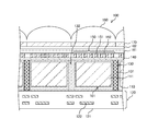
- FIG. 2 is a diagram showing a configuration example of pixels according to the first embodiment of the present disclosure.
- FIG. 6 is a schematic cross-sectional view showing a configuration example of the pixel 100.
- Pixels 100 in the figure include a semiconductor substrate 110, a wiring region 120, a separation region 131, a non-separation region 132, insulating films 140 and 161, a polarizing portion 150, a protective film 162, and a color filter 170. It includes an on-chip lens 180.
- the semiconductor substrate 110 is a semiconductor substrate on which a diffusion region of elements such as a photoelectric conversion unit and a pixel circuit is formed.
- a semiconductor substrate made of silicon (Si) can be used for the semiconductor substrate 110.
- the diffusion region of the elements of the photoelectric conversion unit and the pixel circuit is formed in the well region formed on the semiconductor substrate 110.
- the semiconductor substrate 110 in the figure is assumed to be configured in a p-type well region. By arranging the n-type semiconductor region in the p-type well region, it is possible to form a diffusion region of the elements of the photoelectric conversion unit and the pixel circuit.
- the photoelectric conversion unit 101 is shown as an example of these.
- the photoelectric conversion unit 101 is composed of an n-type semiconductor region 111 arranged on the semiconductor substrate 110 in the figure. Specifically, a photodiode formed by a pn junction at the interface between the n-type semiconductor region 111 and the surrounding p-type well region corresponds to the photoelectric conversion unit 101.
- a photodiode formed by a pn junction at the interface between the n-type semiconductor region 111 and the surrounding p-type well region corresponds to the photoelectric conversion unit 101.
- an electric charge is generated by photoelectric conversion.
- the electrons of this charge are accumulated in the n-type semiconductor region 111. Based on the accumulated charges (electrons), an image signal is generated by a pixel circuit (not shown).
- the wiring area 120 is an area arranged adjacent to the surface of the semiconductor substrate 110 and forming a wiring for transmitting a signal to an element or the like of a pixel circuit of the pixel 100.
- the wiring area 120 in the figure is composed of a wiring layer 122 and an insulating layer 121.
- the wiring layer 122 is a wiring for transmitting a signal.
- the wiring layer 122 can be made of, for example, a metal such as copper (Cu).
- the insulating layer 121 insulates the wiring layer 122.
- the insulating layer 121 can be made of, for example, silicon oxide (SiO 2 ) or silicon nitride (SiN).
- the insulating film 140 is a film that is arranged adjacent to the back surface of the semiconductor substrate 110 and protects the back surface of the semiconductor substrate 110.
- the insulating film 140 can be made of, for example, SiO 2 or SiN.
- a fixed charge film that pins the interface state of the semiconductor substrate 110 can also be arranged between the semiconductor substrate 110 and the insulating film 140.
- As the fixed charge film for example, a film of hafnium oxide (HfO 2 ) can be used.
- the polarizing unit 150 is arranged on the surface of the insulating film 140 to polarize the incident light from the subject in a specific polarization direction.
- a polarizing unit that polarizes the incident light by transmitting the incident light in a specific polarization direction can be used.
- the polarizing unit 150 in the figure represents an example of a polarizing unit composed of a wire grid. This wire grid is a polarizing portion formed by arranging a plurality of strip-shaped conductors at a predetermined pitch.
- the polarizing portion 150 in the figure is configured by arranging strip-shaped conductors 151.
- a dielectric material such as air can be arranged in the region 152 between the plurality of strip conductors 151.
- the incident light in the polarization direction perpendicular to the arrangement direction of the band-shaped conductors 151 is attenuated by the polarizing unit 150. This is because the electric charge inside the band-shaped conductor 151 vibrates due to the incident light to generate reflected light.
- the incident light in the polarization direction parallel to the arrangement direction of the band-shaped conductors 151 that is, the polarization direction perpendicular to the band-shaped conductors 151, passes through the polarizing portion 150. This is because the vibration of the electric charge inside the strip conductor 151 is limited.
- the polarization direction transmitted through the polarizing unit 150 is referred to as a transmission axis.
- the ratio of the maximum transmitted light to the minimum transmitted light among the transmitted light of the polarizing unit 150 is called an extinction ratio.
- the polarizing unit 150 transmits light in a specific polarization direction (transmission axis).
- the polarizing unit 150 attenuates light in a polarization direction different from the transmission axis.
- the maximum amount of attenuation is the transmitted light in the polarization direction that differs by 90 degrees from the transmission axis.
- the ratio of the maximum value and the minimum value of such transmitted light is the extinction ratio. The higher the extinction ratio, the less noise the polarization information can be acquired.
- Crosstalk can be reduced by arranging the polarizing portion 150 adjacent to the back surface of the semiconductor substrate 110 on which the separation region 131 described later is arranged.
- the polarizing portion 150 in the figure is arranged adjacent to the back surface of the semiconductor substrate 110 via the insulating film 140.
- the insulating film 161 is a film that insulates the polarizing portion 150. Further, the insulating film 161 further protects the strip-shaped conductor 151 of the polarizing portion 150.
- the insulating film 161 can be made of, for example, SiO 2 .
- the protective film 162 is a film that protects and flattens the back surface of the semiconductor substrate 110. By arranging the protective film 162, the surface on which the color filter 170, which will be described later, is arranged is flattened, and the occurrence of color unevenness can be prevented.
- the color filter 170 is an optical filter that transmits light of a predetermined wavelength among the incident light. By arranging the color filter 170, a color image signal can be generated.
- a color filter that transmits red light, green light, and blue light can be used.
- the on-chip lens 180 is a lens that is arranged for each pixel 100 and collects incident light.
- the on-chip lens 180 is configured in a hemispherical shape and collects incident light on a photoelectric conversion unit 101 (n-type semiconductor region 111).
- the on-chip lens 180 can be made of, for example, an organic material such as acrylic resin or an inorganic material such as SiN.
- the pixel 100 in the figure is focused by the on-chip lens 180, and the incident light transmitted through the color filter 170 and the polarizing unit 150 is irradiated to the photoelectric conversion unit 101 from the back surface of the semiconductor substrate 110.
- the image pickup device 1 in which the back surface of the semiconductor substrate 110 is irradiated with incident light is referred to as a backside irradiation type image pickup device.
- the surface irradiated with the incident light of the image sensor 1 is referred to as an incident surface.
- a separation region 131 is arranged at the boundary of the pixels 100 on the semiconductor substrate 110.
- the separation region 131 is configured to surround the semiconductor substrate 110 of the pixel 100 and separates the pixel 100.
- crosstalk means that the image signal changes under the influence of adjacent pixels 100, which causes noise in the image signal.
- the separation region 131 in the figure can be configured, for example, by embedding a separation member in a groove-shaped recess 130 formed in the semiconductor substrate 110.
- the separation region 131 in the figure shows an example in which the pixels 100 on the back surface, which is the incident surface of the semiconductor substrate 110, are separated and formed at a depth that does not reach the front surface from the back surface of the semiconductor substrate 110.
- a member that blocks incident light as a member for separation. This is because it is possible to prevent leakage of incident light from adjacent pixels 100 and further reduce crosstalk. Specifically, it is possible to prevent the occurrence of color mixing by preventing the incident of light transmitted through the color filters 170 corresponding to different wavelengths in the adjacent pixels 100.
- color mixing is a phenomenon in which image signals of different colors are mixed, and is an example of crosstalk.
- by arranging the separation region 131 formed by the member that blocks the incident light it is possible to prevent the incident light polarized in different directions by the polarizing portion 150 in the adjacent pixel 100 from being incident. It is possible to prevent the above-mentioned decrease in the extinction ratio.
- a metal material such as tungsten (W), aluminum (Al), and copper (Cu) can be used.
- the separation region 131 in the figure is formed by arranging an insulating film on the inner wall of the recess 130 formed at the boundary portion of the pixel 100 in the semiconductor substrate 110 and embedding the above-mentioned metal material W.
- a non-separable region 132 is further arranged on the semiconductor substrate 110 at the boundary of the pixel 100.
- the non-separable region 132 is composed of the semiconductor substrate 110 in the gap portion of the above-mentioned separated region 131.
- the broken line rectangle of the semiconductor substrate 110 in the figure represents the non-separable region 132.
- the gap portion of the separation region 131 is arranged in the vicinity of the corner portion of the pixel 100. Details of the configuration of the separated region 131 and the non-separated region 132 will be described later.
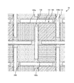
- FIG. 3 is a diagram showing a configuration example of a separation region according to the first embodiment of the present disclosure.
- the figure is a plan view seen from an incident surface of a plurality of pixels 100 arranged in the pixel array unit 10, and is a plan view showing a configuration example of a separated region 131 and a non-separated region 132.
- the hatched region in the figure represents the back surface of the semiconductor substrate 110.
- the square wave of the alternate long and short dash line represents pixel 100.
- the white square represents the separation region 131.
- the broken line rectangle represents the strip-shaped conductor 151 of the polarizing portion 150. Note that FIG. 2 shows the configuration of the cross section along the line aa'in the figure.
- the figure shows an example of pixels 100 having a rectangular shape in a plan view. Further, in the pixels 100a, 100b, 100c and 100d arranged in 2 rows and 2 columns of the figure, a polarizing unit 150 that polarizes the incident light in different polarization directions is arranged. That is, in the pixels 100a, 100b, 100c and 100d, the polarizing portions 150 having different transmission axes by 45 degrees are arranged.
- the two-row, two-column pixel 100 can detect incident light in four polarization directions and generate an image signal including polarization information in the four directions.
- the separation region 131 is arranged at the boundary between the pixels 100 and is arranged in a shape surrounding the periphery of the pixels 100.
- the non-separable region 132 is arranged in the gap portion of the separated region 131 formed near the corner of the rectangular pixel 100. This gap is formed in the separation region 131 adjacent to the intersection of the vertical and horizontal separation regions 131 arranged in a grid shape in a plan view. As shown in the figure, the separation region 131 is divided by the gap portion of the non-separation region 132 while one of the vertical or horizontal directions penetrates at the intersection where the boundaries of the grid-shaped pixels 100 in the plan view intersect. It is composed of shapes. Further, the non-separable region 132 is arranged adjacent to the intersection of the boundaries of all the pixels 100.
- the separation region 131 is arranged in the recess 130 formed in the semiconductor substrate 110.
- the recess 130 can be formed by etching the back surface of the semiconductor substrate 110.
- the depth variation of the recess 130 can be reduced by arranging the non-separable region 132. This makes it possible to reduce the occurrence of crosstalk due to depth variation. Details of the depth variation of the recess 130 will be described later.
- the non-separable region 132 can be arranged between the pixels 100 in which the polarization directions of the polarizing portions 150 arranged in the pixel 100 are not orthogonal to each other. Specifically, it is arranged between the pixels 100a and 100b in the figure, between the pixels 100b and 100c, between the pixels 100c and 100d, and between the pixels 100d and 100a.
- the non-separable region 132 By arranging the non-separable region 132, incident light leaks between adjacent pixels 100. The incident light transmitted through the polarizing portions 150 in different polarization directions leaks, and the extinction ratio decreases.
- the separation region 131 is arranged between the pixels 100 in which the polarizing portions 150 whose polarization directions are not orthogonal to each other are arranged. Therefore, it is possible to reduce the decrease in the extinction ratio. This will be described by taking the pixel 100a and the pixel 100b as examples.
- a non-separable region 132 is arranged between the pixels 100a and 100b.
- the polarizing portion 150 of the pixel 100b is configured in the polarization direction deviated by 45 degrees with respect to the transmission axis of the polarizing portion 150 of the pixel 100a.
- the incident light in the polarization direction deviated by 45 degrees with respect to the transmission axis of the polarizing unit 150 is attenuated to a light amount of about 50% and transmitted. That is, the incident light transmitted through the polarizing portion 150 of the pixel 100b mixed in the pixel 100a through the non-separable region 132 is the incident light in the polarization direction attenuated to approximately 50% in the polarizing portion 150 of the pixel 100a. Therefore, even when the non-separation region 132 is arranged, the extinction ratio can be only slightly increased.
- the non-separable region 132 is not arranged between the pixels 100 having the polarizing portions 150 whose polarization directions are substantially orthogonal to each other.
- the non-separable region 132 is not arranged between the pixels 100 whose polarization directions differ by 80 to 100 degrees.
- the non-separable region 132 is not arranged between the pixels 100a and 100c and between the pixels 100b and 100d.
- the polarizing unit 150 blocks substantially 100% of incident light in the polarization direction orthogonal to its own transmission axis.
- the extinction ratio is significantly lowered.
- the non-separable region 132 between the pixels 100 in which the polarizing portions 150 in the orthogonal polarization directions are arranged, it is possible to prevent the incident light from being mixed in through the non-separable region 132. It is possible to prevent a decrease in the extinction ratio based on the pixel 100 in which the polarizing portions 150 in the orthogonal polarization directions are arranged.
- FIG. 4 is a diagram showing an example of a recess in the separation region according to the first embodiment of the present disclosure.
- FIG. 6 is a diagram showing an example of the shape of the recess 130, and is a diagram for explaining the effect of the non-separable region 132.
- a and C in the figure are simplified plan views of the semiconductor substrate 110 and the separation region 131 of the pixel 100.
- B and D in the figure are cross-sectional views taken along the aa'line of A and C in the figure, respectively. Note that A and B in the figure are diagrams showing an example in the case where the non-separable region 132 is not arranged for comparison.
- the recess 130 of the separated region 131 has a shape in which the recesses 130 intersect vertically and horizontally in a plan view.
- the recess 130 can be formed by, for example, etching the back surface of the semiconductor substrate 110. Anisotropic dry etching can be applied to this etching. By this anisotropic dry etching, a groove-shaped recess 130 having a high aspect ratio can be formed.
- This dry etching is a method of etching the semiconductor substrate 110 with an ionized etching gas, and etching is performed while supplying the etching gas to the surface of the semiconductor substrate 110.
- the supply amount of the etching gas is increased and the etching rate is increased.
- Such a phenomenon that the etching rate changes based on the area difference of the opening to be etched is called a microloading phenomenon. Due to this microloading phenomenon, the intersecting portion becomes a recess 130 having a shape deeper than the other portions.
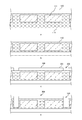
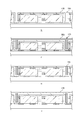
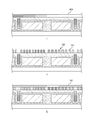
- FIG. 5 to 7 are diagrams showing an example of a method for manufacturing an image sensor according to the first embodiment of the present disclosure.
- 5 to 7 are views showing an example of the manufacturing process of the image pickup device 1.
- a p-type well region is formed on the semiconductor substrate 110.
- An n-type semiconductor region 111 or the like constituting the photoelectric conversion unit 101 is formed in the p-type well region. This can be done, for example, by ion implantation.
- the wiring region 120 is formed on the surface of the semiconductor substrate 110 (A in FIG. 5). This step corresponds to the photoelectric conversion part forming step.
- the top and bottom of the semiconductor substrate 110 is inverted and the back surface side is ground to form the semiconductor substrate 110 to a desired thickness (B in FIG. 5).
- the resist 301 is placed on the back surface of the semiconductor substrate 110.
- the opening 302 is arranged in the region forming the recess 130.
- no opening is formed in the region 309 where the non-separable region 132 is arranged (C in FIG. 5).
- etching is performed using the resist 301 as a mask. The above-mentioned dry etching can be applied to this etching.
- the recess 130 is formed by this etching.
- the region 309 in which the non-separation region 132 is arranged is not etched, and a gap portion of the separation region 131 described in FIG. 2 is formed (D in FIG. 5).
- the resist 301 is removed.
- the step corresponds to the recess forming step.
- the insulating film 140 is formed on the back surface of the semiconductor substrate 110 including the inner wall of the recess 130. This can be done, for example, by CVD (Chemical Vapor Deposition). Before forming the insulating film 140, the fixed charge film may be formed on the back surface of the semiconductor substrate 110 including the inner wall of the recess 130 (E in FIG. 6). Next, the metal film 303 is arranged on the back surface of the semiconductor substrate 110 including the inner wall of the recess 130. This can be done, for example, by forming a W film by CVD. As a result, a metal material can be embedded in the recess 130 (F in FIG. 6).
- CVD Chemical Vapor Deposition
- the back surface of the semiconductor substrate 110 is ground to remove the metal film 303 other than the recess 130.
- This can be done, for example, by chemical mechanical polishing (CMP).
- CMP chemical mechanical polishing
- the separation region 131 can be formed (G in FIG. 6). This step corresponds to the separation region forming step.
- the insulating film 140 is formed again on the back surface of the semiconductor substrate 110 (H in FIG. 6).
- the metal film 304 which is the material of the strip-shaped conductor 151 of the polarizing portion 150 is arranged. This can be done, for example, by sputtering (I in FIG. 7).
- the metal film 304 is etched to form the strip-shaped conductor 151 to form the polarizing portion 150 (J in FIG. 7). The step corresponds to a polarizing portion forming step.
- the insulating film 161 is arranged (K in FIG. 7). After that, the image sensor 1 can be manufactured by forming the protective film 162, the color filter 170, and the on-chip lens 180.
- the configuration of the image sensor 1 is not limited to this example.
- a separation region 131 formed by embedding an insulating member made of SiO 2 and SiN or the like in the recess 130 can also be used. It is also possible to omit the color filter 170 of the pixel 100 and adopt a configuration for generating a monochrome image signal.
- the separation region 131 is arranged between the plurality of pixels 100 including the polarizing unit 150, and the separation region 131 at the corner of the pixel 100
- the non-separable region 132 is formed by the semiconductor substrate 110 in the gap portion.
- Second Embodiment> In the image pickup device 1 of the first embodiment described above, four types of polarizing portions 150 having different polarization directions are arranged on the pixel 100. On the other hand, the image sensor 1 of the second embodiment of the present disclosure is different from the above-described first embodiment in that the types of the polarizing unit 150 arranged in the pixel 100 are reduced.
- FIG. 8 is a diagram showing a configuration example of a separation region according to the second embodiment of the present disclosure. Similar to FIG. 3, FIG. 3 is a plan view of a plurality of pixels 100 arranged in the pixel array unit 10 as viewed from an incident surface. It differs from the pixel array unit 10 described with reference to FIG. 3 in that three types of polarizing units 150 having different polarization directions are arranged on the pixel 100.
- a polarizing portion 150 whose polarization direction is orthogonal to the polarizing portion 150 of the pixel 100a is arranged.
- Polarizing portions 150 in the same polarization direction are arranged in the pixels 100b and the pixels 100c.
- the polarized light unit 150 of the pixel 100b and the pixel 100c is a polarized light unit whose polarization direction is 45 degrees different from that of the respective polarized light unit 150 of the pixel 100a and the pixel 100d.
- the non-separable region 132 is arranged between the pixel 100a and the pixel 100b, the pixel 100b and the pixel 100c, and the pixel 100c and the pixel 100d, respectively.
- the non-separable region 132 is arranged between the pixels 100 in which the polarizing portions 150 in the polarization directions that are not orthogonal to each other are arranged.
- One non-separable region 132 is arranged at the intersection of the boundaries of the pixels 100, and a T-shaped separation region 131 is formed in a plan view.
- the image sensor 1 of the second embodiment of the present disclosure is not affected by the semiconductor substrate 110 in the gap portion of the separation region 131 at the corner of the pixel 100 even when the types of the polarizing portions 150 are reduced.
- a separation region 132 is formed. As a result, it is possible to reduce the depth variation of the recess 130 for arranging the separation region 131, and it is possible to reduce the crosstalk.
- the separation region 131 is arranged on the back surface of the semiconductor substrate 110.
- the image sensor 1 of the third embodiment of the present disclosure is different from the above-described first embodiment in that a separation region 131 penetrating from the back surface to the front surface of the semiconductor substrate 110 is arranged.
- FIG. 9 is a diagram showing a configuration example of pixels according to the third embodiment of the present disclosure. Similar to FIG. 2, FIG. 2 is a schematic cross-sectional view showing a configuration example of the pixel 100. It differs from the pixel 100 described in FIG. 2 in that the separation region 131 penetrates the semiconductor substrate 110.
- the separation region 131 in the figure is arranged in a recess 130 penetrating from the back surface to the front surface of the semiconductor substrate 110, and is configured to penetrate the semiconductor substrate 110. Thereby, the separation ability of the pixel 100 can be improved. Crosstalk can be reduced even when the film thickness of the semiconductor substrate 110 is thin. Even in this case, the depth variation of the recess 130 can be reduced by arranging the non-separable region 132.
- the image sensor 1 of the third embodiment of the present disclosure can further reduce the influence of crosstalk by arranging the separation region 131 penetrating the semiconductor substrate 110.
- the non-separation region 132 is arranged in the gap portion of the separation region 131.
- the image sensor 1 of the fourth embodiment of the present disclosure proposes the size of the gap portion of the separation region 131.
- FIG. 10 is a diagram showing a configuration example of a separation region according to a fourth embodiment of the present disclosure.
- the figure is a plan view seen from the incident surface of the plurality of pixels 100, and is a simplified view of the configurations of the separated region 131 and the non-separated region 132.
- the non-separable region 132 As described above, by arranging the non-separable region 132, the occurrence of the microloading phenomenon can be reduced and the crosstalk can be reduced. On the other hand, by arranging the non-separable region 132, crosstalk occurs through the non-separable region 132.
- the gap G in the gap portion is configured to be approximately 10% or less of the width W1 of the rectangular pixel 100.
- the ratio of the error due to crosstalk caused by the non-separated region 132 to the image signal can be reduced, and the influence of crosstalk via the non-separated region 132 can be reduced while reducing the occurrence of the microloading phenomenon. Can be done.
- the gap G in the gap portion may be configured to have a size substantially equal to the width W2 of the separation region 131.
- the width W2 of the separation region 131 and the gap G of the gap portion can be configured to have a size of 100 nm. Even in this case, the occurrence of the microloading phenomenon can be reduced.
- the image sensor 1 of the fourth embodiment of the present disclosure regulates the size of the gap portion of the separation region 131 in which the non-separation region 132 is arranged. As a result, the influence of crosstalk via the non-separated region 132 can be reduced while reducing the occurrence of the microloading phenomenon.
- the pixel 100 including the polarizing unit 150 is arranged.
- the image sensor 1 of the fifth embodiment of the present disclosure is different from the above-described first embodiment in that pixels not provided with the polarizing unit 150 are further arranged.
- FIG. 11 is a diagram showing a configuration example of a separation region according to a fifth embodiment of the present disclosure. Similar to FIG. 3, FIG. 3 is a plan view of a plurality of pixels 100 arranged in the pixel array unit 10 as viewed from an incident surface. It differs from the pixel array unit 10 described with reference to FIG. 3 in that the pixel 200 not provided with the polarizing unit 150 is arranged.
- the pixel 200 in the figure is a pixel that does not include the polarizing unit 150.
- the pixel 200 is a pixel that generates a normal image signal that does not include polarization information.
- the pixel 200 can be composed of pixels in which the protective film 162 is arranged instead of the polarizing portion 150 in the pixel 100 in FIG.
- the non-separable region 132 can be arranged between the pixels 100 and the pixels 200. Further, also in the image pickup device 1 of the figure, the non-separable region 132 is arranged between the pixels 100 in which the polarizing portions 150 in the non-orthogonal polarization directions are arranged.
- the pixel 200 is an example of the second pixel described in the claims.
- the microloading phenomenon occurs by arranging the non-separable region 132 between the pixels 200 and the pixels 100 which do not have the polarizing unit 150. Can be reduced and crosstalk can be reduced.
- the image pickup device 1 of the first embodiment described above includes pixels 100 having a rectangular shape in a plan view on an incident surface.
- the image sensor 1 of the sixth embodiment of the present disclosure is different from the above-described first embodiment in that it includes pixels 100 having a shape other than a rectangle.
- FIG. 12 is a diagram showing a configuration example of a separation region according to a sixth embodiment of the present disclosure. Similar to FIG. 3, FIG. 3 is a plan view of a plurality of pixels 100 arranged in the pixel array unit 10 as viewed from an incident surface. It differs from the pixel array unit 10 described with reference to FIG. 3 in that it includes pixels 100 having a hexagonal shape.
- the pixels 100a, 100b, 100c, and 100d in the figure are formed in a hexagonal shape in a plan view of the incident surface. Similar to FIG. 3, each of the pixel 100a, the pixel 100b, the pixel 100c, and the pixel 100d is provided with a polarizing portion 150 having different polarization directions by 45 degrees. A separation region 131 is arranged between the pixels 100a and the like. Further, the pixel array unit 10 is further arranged with a non-separable region 132 formed of a semiconductor substrate 110 in the gap portion of the separation region 131 near the corner of the pixel 100a or the like.
- the non-separable region 132 is arranged between the pixels 100a and the like provided with the polarizing portions 150 in the polarization directions that are not orthogonal to each other. Similar to FIG. 3, it is arranged between the pixels 100a and 100b, between the pixels 100b and 100c, between the pixels 100c and 100d, and between the pixels 100d and 100a in the same figure.
- the configuration of the image sensor 1 is not limited to this example. For example, it is possible to arrange the pixels 100 having another polygonal shape.
- the image sensor 1 of the fifth embodiment of the present disclosure includes the hexagonal pixel 100
- the non-separable region 132 is arranged between the pixels 100 to cause microloading.
- the occurrence of the phenomenon can be reduced and crosstalk can be reduced.
- the technology according to the present disclosure can be applied to various products.
- the present technology may be realized as an image pickup device mounted on an image pickup device such as a camera.
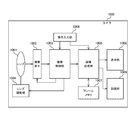
- FIG. 13 is a block diagram showing a schematic configuration example of a camera which is an example of an imaging device to which the present technology can be applied.
- the camera 1000 in the figure includes a lens 1001, an image pickup element 1002, an image pickup control unit 1003, a lens drive unit 1004, an image processing unit 1005, an operation input unit 1006, a frame memory 1007, a display unit 1008, and the like.
- a recording unit 1009 is provided.
- the lens 1001 is a photographing lens of the camera 1000.
- the lens 1001 collects light from the subject and causes the light to be incident on the image pickup device 1002 described later to form an image of the subject.
- the image sensor 1002 is a semiconductor element that captures light from a subject focused by the lens 1001.
- the image sensor 1002 generates an analog image signal according to the irradiated light, converts it into a digital image signal, and outputs the signal.
- the image pickup control unit 1003 controls the image pickup in the image pickup device 1002.
- the image pickup control unit 1003 controls the image pickup device 1002 by generating a control signal and outputting the control signal to the image pickup device 1002. Further, the image pickup control unit 1003 can perform autofocus on the camera 1000 based on the image signal output from the image pickup device 1002.
- the autofocus is a system that detects the focal position of the lens 1001 and automatically adjusts it.
- a method (image plane phase difference autofocus) in which the image plane phase difference is detected by the phase difference pixels arranged in the image sensor 1002 to detect the focal position can be used. It is also possible to apply a method (contrast autofocus) of detecting the position where the contrast of the image is highest as the focal position.
- the image pickup control unit 1003 adjusts the position of the lens 1001 via the lens drive unit 1004 based on the detected focal position, and performs autofocus.
- the image pickup control unit 1003 can be configured by, for example, a DSP (Digital Signal Processor) equipped with firmware.
- DSP Digital Signal Processor
- the lens driving unit 1004 drives the lens 1001 based on the control of the imaging control unit 1003.
- the lens driving unit 1004 can drive the lens 1001 by changing the position of the lens 1001 using a built-in motor.
- the image processing unit 1005 processes the image signal generated by the image sensor 1002. This processing includes, for example, demosaic to generate an image signal of a color that is insufficient among the image signals corresponding to red, green, and blue for each pixel, noise reduction to remove noise of the image signal, and coding of the image signal. Applicable.
- the image processing unit 1005 can be configured by, for example, a microcomputer equipped with firmware.
- the operation input unit 1006 receives the operation input from the user of the camera 1000.
- a push button or a touch panel can be used for the operation input unit 1006.
- the operation input received by the operation input unit 1006 is transmitted to the image pickup control unit 1003 and the image processing unit 1005. After that, processing according to the operation input, for example, processing such as imaging of the subject is activated.
- the frame memory 1007 is a memory that stores a frame that is an image signal for one screen.
- the frame memory 1007 is controlled by the image processing unit 1005 and holds the frame in the process of image processing.
- the display unit 1008 displays the image processed by the image processing unit 1005.
- a liquid crystal panel can be used.
- the recording unit 1009 records the image processed by the image processing unit 1005.
- a memory card or a hard disk can be used for the recording unit 1009.
- the cameras to which this disclosure can be applied have been described above.
- the present technology can be applied to the image pickup device 1002 among the configurations described above.
- the image pickup device 1 described with reference to FIG. 1 can be applied to the image pickup device 1002.
- the image processing unit 1005 is an example of the processing circuit described in the claims.
- the camera 1000 is an example of the image pickup apparatus described in the claims.
- the technology according to the present disclosure may be applied to other devices such as a monitoring device.
- the present disclosure can be applied to a semiconductor device in the form of a semiconductor module in addition to an electronic device such as a camera.
- the technique according to the present disclosure can be applied to an image pickup module which is a semiconductor module in which the image pickup element 1002 and the image pickup control unit 1003 of FIG. 13 are enclosed in one package.
- drawings in the above-described embodiment are schematic, and the ratio of the dimensions of each part does not always match the actual one.
- the drawings include parts having different dimensional relationships and ratios from each other.
- the present technology can have the following configurations.
- a plurality of pixels including a polarizing unit that polarizes incident light in a specific polarization direction and a photoelectric conversion unit formed on a semiconductor substrate that performs photoelectric conversion of the polarized incident light.
- a separation region arranged on the semiconductor substrate and separating the plurality of pixels from each other,
- An image pickup device including a non-separable region formed of the semiconductor substrate in a gap portion formed in the separated region near the corner of the pixel.
- the polarizing portion is composed of a wire grid composed of a plurality of strip-shaped conductors arranged at a predetermined pitch.
- the non-separable region is arranged between the plurality of pixels having polarizing portions in the specific polarization direction that are not orthogonal to each other.
- the separation region is formed in a recess formed in the semiconductor substrate.
- the separation region has a member that blocks the incident light.
- any of the above (1) to (8), wherein the non-separable region is composed of the semiconductor substrate in the gap portion of the gap of approximately 10% of the width of the surface of the pixel irradiated with the incident light.
- the image sensor described in Crab is any of the above (1) to (8), wherein the non-separable region is composed of the semiconductor substrate in the gap portion having a gap substantially equal to the width of the surface irradiated with the incident light in the separated region.
- the image pickup device according to any one of (1) to (10), further comprising a second pixel which is the pixel not provided with the polarizing portion. (12) The image pickup device according to (11), wherein the non-separable region is arranged between the pixel and the second pixel. (13) A plurality of pixels including a polarizing unit that polarizes incident light in a specific polarization direction and a photoelectric conversion unit formed on a semiconductor substrate that performs photoelectric conversion of the polarized incident light.
- An image pickup apparatus including a processing circuit for processing an image signal generated based on the photoelectric conversion.
- Image sensor 10 Pixel array unit 30
- Photoelectric conversion unit 110 Semiconductor substrate 130 Recessed 131 Separation area 132 Non-separation area 150
- Polarizing part 151 Band-shaped conductor 1000 Camera 1002 Imaging Element 1005 Image processing unit
Landscapes
- Engineering & Computer Science (AREA)
- Multimedia (AREA)
- Signal Processing (AREA)
- Physics & Mathematics (AREA)
- General Physics & Mathematics (AREA)
- Optics & Photonics (AREA)
- Solid State Image Pick-Up Elements (AREA)
- Polarising Elements (AREA)
- Transforming Light Signals Into Electric Signals (AREA)
Abstract
被写体の偏光情報を取得する撮像素子における隣接する画素の間のクロストークを低減する。 撮像素子は、複数の画素と分離領域と非分離領域とを具備する。その複数の画素は、入射光を特定の偏光方向に偏光する偏光部および半導体基板に形成されて偏光された入射光の光電変換を行う光電変換部をそれぞれ備える。その分離領域は、半導体基板に配置されて複数の画素同士を分離する。その非分離領域は、画素の隅部の近傍の分離領域に形成される間隙部分の半導体基板により構成される。
Description
本開示は、撮像素子および撮像装置に関する。詳しくは、被写体の偏光情報を取得する撮像素子および当該撮像素子を使用する撮像装置に関する。
従来、被写体の偏光情報を取得する撮像素子が使用されている。偏光情報を取得することにより、特定の偏光方向の入射光、例えば、水溜まりやガラス面からの反射光等を検出し、この特定の偏光方向の入射光を除去することができる。撮像素子により撮像される画像の画質を向上させることが可能となる。また、偏光情報を用いて被写体の表面の3次元形状を取得することもできる。偏光情報は、特定の偏光方向の入射光を透過する偏光部を撮像素子の画素に配置することにより、取得することができる。この偏光部としてワイヤグリッドにより構成された偏光部を使用することができる。このワイヤグリッドは、複数の帯状の導体が所定のピッチに基づいて配列されて構成されたものである。複数の帯状の導体の並び方向に平行な偏光方向の入射光がワイヤグリッドによる偏光部を透過し、複数の帯状の導体の並び方向に垂直な偏光方向の入射光は偏光部により反射されて減衰される。
このような撮像素子として、例えば、画素毎の光電変換素子が配置された半導体基板における光電変換素子の周囲を囲む遮光膜を備え、半導体基板の裏面に偏光部が配置された撮像素子が使用されている(例えば、特許文献1参照。)。この撮像素子においては、遮光膜は隣接する画素間を埋めるように格子状に配置される。また、遮光膜は導電遮光材料により構成されて偏光部を構成する帯状の導体に接続され、遮光膜を介して偏光部に負のバイアス電圧が印加される。このバイアス電圧により半導体基板の裏面に負の電位が与えられて半導体基板の裏面側のピニングが強化される。
上述の従来技術では、画素間のクロストークが増加するという問題がある。上述の遮光膜は、エッチングにより半導体基板に格子状の溝を形成し、この溝に金属等の導電遮光材料を埋め込むことにより形成される。この溝を形成する際、格子を構成する縦横の溝の交点の部分においてマイクロローディング現象を生じて溝が深くなる。このため、交点以外の溝が相対的に浅くなり、形成後の遮光膜の深さが不足する。この深さが不足する遮光膜の領域において、隣接する画素への入射光の漏洩を生じてクロストークが増加するという問題がある。このクロストークにより偏光情報の誤差が増加し、撮像素子により撮像される画像の画質が低下する。
本開示は、上述した問題点に鑑みてなされたものであり、被写体の偏光情報を取得する撮像素子における隣接する画素の間のクロストークを低減することを目的としている。
本開示は、上述の問題点を解消するためになされたものであり、その第1の態様は、入射光を特定の偏光方向に偏光する偏光部および半導体基板に形成されて上記偏光された入射光の光電変換を行う光電変換部を備える複数の画素と、上記半導体基板に配置されて上記複数の画素同士を分離する分離領域と、上記画素の隅部の近傍の上記分離領域に形成される間隙部分の上記半導体基板により構成される非分離領域とを具備する撮像素子である。
また、この第1の態様において、上記偏光部は、上記入射光のうち特定の偏光方向の入射光を透過することにより上記入射光を偏光してもよい。
また、この第1の態様において、上記偏光部は、所定のピッチに配列された複数の帯状導体からなるワイヤグリッドにより構成されてもよい。
また、この第1の態様において、上記非分離領域は、互いに直交しない上記特定の偏光方向の偏光部を備える上記複数の画素同士の間に配置されてもよい。
また、この第1の態様において、上記分離領域は、上記半導体基板に形成された凹部に形成されてもよい。
また、この第1の態様において、上記分離領域は、上記入射光を遮光する部材を有してもよい。
また、この第1の態様において、上記分離領域は、金属により構成される部材を有してもよい。
また、この第1の態様において、上記分離領域は、絶縁部材を有してもよい。
また、この第1の態様において、上記非分離領域は、上記画素の上記入射光が照射される面の幅の略10%の隙間の上記間隙部分の上記半導体基板により構成されてもよい。
また、この第1の態様において、上記非分離領域は、上記分離領域の上記入射光が照射される面の幅と略等しい隙間の上記間隙部分の上記半導体基板により構成されてもよい。
また、この第1の態様において、上記偏光部を備えない上記画素である第2の画素をさらに具備してもよい。
また、この第1の態様において、上記非分離領域は、上記画素および上記第2の画素の間に配置されてもよい。
また、本開示の第2の態様は、入射光を特定の偏光方向に偏光する偏光部および半導体基板に形成されて上記偏光された入射光の光電変換を行う光電変換部を備える複数の画素と、上記半導体基板に配置されて上記複数の画素同士を分離する分離領域と、上記画素の隅部の近傍の上記分離領域に形成される間隙部分の上記半導体基板により構成される非分離領域と、上記光電変換に基づいて生成される画像信号を処理する処理回路とを具備する撮像装置である。
本開示の態様により、画素の境界が交差する領域の分離領域に隣接して非分離領域が配置されるという作用をもたらす。
次に、図面を参照して、本開示を実施するための形態(以下、実施の形態と称する)を説明する。以下の図面において、同一または類似の部分には同一または類似の符号を付している。また、以下の順序で実施の形態の説明を行う。
1.第1の実施の形態
2.第2の実施の形態
3.第3の実施の形態
4.第4の実施の形態
5.第5の実施の形態
6.第6の実施の形態
7.カメラへの応用例
1.第1の実施の形態
2.第2の実施の形態
3.第3の実施の形態
4.第4の実施の形態
5.第5の実施の形態
6.第6の実施の形態
7.カメラへの応用例
<1.第1の実施の形態>
[撮像素子の構成]
図1は、本開示の実施の形態に係る撮像素子の構成例を示す図である。同図の撮像素子1は、画素アレイ部10と、垂直駆動部20と、カラム信号処理部30と、制御部40とを備える。
[撮像素子の構成]
図1は、本開示の実施の形態に係る撮像素子の構成例を示す図である。同図の撮像素子1は、画素アレイ部10と、垂直駆動部20と、カラム信号処理部30と、制御部40とを備える。
画素アレイ部10は、画素100が2次元格子状に配置されて構成されたものである。ここで、画素100は、照射された光に応じた画像信号を生成するものである。この画素100は、照射された光に応じた電荷を生成する光電変換部を有する。また画素100は、画素回路をさらに有する。この画素回路は、光電変換部により生成された電荷に基づく画像信号を生成する。画像信号の生成は、後述する垂直駆動部20により生成された制御信号により制御される。画素アレイ部10には、信号線11および12がXYマトリクス状に配置される。信号線11は、画素100における画素回路の制御信号を伝達する信号線であり、画素アレイ部10の行毎に配置され、各行に配置される画素100に対して共通に配線される。信号線12は、画素100の画素回路により生成された画像信号を伝達する信号線であり、画素アレイ部10の列毎に配置され、各列に配置される画素100に対して共通に配線される。これら光電変換部および画素回路は、半導体基板に形成される。
垂直駆動部20は、画素100の画素回路の制御信号を生成するものである。この垂直駆動部20は、生成した制御信号を同図の信号線11を介して画素100に伝達する。カラム信号処理部30は、画素100により生成された画像信号を処理するものである。このカラム信号処理部30は、同図の信号線12を介して画素100から伝達された画像信号の処理を行う。カラム信号処理部30における処理には、例えば、画素100において生成されたアナログの画像信号をデジタルの画像信号に変換するアナログデジタル変換が該当する。カラム信号処理部30により処理された画像信号は、撮像素子1の画像信号として出力される。制御部40は、撮像素子1の全体を制御するものである。この制御部40は、垂直駆動部20およびカラム信号処理部30を制御する制御信号を生成して出力することにより、撮像素子1の制御を行う。制御部40により生成された制御信号は、信号線41および42により垂直駆動部20およびカラム信号処理部30に対してそれぞれ伝達される。なお、カラム信号処理部30は、請求の範囲に記載の処理回路の一例である。
[画素の構成]
図2は、本開示の第1の実施の形態に係る画素の構成例を示す図である。同図は、画素100の構成例を表す模式断面図である。同図の画素100は、半導体基板110と、配線領域120と、分離領域131と、非分離領域132と、絶縁膜140および161と、偏光部150と、保護膜162と、カラーフィルタ170と、オンチップレンズ180とを備える。
図2は、本開示の第1の実施の形態に係る画素の構成例を示す図である。同図は、画素100の構成例を表す模式断面図である。同図の画素100は、半導体基板110と、配線領域120と、分離領域131と、非分離領域132と、絶縁膜140および161と、偏光部150と、保護膜162と、カラーフィルタ170と、オンチップレンズ180とを備える。
半導体基板110は、光電変換部や画素回路等の素子の拡散領域が形成される半導体の基板である。この半導体基板110には、例えば、シリコン(Si)により構成された半導体基板を使用することができる。光電変換部や画素回路の素子の拡散領域は、半導体基板110に形成されたウェル領域に形成される。便宜上、同図の半導体基板110は、p型のウェル領域に構成されるものと想定する。このp型のウェル領域にn型の半導体領域を配置することにより光電変換部や画素回路の素子の拡散領域を形成することができる。
同図には、これらの例として、光電変換部101を記載した。この光電変換部101は、同図の半導体基板110に配置されたn型の半導体領域111により構成される。具体的には、n型の半導体領域111と周囲のp型のウェル領域との界面のpn接合によるフォトダイオードが光電変換部101に該当する。このpn接合部分に入射光が照射されると、光電変換による電荷が生成される。この電荷のうちの電子がn型の半導体領域111に蓄積される。この蓄積された電荷(電子)に基づいて、不図示の画素回路により画像信号が生成される。
配線領域120は、半導体基板110の表面に隣接して配置され、画素100の画素回路の素子等に信号を伝達する配線が形成される領域である。同図の配線領域120は、配線層122および絶縁層121により構成される。配線層122は、信号を伝達する配線である。この配線層122は、例えば、銅(Cu)等の金属により構成することができる。絶縁層121は、配線層122を絶縁するものである。この絶縁層121は、例えば、酸化シリコン(SiO2)や窒化シリコン(SiN)により構成することができる。
絶縁膜140は、半導体基板110の裏面に隣接して配置され、半導体基板110の裏面を保護する膜である。この絶縁膜140は、例えば、SiO2やSiNより構成することができる。なお、半導体基板110および絶縁膜140の間に半導体基板110の界面準位をピニングする固定電荷膜を配置することもできる。固定電荷膜には、例えば、酸化ハフニウム(HfO2)の膜を使用することができる。
偏光部150は、絶縁膜140の表面に配置されて被写体からの入射光を特定の偏光方向に偏光するものである。この偏光部150には、例えば、特定の偏光方向の入射光を透過させることにより入射光の偏光を行う偏光部を使用することができる。同図の偏光部150は、ワイヤグリッドにより構成される偏光部の例を表したものである。このワイヤグリッドは、複数の帯状の導体が所定のピッチに配列されて構成された偏光部である。同図の偏光部150は、帯状導体151が配列されて構成される。複数の帯状導体151の間の領域152には、空気等の誘電体を配置することができる。
帯状導体151の並び方向に垂直な偏光方向、すなわち帯状導体151に平行な偏光方向の入射光は偏光部150により減衰される。入射光により帯状導体151の内部の電荷が振動して反射光を生じるためである。一方、帯状導体151の並び方向に平行な偏光方向、すなわち帯状導体151に垂直な偏光方向の入射光は、偏光部150を透過する。帯状導体151内部の電荷の振動が制限されるためである。偏光部150を透過する偏光方向は、透過軸と称される。
また、偏光部150の透過光のうち最大の透過光と最小の透過光との比率は、消光比と称される。前述のように、偏光部150は、特定の偏光方向(透過軸)の光を透過する。一方、偏光部150は、透過軸とは異なる偏光方向の光を減衰する。透過軸に対して90度異なる偏光方向の透過光が最大の減衰量となる。このような透過光の最大値および最小値の比率が消光比となる。消光比が高いほど、ノイズの少ない偏光情報を取得することができる。なお、後述する分離領域131が配置される半導体基板110の裏面に隣接して偏光部150を配置することにより、クロストークを低減することができる。同図の偏光部150は、絶縁膜140を介して半導体基板110の裏面に隣接して配置される。
絶縁膜161は、偏光部150を絶縁する膜である。また、絶縁膜161は、偏光部150の帯状導体151の保護をさらに行う。この絶縁膜161は、例えば、SiO2により構成することができる。
保護膜162は、半導体基板110の裏面を保護するとともに平坦化する膜である。保護膜162を配置することにより、後述するカラーフィルタ170が配置される面が平坦化され、色むらの発生を防ぐことができる。
カラーフィルタ170は、入射光のうち所定の波長の光を透過させる光学的なフィルタである。カラーフィルタ170を配置することにより、カラーの画像信号を生成することができる。カラーフィルタ170として、例えば、赤色光、緑色光および青色光を透過するカラーフィルタを使用することができる。
オンチップレンズ180は、画素100毎に配置されて入射光を集光するレンズである。このオンチップレンズ180は、半球形状に構成されて入射光を光電変換部101(n型の半導体領域111)に集光する。オンチップレンズ180は、例えば、アクリル樹脂等の有機材料やSiN等の無機材料により構成することができる。
同図の画素100は、オンチップレンズ180により集光され、カラーフィルタ170および偏光部150を透過した入射光が半導体基板110の裏面から光電変換部101に照射される。このような半導体基板110の裏面に入射光が照射される撮像素子1は、裏面照射型の撮像素子と称される。ここで、撮像素子1の入射光が照射される面を入射面と称する。
半導体基板110における画素100の境界には、分離領域131が配置される。この分離領域131は、画素100の半導体基板110を囲繞する形状に構成され、画素100を分離するものである。分離領域131を配置することにより、隣接する画素100との間の電荷の移動を防ぐことができ、クロストークを低減することができる。ここでクロストークとは、隣接する画素100の影響を受けて画像信号が変化することであり、画像信号のノイズの原因となるものである。同図の分離領域131は、例えば、半導体基板110に形成された溝状の凹部130に分離用の部材を埋め込むことにより構成することができる。同図の分離領域131は、半導体基板110の入射面である裏面における画素100を分離し、半導体基板110の裏面から表面に達しない深さに形成される例を表したものである。
また、分離用の部材として入射光を遮光する部材を使用すると好適である。隣接する画素100の入射光の漏洩を防止し、クロストークをさらに低減することができるためである。具体的には、隣接する画素100における異なる波長に対応するカラーフィルタ170を透過した光の入射を防ぐことにより、混色の発生を防止することができる。ここで、混色とは、異なる色の画像信号が混入する現象であり、クロストークの一例である。また、入射光を遮光する部材による分離領域131を配置することにより、隣接する画素100における偏光部150により異なる方向に偏光された入射光の入射を防ぐことができる。前述の消光比の低下を防止することができる。
入射光を遮光する部材には、例えば、タングステン(W)、アルミニウム(Al)および銅(Cu)等の金属材料を使用することができる。同図の分離領域131は、半導体基板110における画素100の境界部分に形成された凹部130の内壁に絶縁膜を配置し、上述の金属材料であるWを埋め込むことにより形成されたものである。
画素100の境界の半導体基板110には、非分離領域132がさらに配置される。この非分離領域132は、上述の分離領域131の間隙部分の半導体基板110により構成される。同図の半導体基板110の破線の矩形は非分離領域132を表したものである。この分離領域131の間隙部分は、画素100の隅部の近傍に配置される。分離領域131および非分離領域132の構成の詳細については後述する。
[分離領域の構成]
図3は、本開示の第1の実施の形態に係る分離領域の構成例を示す図である。同図は、画素アレイ部10に配置される複数の画素100の入射面からみた平面図であり、分離領域131および非分離領域132の構成例を表す平面図である。同図においてハッチングが付された領域は、半導体基板110の裏面を表す。また、二点鎖線の矩形は、画素100を表す。また、白抜きの矩形は分離領域131を表す。また、破線の矩形は、偏光部150の帯状導体151を表す。なお、図2は、同図のa-a’線に沿った断面の構成を表したものである。
図3は、本開示の第1の実施の形態に係る分離領域の構成例を示す図である。同図は、画素アレイ部10に配置される複数の画素100の入射面からみた平面図であり、分離領域131および非分離領域132の構成例を表す平面図である。同図においてハッチングが付された領域は、半導体基板110の裏面を表す。また、二点鎖線の矩形は、画素100を表す。また、白抜きの矩形は分離領域131を表す。また、破線の矩形は、偏光部150の帯状導体151を表す。なお、図2は、同図のa-a’線に沿った断面の構成を表したものである。
同図は、平面視において矩形形状に構成される画素100の例を表したものである。また、同図の2行2列に配置された画素100a、100b、100cおよび100dには、それぞれ異なる偏光方向に入射光を偏光する偏光部150が配置される。すなわち、画素100a、100b、100cおよび100dには、透過軸が45度ずつ異なる偏光部150が配置される。この2行2列の画素100により、4つの偏光方向の入射光を検出し、4方向の偏光情報を含む画像信号を生成することができる。
分離領域131は、画素100同士の境界に配置され、画素100の周囲を囲繞する形状に配置される。一方、非分離領域132は、矩形形状の画素100の隅部の近傍に形成される分離領域131の間隙部分に配置される。この間隙は、平面視において格子形状に配置される縦横の分離領域131の交点に隣接する分離領域131に形成される。同図に表したように、分離領域131は、平面視における格子形状の画素100の境界が交わる交点において縦または横方向の一方が貫通するとともに他方が非分離領域132の間隙部分により分断される形状に構成される。また、全ての画素100の境界の交点に隣接して非分離領域132が配置される。
前述のように、分離領域131は、半導体基板110に形成された凹部130に配置される。この凹部130は、半導体基板110の裏面をエッチングすることにより形成することができる。この凹部130をエッチングにより形成する際、非分離領域132を配置することにより、凹部130の深さばらつきを低減することができる。これにより、深さばらつきに基づくクロストークの発生を低減することができる。凹部130の深さばらつきの詳細については後述する。
なお、非分離領域132は、画素100に配置される偏光部150の偏光方向が互いに直交しない画素100の間に配置することができる。具体的には、同図の画素100aおよび画素100bの間、画素100bおよび画素100cの間、画素100cおよび画素100dの間ならびに画素100dおよび画素100aの間に配置される。
この非分離領域132を配置することにより、隣接する画素100の間の入射光の漏洩を生じる。異なる偏光方向の偏光部150を透過した入射光が漏洩することとなり、消光比が低下する。しかし、分離領域131は、偏光方向が直交しない偏光部150が配置される画素100の間に配置される。このため、消光比の低下を軽減することができる。これを画素100aおよび画素100bを例に挙げて説明する。画素100aおよび画素100bの間には、非分離領域132が配置される。画素100aの偏光部150の透過軸に対して画素100bの偏光部150は45度ずれた偏光方向に構成される。偏光部150の透過軸に対して45度ずれた偏光方向の入射光は、略50%の光量に減衰されて透過する。すなわち、非分離領域132を介して画素100aに混入する画素100bの偏光部150を透過した入射光は、画素100aの偏光部150において略50%に減衰された偏光方向の入射光である。このため、非分離領域132を配置した場合であっても、軽微な消光比の増加にとどめることができる。
一方、偏光方向が略直交する偏光部150を備える画素100同士の間には非分離領域132を配置しない。例えば、偏光方向が80乃至100度異なる画素100同士の間には非分離領域132を配置しない構成を採ることができる。同図においては、画素100aおよび画素100cの間ならびに画素100bおよび画素100dの間には、非分離領域132は配置されない。偏光部150は、自身の透過軸に対して直交する偏光方向の入射光を略100%遮光する。このため、直交する偏光方向の偏光部150が配置された画素100からの入射光の混入を生じると消光比が大幅に低下することとなる。この直交する偏光方向の偏光部150が配置された画素100の間には非分離領域132を配置しないことにより、非分離領域132を介した入射光の混入を防ぐことができる。直交する偏光方向の偏光部150が配置された画素100に基づく消光比の低下を防止することが可能となる。なお、偏光方向の略直交する場合には、偏光方向が80乃至100度異なる場合を想定する。
このように、直交しない偏光方向の偏光部150が配置される画素100の間に非分離領域132を配置することにより、非分離領域132に起因する消光比の低下を軽減することができる。
[分離領域の凹部の構成]
図4は、本開示の第1の実施の形態に係る分離領域の凹部の一例を示す図である。同図は、凹部130の形状の一例を示す図であり、非分離領域132の効果を説明する図である。同図におけるAおよびCは、画素100の半導体基板110および分離領域131の簡略化した平面図である。同図におけるBおよびDは、それぞれ同図におけるAおよびCのa-a’線に沿った断面図である。なお、同図に於けるAおよびBは、非分離領域132を配置しない場合の例を比較のために表した図である。
図4は、本開示の第1の実施の形態に係る分離領域の凹部の一例を示す図である。同図は、凹部130の形状の一例を示す図であり、非分離領域132の効果を説明する図である。同図におけるAおよびCは、画素100の半導体基板110および分離領域131の簡略化した平面図である。同図におけるBおよびDは、それぞれ同図におけるAおよびCのa-a’線に沿った断面図である。なお、同図に於けるAおよびBは、非分離領域132を配置しない場合の例を比較のために表した図である。
同図におけるAの画素アレイ部10は、非分離領域132が配置されないため、分離領域131の凹部130が平面視において縦横に交差した形状となる。凹部130は、半導体基板110の裏面を、例えば、エッチングすることにより形成することができる。このエッチングには、異方性のドライエッチングを適用することができる。この異方性のドライエッチングにより高いアスペクト比の溝形状の凹部130を形成することができる。このドライエッチングは、イオン化されたエッチングガスにより半導体基板110をエッチングする方式であり、エッチングガスを半導体基板110の表面に供給しながらエッチングを行う。このエッチングの際、平面視において交差する部分は、線形状の部分と比較して面積が広くなるため、エッチングガスの供給量が多くなり、エッチング速度が増加する。このように、エッチング対象の開口部の面積差に基づいてエッチング速度が変化する現象は、マイクロローディング現象と称される。このマイクロローディング現象により、交差する部分は、他の部分より深い形状の凹部130となる。
同図におけるBは、この様子を表したものである。凹部130の交差する部分と他の部分とはΔdの深さばらつきを生じる。画素100の隅部以外の境界の半導体基板110はΔdだけ分離領域131が浅くなるため、当該領域を介した隣接画素100からのクロストークが大きくなる。赤色光や赤外光等の長波長の入射光は半導体基板110の深部に到達するため、赤色光等の長波長の入射光を透過するカラーフィルタ170が配置される画素100において、クロストークがさらに大きくなる。
これに対し、同図におけるCに表したように、非分離領域132を配置して間隙部分を分離領域131に配置することにより、上述の交差する部分の面積の増加を防ぐことができる。マイクロローディング現象の発生を防止することができ、均一な深さの凹部130を形成することができる。
[画素の製造方法]
図5乃至7は、本開示の第1の実施の形態に係る撮像素子の製造方法の一例を示す図である。図5乃至7は、撮像素子1の製造工程の一例を表した図である。まず、半導体基板110にp型のウェル領域を形成する。このp型のウェル領域に光電変換部101を構成するn型の半導体領域111等を形成する。これは、例えば、イオン注入により行うことができる。次に、半導体基板110の表面に配線領域120を形成する(図5におけるA)。当該工程は、光電変換部形成工程に該当する。次に、半導体基板110の天地を反転させて裏面側を研削し、半導体基板110を所望の厚さに構成する(図5におけるB)。
図5乃至7は、本開示の第1の実施の形態に係る撮像素子の製造方法の一例を示す図である。図5乃至7は、撮像素子1の製造工程の一例を表した図である。まず、半導体基板110にp型のウェル領域を形成する。このp型のウェル領域に光電変換部101を構成するn型の半導体領域111等を形成する。これは、例えば、イオン注入により行うことができる。次に、半導体基板110の表面に配線領域120を形成する(図5におけるA)。当該工程は、光電変換部形成工程に該当する。次に、半導体基板110の天地を反転させて裏面側を研削し、半導体基板110を所望の厚さに構成する(図5におけるB)。
次に、半導体基板110の裏面にレジスト301を配置する。このレジスト301には、凹部130を形成する領域に開口部302が配置される。一方、非分離領域132が配置される領域309には開口部は形成されない(図5におけるC)。次に、レジスト301をマスクとしてエッチングを行う。このエッチングには、前述のドライエッチングを適用することができる。このエッチングにより凹部130を形成する。なお、非分離領域132が配置される領域309はエッチングされず、図2において説明した分離領域131の間隙部分が形成される(図5におけるD)。その後、レジスト301を除去する。当該工程は、凹部形成工程に該当する。
次に、凹部130の内壁を含む半導体基板110の裏面に絶縁膜140を形成する。これは、例えば、CVD(Chemical Vapor Deposition)により行うことができる。なお、絶縁膜140を形成する前に、固定電荷膜を凹部130の内壁を含む半導体基板110の裏面に形成することもできる(図6におけるE)。次に、凹部130の内壁を含む半導体基板110の裏面に金属膜303を配置する。これは、例えば、Wの膜をCVDにより形成することにより行うことができる。これにより、凹部130に金属材料を埋め込むことができる(図6におけるF)。次に、半導体基板110の裏面を研削して凹部130以外の金属膜303を除去する。これは、例えば、化学的機械的研磨(CMP:Chemical Mechanical Polishing)により行うことができる。これにより、分離領域131を形成することができる(図6におけるG)。当該工程は、分離領域形成工程に該当する。
次に、半導体基板110の裏面に絶縁膜140を再度形成する(図6におけるH)。次に、偏光部150の帯状導体151の材料となる金属膜304を配置する。これは、例えばスパッタリングにより行うことができる(図7におけるI)。次に、金属膜304をエッチングして帯状導体151を形成し、偏光部150を形成する(図7におけるJ)。当該工程は、偏光部形成工程に該当する。
次に、絶縁膜161を配置する(図7におけるK)。その後、保護膜162、カラーフィルタ170およびオンチップレンズ180を形成することにより、撮像素子1を製造することができる。
なお、撮像素子1の構成は、この例に限定されない。例えば、凹部130にSiO2およびSiN等による絶縁部材を埋め込んで構成された分離領域131を使用することもできる。また、画素100のカラーフィルタ170を省略し、モノクロの画像信号を生成する構成を採ることもできる。
以上説明したように、本開示の第1の実施の形態の撮像素子1は、偏光部150を備える複数の画素100の間に分離領域131を配置するとともに画素100の隅部の分離領域131の間隙部分の半導体基板110により非分離領域132を形成する。これにより、分離領域131を配置するための凹部130の深さばらつきを低減することができ、クロストークを低減することができる。
<2.第2の実施の形態>
上述の第1の実施の形態の撮像素子1は、偏光方向が異なる4種類の偏光部150が画素100に配置されていた。これに対し、本開示の第2の実施の形態の撮像素子1は、画素100に配置する偏光部150の種類を削減する点で、上述の第1の実施の形態と異なる。
上述の第1の実施の形態の撮像素子1は、偏光方向が異なる4種類の偏光部150が画素100に配置されていた。これに対し、本開示の第2の実施の形態の撮像素子1は、画素100に配置する偏光部150の種類を削減する点で、上述の第1の実施の形態と異なる。
[分離領域の構成]
図8は、本開示の第2の実施の形態に係る分離領域の構成例を示す図である。同図は、図3と同様に、画素アレイ部10に配置される複数の画素100における入射面からみた平面図である。偏光方向が異なる3種類の偏光部150が画素100に配置される点で、図3において説明した画素アレイ部10と異なる。
図8は、本開示の第2の実施の形態に係る分離領域の構成例を示す図である。同図は、図3と同様に、画素アレイ部10に配置される複数の画素100における入射面からみた平面図である。偏光方向が異なる3種類の偏光部150が画素100に配置される点で、図3において説明した画素アレイ部10と異なる。
同図の画素100dには、画素100aの偏光部150とは偏光方向が直交する偏光部150が配置される。画素100bおよび画素100cには、同じ偏光方向の偏光部150が配置される。この画素100bおよび画素100cの偏光部150は、画素100aおよび画素100dのそれぞれの偏光部150と偏光方向が45度異なる偏光部である。非分離領域132は、画素100aおよび画素100b、画素100bおよび画素100cならびに画素100cおよび画素100dの間にそれぞれ配置される。このように、非分離領域132は、互いに直交しない偏光方向の偏光部150が配置される画素100の間に配置される。画素100の境界の交点には、1つの非分離領域132が配置され、平面視においてT字状の分離領域131が形成される。この非分離領域132が配置されることにより、マイクロローディング現象の発生を軽減することができる。
これ以外の撮像素子1の構成は本開示の第1の実施の形態において説明した撮像素子1の構成と同様であるため、説明を省略する。
以上説明したように、本開示の第2の実施の形態の撮像素子1は、偏光部150の種類を削減する場合においても画素100の隅部の分離領域131の間隙部分の半導体基板110により非分離領域132を形成する。これにより、分離領域131を配置するための凹部130の深さばらつきを低減することができ、クロストークを低減することができる。
<3.第3の実施の形態>
上述の第1の実施の形態の撮像素子1は、半導体基板110の裏面に分離領域131が配置されていた。これに対し、本開示の第3の実施の形態の撮像素子1は、半導体基板110の裏面から表面に貫通する分離領域131を配置する点で、上述の第1の実施の形態と異なる。
上述の第1の実施の形態の撮像素子1は、半導体基板110の裏面に分離領域131が配置されていた。これに対し、本開示の第3の実施の形態の撮像素子1は、半導体基板110の裏面から表面に貫通する分離領域131を配置する点で、上述の第1の実施の形態と異なる。
[画素の構成]
図9は、本開示の第3の実施の形態に係る画素の構成例を示す図である。同図は、図2と同様に、画素100の構成例を表す模式断面図である。分離領域131が半導体基板110を貫通する点で、図2において説明した画素100と異なる。
図9は、本開示の第3の実施の形態に係る画素の構成例を示す図である。同図は、図2と同様に、画素100の構成例を表す模式断面図である。分離領域131が半導体基板110を貫通する点で、図2において説明した画素100と異なる。
同図の分離領域131は、半導体基板110の裏面から表面に貫通する凹部130に配置され、半導体基板110を貫通する形状に構成される。これにより、画素100の分離能力を向上させることができる。半導体基板110の膜厚が薄い場合であっても、クロストークを低減することができる。この場合においても、非分離領域132を配置することにより、凹部130の深さばらつきを低減することができる。
これ以外の撮像素子1の構成は本開示の第1の実施の形態において説明した撮像素子1の構成と同様であるため、説明を省略する。
以上説明したように、本開示の第3の実施の形態の撮像素子1は、半導体基板110を貫通する分離領域131を配置することにより、クロストークの影響をさらに低減することができる。
<4.第4の実施の形態>
上述の第1の実施の形態の撮像素子1は、分離領域131の間隙部分に非分離領域132が配置されていた。これに対し、本開示の第4の実施の形態の撮像素子1は、分離領域131の間隙部分の大きさについて提案する。
上述の第1の実施の形態の撮像素子1は、分離領域131の間隙部分に非分離領域132が配置されていた。これに対し、本開示の第4の実施の形態の撮像素子1は、分離領域131の間隙部分の大きさについて提案する。
[分離領域の構成]
図10は、本開示の第4の実施の形態に係る分離領域の構成例を示す図である。同図は、複数の画素100における入射面からみた平面図であり、分離領域131および非分離領域132の構成を簡略化して表した図である。
図10は、本開示の第4の実施の形態に係る分離領域の構成例を示す図である。同図は、複数の画素100における入射面からみた平面図であり、分離領域131および非分離領域132の構成を簡略化して表した図である。
前述のように、非分離領域132を配置することにより、マイクロローディング現象の発生を低減することができ、クロストークを低減することができる。一方、非分離領域132を配置することにより、この非分離領域132を介したクロストークを生じる。非分離領域132が配置される分離領域131の間隙部分の大きさを制限することにより、非分離領域132を介したクロストークの影響を低減することができる。具体的には、間隙部分の隙間Gを矩形形状の画素100の幅W1の略10%以下に構成する。これにより、非分離領域132に起因するクロストークによる誤差の画像信号に対する比率を低減することができ、マイクロローディング現象の発生を低減しながら非分離領域132を介したクロストークの影響を低減することができる。
また、間隙部分の隙間Gを分離領域131の幅W2と略等しい大きさに構成してもよい。例えば、分離領域131の幅W2および間隙部分の隙間Gを100nmの大きさに構成することができる。この場合においても、マイクロローディング現象の発生を低減することができる。
これ以外の撮像素子1の構成は本開示の第1の実施の形態において説明した撮像素子1の構成と同様であるため、説明を省略する。
以上説明したように、本開示の第4の実施の形態の撮像素子1は、非分離領域132を配置する分離領域131の間隙部分の大きさを規制する。これにより、マイクロローディング現象の発生を低減しながら非分離領域132を介したクロストークの影響を低減することができる。
<5.第5の実施の形態>
上述の第1の実施の形態の撮像素子1は、偏光部150を備える画素100が配置されていた。これに対し、本開示の第5の実施の形態の撮像素子1は、偏光部150を備えない画素がさらに配置される点で、上述の第1の実施の形態と異なる。
上述の第1の実施の形態の撮像素子1は、偏光部150を備える画素100が配置されていた。これに対し、本開示の第5の実施の形態の撮像素子1は、偏光部150を備えない画素がさらに配置される点で、上述の第1の実施の形態と異なる。
[分離領域の構成]
図11は、本開示の第5の実施の形態に係る分離領域の構成例を示す図である。同図は、図3と同様に、画素アレイ部10に配置される複数の画素100における入射面からみた平面図である。偏光部150を備えない画素200が配置される点で、図3において説明した画素アレイ部10と異なる。
図11は、本開示の第5の実施の形態に係る分離領域の構成例を示す図である。同図は、図3と同様に、画素アレイ部10に配置される複数の画素100における入射面からみた平面図である。偏光部150を備えない画素200が配置される点で、図3において説明した画素アレイ部10と異なる。
同図の画素200は、偏光部150を備えない画素である。この画素200は、偏光情報を含まない通常の画像信号を生成する画素である。画素200は、図2における画素100において、偏光部150の代わりに保護膜162が配置された画素により構成することができる。非分離領域132は画素100および画素200の間に配置することができる。また、同図の撮像素子1においても、直交しない偏光方向の偏光部150が配置される画素100同士の間に非分離領域132が配置される。なお、画素200は、請求の範囲に記載の第2の画素の一例である。
これ以外の撮像素子1の構成は本開示の第1の実施の形態において説明した撮像素子1の構成と同様であるため、説明を省略する。
以上説明したように、本開示の第5の実施の形態の撮像素子1は、偏光部150を備えない画素200および画素100の間に非分離領域132を配置することにより、マイクロローディング現象の発生を低減し、クロストークを低減することができる。
<6.第6の実施の形態>
上述の第1の実施の形態の撮像素子1は、入射面における平面視において矩形形状に構成される画素100を備えていた。これに対し、本開示の第6の実施の形態の撮像素子1は、矩形以外の形状の画素100を備える点で、上述の第1の実施の形態と異なる。
上述の第1の実施の形態の撮像素子1は、入射面における平面視において矩形形状に構成される画素100を備えていた。これに対し、本開示の第6の実施の形態の撮像素子1は、矩形以外の形状の画素100を備える点で、上述の第1の実施の形態と異なる。
[分離領域の構成]
図12は、本開示の第6の実施の形態に係る分離領域の構成例を示す図である。同図は、図3と同様に、画素アレイ部10に配置される複数の画素100における入射面からみた平面図である。六角形形状に構成される画素100を備える点で、図3において説明した画素アレイ部10と異なる。
図12は、本開示の第6の実施の形態に係る分離領域の構成例を示す図である。同図は、図3と同様に、画素アレイ部10に配置される複数の画素100における入射面からみた平面図である。六角形形状に構成される画素100を備える点で、図3において説明した画素アレイ部10と異なる。
同図の画素100a、画素100b、画素100cおよび画素100dは、入射面の平面視において六角形の形状に構成される。図3と同様に、画素100a、画素100b、画素100cおよび画素100dには、偏光方向が45度ずつ異なる偏光部150がそれぞれ配置される。この画素100a等の間には分離領域131が配置される。また、画素アレイ部10には、画素100a等の隅部の近傍の分離領域131の間隙部分の半導体基板110により構成される非分離領域132がさらに配置される。
また、非分離領域132は、互いに直交しない偏光方向の偏光部150を備える画素100a等の間に配置される。図3と同様に、同図の画素100aおよび画素100bの間、画素100bおよび画素100cの間、画素100cおよび画素100dの間ならびに画素100dおよび画素100aの間に配置される。
なお、撮像素子1の構成は、この例に限定されない。例えば、他の多角形の形状の画素100を配置する構成にすることもできる。
これ以外の撮像素子1の構成は本開示の第1の実施の形態において説明した撮像素子1の構成と同様であるため、説明を省略する。
以上説明したように、本開示の第5の実施の形態の撮像素子1は、六角形の形状の画素100を備える場合において、画素100の間に非分離領域132を配置することにより、マイクロローディング現象の発生を低減し、クロストークを低減することができる。
<7.カメラへの応用例>
本開示に係る技術(本技術)は、様々な製品に応用することができる。例えば、本技術は、カメラ等の撮像装置に搭載される撮像素子として実現されてもよい。
本開示に係る技術(本技術)は、様々な製品に応用することができる。例えば、本技術は、カメラ等の撮像装置に搭載される撮像素子として実現されてもよい。
図13は、本技術が適用され得る撮像装置の一例であるカメラの概略的な構成例を示すブロック図である。同図のカメラ1000は、レンズ1001と、撮像素子1002と、撮像制御部1003と、レンズ駆動部1004と、画像処理部1005と、操作入力部1006と、フレームメモリ1007と、表示部1008と、記録部1009とを備える。
レンズ1001は、カメラ1000の撮影レンズである。このレンズ1001は、被写体からの光を集光し、後述する撮像素子1002に入射させて被写体を結像させる。
撮像素子1002は、レンズ1001により集光された被写体からの光を撮像する半導体素子である。この撮像素子1002は、照射された光に応じたアナログの画像信号を生成し、デジタルの画像信号に変換して出力する。
撮像制御部1003は、撮像素子1002における撮像を制御するものである。この撮像制御部1003は、制御信号を生成して撮像素子1002に対して出力することにより、撮像素子1002の制御を行う。また、撮像制御部1003は、撮像素子1002から出力された画像信号に基づいてカメラ1000におけるオートフォーカスを行うことができる。ここでオートフォーカスとは、レンズ1001の焦点位置を検出して、自動的に調整するシステムである。このオートフォーカスとして、撮像素子1002に配置された位相差画素により像面位相差を検出して焦点位置を検出する方式(像面位相差オートフォーカス)を使用することができる。また、画像のコントラストが最も高くなる位置を焦点位置として検出する方式(コントラストオートフォーカス)を適用することもできる。撮像制御部1003は、検出した焦点位置に基づいてレンズ駆動部1004を介してレンズ1001の位置を調整し、オートフォーカスを行う。なお、撮像制御部1003は、例えば、ファームウェアを搭載したDSP(Digital Signal Processor)により構成することができる。
レンズ駆動部1004は、撮像制御部1003の制御に基づいて、レンズ1001を駆動するものである。このレンズ駆動部1004は、内蔵するモータを使用してレンズ1001の位置を変更することによりレンズ1001を駆動することができる。
画像処理部1005は、撮像素子1002により生成された画像信号を処理するものである。この処理には、例えば、画素毎の赤色、緑色および青色に対応する画像信号のうち不足する色の画像信号を生成するデモザイク、画像信号のノイズを除去するノイズリダクションおよび画像信号の符号化等が該当する。画像処理部1005は、例えば、ファームウェアを搭載したマイコンにより構成することができる。
操作入力部1006は、カメラ1000の使用者からの操作入力を受け付けるものである。この操作入力部1006には、例えば、押しボタンやタッチパネルを使用することができる。操作入力部1006により受け付けられた操作入力は、撮像制御部1003や画像処理部1005に伝達される。その後、操作入力に応じた処理、例えば、被写体の撮像等の処理が起動される。
フレームメモリ1007は、1画面分の画像信号であるフレームを記憶するメモリである。このフレームメモリ1007は、画像処理部1005により制御され、画像処理の過程におけるフレームの保持を行う。
表示部1008は、画像処理部1005により処理された画像を表示するものである。この表示部1008には、例えば、液晶パネルを使用することができる。
記録部1009は、画像処理部1005により処理された画像を記録するものである。この記録部1009には、例えば、メモリカードやハードディスクを使用することができる。
以上、本開示が適用され得るカメラについて説明した。本技術は以上において説明した構成のうち、撮像素子1002に適用され得る。具体的には、図1において説明した撮像素子1は、撮像素子1002に適用することができる。撮像素子1002に撮像素子1を適用することによりクロストークの発生が軽減され、カメラ1000により生成される画像の画質の低下を防止することができる。なお、画像処理部1005は、請求の範囲に記載の処理回路の一例である。カメラ1000は、請求の範囲に記載の撮像装置の一例である。
なお、ここでは、一例としてカメラについて説明したが、本開示に係る技術は、その他、例えば監視装置等に適用されてもよい。また、本開示は、カメラ等の電子機器の他に、半導体モジュールの形式の半導体装置に適用することもできる。具体的には、図13の撮像素子1002および撮像制御部1003を1つのパッケージに封入した半導体モジュールである撮像モジュールに本開示に係る技術を適用することもできる。
最後に、上述した各実施の形態の説明は本開示の一例であり、本開示は上述の実施の形態に限定されることはない。このため、上述した各実施の形態以外であっても、本開示に係る技術的思想を逸脱しない範囲であれば、設計等に応じて種々の変更が可能であることは勿論である。
また、上述の実施の形態における図面は、模式的なものであり、各部の寸法の比率等は現実のものとは必ずしも一致しない。また、図面相互間においても互いの寸法の関係や比率が異なる部分が含まれることは勿論である。
なお、本技術は以下のような構成もとることができる。
(1)入射光を特定の偏光方向に偏光する偏光部および半導体基板に形成されて前記偏光された入射光の光電変換を行う光電変換部を備える複数の画素と、
前記半導体基板に配置されて前記複数の画素同士を分離する分離領域と、
前記画素の隅部の近傍の前記分離領域に形成される間隙部分の前記半導体基板により構成される非分離領域と
を具備する撮像素子。
(2)前記偏光部は、前記入射光のうち特定の偏光方向の入射光を透過することにより前記入射光を偏光する前記(1)に記載の撮像素子。
(3)前記偏光部は、所定のピッチに配列された複数の帯状導体からなるワイヤグリッドにより構成される前記(2)に記載の撮像素子。
(4)前記非分離領域は、互いに直交しない前記特定の偏光方向の偏光部を備える前記複数の画素同士の間に配置される前記(1)から(3)の何れかに記載の撮像素子。
(5)前記分離領域は、前記半導体基板に形成された凹部に形成される前記(1)から(4)の何れかに記載の撮像素子。
(6)前記分離領域は、前記入射光を遮光する部材を有する前記(1)から(5)の何れかに記載の撮像素子。
(7)前記分離領域は、金属により構成される部材を有する前記(6)に記載の撮像素子。
(8)前記分離領域は、絶縁部材を有する前記(1)から(5)の何れかに記載の撮像素子。
(9)前記非分離領域は、前記画素の前記入射光が照射される面の幅の略10%の隙間の前記間隙部分の前記半導体基板により構成される前記(1)から(8)の何れかに記載の撮像素子。
(10)前記非分離領域は、前記分離領域の前記入射光が照射される面の幅と略等しい隙間の前記間隙部分の前記半導体基板により構成される前記(1)から(8)の何れかに記載の撮像素子。
(11)前記偏光部を備えない前記画素である第2の画素をさらに具備する前記(1)から(10)の何れかに記載の撮像素子。
(12)前記非分離領域は、前記画素および前記第2の画素の間に配置される前記(11)に記載の撮像素子。
(13)入射光を特定の偏光方向に偏光する偏光部および半導体基板に形成されて前記偏光された入射光の光電変換を行う光電変換部を備える複数の画素と、
前記半導体基板に配置されて前記複数の画素同士を分離する分離領域と、
前記画素の隅部の近傍の前記分離領域に形成される間隙部分の前記半導体基板により構成される非分離領域と、
前記光電変換に基づいて生成される画像信号を処理する処理回路と
を具備する撮像装置。
(1)入射光を特定の偏光方向に偏光する偏光部および半導体基板に形成されて前記偏光された入射光の光電変換を行う光電変換部を備える複数の画素と、
前記半導体基板に配置されて前記複数の画素同士を分離する分離領域と、
前記画素の隅部の近傍の前記分離領域に形成される間隙部分の前記半導体基板により構成される非分離領域と
を具備する撮像素子。
(2)前記偏光部は、前記入射光のうち特定の偏光方向の入射光を透過することにより前記入射光を偏光する前記(1)に記載の撮像素子。
(3)前記偏光部は、所定のピッチに配列された複数の帯状導体からなるワイヤグリッドにより構成される前記(2)に記載の撮像素子。
(4)前記非分離領域は、互いに直交しない前記特定の偏光方向の偏光部を備える前記複数の画素同士の間に配置される前記(1)から(3)の何れかに記載の撮像素子。
(5)前記分離領域は、前記半導体基板に形成された凹部に形成される前記(1)から(4)の何れかに記載の撮像素子。
(6)前記分離領域は、前記入射光を遮光する部材を有する前記(1)から(5)の何れかに記載の撮像素子。
(7)前記分離領域は、金属により構成される部材を有する前記(6)に記載の撮像素子。
(8)前記分離領域は、絶縁部材を有する前記(1)から(5)の何れかに記載の撮像素子。
(9)前記非分離領域は、前記画素の前記入射光が照射される面の幅の略10%の隙間の前記間隙部分の前記半導体基板により構成される前記(1)から(8)の何れかに記載の撮像素子。
(10)前記非分離領域は、前記分離領域の前記入射光が照射される面の幅と略等しい隙間の前記間隙部分の前記半導体基板により構成される前記(1)から(8)の何れかに記載の撮像素子。
(11)前記偏光部を備えない前記画素である第2の画素をさらに具備する前記(1)から(10)の何れかに記載の撮像素子。
(12)前記非分離領域は、前記画素および前記第2の画素の間に配置される前記(11)に記載の撮像素子。
(13)入射光を特定の偏光方向に偏光する偏光部および半導体基板に形成されて前記偏光された入射光の光電変換を行う光電変換部を備える複数の画素と、
前記半導体基板に配置されて前記複数の画素同士を分離する分離領域と、
前記画素の隅部の近傍の前記分離領域に形成される間隙部分の前記半導体基板により構成される非分離領域と、
前記光電変換に基づいて生成される画像信号を処理する処理回路と
を具備する撮像装置。
1 撮像素子
10 画素アレイ部
30 カラム信号処理部
100、100a、100b、100c、100d、200 画素
101 光電変換部
110 半導体基板
130 凹部
131 分離領域
132 非分離領域
150 偏光部
151 帯状導体
1000 カメラ
1002 撮像素子
1005 画像処理部
10 画素アレイ部
30 カラム信号処理部
100、100a、100b、100c、100d、200 画素
101 光電変換部
110 半導体基板
130 凹部
131 分離領域
132 非分離領域
150 偏光部
151 帯状導体
1000 カメラ
1002 撮像素子
1005 画像処理部
Claims (13)
- 入射光を特定の偏光方向に偏光する偏光部および半導体基板に形成されて前記偏光された入射光の光電変換を行う光電変換部を備える複数の画素と、
前記半導体基板に配置されて前記複数の画素同士を分離する分離領域と、
前記画素の隅部の近傍の前記分離領域に形成される間隙部分の前記半導体基板により構成される非分離領域と
を具備する撮像素子。 - 前記偏光部は、前記入射光のうち特定の偏光方向の入射光を透過することにより前記入射光を偏光する請求項1記載の撮像素子。
- 前記偏光部は、所定のピッチに配列された複数の帯状導体からなるワイヤグリッドにより構成される請求項2記載の撮像素子。
- 前記非分離領域は、互いに直交しない前記特定の偏光方向の偏光部を備える前記複数の画素同士の間に配置される請求項1記載の撮像素子。
- 前記分離領域は、前記半導体基板に形成された凹部に形成される請求項1記載の撮像素子。
- 前記分離領域は、前記入射光を遮光する部材を有する請求項1記載の撮像素子。
- 前記分離領域は、金属により構成される部材を有する請求項6記載の撮像素子。
- 前記分離領域は、絶縁部材を有する請求項1記載の撮像素子。
- 前記非分離領域は、前記画素の前記入射光が照射される面の幅の略10%の隙間の前記間隙部分の前記半導体基板により構成される請求項1記載の撮像素子。
- 前記非分離領域は、前記分離領域の前記入射光が照射される面の幅と略等しい隙間の前記間隙部分の前記半導体基板により構成される請求項1記載の撮像素子。
- 前記偏光部を備えない前記画素である第2の画素をさらに具備する請求項1記載の撮像素子。
- 前記非分離領域は、前記画素および前記第2の画素の間に配置される請求項11記載の撮像素子。
- 入射光を特定の偏光方向に偏光する偏光部および半導体基板に形成されて前記偏光された入射光の光電変換を行う光電変換部を備える複数の画素と、
前記半導体基板に配置されて前記複数の画素同士を分離する分離領域と、
前記画素の隅部の近傍の前記分離領域に形成される間隙部分の前記半導体基板により構成される非分離領域と、
前記光電変換に基づいて生成される画像信号を処理する処理回路と
を具備する撮像装置。
Priority Applications (1)
| Application Number | Priority Date | Filing Date | Title |
|---|---|---|---|
| US17/753,599 US12255215B2 (en) | 2019-09-17 | 2020-07-16 | Imaging element and imaging device |
Applications Claiming Priority (2)
| Application Number | Priority Date | Filing Date | Title |
|---|---|---|---|
| JP2019168138A JP2021048158A (ja) | 2019-09-17 | 2019-09-17 | 撮像素子および撮像装置 |
| JP2019-168138 | 2019-09-17 |
Publications (1)
| Publication Number | Publication Date |
|---|---|
| WO2021053952A1 true WO2021053952A1 (ja) | 2021-03-25 |
Family
ID=74876577
Family Applications (1)
| Application Number | Title | Priority Date | Filing Date |
|---|---|---|---|
| PCT/JP2020/027703 Ceased WO2021053952A1 (ja) | 2019-09-17 | 2020-07-16 | 撮像素子および撮像装置 |
Country Status (3)
| Country | Link |
|---|---|
| US (1) | US12255215B2 (ja) |
| JP (1) | JP2021048158A (ja) |
| WO (1) | WO2021053952A1 (ja) |
Families Citing this family (2)
| Publication number | Priority date | Publication date | Assignee | Title |
|---|---|---|---|---|
| CN113140165B (zh) * | 2021-04-14 | 2022-07-12 | 武汉华星光电半导体显示技术有限公司 | 显示装置及其制作方法 |
| JP2022185900A (ja) * | 2021-06-03 | 2022-12-15 | ソニーセミコンダクタソリューションズ株式会社 | 光検出装置及び電子機器 |
Citations (3)
| Publication number | Priority date | Publication date | Assignee | Title |
|---|---|---|---|---|
| JP2015153772A (ja) * | 2014-02-10 | 2015-08-24 | 株式会社東芝 | 固体撮像装置 |
| WO2017018258A1 (ja) * | 2015-07-30 | 2017-02-02 | ソニーセミコンダクタソリューションズ株式会社 | 固体撮像装置及び電子機器 |
| WO2019159711A1 (ja) * | 2018-02-16 | 2019-08-22 | ソニーセミコンダクタソリューションズ株式会社 | 撮像素子 |
Family Cites Families (2)
| Publication number | Priority date | Publication date | Assignee | Title |
|---|---|---|---|---|
| JP2007318002A (ja) * | 2006-05-29 | 2007-12-06 | Matsushita Electric Ind Co Ltd | 固体撮像装置及びその製造方法 |
| JP7154736B2 (ja) * | 2016-12-13 | 2022-10-18 | ソニーセミコンダクタソリューションズ株式会社 | 撮像素子、電子機器 |
-
2019
- 2019-09-17 JP JP2019168138A patent/JP2021048158A/ja active Pending
-
2020
- 2020-07-16 US US17/753,599 patent/US12255215B2/en active Active
- 2020-07-16 WO PCT/JP2020/027703 patent/WO2021053952A1/ja not_active Ceased
Patent Citations (3)
| Publication number | Priority date | Publication date | Assignee | Title |
|---|---|---|---|---|
| JP2015153772A (ja) * | 2014-02-10 | 2015-08-24 | 株式会社東芝 | 固体撮像装置 |
| WO2017018258A1 (ja) * | 2015-07-30 | 2017-02-02 | ソニーセミコンダクタソリューションズ株式会社 | 固体撮像装置及び電子機器 |
| WO2019159711A1 (ja) * | 2018-02-16 | 2019-08-22 | ソニーセミコンダクタソリューションズ株式会社 | 撮像素子 |
Also Published As
| Publication number | Publication date |
|---|---|
| US12255215B2 (en) | 2025-03-18 |
| JP2021048158A (ja) | 2021-03-25 |
| US20220336512A1 (en) | 2022-10-20 |
Similar Documents
| Publication | Publication Date | Title |
|---|---|---|
| USRE50032E1 (en) | Solid-state imaging device, method of manufacturing a solid-state imaging device, and electronic apparatus | |
| TWI401794B (zh) | 固體攝像裝置及其製造方法,以及電子機器 | |
| TWI445167B (zh) | 固態成像器件,其製造方法及電子裝置 | |
| JP6060851B2 (ja) | 固体撮像装置の製造方法 | |
| TWI387101B (zh) | 固態攝影裝置及其製造方法 | |
| CN110808257B (zh) | 固态摄像装置和电子设备 | |
| CN109309103B (zh) | 具有相位差检测像素的图像传感器 | |
| WO2016189792A1 (en) | Semiconductor device and electronic apparatus | |
| US10484620B2 (en) | Image sensor having optical filter and operating method thereof | |
| CN114556573B (zh) | 图像传感器和成像装置 | |
| US20240170517A1 (en) | Solid-state imaging element and electronic device | |
| WO2008065952A1 (en) | Solid-state imaging device, its manufacturing method, and electronic information device | |
| JP2013214616A (ja) | 固体撮像装置、固体撮像装置の製造方法及び電子機器 | |
| WO2021149349A1 (ja) | 撮像素子および撮像装置 | |
| WO2021053952A1 (ja) | 撮像素子および撮像装置 | |
| WO2021199724A1 (ja) | 撮像素子および撮像装置 | |
| WO2021149350A1 (ja) | 撮像素子および撮像装置 | |
| WO2021029130A1 (ja) | 撮像素子、撮像装置および撮像方法 | |
| WO2021090545A1 (ja) | 撮像素子および撮像装置 | |
| CN117673102A (zh) | 图像感测装置及其制造方法 | |
| KR20230116788A (ko) | 고체 촬상 장치, 전자 기기 및 고체 촬상 장치의 제조 방법 | |
| US20240313019A1 (en) | Solid-state imaging element and imaging device | |
| JP2024080697A (ja) | イメージセンシング装置 | |
| JP2024095569A (ja) | イメージセンシング装置 |
Legal Events
| Date | Code | Title | Description |
|---|---|---|---|
| 121 | Ep: the epo has been informed by wipo that ep was designated in this application |
Ref document number: 20865416 Country of ref document: EP Kind code of ref document: A1 |
|
| NENP | Non-entry into the national phase |
Ref country code: DE |
|
| 122 | Ep: pct application non-entry in european phase |
Ref document number: 20865416 Country of ref document: EP Kind code of ref document: A1 |
|
| WWG | Wipo information: grant in national office |
Ref document number: 17753599 Country of ref document: US |