WO2021048950A1 - 半導体膜 - Google Patents
半導体膜 Download PDFInfo
- Publication number
- WO2021048950A1 WO2021048950A1 PCT/JP2019/035694 JP2019035694W WO2021048950A1 WO 2021048950 A1 WO2021048950 A1 WO 2021048950A1 JP 2019035694 W JP2019035694 W JP 2019035694W WO 2021048950 A1 WO2021048950 A1 WO 2021048950A1
- Authority
- WO
- WIPO (PCT)
- Prior art keywords
- semiconductor film
- outer peripheral
- substrate
- film
- center point
- Prior art date
- Legal status (The legal status is an assumption and is not a legal conclusion. Google has not performed a legal analysis and makes no representation as to the accuracy of the status listed.)
- Ceased
Links
Images


Classifications
-
- C—CHEMISTRY; METALLURGY
- C23—COATING METALLIC MATERIAL; COATING MATERIAL WITH METALLIC MATERIAL; CHEMICAL SURFACE TREATMENT; DIFFUSION TREATMENT OF METALLIC MATERIAL; COATING BY VACUUM EVAPORATION, BY SPUTTERING, BY ION IMPLANTATION OR BY CHEMICAL VAPOUR DEPOSITION, IN GENERAL; INHIBITING CORROSION OF METALLIC MATERIAL OR INCRUSTATION IN GENERAL
- C23C—COATING METALLIC MATERIAL; COATING MATERIAL WITH METALLIC MATERIAL; SURFACE TREATMENT OF METALLIC MATERIAL BY DIFFUSION INTO THE SURFACE, BY CHEMICAL CONVERSION OR SUBSTITUTION; COATING BY VACUUM EVAPORATION, BY SPUTTERING, BY ION IMPLANTATION OR BY CHEMICAL VAPOUR DEPOSITION, IN GENERAL
- C23C16/00—Chemical coating by decomposition of gaseous compounds, without leaving reaction products of surface material in the coating, i.e. chemical vapour deposition [CVD] processes
- C23C16/22—Chemical coating by decomposition of gaseous compounds, without leaving reaction products of surface material in the coating, i.e. chemical vapour deposition [CVD] processes characterised by the deposition of inorganic material, other than metallic material
- C23C16/30—Deposition of compounds, mixtures or solid solutions, e.g. borides, carbides, nitrides
- C23C16/40—Oxides
-
- C—CHEMISTRY; METALLURGY
- C23—COATING METALLIC MATERIAL; COATING MATERIAL WITH METALLIC MATERIAL; CHEMICAL SURFACE TREATMENT; DIFFUSION TREATMENT OF METALLIC MATERIAL; COATING BY VACUUM EVAPORATION, BY SPUTTERING, BY ION IMPLANTATION OR BY CHEMICAL VAPOUR DEPOSITION, IN GENERAL; INHIBITING CORROSION OF METALLIC MATERIAL OR INCRUSTATION IN GENERAL
- C23C—COATING METALLIC MATERIAL; COATING MATERIAL WITH METALLIC MATERIAL; SURFACE TREATMENT OF METALLIC MATERIAL BY DIFFUSION INTO THE SURFACE, BY CHEMICAL CONVERSION OR SUBSTITUTION; COATING BY VACUUM EVAPORATION, BY SPUTTERING, BY ION IMPLANTATION OR BY CHEMICAL VAPOUR DEPOSITION, IN GENERAL
- C23C16/00—Chemical coating by decomposition of gaseous compounds, without leaving reaction products of surface material in the coating, i.e. chemical vapour deposition [CVD] processes
- C23C16/04—Coating on selected surface areas, e.g. using masks
-
- C—CHEMISTRY; METALLURGY
- C23—COATING METALLIC MATERIAL; COATING MATERIAL WITH METALLIC MATERIAL; CHEMICAL SURFACE TREATMENT; DIFFUSION TREATMENT OF METALLIC MATERIAL; COATING BY VACUUM EVAPORATION, BY SPUTTERING, BY ION IMPLANTATION OR BY CHEMICAL VAPOUR DEPOSITION, IN GENERAL; INHIBITING CORROSION OF METALLIC MATERIAL OR INCRUSTATION IN GENERAL
- C23C—COATING METALLIC MATERIAL; COATING MATERIAL WITH METALLIC MATERIAL; SURFACE TREATMENT OF METALLIC MATERIAL BY DIFFUSION INTO THE SURFACE, BY CHEMICAL CONVERSION OR SUBSTITUTION; COATING BY VACUUM EVAPORATION, BY SPUTTERING, BY ION IMPLANTATION OR BY CHEMICAL VAPOUR DEPOSITION, IN GENERAL
- C23C16/00—Chemical coating by decomposition of gaseous compounds, without leaving reaction products of surface material in the coating, i.e. chemical vapour deposition [CVD] processes
- C23C16/44—Chemical coating by decomposition of gaseous compounds, without leaving reaction products of surface material in the coating, i.e. chemical vapour deposition [CVD] processes characterised by the method of coating
- C23C16/448—Chemical coating by decomposition of gaseous compounds, without leaving reaction products of surface material in the coating, i.e. chemical vapour deposition [CVD] processes characterised by the method of coating characterised by the method used for generating reactive gas streams, e.g. by evaporation or sublimation of precursor materials
- C23C16/4486—Chemical coating by decomposition of gaseous compounds, without leaving reaction products of surface material in the coating, i.e. chemical vapour deposition [CVD] processes characterised by the method of coating characterised by the method used for generating reactive gas streams, e.g. by evaporation or sublimation of precursor materials by producing an aerosol and subsequent evaporation of the droplets or particles
-
- C—CHEMISTRY; METALLURGY
- C23—COATING METALLIC MATERIAL; COATING MATERIAL WITH METALLIC MATERIAL; CHEMICAL SURFACE TREATMENT; DIFFUSION TREATMENT OF METALLIC MATERIAL; COATING BY VACUUM EVAPORATION, BY SPUTTERING, BY ION IMPLANTATION OR BY CHEMICAL VAPOUR DEPOSITION, IN GENERAL; INHIBITING CORROSION OF METALLIC MATERIAL OR INCRUSTATION IN GENERAL
- C23C—COATING METALLIC MATERIAL; COATING MATERIAL WITH METALLIC MATERIAL; SURFACE TREATMENT OF METALLIC MATERIAL BY DIFFUSION INTO THE SURFACE, BY CHEMICAL CONVERSION OR SUBSTITUTION; COATING BY VACUUM EVAPORATION, BY SPUTTERING, BY ION IMPLANTATION OR BY CHEMICAL VAPOUR DEPOSITION, IN GENERAL
- C23C16/00—Chemical coating by decomposition of gaseous compounds, without leaving reaction products of surface material in the coating, i.e. chemical vapour deposition [CVD] processes
- C23C16/44—Chemical coating by decomposition of gaseous compounds, without leaving reaction products of surface material in the coating, i.e. chemical vapour deposition [CVD] processes characterised by the method of coating
- C23C16/458—Chemical coating by decomposition of gaseous compounds, without leaving reaction products of surface material in the coating, i.e. chemical vapour deposition [CVD] processes characterised by the method of coating characterised by the method used for supporting substrates in the reaction chamber
- C23C16/4582—Rigid and flat substrates, e.g. plates or discs
- C23C16/4583—Rigid and flat substrates, e.g. plates or discs the substrate being supported substantially horizontally
- C23C16/4584—Rigid and flat substrates, e.g. plates or discs the substrate being supported substantially horizontally the substrate being rotated
-
- C—CHEMISTRY; METALLURGY
- C30—CRYSTAL GROWTH
- C30B—SINGLE-CRYSTAL GROWTH; UNIDIRECTIONAL SOLIDIFICATION OF EUTECTIC MATERIAL OR UNIDIRECTIONAL DEMIXING OF EUTECTOID MATERIAL; REFINING BY ZONE-MELTING OF MATERIAL; PRODUCTION OF A HOMOGENEOUS POLYCRYSTALLINE MATERIAL WITH DEFINED STRUCTURE; SINGLE CRYSTALS OR HOMOGENEOUS POLYCRYSTALLINE MATERIAL WITH DEFINED STRUCTURE; AFTER-TREATMENT OF SINGLE CRYSTALS OR A HOMOGENEOUS POLYCRYSTALLINE MATERIAL WITH DEFINED STRUCTURE; APPARATUS THEREFOR
- C30B29/00—Single crystals or homogeneous polycrystalline material with defined structure characterised by the material or by their shape
- C30B29/10—Inorganic compounds or compositions
- C30B29/16—Oxides
-
- G—PHYSICS
- G01—MEASURING; TESTING
- G01J—MEASUREMENT OF INTENSITY, VELOCITY, SPECTRAL CONTENT, POLARISATION, PHASE OR PULSE CHARACTERISTICS OF INFRARED, VISIBLE OR ULTRAVIOLET LIGHT; COLORIMETRY; RADIATION PYROMETRY
- G01J3/00—Spectrometry; Spectrophotometry; Monochromators; Measuring colours
- G01J3/28—Investigating the spectrum
- G01J3/44—Raman spectrometry; Scattering spectrometry ; Fluorescence spectrometry
-
- H—ELECTRICITY
- H10—SEMICONDUCTOR DEVICES; ELECTRIC SOLID-STATE DEVICES NOT OTHERWISE PROVIDED FOR
- H10D—INORGANIC ELECTRIC SEMICONDUCTOR DEVICES
- H10D62/00—Semiconductor bodies, or regions thereof, of devices having potential barriers
- H10D62/80—Semiconductor bodies, or regions thereof, of devices having potential barriers characterised by the materials
- H10D62/875—Semiconductor bodies, or regions thereof, of devices having potential barriers characterised by the materials being semiconductor metal oxide, e.g. InGaZnO
-
- H—ELECTRICITY
- H10—SEMICONDUCTOR DEVICES; ELECTRIC SOLID-STATE DEVICES NOT OTHERWISE PROVIDED FOR
- H10D—INORGANIC ELECTRIC SEMICONDUCTOR DEVICES
- H10D8/00—Diodes
- H10D8/60—Schottky-barrier diodes
-
- H—ELECTRICITY
- H10—SEMICONDUCTOR DEVICES; ELECTRIC SOLID-STATE DEVICES NOT OTHERWISE PROVIDED FOR
- H10P—GENERIC PROCESSES OR APPARATUS FOR THE MANUFACTURE OR TREATMENT OF DEVICES COVERED BY CLASS H10
- H10P14/00—Formation of materials, e.g. in the shape of layers or pillars
- H10P14/20—Formation of materials, e.g. in the shape of layers or pillars of semiconductor materials
- H10P14/24—Formation of materials, e.g. in the shape of layers or pillars of semiconductor materials using chemical vapour deposition [CVD]
-
- H—ELECTRICITY
- H10—SEMICONDUCTOR DEVICES; ELECTRIC SOLID-STATE DEVICES NOT OTHERWISE PROVIDED FOR
- H10P—GENERIC PROCESSES OR APPARATUS FOR THE MANUFACTURE OR TREATMENT OF DEVICES COVERED BY CLASS H10
- H10P14/00—Formation of materials, e.g. in the shape of layers or pillars
- H10P14/20—Formation of materials, e.g. in the shape of layers or pillars of semiconductor materials
- H10P14/26—Formation of materials, e.g. in the shape of layers or pillars of semiconductor materials using liquid deposition
- H10P14/265—Formation of materials, e.g. in the shape of layers or pillars of semiconductor materials using liquid deposition using solutions
-
- H—ELECTRICITY
- H10—SEMICONDUCTOR DEVICES; ELECTRIC SOLID-STATE DEVICES NOT OTHERWISE PROVIDED FOR
- H10P—GENERIC PROCESSES OR APPARATUS FOR THE MANUFACTURE OR TREATMENT OF DEVICES COVERED BY CLASS H10
- H10P14/00—Formation of materials, e.g. in the shape of layers or pillars
- H10P14/20—Formation of materials, e.g. in the shape of layers or pillars of semiconductor materials
- H10P14/29—Formation of materials, e.g. in the shape of layers or pillars of semiconductor materials characterised by the substrates
- H10P14/2901—Materials
- H10P14/2918—Materials being semiconductor metal oxides
-
- H—ELECTRICITY
- H10—SEMICONDUCTOR DEVICES; ELECTRIC SOLID-STATE DEVICES NOT OTHERWISE PROVIDED FOR
- H10P—GENERIC PROCESSES OR APPARATUS FOR THE MANUFACTURE OR TREATMENT OF DEVICES COVERED BY CLASS H10
- H10P14/00—Formation of materials, e.g. in the shape of layers or pillars
- H10P14/20—Formation of materials, e.g. in the shape of layers or pillars of semiconductor materials
- H10P14/29—Formation of materials, e.g. in the shape of layers or pillars of semiconductor materials characterised by the substrates
- H10P14/2901—Materials
- H10P14/2921—Materials being crystalline insulating materials
-
- H—ELECTRICITY
- H10—SEMICONDUCTOR DEVICES; ELECTRIC SOLID-STATE DEVICES NOT OTHERWISE PROVIDED FOR
- H10P—GENERIC PROCESSES OR APPARATUS FOR THE MANUFACTURE OR TREATMENT OF DEVICES COVERED BY CLASS H10
- H10P14/00—Formation of materials, e.g. in the shape of layers or pillars
- H10P14/20—Formation of materials, e.g. in the shape of layers or pillars of semiconductor materials
- H10P14/29—Formation of materials, e.g. in the shape of layers or pillars of semiconductor materials characterised by the substrates
- H10P14/2926—Crystal orientations
-
- H—ELECTRICITY
- H10—SEMICONDUCTOR DEVICES; ELECTRIC SOLID-STATE DEVICES NOT OTHERWISE PROVIDED FOR
- H10P—GENERIC PROCESSES OR APPARATUS FOR THE MANUFACTURE OR TREATMENT OF DEVICES COVERED BY CLASS H10
- H10P14/00—Formation of materials, e.g. in the shape of layers or pillars
- H10P14/20—Formation of materials, e.g. in the shape of layers or pillars of semiconductor materials
- H10P14/34—Deposited materials, e.g. layers
- H10P14/3402—Deposited materials, e.g. layers characterised by the chemical composition
- H10P14/3434—Deposited materials, e.g. layers characterised by the chemical composition being oxide semiconductor materials
-
- H—ELECTRICITY
- H10—SEMICONDUCTOR DEVICES; ELECTRIC SOLID-STATE DEVICES NOT OTHERWISE PROVIDED FOR
- H10P—GENERIC PROCESSES OR APPARATUS FOR THE MANUFACTURE OR TREATMENT OF DEVICES COVERED BY CLASS H10
- H10P14/00—Formation of materials, e.g. in the shape of layers or pillars
- H10P14/60—Formation of materials, e.g. in the shape of layers or pillars of insulating materials
- H10P14/63—Formation of materials, e.g. in the shape of layers or pillars of insulating materials characterised by the formation processes
- H10P14/6326—Deposition processes
- H10P14/6328—Deposition from the gas or vapour phase
- H10P14/6334—Deposition from the gas or vapour phase using decomposition or reaction of gaseous or vapour phase compounds, i.e. chemical vapour deposition
-
- H—ELECTRICITY
- H10—SEMICONDUCTOR DEVICES; ELECTRIC SOLID-STATE DEVICES NOT OTHERWISE PROVIDED FOR
- H10D—INORGANIC ELECTRIC SEMICONDUCTOR DEVICES
- H10D62/00—Semiconductor bodies, or regions thereof, of devices having potential barriers
- H10D62/40—Crystalline structures
Definitions
- the present invention relates to an ⁇ -Ga 2 O 3 system semiconductor film.
- gallium oxide (Ga 2 O 3 ) has been attracting attention as a material for semiconductors.
- Gallium oxide is known to have five crystal forms of ⁇ , ⁇ , ⁇ , ⁇ and ⁇ .
- ⁇ -Ga 2 O 3 which is a semi-stable phase has a band gap of 5.3 eV. It is very large and is expected as a material for power semiconductors.
- Patent Document 1 Japanese Unexamined Patent Publication No. 2014-72533 describes a semiconductor having a base substrate having a corundum-type crystal structure, a semiconductor layer having a corundum-type crystal structure, and an insulating film having a corundum-type crystal structure.
- the apparatus is disclosed, and an example in which an ⁇ -Ga 2 O 3 film is formed as a semiconductor layer on a sapphire substrate is described.
- Patent Document 2 Japanese Unexamined Patent Publication No. 2016-25256 contains an n-type semiconductor layer containing a crystalline oxide semiconductor having a corundum structure as a main component and an inorganic compound having a hexagonal crystal structure as a main component.
- a semiconductor device including a p-type semiconductor layer and an electrode is disclosed.
- Patent Document 2 on a c-plane sapphire substrate, the alpha-Ga 2 O 3 film having a corundum structure metastable phase as an n-type semiconductor layer, hexagonal as p-type semiconductor layer crystal structure It is disclosed that a diode is produced by forming an ⁇ -Rh 2 O 3 film having.
- Raman spectroscopy is known as a method for evaluating the crystallinity of a substance.
- a substance is irradiated with light to cause scattering, and the scattered light is separated to obtain a Raman spectrum, whereby the crystallinity of the substance can be evaluated.
- the half width of a predetermined Raman peak in the Raman spectrum of a substance is small, it can be evaluated that the crystallinity of the substance is high.
- Non-Patent Document 1 (Martin Feneberg et al., Anisotropic phonon properties and effective electron mass in ⁇ -Ga 2 O 3 , Appl. Phys. Lett.
- Patent Document 2 R. Cusco et al., Lattice dynamics of a mist-chemical vapor deposition-grown corundum-like Ga 2 O 3 single crystal, J. Appl. Phys. 117, 185706 (2015)
- An ⁇ -Ga 2 O 3 membrane showing a relatively small Raman peak of is disclosed.
- Non-Patent Documents 1 and 2 disclose an ⁇ -Ga 2 O 3 film showing a Raman peak with a relatively small half-value width, and in particular, a large-diameter substrate having a diameter of 5.08 cm (2 inches) or more is used.
- a large-diameter substrate having a diameter of 5.08 cm (2 inches) or more is used.
- the present inventors have recently developed an ⁇ -Ga 2 O 3 semiconductor film in which the half-value width of the peak of the Raman spectrum near 216 cm -1 is set to a certain value or less over a wide range from the central portion to the outer peripheral portion of the film. It was found that it can be formed, and thereby the characteristics of the device (particularly the breakdown voltage of the Schottky barrier diode) of the device manufactured by using the ⁇ -Ga 2 O 3 system semiconductor film can be significantly improved.
- an object of the present invention is to provide an ⁇ -Ga 2 O 3 system semiconductor film capable of significantly improving the characteristics of the device (particularly, the dielectric breakdown voltage of the Schottky barrier diode).
- a semiconductor film as a main phase crystals having alpha-Ga 2 O 3, or alpha-Ga 2 O corundum type crystal structure composed of three solid solution has a size such that the diameter of the maximum circle inscribed in the outer peripheral edge of the semiconductor film is 5.08 cm (2 inches) or more.
- the semiconductor film measured by laser Raman spectroscopy at each of the center point X of the maximum circle inscribed in the outer peripheral edge of the semiconductor film and the four outer peripheral points A, B, C and D on the surface of the semiconductor film.
- the half-value width of the peak near 216 cm -1 in the Raman spectrum of is 6.0 cm -1 or less.
- the outer peripheral points A, B, C and D are i) The straight line connecting the outer peripheral point A and the outer peripheral point C and the straight line connecting the outer peripheral point B and the outer peripheral point D intersect at a right angle at the center point X. And ii) Provided is a semiconductor film in which the shortest distances of the outer peripheral points A, B, C and D from the outer edge of the semiconductor film are set to be 1/5 of the radius of the semiconductor film.
- a support substrate having a size of a maximum circle inscribed in the outer peripheral edge having a diameter of 5.08 cm (2 inches) or more and the semiconductor film formed on the support substrate are provided.
- the composite material provided is provided.
- the semiconductor film according to the present invention has a crystal having a corundum-type crystal structure as a main phase, and this corundum-type crystal structure is composed of an ⁇ -Ga 2 O 3 or an ⁇ -Ga 2 O 3 system solid solution.
- the semiconductor film according to the present invention can be referred to as an ⁇ -Ga 2 O 3 system semiconductor film.
- This semiconductor film has a size in which the diameter of the maximum circle (hereinafter referred to as the maximum inscribed circle) inscribed in the outer peripheral edge thereof is 5.08 cm (2 inches) or more.
- the semiconductor film has a circular shape with a diameter of 5.08 cm (2 inches) or more, in which case the maximum inscribed circle of the semiconductor film 10 can coincide with the outer peripheral edge as shown in FIG. ..
- the Raman spectrum of the semiconductor film measured by laser Raman spectroscopy at each of the center point X of the maximum inscribed circle of the semiconductor film and the four outer peripheral points A, B, C and D on the surface of the semiconductor film.
- the half-value width of the peak near 216 cm -1 is 6.0 cm -1 or less.
- the outer peripheral points A, B, C and D of the maximum inscribed circle are i) a straight line connecting the outer peripheral points A and the outer peripheral points C, and the outer peripheral points B and the outer peripheral points D.
- the straight lines to be connected intersect at a right angle at the center point X, and ii) the shortest distances from the outer edges of the semiconductor films at the outer peripheral points A, B, C, and D are determined to be 1/5 of the radius of the semiconductor film. ..
- ⁇ -Ga 2 O 3 based semiconductor film half-width of the peak around 216 cm -1 is 6.0 cm -1 or less in the Raman spectrum at 5 points thus well away from each other, the outer peripheral portion from the central portion of the film It can be said that the half-value width is small over a wide range up to the above, and the characteristics of the device manufactured by using such a semiconductor film (particularly, the breakdown voltage of the Schottky barrier diode) can be significantly improved.
- an ⁇ -Ga 2 O 3 film is formed using a large-diameter substrate having a diameter of 5.08 cm (2 inches) or more, it covers a wide range from the central portion to the outer peripheral portion of the film.
- the semiconductor film of the present invention has a crystal having a corundum-type crystal structure as a main phase.
- "having a crystal having a corundum-type crystal structure as a main phase” means that the crystal having a corundum-type crystal structure is 80% by weight or more, preferably 90% by weight or more, and more preferably 95% by weight of the semiconductor film. As described above, it means that it occupies 97% by weight or more, particularly preferably 99% by weight or more, and most preferably 100% by weight or more.
- This corundum-type crystal structure is composed of ⁇ -Ga 2 O 3 or ⁇ -Ga 2 O 3 system solid solution.
- ⁇ -Ga 2 O 3 belongs to a trigonal crystal group, has a corundum-type crystal structure, and its c-plane is three-fold symmetric.
- the ⁇ -Ga 2 O 3 system solid solution is a solid solution of other components in ⁇ -Ga 2 O 3 , and the corundum type crystal structure is maintained.
- the semiconductor film of the present invention contains ⁇ -Ga 2 O 3 , Cr 2 O 3 , Fe 2 O 3 , Ti 2 O 3 , V 2 O 3 , Ir 2 O 3 , Rh 2 O 3 , and In 2 O. It can be composed of an ⁇ -Ga 2 O 3 system solid solution in which one or more components selected from the group consisting of 3 and Al 2 O 3 are solid-dissolved.
- the metal atoms of these components easily replace Ga atoms in the solid solution. Further, by dissolving these components in solid solution, it becomes possible to control the band gap, electrical characteristics, and / or lattice constant of the semiconductor film.
- the solid solution amount of these components can be appropriately changed according to the desired characteristics.
- the ⁇ -Ga 2 O 3 system solid solution may contain elements such as Si, Sn, Ge, N, and Mg as a dopant as other components.
- the semiconductor film of the present invention has a size in which the diameter of the maximum circle inscribed on the outer peripheral edge thereof (that is, the maximum inscribed circle) is 5.08 cm (2 inches) or more, and the diameter of the maximum inscribed circle is 10. It may be 0.0 cm or more.
- the upper limit of the diameter of the maximum inscribed circle is not particularly limited, but is typically 30.0 cm or less, and more typically 20.0 cm or less.
- a typical semiconductor film has a circular shape, in which case the diameter of the maximum inscribed circle of the semiconductor film 10 can coincide with the diameter of the semiconductor film 10.
- the "circular shape” does not have to be a perfect circular shape, and may be a substantially circular shape that can be generally recognized as a circular shape.
- a part of the circle may be cut out for the purpose of specifying the crystal orientation or for other purposes, or a part of the circle may be provided with a slit, in which case the cut out outer peripheral edge may be provided.
- the size may be determined based on the diameter of the maximum circle inscribed in the outer peripheral edge excluding the slit and the slit.
- the shape of the semiconductor film is typically described as circular, but even if the shape of the semiconductor film is not circular.
- the essential meaning does not change at all.
- the shape of the semiconductor film is square or rectangular, it is included in the semiconductor film of the present invention as long as the half-value width of the peak near 216 cm -1 of the semiconductor film is small.
- the maximum circle (maximum inscribed circle) inscribed in the outer peripheral edge of the film when a square or rectangular semiconductor film is viewed from above is defined as a virtual circle, and the center point of the virtual circle is defined.
- the positions of the outer peripheral points A, B, C and D may be determined from the diameters of X and the virtual circle (similar to the case of the circular semiconductor film described above). By evaluating the half-value width of the peak near 216 cm -1 at the center point X and the outer peripheral points A, B, C, and D determined in this way, the same evaluation as that of the circular semiconductor film can be performed. Even if a slit is provided in a part of the square or rectangular semiconductor film, the maximum circle (maximum inscribed circle) inscribed in the outer peripheral edge of the film when the square or rectangular semiconductor film is viewed from above is virtual. There is no change in defining it as a circle.
- the semiconductor film of the present invention has a Raman spectrum of a semiconductor film measured by laser Raman spectroscopy at each of the center point X of the maximum inscribed circle and the four outer peripheral points A, B, C and D on the surface thereof.
- half-width of the peak around 216 cm -1 is not more 6.0 cm -1 or less, preferably 5.0 cm -1 or less, more preferably 4.0 cm -1 or less.
- the lower limit of the half-value width of the peak around 216 cm -1 is not particularly limited in the Raman spectrum, It is typically 0.1 cm -1 or greater, and more typically 1.0 cm -1 or greater.
- the semiconductor film of the present invention the center point of the maximum inscribed circle X and the outer peripheral point A, B, C and the arithmetic mean value of the half width of the peak around 216 cm -1 in the Raman spectrum measured in D W M, they the standard deviation of the half width in the case of the W S of, W is preferably S / W M is 8.0 ⁇ 10 -2 or less, more preferably 6.0 ⁇ 10 -2 or less, more preferably 4 It is 0.0 ⁇ 10 -2 or less, most preferably 3.0 ⁇ 10 -2 or less.
- W S / W M is the above-described range, over a wide range from the center portion of the semiconductor film up to the outer peripheral portion, the standard deviation W S for the arithmetic mean value W M of the half-width means that relatively small Therefore, W S / W M is said to be an indicator of variation in terms have been half-width so as not to depend on the absolute value of the half width. Therefore, the characteristics of the device manufactured by using the semiconductor film of the present invention can be made uniform. “Homogeneous device characteristics” means that even when a plurality of devices are manufactured from different parts of the same semiconductor film, there is little variation in device characteristics among the plurality of devices obtained by the production (device homogenization). It means that it has been done). From the viewpoint of uniformity of the device characteristics, W for S / W M is better the smaller the, W lower limit of S / W M is not particularly limited, and typically 1.0 ⁇ 10 -4 or more, More typically 1.0 ⁇ 10 -3 or higher.
- the semiconductor film of the present invention has an arithmetic mean value of the film thickness measured at the center point X of the maximum inscribed circle and the outer peripheral points A, B, C and D of 2.0 ⁇ m.
- the above is preferable, more preferably 3.0 ⁇ m or more, still more preferably 5.0 ⁇ m or more.
- the upper limit of the film thickness is not particularly limited and may be appropriately adjusted from the viewpoint of cost and required characteristics, but is, for example, 50 ⁇ m or less, 20 ⁇ m or less, or 10 ⁇ m or less.
- a thick film may be used. From this point of view, it is, for example, 50 ⁇ m or more, or 100 ⁇ m or more, and there is no particular upper limit unless there is a cost limitation.
- the wave number of the peak top of the peak near 216 cm -1 in the Raman spectrum is 217.8 cm -1 or less at each of the central point X and the outer peripheral points A, B, C and D of the maximum inscribed circle. It is preferably 217.5 cm -1 or less, more preferably 216.5 cm -1 or less, and most preferably 215.5 cm -1 or less. By doing so, the device characteristics can be further improved.
- the lower limit of the wave number of the peak top of the peak near 216 cm -1 in the Raman spectrum is not particularly limited, but is typically 210.0 cm -1 or more, more typically 211.0 cm -1 or more, and more typically. Is 212.0 cm -1 or more.
- the semiconductor film of the present invention can contain a Group 14 element as a dopant.
- the Group 14 element is the Group 14 element according to the periodic table formulated by IUPAC (International Union of Pure and Applied Chemistry). Specifically, carbon (C), silicon (Si), and germanium (Ge). ), Tin (Sn) and lead (Pb).
- the content of the dopant (Group 14 element) in the semiconductor film is preferably 1.0 ⁇ 10 16 to 1.0 ⁇ 10 21 / cm 3 , more preferably 1.0 ⁇ 10 17 to 1.0 ⁇ 10 19 /. It is cm 3. It is preferable that these dopants are uniformly distributed in the film and the dopant concentrations on the front surface and the back surface of the semiconductor film are about the same.
- the semiconductor film of the present invention may be in the form of a self-supporting film of the film alone, or may be formed on a support substrate.
- the semiconductor film of the present invention is a support substrate having a maximum inscribed circle diameter of 5.08 cm (2 inches) or more (for example, a circular support having a diameter of 5.08 cm (2 inches) or more). It is preferably formed on the substrate). That is, according to a preferred embodiment of the present invention, a support substrate having a size such that the diameter of the maximum inscribed circle is 5.08 cm (2 inches) or more (for example, a circular support having a diameter of 5.08 cm (2 inches) or more).
- a composite material comprising a substrate) and a semiconductor film formed on a support substrate is provided.
- the diameter of the maximum inscribed circle may be 10.0 cm or more as in the case of the semiconductor film, and the upper limit value is not particularly limited, but is typically 30.0 cm or less in diameter, and more typically 20 in diameter. It is 0.0 cm or less.
- the support substrate preferably has a corundum structure and is oriented in two axes of the c-axis and the a-axis (biaxially oriented substrate).
- a biaxially oriented substrate having a corundum structure as the support substrate, it is possible to serve as a seed crystal for heteroepitaxial growth of the semiconductor film.
- the biaxially oriented substrate may be a polycrystal or a mosaic crystal (a set of crystals whose crystal orientations are slightly deviated), or may be a single crystal such as sapphire or Cr 2 O 3.
- it may be composed of a single material or a solid solution of a plurality of materials.
- the main components of the support substrate are ⁇ -Cr 2 O 3 , ⁇ -Fe 2 O 3 , ⁇ -Ti 2 O 3 , ⁇ -V 2 O 3 , ⁇ -Rh 2 O 3 , and ⁇ -Al 2 O 3.
- a solid solution containing two or more selected from the group consisting of 3 is preferable.
- sapphire ⁇ -Al 2 O 3 single crystal
- ⁇ -Cr 2 is particularly preferable from the viewpoint of reducing crystal defects.
- O 3 or a solid solution of ⁇ -Cr 2 O 3 and heterogeneous materials are especially preferred.
- a material having a corundum type crystal structure having a-axis length and / or c-axis length larger than the sapphire can also be used as a seed crystal for the support substrate and heteroepitaxial growth.
- the alignment layer is a material selected from the group consisting of ⁇ -Cr 2 O 3 , ⁇ -Fe 2 O 3 , ⁇ -Ti 2 O 3 , ⁇ -V 2 O 3 , and ⁇ -Rh 2 O 3, or ⁇ .
- the semiconductor film formed on the film-forming substrate may be separated and reprinted on another support substrate.
- the material of the other support substrate is not particularly limited, but a suitable material may be selected from the viewpoint of material physical characteristics.
- a metal substrate such as Cu, a ceramic substrate such as SiC or AlN, or the like is preferable.
- An example of such a support substrate is a substrate made of a Cu—Mo composite metal. The composite ratio of Cu and Mo can be appropriately selected in consideration of the matching of the coefficient of thermal expansion with the semiconductor film, the thermal conductivity, the conductivity and the like.
- the semiconductor film of the present invention uses a sapphire substrate or a composite base substrate as a base substrate, and an ⁇ -Ga 2 O 3 system material is formed on the sapphire substrate or a composite base substrate (in the case of a composite base substrate, on an alignment layer). It can be manufactured by doing so.
- Known methods are possible for forming the semiconductor layer, but preferred examples are the mist CVD method (mist chemical vapor deposition method), the HVPE method (halide vapor deposition method), and the MBE method (molecular beam epitaxy method). ), And the mist CVD method or the HVPE method is particularly preferable.
- Half width is less ⁇ -Ga 2 O 3 based semiconductor film of the peak of the Raman spectrum around 216 cm -1 over a wide range up to the outer peripheral portion from the central portion of the film, or the film is formed while rotating the sapphire substrate, Alternatively, it can be realized by using a composite base substrate.
- the film is formed while rotating the substrate 36 in the in-plane direction as in the apparatus shown in FIG. 2 described later.
- the airflow in the vicinity of the substrate 36 can be conveniently controlled so as to bring about membrane uniformity.
- the half width of the peak of the Raman spectrum near 216 cm -1 can be made smaller and the standard deviation can be made smaller even with a larger substrate size. It can be made smaller.
- mist CVD method which is one of the particularly preferable film forming methods, will be described.
- the raw material solution is atomized or dropletized to generate mist or droplets, and the mist or droplet is conveyed to a film forming chamber equipped with a substrate using a carrier gas, and the mist or droplet is transferred in the film forming chamber.
- a film forming chamber equipped with a substrate using a carrier gas, and the mist or droplet is transferred in the film forming chamber.
- FIG. 2 shows an example of a mist CVD apparatus.
- the mist generation chamber 22 contains a carrier gas introduction port 24 into which the carrier gas G is introduced, an ultrasonic vibrator 26 provided in the mist generation chamber 22, and a mist M generated in the mist generation chamber 22 in a film forming chamber 30. It is provided with a duct 28 for transporting to.
- the raw material solution L is housed in the mist generation chamber 22.
- the ultrasonic vibrator 26 is configured to apply ultrasonic vibration to the raw material solution L to generate mist M together with the carrier gas G.
- the film forming chamber 30 is provided with a nozzle 32 for spraying the mist M introduced through the duct 28 onto the substrate 36, a rotary stage 34 to which the substrate 36 is fixed, and a rotary stage near the back surface of the rotary stage 34.
- a heater 42 for heating the 34 and the substrate 36, and an exhaust port 44 for discharging the carrier gas G are provided.
- the rotary stage 34 is configured to be rotatable in the in-plane direction when the mist M is sprayed onto the substrate 36.
- the semiconductor film 38 By forming the semiconductor film 38 while rotating the substrate 36 with such a configuration, even when the semiconductor film 38 is formed using a large-diameter substrate having a diameter of 5.08 cm (2 inches) or more, the semiconductor film 38 is formed from the center of the film. It is possible to form an ⁇ -Ga 2 O 3 system semiconductor film having a small half-value width of the peak of the Raman spectrum near 216 cm -1 over a wide range up to the outer peripheral portion.
- the raw material solution L used in the mist CVD method is not limited as long as it is a solution that can obtain an ⁇ -Ga 2 O 3 system semiconductor film, but is, for example, a metal that forms a solid solution with Ga and / or Ga. Examples thereof include those obtained by dissolving an organic metal complex or a halide in a solvent. Examples of organometallic complexes include acetylacetonate complexes.
- a solution of the dopant component may be added to the raw material solution. Further, an additive such as hydrochloric acid may be added to the raw material solution. Water, alcohol, or the like can be used as the solvent.
- the obtained raw material solution L is atomized or dropletized to generate mist M or droplets.
- a preferred example of the method of atomizing or atomizing is a method of vibrating the raw material solution L using the ultrasonic vibrator 26.
- the obtained mist M or droplets are conveyed to the film forming chamber 30 using the carrier gas G.
- the carrier gas G is not particularly limited, but one or more of an inert gas such as oxygen, ozone and nitrogen, and a reducing gas such as hydrogen can be used.
- the film forming chamber 30 is provided with a substrate 36.
- the mist M or droplets conveyed to the film forming chamber 30 are thermally decomposed and chemically reacted there to form a semiconductor film 38 on the substrate 36.
- the reaction temperature varies depending on the type of the raw material solution L, but is preferably 300 to 800 ° C, more preferably 400 to 700 ° C.
- the atmosphere in the film forming chamber 30 is not particularly limited as long as a desired semiconductor film can be obtained, and typically, an oxygen gas atmosphere, an inert gas atmosphere, a vacuum atmosphere, a reducing atmosphere, and an air atmosphere. It is selected from one of.
- the semiconductor film thus obtained can be formed as it is or divided into semiconductor elements.
- the semiconductor film may be peeled off from the composite substrate to form a single film.
- a peeling layer may be provided in advance on the alignment layer surface (deposition surface) of the composite base substrate.
- Examples of such a release layer include those provided with a C injection layer and an H injection layer on the surface of the composite substrate. Further, C or H may be injected into the film at the initial stage of film formation of the semiconductor film, and a release layer may be provided on the semiconductor film side.
- a support substrate (mounting substrate) different from the composite substrate is adhered and bonded to the surface of the semiconductor film formed on the composite substrate (that is, the surface opposite to the composite substrate), and then the semiconductor film is formed. It is also possible to peel off the composite substrate from the substrate.
- a support substrate (mounting substrate) a substrate having a coefficient of thermal expansion at 25 to 400 ° C. of 6 to 13 ppm / K, for example, a substrate composed of a Cu—Mo composite metal can be used.
- known methods such as brazing, soldering, and solid phase bonding can be mentioned.
- an electrode such as an ohmic electrode or a Schottky electrode, or another layer such as an adhesive layer may be provided between the semiconductor film and the support substrate.
- a sapphire substrate is prepared, (b) a predetermined orientation precursor layer is prepared, and (c) the orientation precursor layer is heat-treated on the sapphire substrate. It can be preferably produced by converting at least a portion near the sapphire substrate into an alignment layer and, if desired, performing processing such as (d) grinding or polishing to expose the surface of the alignment layer.
- This alignment precursor layer becomes an alignment layer by heat treatment, and is a material having a corundum-type crystal structure whose a-axis length and / or c-axis length is larger than sapphire, or a-axis length and / or c-axis by heat treatment described later.
- the orientation precursor layer may contain trace components in addition to the material having a corundum-type crystal structure. According to such a manufacturing method, the growth of the alignment layer can be promoted by using the sapphire substrate as a seed crystal. That is, the high crystallinity and crystal orientation orientation peculiar to a single crystal of a sapphire substrate are inherited by the alignment layer.
- a sapphire substrate is prepared.
- the sapphire substrate used may have any orientation plane. That is, it may have a-plane, c-plane, r-plane, and m-plane, and may have a predetermined off-angle with respect to these planes.
- c-plane sapphire since it is c-axis oriented with respect to the surface, an oriented layer oriented c-axis can be easily heteroepitaxially grown on the c-axis oriented layer.
- a sapphire substrate to which a dopant has been added in order to adjust the electrical characteristics. Known dopants can be used as such dopants.
- orientation precursor layer A material having a corundum-type crystal structure whose a-axis length and / or c-axis length is larger than sapphire, or a corundum-type crystal structure whose a-axis length and / or c-axis length is larger than sapphire by heat treatment.
- An orientation precursor layer containing the material to be used is prepared.
- the method for forming the orientation precursor layer is not particularly limited, and a known method can be adopted.
- Examples of methods for forming the orientation precursor layer include AD (aerosol deposition) method, sol-gel method, hydrothermal method, sputtering method, thin-film deposition method, various CVD (chemical vapor deposition) methods, PLD method, and CVT (chemical vapor deposition) method. Gas phase transportation) method, sublimation method, etc. can be mentioned.
- Examples of the CVD method include a thermal CVD method, a plasma CVD method, a mist CVD method, an MO (organic metal) CVD method, and the like.
- a method may be used in which a molded product of the orientation precursor is prepared in advance and the molded product is placed on a sapphire substrate.
- Such a molded product can be produced by molding the material of the orientation precursor by a method such as tape molding or press molding. Further, it is also possible to use a method in which a polycrystal prepared in advance by various CVD methods or sintering is used as the orientation precursor layer and placed on a sapphire substrate.
- an aerosol deposition (AD) method various CVD methods, or a sputtering method is preferable.
- AD aerosol deposition
- various CVD methods various CVD methods
- a sputtering method is preferable.
- the sputtering method it is possible to form a film using a target made of the same material as the alignment precursor layer, but it is also possible to use a reactive sputtering method in which a metal target is used to form a film in an oxygen atmosphere. it can.
- a method of placing the molded product prepared in advance on sapphire is also preferable as a simple method, but since the orientation precursor layer is not dense, a process of densification is required in the heat treatment step described later.
- the method using a polycrystalline body prepared in advance as the orientation precursor layer requires two steps, a step of preparing the polycrystalline body and a step of heat treatment on the sapphire substrate. Further, in order to improve the adhesion between the polycrystal and the sapphire substrate, it is necessary to take measures such as keeping the surface of the polycrystal sufficiently smooth.
- known conditions can be used for either method, a method of directly forming an orientation precursor layer using the AD method and a method of placing a prefabricated molded product on a sapphire substrate will be described below. ..
- the AD method is a technology in which fine particles and fine particle raw materials are mixed with gas to form an aerosol, and this aerosol is jetted at high speed from a nozzle to collide with a substrate to form a film, which is said to be able to form a densified film at room temperature. It has characteristics.
- FIG. 3 shows an example of a film forming apparatus (aerosol deposition (AD) apparatus) used in such an AD method.
- the film forming apparatus 50 shown in FIG. 3 is configured as an apparatus used in the AD method of injecting raw material powder onto a substrate in an atmosphere of atmospheric pressure lower than atmospheric pressure.
- the film forming apparatus 50 includes an aerosol generation unit 52 that generates an aerosol of a raw material powder containing a raw material component, and a film forming unit 60 that injects the raw material powder onto a sapphire substrate 51 to form a film containing the raw material component.
- the aerosol generation unit 52 includes an aerosol generation chamber 53 that stores raw material powder and receives a carrier gas from a gas cylinder (not shown) to generate an aerosol, and a raw material supply pipe 54 that supplies the generated aerosol to the film forming unit 60.
- the aerosol generation chamber 53 and the aerosol in the aerosol are provided with a vibration exciter 55 that vibrates at a frequency of 10 to 100 Hz.
- the film forming section 60 includes a film forming chamber 62 that injects aerosols onto the sapphire substrate 51, a substrate holder 64 that is arranged inside the film forming chamber 62 and fixes the sapphire substrate 51, and the substrate holder 64 on the X-axis-Y-axis. It is equipped with an XY stage 63 that moves in a direction. Further, the film forming section 60 includes an injection nozzle 66 in which a slit 67 is formed at the tip thereof to inject aerosol into the sapphire substrate 51, and a vacuum pump 68 for reducing the pressure in the film forming chamber 62.
- the AD method can control the film thickness, film quality, etc. depending on the film forming conditions.
- the form of the AD film is easily affected by the collision rate of the raw material powder with the substrate, the particle size of the raw material powder, the aggregated state of the raw material powder in the aerosol, the injection amount per unit time, and the like.
- the collision speed of the raw material powder with the substrate is affected by the differential pressure between the film forming chamber 62 and the injection nozzle 66, the opening area of the injection nozzle, and the like. If appropriate conditions are not used, the coating may become a green compact or form pores, so it is necessary to appropriately control these factors.
- the raw material powder of the orientation precursor can be molded to prepare the molded product.
- the orientation precursor layer is a press molded body.
- the press-molded product can be produced by press-molding the raw material powder of the orientation precursor based on a known method.
- the raw material powder is placed in a mold, preferably 100 to 400 kgf / cm 2 , more preferably 150. It may be produced by pressing at a pressure of about 300 kgf / cm 2.
- the molding method is not particularly limited, and in addition to press molding, tape molding, casting molding, extrusion molding, doctor blade method, and any combination thereof can be used.
- additives such as a binder, a plasticizer, a dispersant, and a dispersion medium are appropriately added to the raw material powder to form a slurry, and the slurry is passed through a narrow slit-shaped discharge port to form a sheet. It is preferable to discharge and mold.
- the thickness of the molded product formed into a sheet is not limited, but is preferably 5 to 500 ⁇ m from the viewpoint of handling. Further, when a thick orientation precursor layer is required, a large number of these sheet molded products may be stacked and used as a desired thickness.
- the portion near the sapphire substrate becomes an orientation layer by the subsequent heat treatment on the sapphire substrate.
- the molded product may contain trace components such as a sintering aid in addition to the material having or bringing about a corundum-type crystal structure.
- (C) Heat treatment of the alignment precursor layer on the sapphire substrate The sapphire substrate on which the alignment precursor layer is formed is heat-treated at a temperature of 1000 ° C. or higher. By this heat treatment, at least a portion of the alignment precursor layer near the sapphire substrate can be converted into a dense alignment layer. Further, this heat treatment enables heteroepitaxial growth of the oriented layer. That is, by forming the alignment layer with a material having a corundum-type crystal structure, heteroepitaxial growth occurs in which the material having a corundum-type crystal structure grows as a seed crystal using a sapphire substrate during heat treatment. At that time, the crystals are rearranged, and the crystals are arranged according to the crystal plane of the sapphire substrate.
- the crystal axes of the sapphire substrate and the alignment layer can be aligned.
- the sapphire substrate and the alignment layer can both be oriented in the c-axis with respect to the surface of the base substrate.
- this heat treatment makes it possible to form an inclined composition region in a part of the alignment layer. That is, during the heat treatment, a reaction occurs at the interface between the sapphire substrate and the alignment precursor layer, and the Al component in the sapphire substrate diffuses into the alignment precursor layer and / or the component in the alignment precursor layer is in the sapphire substrate.
- a gradient composition region composed of a solid solution containing ⁇ -Al 2 O 3 is formed.
- the orientation precursor layer is in a non-oriented state at the time of its production, that is, it is an amorphous or non-oriented polycrystal, and it is preferable to cause crystal rearrangement using sapphire as a seed crystal during this heat treatment step. By doing so, it is possible to effectively reduce the crystal defects that reach the surface of the alignment layer. The reason for this is not clear, but it is thought that the crystal defects generated in the lower part of the alignment layer are likely to be annihilated.
- the heat treatment is not particularly limited as long as a corundum-type crystal structure is obtained and heteroepitaxial growth using a sapphire substrate as a seed occurs, and the heat treatment can be carried out in a known heat treatment furnace such as a tube furnace or a hot plate. Further, in addition to these heat treatments under normal pressure (pressless), pressure heat treatments such as hot press and HIP, and combinations of normal pressure heat treatments and pressure heat treatments can also be used.
- the heat treatment conditions can be appropriately selected depending on the material used for the alignment layer.
- the heat treatment atmosphere can be selected from air, vacuum, nitrogen and an inert gas atmosphere.
- the preferred heat treatment temperature also varies depending on the material used for the alignment layer, but is preferably 1000 to 2000 ° C, more preferably 1200 to 2000 ° C, for example.
- the heat treatment temperature and holding time are related to the thickness of the alignment layer generated by heteroepitaxial growth and the thickness of the inclined composition region formed by diffusion with the sapphire substrate. It can be adjusted as appropriate depending on the size and the like. However, when a prefabricated molded product is used as an orientation precursor layer, it is necessary to sinter and densify it during heat treatment, and atmospheric firing at high temperature, hot pressing, HIP, or a combination thereof is preferable. ..
- the surface pressure is preferably 50 kgf / cm 2 or more, more preferably 100 kgf / cm 2 or more, particularly preferably 200 kgf / cm 2 or more, the upper limit is not particularly limited.
- the firing temperature is also not particularly limited as long as sintering, densification, and heteroepitaxial growth occur, but is preferably 1000 ° C. or higher, more preferably 1200 ° C. or higher, further preferably 1400 ° C. or higher, and particularly preferably 1600 ° C. or higher.
- the firing atmosphere can also be selected from atmosphere, vacuum, nitrogen and an inert gas atmosphere.
- the firing jig such as a mold, those made of graphite or alumina can be used.
- an oriented precursor layer or a surface layer having poor or unoriented orientation may exist or remain.
- the surface derived from the alignment precursor layer is subjected to processing such as grinding or polishing to expose the surface of the alignment layer.
- processing such as grinding or polishing to expose the surface of the alignment layer.
- a material having excellent orientation is exposed on the surface of the alignment layer, so that the semiconductor layer can be effectively epitaxially grown on the material.
- the method for removing the orientation precursor layer and the surface layer is not particularly limited, and examples thereof include a method for grinding and polishing and a method for ion beam milling.
- the surface of the alignment layer is preferably polished by lapping using abrasive grains or chemical mechanical polishing (CMP).
- Example 1 (1) Preparation of ⁇ -Ga 2 O 3 system semiconductor film by mist CVD method (1a) Preparation of raw material solution A 0.05 mol / L gallium acetylacetonate aqueous solution was prepared, and 1.5% of the aqueous solution was prepared. 12N concentrated hydrochloric acid was added by volume. Tin (II) chloride was added to the obtained mixed solution to a concentration of 0.001 mol / L to prepare a raw material solution.
- a mist CVD apparatus 20 having the configuration shown in FIG. 2 was prepared.
- the configuration of the mist CVD apparatus 20 is as described above.
- the raw material solution L obtained in (1a) above was housed in the mist generation chamber 22.
- a c-plane sapphire substrate having a diameter of 5.08 cm (2 inches) was set on the rotating stage 34 as the substrate 36, and the distance between the tip of the nozzle 32 and the substrate 36 was set to 150 mm.
- the temperature of the rotary stage 34 was raised to 500 ° C. by the heater 42 and held for 30 minutes for temperature stabilization.
- the flow rate control valve (not shown) was opened to supply nitrogen gas as the carrier gas G into the film forming chamber 30 via the mist generation chamber 22, and the atmosphere of the film forming chamber 30 was sufficiently replaced with the carrier gas G. After that, the flow rate of the carrier gas G was adjusted to 2.0 L / min.
- a current of 40 mA a current of 40 mA
- a collimator diameter of 0.5 mm a collimator diameter of 0.5 mm
- an anti-scattering slit 3 mm
- a range of ⁇ ⁇ 180 ° to 180 °
- a ⁇ step width 0.02 °
- a counting time 0.5 seconds.
- the film thickness was evaluated by TEM observation of the cross section.
- the test piece used for TEM observation is a composite material 40 separately prepared by the same method as in (1) above, from the vicinity of the center point X shown in FIG. 1 and the outer peripheral points A, B, C and D. , FIB, and sliced by ion milling.
- a cross-sectional observation was performed at an acceleration voltage of 300 kV using a Hitachi transmission electron microscope H-90001UHR-I, the film thickness was measured for each sample, and the average value of the film thicknesses of the five samples was taken as the thickness of the semiconductor film. The results were as shown in Table 1.
- the laser output is adjusted to 24 mW
- the Hole confocal hole diameter
- the center wave number of the spectroscope is 520 cm -1
- the slit is 100 ⁇ m
- the grating is 1800 gr / mm
- the objective lens is used. It was set to 100 times and performed in the point analysis mode.
- the exposure time was 60 seconds
- the number of integrations was 2, and the wave number range was 100 to 900 cm -1 .
- the neutral density filter was appropriately set so that the count of the strongest peak was 3000 or more and 50,000 or less.
- the composite material 40 obtained in (1c) above is cut into 10 mm squares so that the center point X and the outer peripheral points A, B, C and D are substantially centered, and the five composite material pieces 40 are cut. 'Get.
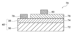
- the composite material piece 40' consists of the substrate 36 and the semiconductor film 38, and the substrate 36 is used as the base substrate 72 and the semiconductor film 38 is used as the n + layer 74 in manufacturing the device. Use.
- a region of 2 mm ⁇ 10 mm from the end on the surface of the composite material piece 40'on the semiconductor film 38 (n + layer 74) side was masked with a sapphire substrate (not shown), and then the n - layer 76 was formed.
- the dopant specifically, tin (II) chloride
- the sapphire substrate (not shown) as masking was removed to expose the n + layer 74.
- a Ti electrode 78 (ohmic electrode, diameter 60 ⁇ m) was formed in the exposed region of the n + layer 74, while a Pt electrode 80 (Schottky electrode, diameter 60 ⁇ m) was formed on the n ⁇ layer. In this way, a horizontal Schottky barrier diode 70 as shown in FIG. 4 was produced.
- the Schottky barrier diode 70 is in the form of a horizontal device in order to easily evaluate the homogeneity of the device, but this example is also used in a vertical device manufactured by removing the base substrate 72. Shows the same tendency as the horizontal device of.
- Examples 2 and 3 A semiconductor film was prepared and various evaluations were carried out in the same manner as in Example 1 except that the apparatus and film forming conditions in the above (1b) and (1c) were changed as shown in Table 1. The results were as shown in Table 1.
- Example 4 Same as Example 1 except that the raw material solution of (1a) was prepared as follows, and the apparatus and film forming conditions in (1b) and (1c) above were changed as shown in Table 1. Then, a semiconductor film was prepared and various evaluations were performed. The results were as shown in Table 1.
- Example 5 The apparatus and film forming conditions in the above (1b) and (1c) were changed as shown in Table 1, and the composite base substrate produced as the substrate 36 in the above (1c) film formation as described below was used. A semiconductor film was prepared and various evaluations were carried out in the same manner as in Example 1 except that it was used. The results were as shown in Table 1.
- the AD film formation conditions were as follows. That is, the carrier gas was N 2, and a ceramic nozzle having a slit having a long side of 5 mm and a short side of 0.3 mm was used.
- the scanning conditions of the nozzle are 1 mm / s scanning speed, 55 mm movement in the direction perpendicular to the long side of the slit and in the forward direction, 5 mm movement in the long side direction of the slit, and vertical and return direction to the long side of the slit.
- the scan is repeated with 55 mm movement, 5 mm movement in the long side direction of the slit and in the direction opposite to the initial position, and when 55 mm is moved from the initial position in the long side direction of the slit, scanning is performed in the opposite direction.
- the cycle of returning to the initial position was set as one cycle, and this was repeated for 300 cycles.
- the set pressure of the transport gas was adjusted to 0.06 MPa, the flow rate was adjusted to 6 L / min, and the pressure in the chamber was adjusted to 100 Pa or less.
- the thickness of the AD film (alignment precursor layer) thus formed was about 60 ⁇ m.
- AD film (alignment precursor layer) separately prepared by the same method as in (a) and (b) above is prepared and passes through the center of the substrate in a direction orthogonal to the plate surface. I cut it like this.
- the cross section of the cut sample was smoothed by lapping with diamond abrasive grains, and mirror-finished by chemical mechanical polishing (CMP) using colloidal silica.
- CMP chemical mechanical polishing
- the orientation precursor layer (hereinafter referred to as the polycrystal part) remaining as polycrystalline and the alignment layer can be identified by the channeling contrast due to the difference in crystal orientation.
- the film thickness of the oriented layer was about 50 ⁇ m, and the film thickness of the polycrystalline portion was about 10 ⁇ m.
- Example 6 The equipment and film formation conditions of (1b) and (1c) above were changed as shown in Table 1, a 10.0 cm (4 inch) composite substrate was prepared and used, and the AD method. A semiconductor film was prepared and various evaluations were carried out in the same manner as in Example 5, except that the film formation range in (1) was expanded to a 110 mm square region. The results were as shown in Table 1.
- Examples 7 and 8 (comparison) Fabrication of semiconductor films and various types in the same manner as in Example 1 except that the apparatus and film forming conditions of the above (1b) and (1c) were changed as shown in Table 1 (for example, the stage rotation speed was set to 0 rpm). Evaluation was performed. The results were as shown in Table 1. Further, FIG. 6 shows a Raman spectrum measured at the outer peripheral point B of the semiconductor film obtained in Example 7.
Landscapes
- Chemical & Material Sciences (AREA)
- Organic Chemistry (AREA)
- Metallurgy (AREA)
- Engineering & Computer Science (AREA)
- Materials Engineering (AREA)
- Chemical Kinetics & Catalysis (AREA)
- Mechanical Engineering (AREA)
- General Chemical & Material Sciences (AREA)
- Physics & Mathematics (AREA)
- Spectroscopy & Molecular Physics (AREA)
- Inorganic Chemistry (AREA)
- Crystallography & Structural Chemistry (AREA)
- General Physics & Mathematics (AREA)
- Dispersion Chemistry (AREA)
- Crystals, And After-Treatments Of Crystals (AREA)
- Chemical Vapour Deposition (AREA)
- Liquid Deposition Of Substances Of Which Semiconductor Devices Are Composed (AREA)
Priority Applications (3)
| Application Number | Priority Date | Filing Date | Title |
|---|---|---|---|
| JP2021545031A JP7410159B2 (ja) | 2019-09-11 | 2019-09-11 | 半導体膜 |
| PCT/JP2019/035694 WO2021048950A1 (ja) | 2019-09-11 | 2019-09-11 | 半導体膜 |
| US17/650,402 US12351906B2 (en) | 2019-09-11 | 2022-02-09 | Semiconductor film |
Applications Claiming Priority (1)
| Application Number | Priority Date | Filing Date | Title |
|---|---|---|---|
| PCT/JP2019/035694 WO2021048950A1 (ja) | 2019-09-11 | 2019-09-11 | 半導体膜 |
Related Child Applications (1)
| Application Number | Title | Priority Date | Filing Date |
|---|---|---|---|
| US17/650,402 Continuation US12351906B2 (en) | 2019-09-11 | 2022-02-09 | Semiconductor film |
Publications (1)
| Publication Number | Publication Date |
|---|---|
| WO2021048950A1 true WO2021048950A1 (ja) | 2021-03-18 |
Family
ID=74866254
Family Applications (1)
| Application Number | Title | Priority Date | Filing Date |
|---|---|---|---|
| PCT/JP2019/035694 Ceased WO2021048950A1 (ja) | 2019-09-11 | 2019-09-11 | 半導体膜 |
Country Status (3)
| Country | Link |
|---|---|
| US (1) | US12351906B2 (https=) |
| JP (1) | JP7410159B2 (https=) |
| WO (1) | WO2021048950A1 (https=) |
Cited By (4)
| Publication number | Priority date | Publication date | Assignee | Title |
|---|---|---|---|---|
| JPWO2023026633A1 (https=) * | 2021-08-27 | 2023-03-02 | ||
| US20240234138A9 (en) * | 2021-03-12 | 2024-07-11 | Shin-Etsu Chemical Co., Ltd. | Oxide semiconductor film and film-forming method the same, semiconductor apparatus |
| WO2024195374A1 (ja) * | 2023-03-23 | 2024-09-26 | 日本碍子株式会社 | 下地基板 |
| WO2026013719A1 (ja) * | 2024-07-08 | 2026-01-15 | 住友電気工業株式会社 | ベータ型三酸化二ガリウム単結晶基板、ベータ型三酸化二ガリウム単結晶の製造方法、およびベータ型三酸化二ガリウム単結晶基板の製造方法 |
Citations (4)
| Publication number | Priority date | Publication date | Assignee | Title |
|---|---|---|---|---|
| JP2015134717A (ja) * | 2015-03-09 | 2015-07-27 | 公立大学法人高知工科大学 | ドーパントを添加した結晶性の高い導電性α型酸化ガリウム薄膜およびその生成方法 |
| JP2015196603A (ja) * | 2014-03-31 | 2015-11-09 | 株式会社Flosfia | 結晶性積層構造体、半導体装置 |
| CN108987257A (zh) * | 2018-07-12 | 2018-12-11 | 南京南大光电工程研究院有限公司 | 利用卤化物气相外延法在Si衬底上生长Ga2O3薄膜的方法 |
| US20190057865A1 (en) * | 2017-08-21 | 2019-02-21 | Flosfia Inc. | Crystalline film, semiconductor device including crystalline film, and method for producing crystalline film |
Family Cites Families (11)
| Publication number | Priority date | Publication date | Assignee | Title |
|---|---|---|---|---|
| JP6067532B2 (ja) | 2013-10-10 | 2017-01-25 | 株式会社Flosfia | 半導体装置 |
| JP6349592B2 (ja) | 2014-07-22 | 2018-07-04 | 株式会社Flosfia | 半導体装置 |
| US10804362B2 (en) * | 2016-08-31 | 2020-10-13 | Flosfia Inc. | Crystalline oxide semiconductor film, crystalline oxide semiconductor device, and crystalline oxide semiconductor system |
| CN109643660B (zh) * | 2016-08-31 | 2024-03-05 | 株式会社Flosfia | p-型氧化物半导体及其制造方法 |
| JP7163540B2 (ja) * | 2017-08-21 | 2022-11-01 | 株式会社Flosfia | 結晶膜の製造方法 |
| JP7166522B2 (ja) * | 2017-08-21 | 2022-11-08 | 株式会社Flosfia | 結晶膜の製造方法 |
| EP3712305A4 (en) * | 2017-11-15 | 2021-11-17 | Flosfia Inc. | P-TYPE OXIDE SEMICONDUCTORIAL LAYER AND METHOD FOR MANUFACTURING THEREOF |
| TW202006945A (zh) * | 2018-07-12 | 2020-02-01 | 日商Flosfia股份有限公司 | 半導體裝置和半導體系統 |
| JP7247945B2 (ja) * | 2020-04-24 | 2023-03-29 | トヨタ自動車株式会社 | 酸化ガリウム系半導体及びその製造方法 |
| CN116018260B (zh) * | 2020-09-24 | 2025-08-05 | 日本碍子株式会社 | 层叠结构体 |
| WO2022230342A1 (ja) * | 2021-04-27 | 2022-11-03 | 日本碍子株式会社 | 複合基板、複合基板の製法及び酸化ガリウム結晶膜の製法 |
-
2019
- 2019-09-11 WO PCT/JP2019/035694 patent/WO2021048950A1/ja not_active Ceased
- 2019-09-11 JP JP2021545031A patent/JP7410159B2/ja active Active
-
2022
- 2022-02-09 US US17/650,402 patent/US12351906B2/en active Active
Patent Citations (4)
| Publication number | Priority date | Publication date | Assignee | Title |
|---|---|---|---|---|
| JP2015196603A (ja) * | 2014-03-31 | 2015-11-09 | 株式会社Flosfia | 結晶性積層構造体、半導体装置 |
| JP2015134717A (ja) * | 2015-03-09 | 2015-07-27 | 公立大学法人高知工科大学 | ドーパントを添加した結晶性の高い導電性α型酸化ガリウム薄膜およびその生成方法 |
| US20190057865A1 (en) * | 2017-08-21 | 2019-02-21 | Flosfia Inc. | Crystalline film, semiconductor device including crystalline film, and method for producing crystalline film |
| CN108987257A (zh) * | 2018-07-12 | 2018-12-11 | 南京南大光电工程研究院有限公司 | 利用卤化物气相外延法在Si衬底上生长Ga2O3薄膜的方法 |
Non-Patent Citations (1)
| Title |
|---|
| D.DOHY ET AL.: "Raman Spectra and Valence Force Field of Single-Crystalline /3 Ga203", JOURNAL OF SOLID STATE CHEMISTRY, vol. 45, no. 2, 15 November 1982 (1982-11-15), pages 180 - 192, XP024193424, DOI: 10.1016/0022-4596(82)90274-2 * |
Cited By (7)
| Publication number | Priority date | Publication date | Assignee | Title |
|---|---|---|---|---|
| US20240234138A9 (en) * | 2021-03-12 | 2024-07-11 | Shin-Etsu Chemical Co., Ltd. | Oxide semiconductor film and film-forming method the same, semiconductor apparatus |
| EP4306676A4 (en) * | 2021-03-12 | 2025-02-19 | Shin-Etsu Chemical Co., Ltd. | SEMICONDUCTOR ARRANGEMENT |
| JPWO2023026633A1 (https=) * | 2021-08-27 | 2023-03-02 | ||
| WO2023026633A1 (ja) * | 2021-08-27 | 2023-03-02 | 日本碍子株式会社 | 半導体膜及び複合基板 |
| JP7620719B2 (ja) | 2021-08-27 | 2025-01-23 | 日本碍子株式会社 | 半導体膜及び複合基板 |
| WO2024195374A1 (ja) * | 2023-03-23 | 2024-09-26 | 日本碍子株式会社 | 下地基板 |
| WO2026013719A1 (ja) * | 2024-07-08 | 2026-01-15 | 住友電気工業株式会社 | ベータ型三酸化二ガリウム単結晶基板、ベータ型三酸化二ガリウム単結晶の製造方法、およびベータ型三酸化二ガリウム単結晶基板の製造方法 |
Also Published As
| Publication number | Publication date |
|---|---|
| JPWO2021048950A1 (https=) | 2021-03-18 |
| US12351906B2 (en) | 2025-07-08 |
| JP7410159B2 (ja) | 2024-01-09 |
| US20220246427A1 (en) | 2022-08-04 |
Similar Documents
| Publication | Publication Date | Title |
|---|---|---|
| US12351906B2 (en) | Semiconductor film | |
| JP7159449B2 (ja) | 下地基板及びその製造方法 | |
| JP7461851B2 (ja) | 半導体膜 | |
| US12159907B2 (en) | Semiconductor film | |
| JP7410009B2 (ja) | 半導体膜 | |
| JP7124207B2 (ja) | 下地基板 | |
| JP7265624B2 (ja) | 半導体膜 | |
| JP7439117B2 (ja) | 下地基板及びその製造方法 | |
| WO2021064816A1 (ja) | 下地基板及びその製造方法 | |
| US20250391657A1 (en) | Base substrate | |
| WO2020261356A1 (ja) | 半導体膜 | |
| JPWO2020195497A1 (ja) | 半導体膜 |
Legal Events
| Date | Code | Title | Description |
|---|---|---|---|
| 121 | Ep: the epo has been informed by wipo that ep was designated in this application |
Ref document number: 19945214 Country of ref document: EP Kind code of ref document: A1 |
|
| ENP | Entry into the national phase |
Ref document number: 2021545031 Country of ref document: JP Kind code of ref document: A |
|
| NENP | Non-entry into the national phase |
Ref country code: DE |
|
| 122 | Ep: pct application non-entry in european phase |
Ref document number: 19945214 Country of ref document: EP Kind code of ref document: A1 |