WO2021006325A1 - フレキシブルプリント配線板、電池配線モジュール及びフレキシブルプリント配線板の製造方法 - Google Patents
フレキシブルプリント配線板、電池配線モジュール及びフレキシブルプリント配線板の製造方法 Download PDFInfo
- Publication number
- WO2021006325A1 WO2021006325A1 PCT/JP2020/026938 JP2020026938W WO2021006325A1 WO 2021006325 A1 WO2021006325 A1 WO 2021006325A1 JP 2020026938 W JP2020026938 W JP 2020026938W WO 2021006325 A1 WO2021006325 A1 WO 2021006325A1
- Authority
- WO
- WIPO (PCT)
- Prior art keywords
- connection terminal
- flexible printed
- wiring board
- printed wiring
- conductive pattern
- Prior art date
- Legal status (The legal status is an assumption and is not a legal conclusion. Google has not performed a legal analysis and makes no representation as to the accuracy of the status listed.)
- Ceased
Links
Images


Classifications
-
- H—ELECTRICITY
- H05—ELECTRIC TECHNIQUES NOT OTHERWISE PROVIDED FOR
- H05K—PRINTED CIRCUITS; CASINGS OR CONSTRUCTIONAL DETAILS OF ELECTRIC APPARATUS; MANUFACTURE OF ASSEMBLAGES OF ELECTRICAL COMPONENTS
- H05K1/00—Printed circuits
- H05K1/02—Details
- H05K1/11—Printed elements for providing electric connections to or between printed circuits
-
- H—ELECTRICITY
- H05—ELECTRIC TECHNIQUES NOT OTHERWISE PROVIDED FOR
- H05K—PRINTED CIRCUITS; CASINGS OR CONSTRUCTIONAL DETAILS OF ELECTRIC APPARATUS; MANUFACTURE OF ASSEMBLAGES OF ELECTRICAL COMPONENTS
- H05K3/00—Apparatus or processes for manufacturing printed circuits
- H05K3/30—Assembling printed circuits with electric components, e.g. with resistors
- H05K3/32—Assembling printed circuits with electric components, e.g. with resistors electrically connecting electric components or wires to printed circuits
- H05K3/34—Assembling printed circuits with electric components, e.g. with resistors electrically connecting electric components or wires to printed circuits by soldering
- H05K3/341—Surface mounted components
-
- H—ELECTRICITY
- H01—ELECTRIC ELEMENTS
- H01M—PROCESSES OR MEANS, e.g. BATTERIES, FOR THE DIRECT CONVERSION OF CHEMICAL ENERGY INTO ELECTRICAL ENERGY
- H01M50/00—Constructional details or processes of manufacture of the non-active parts of electrochemical cells other than fuel cells, e.g. hybrid cells
- H01M50/50—Current conducting connections for cells or batteries
- H01M50/502—Interconnectors for connecting terminals of adjacent batteries; Interconnectors for connecting cells outside a battery casing
- H01M50/519—Interconnectors for connecting terminals of adjacent batteries; Interconnectors for connecting cells outside a battery casing comprising printed circuit boards [PCB]
-
- H—ELECTRICITY
- H05—ELECTRIC TECHNIQUES NOT OTHERWISE PROVIDED FOR
- H05K—PRINTED CIRCUITS; CASINGS OR CONSTRUCTIONAL DETAILS OF ELECTRIC APPARATUS; MANUFACTURE OF ASSEMBLAGES OF ELECTRICAL COMPONENTS
- H05K1/00—Printed circuits
- H05K1/02—Details
- H05K1/0277—Bendability or stretchability details
-
- H—ELECTRICITY
- H05—ELECTRIC TECHNIQUES NOT OTHERWISE PROVIDED FOR
- H05K—PRINTED CIRCUITS; CASINGS OR CONSTRUCTIONAL DETAILS OF ELECTRIC APPARATUS; MANUFACTURE OF ASSEMBLAGES OF ELECTRICAL COMPONENTS
- H05K1/00—Printed circuits
- H05K1/18—Printed circuits structurally associated with non-printed electric components
- H05K1/189—Printed circuits structurally associated with non-printed electric components characterised by the use of flexible or folded printed circuits
-
- H—ELECTRICITY
- H05—ELECTRIC TECHNIQUES NOT OTHERWISE PROVIDED FOR
- H05K—PRINTED CIRCUITS; CASINGS OR CONSTRUCTIONAL DETAILS OF ELECTRIC APPARATUS; MANUFACTURE OF ASSEMBLAGES OF ELECTRICAL COMPONENTS
- H05K3/00—Apparatus or processes for manufacturing printed circuits
- H05K3/40—Forming printed elements for providing electric connections to or between printed circuits
-
- H—ELECTRICITY
- H01—ELECTRIC ELEMENTS
- H01M—PROCESSES OR MEANS, e.g. BATTERIES, FOR THE DIRECT CONVERSION OF CHEMICAL ENERGY INTO ELECTRICAL ENERGY
- H01M2220/00—Batteries for particular applications
- H01M2220/20—Batteries in motive systems, e.g. vehicle, ship, plane
-
- H—ELECTRICITY
- H05—ELECTRIC TECHNIQUES NOT OTHERWISE PROVIDED FOR
- H05K—PRINTED CIRCUITS; CASINGS OR CONSTRUCTIONAL DETAILS OF ELECTRIC APPARATUS; MANUFACTURE OF ASSEMBLAGES OF ELECTRICAL COMPONENTS
- H05K2201/00—Indexing scheme relating to printed circuits covered by H05K1/00
- H05K2201/01—Dielectrics
- H05K2201/0137—Materials
- H05K2201/0154—Polyimide
-
- H—ELECTRICITY
- H05—ELECTRIC TECHNIQUES NOT OTHERWISE PROVIDED FOR
- H05K—PRINTED CIRCUITS; CASINGS OR CONSTRUCTIONAL DETAILS OF ELECTRIC APPARATUS; MANUFACTURE OF ASSEMBLAGES OF ELECTRICAL COMPONENTS
- H05K2201/00—Indexing scheme relating to printed circuits covered by H05K1/00
- H05K2201/03—Conductive materials
- H05K2201/0302—Properties and characteristics in general
- H05K2201/0311—Metallic part with specific elastic properties, e.g. bent piece of metal as electrical contact
-
- H—ELECTRICITY
- H05—ELECTRIC TECHNIQUES NOT OTHERWISE PROVIDED FOR
- H05K—PRINTED CIRCUITS; CASINGS OR CONSTRUCTIONAL DETAILS OF ELECTRIC APPARATUS; MANUFACTURE OF ASSEMBLAGES OF ELECTRICAL COMPONENTS
- H05K2201/00—Indexing scheme relating to printed circuits covered by H05K1/00
- H05K2201/10—Details of components or other objects attached to or integrated in a printed circuit board
- H05K2201/10007—Types of components
- H05K2201/10037—Printed or non-printed battery
-
- H—ELECTRICITY
- H05—ELECTRIC TECHNIQUES NOT OTHERWISE PROVIDED FOR
- H05K—PRINTED CIRCUITS; CASINGS OR CONSTRUCTIONAL DETAILS OF ELECTRIC APPARATUS; MANUFACTURE OF ASSEMBLAGES OF ELECTRICAL COMPONENTS
- H05K2201/00—Indexing scheme relating to printed circuits covered by H05K1/00
- H05K2201/10—Details of components or other objects attached to or integrated in a printed circuit board
- H05K2201/10227—Other objects, e.g. metallic pieces
- H05K2201/1031—Surface mounted metallic connector elements
-
- H—ELECTRICITY
- H05—ELECTRIC TECHNIQUES NOT OTHERWISE PROVIDED FOR
- H05K—PRINTED CIRCUITS; CASINGS OR CONSTRUCTIONAL DETAILS OF ELECTRIC APPARATUS; MANUFACTURE OF ASSEMBLAGES OF ELECTRICAL COMPONENTS
- H05K2201/00—Indexing scheme relating to printed circuits covered by H05K1/00
- H05K2201/10—Details of components or other objects attached to or integrated in a printed circuit board
- H05K2201/10613—Details of electrical connections of non-printed components, e.g. special leads
- H05K2201/10742—Details of leads
- H05K2201/10886—Other details
- H05K2201/10916—Terminals having auxiliary metallic piece, e.g. for soldering
-
- Y—GENERAL TAGGING OF NEW TECHNOLOGICAL DEVELOPMENTS; GENERAL TAGGING OF CROSS-SECTIONAL TECHNOLOGIES SPANNING OVER SEVERAL SECTIONS OF THE IPC; TECHNICAL SUBJECTS COVERED BY FORMER USPC CROSS-REFERENCE ART COLLECTIONS [XRACs] AND DIGESTS
- Y02—TECHNOLOGIES OR APPLICATIONS FOR MITIGATION OR ADAPTATION AGAINST CLIMATE CHANGE
- Y02E—REDUCTION OF GREENHOUSE GAS [GHG] EMISSIONS, RELATED TO ENERGY GENERATION, TRANSMISSION OR DISTRIBUTION
- Y02E60/00—Enabling technologies; Technologies with a potential or indirect contribution to GHG emissions mitigation
- Y02E60/10—Energy storage using batteries
Definitions
- This disclosure relates to a method for manufacturing a flexible printed wiring board, a battery wiring module, and a flexible printed wiring board.
- each electronic component such as a flat coil element constituting the electronic device is mounted on a flexible printed wiring board and has been miniaturized.
- This flexible printed wiring board has a metal connection terminal for connecting to another printed wiring board, an electronic device, or the like on one end edge side (see, for example, Japanese Patent Application Laid-Open No. 2011-159880).
- This connection terminal has a square plate shape and is connected to the conductive pattern of the flexible printed wiring board via a conductive adhesive layer such as solder.
- solder fillet In order to improve the adhesion between the metal connection terminal and the conductive pattern and suppress the occurrence of solder cracks, for example, it is advisable to form a solder fillet at the lower end of the side surface of the connection terminal. In order to stably form this solder fillet, it is necessary to plate the end face of the metal connection terminal.
- the flexible printed wiring board is a flexible printed wiring board including a base film having an insulating property and a conductive pattern laminated on one surface side of the base film, and is the conductive pattern of the above.
- One or more square plate-shaped connection terminals laminated on the conductive pattern via solder at one end are further provided, the connection terminals are made of metal, and both ends thereof are bent to the opposite side to the base film. It has a bent portion and has a plating layer on the outer surface side of the bent portion.
- a method for manufacturing a flexible printed wiring board is a method for manufacturing a flexible printed wiring board including a base film having an insulating property and a conductive pattern laminated on one surface side of the base film.
- a connection in which a connection terminal preparation step for preparing a square plate-shaped connection terminal and a connection terminal prepared in the connection terminal preparation step are laminated on one end edge side of the conductive pattern via solder.
- a terminal laminating step is provided, and as the connection terminal preparation step, a plating layer forming step of forming a plating layer on one surface of a metal plate and the metal plate after the plating layer forming step are formed of a plurality of square metals.
- connection terminal It is provided with a cutting step of cutting into individual pieces and a bending portion forming step of bending both ends of the metal piece after the cutting step so that the plating layer is the outer surface, and in the connection terminal laminating step, the connection terminal is connected.
- the connection terminals are laminated so that the bent portion is on the opposite side of the base film.
- FIG. 1 is a schematic side view of a flexible printed wiring board according to an embodiment of the present disclosure.
- FIG. 2 is a schematic cross-sectional view taken along the line AA of FIG.
- FIG. 3 is a schematic flow chart showing a method of manufacturing a flexible printed wiring board according to an embodiment of the present disclosure.
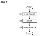
- FIG. 4 is a schematic flow chart showing the connection terminal preparation process of FIG.
- FIG. 5 is a plan view of the battery wiring module 100.
- the metal connection terminal is manufactured by cutting (sheet metal processing) from a metal plate larger than the connection terminal.
- the end face of the connection terminal is exposed to the outside for the first time after this sheet metal processing, and can be plated. Therefore, in the conventional manufacturing of the connection terminal, the end face is plated after the cutting process. Therefore, it is necessary to perform the plating treatment on the metal pieces after cutting, which tends to cause variations in plating quality and increase in processing cost.
- the present disclosure has been made based on the above-mentioned circumstances, and is a flexible printed wiring board capable of improving the adhesion between the connection terminal and the conductive pattern while suppressing variations in plating quality of the connection terminal and processing cost.
- An object of the present invention is to provide a method for manufacturing a flexible printed wiring board. [Effect of this disclosure]
- the flexible printed wiring board of the present disclosure and the method of manufacturing the flexible printed wiring board of the present disclosure can improve the adhesion between the connection terminal and the conductive pattern while suppressing variations in plating quality and processing cost of the connection terminal.
- the flexible printed wiring board according to one aspect of the present disclosure is a flexible printed wiring board including a base film having an insulating property and a conductive pattern laminated on one surface side of the base film, and is the conductive pattern of the above.
- One or more square plate-shaped connection terminals laminated on the conductive pattern via solder at one end are further provided, the connection terminals are made of metal, and both ends thereof are bent to the opposite side to the base film. It has a bent portion and has a plating layer on the outer surface side of the bent portion.
- the flexible printed wiring board has bent portions in which both ends of a square plate-shaped connection terminal are bent to the opposite side of the base film.
- a plating layer on the outer surface side of the bent portion of the flexible printed wiring board, it is easy to form a solder fillet, so that the adhesion between the connection terminal and the conductive pattern can be improved.
- the outer surface of the bent portion is located on the surface of the metal plate before the cutting process, which is the base material of the connection terminal, the outer surface of the bent portion can also be plated before the cutting process of the metal plate. .. Therefore, the flexible printed wiring board can suppress variations in plating quality of connection terminals and processing costs.
- solder fillet is formed between the bent portion and the conductive pattern.
- the bending angle of the bent portion is preferably 1 degree or more and less than 180 degrees. By setting the bending angle within the above range, it is possible to form a solder fillet while suppressing an increase in the area of the connection terminal in a plan view.
- the "bending angle” refers to the angle formed by the central axis of the bent portion and the central axis of the bottom portion.
- the protruding height of the bent portion from the surface of the conductive pattern is preferably 0.05 mm or more and 10 mm or less.
- a method for manufacturing a flexible printed wiring board is a method for manufacturing a flexible printed wiring board including a base film having an insulating property and a conductive pattern laminated on one surface side of the base film.
- a connection in which a connection terminal preparation step for preparing a square plate-shaped connection terminal and a connection terminal prepared in the connection terminal preparation step are laminated on one end edge side of the conductive pattern via solder.
- a terminal laminating step is provided, and as the connection terminal preparation step, a plating layer forming step of forming a plating layer on one surface of a metal plate and the metal plate after the plating layer forming step are formed of a plurality of square metals.
- connection terminal It is provided with a cutting step of cutting into individual pieces and a bending portion forming step of bending both ends of the metal piece after the cutting step so that the plating layer is the outer surface, and in the connection terminal laminating step, the connection terminal is connected.
- the connection terminals are laminated so that the bent portion is on the opposite side of the base film.
- the metal plate is cut into a square shape to obtain a connection terminal. Therefore, by using the method for manufacturing the flexible printed wiring board, it is possible to suppress variations in plating quality of connection terminals and processing costs. Further, in the method of manufacturing the flexible printed wiring board, both ends of the metal plate after cutting are bent to form a connection terminal. Therefore, when the connection terminal is laminated on one end edge side of the conductive pattern via solder, a solder fillet is formed. It is easy to form, and the adhesion between the connection terminal and the conductive pattern can be improved. [Details of Embodiments of the present disclosure] Hereinafter, embodiments of the flexible printed wiring board and the method for manufacturing the flexible printed wiring board according to the present disclosure will be described in detail with reference to the drawings.
- the flexible printed wiring board has an insulating base film 1, a conductive pattern 2 laminated on one surface side of the base film 1, and one end edge side of the conductive pattern 2. It mainly includes a plurality of square plate-shaped connection terminals 4 laminated on the conductive pattern 2 via the solder 3, and a coverlay 5 laminated on one surface of the base film 1 or the conductive pattern 2.
- the base film 1 is a member that supports the conductive pattern 2 and is a structural material that guarantees the strength of the flexible printed wiring board. Further, the base film 1 has insulating properties and flexibility.
- the main components of the base film 1 include, for example, polyimide, liquid crystal polymers typified by liquid crystal polyester, polyethylene terephthalate, polyethylene naphthalate, polyphenylene ether, soft materials such as fluororesin, paper phenol, paper epoxy, glass composite, and glass epoxy.
- a rigid material such as a glass base material, a rigid flexible material obtained by combining a soft material and a hard material, and the like can be used.
- polyimide having excellent heat resistance is preferable.
- the base film 1 may be made porous, or may contain a filler, an additive, or the like.
- the "main component” means a component having the highest content, for example, a component having a content of 50% by mass or more.
- the thickness of the base film 1 is not particularly limited, but the lower limit of the average thickness of the base film 1 is preferably 5 ⁇ m, more preferably 12 ⁇ m.
- the upper limit of the average thickness of the base film 1 is preferably 500 ⁇ m, more preferably 200 ⁇ m. If the average thickness of the base film 1 is less than the above lower limit, the strength of the base film 1 may be insufficient. On the other hand, if the average thickness of the base film 1 exceeds the above upper limit, the flexibility of the flexible printed wiring board may be insufficient.
- the conductive pattern 2 constitutes a structure such as an electric wiring structure, a ground, and a shield.
- the material forming the conductive pattern 2 is not particularly limited as long as it is a conductive material, and examples thereof include metals such as copper, aluminum, and nickel. Generally, copper, which is relatively inexpensive and has a high conductivity, is used. Used. Further, the surface of the conductive pattern 2 may be plated.
- the lower limit of the average thickness of the conductive pattern 2 is preferably 2 ⁇ m, more preferably 5 ⁇ m.
- the upper limit of the average thickness of the conductive pattern 2 is preferably 100 ⁇ m, more preferably 70 ⁇ m. If the average thickness of the conductive pattern 2 is less than the above lower limit, the conductivity of the conductive pattern 2 may be insufficient. On the contrary, if the average thickness of the conductive pattern 2 exceeds the above upper limit, the flexible printed wiring board may become unnecessarily thick.
- the flexible printed wiring board is provided with a terminal connection region 2a on one end edge side of the conductive pattern 2.
- the terminal connection area 2a is an area for connecting the flexible printed wiring board to another electronic device or the like via a connection terminal 4 described later.
- the coverlay 5 described later is removed.
- the shape of the terminal connection region 2a is not particularly limited as long as it can be electrically connected to each connection terminal 4, but can be, for example, a square shape.
- the size of the terminal connection region 2a is appropriately determined depending on the size of the connection terminal 4, and can be, for example, an average width of 0.5 mm or more and 3 mm or less, and an average length of 3 mm or more and 50 mm or less.
- the connection terminal 4 is a component for connecting the flexible printed wiring board to other electronic devices and the like. As described above, the connection terminal 4 is laminated on the terminal connection region 2a on the edge side of one end of the conductive pattern 2 via the solder 3. Further, the connection terminal 4 has a bent portion 4a whose both ends are bent toward the opposite side of the base film 1. By the bent portion 4a, the connection terminal 4 is configured to have a U-shaped cross section.
- connection terminal 4 is made of metal.
- the metal include annealed copper, brass, phosphor bronze, and aluminum.
- the connection terminal 4 has a plating layer 4b on the entire outer surface side including the outer surface of the bent portion 4a. Further, the connection terminal 4 does not have a plating layer on the end face.
- Examples of the plating of the plating layer 4b on the outer surface side of the bent portion 4a include Sn plating, Ni plating, and Au plating. Of these, Ni plating, which is inexpensive, has excellent corrosion resistance, and easily forms the solder fillet 3a described later, is preferable.
- the thickness of the plating layer 4b is not particularly limited, but can be, for example, 0.01 ⁇ m or more and 100 ⁇ m or less.
- the lower limit of the average thickness of the connection terminal 4 (the average thickness of the entire connection including the plating layer) is preferably 0.05 mm, more preferably 0.1 mm.
- the upper limit of the average thickness of the connection terminal 4 is preferably 5.0 mm, more preferably 1.0 mm. If the average thickness of the connection terminals 4 is less than the above lower limit, the strength of the connection terminals 4 may be insufficient. On the contrary, when the average thickness of the connection terminal 4 exceeds the above upper limit, the connection terminal 4 becomes unnecessarily thick, it becomes difficult to bend both ends of the connection terminal 4, or the weight of the connection terminal 4 makes the flexible print. It may be difficult to handle the wiring board.
- the average length of the connection terminal 4 and the average width of the bottom are appropriately determined according to the terminal shape of the electronic device to be connected and the like.
- the average length is 3 mm or more and 50 mm or less
- the average width is 0.5 mm or more and 3 mm or less. it can.
- the “bottom” of the connection terminal 4 refers to a portion (W in FIG. 2) of the portion bonded to the conductive pattern 2 by the solder 3 excluding the curved portion of the U-shaped connection terminal 4.
- the lower limit of the protruding height (H in FIG. 2) of the bent portion 4a from the surface of the conductive pattern 2 is preferably 0.05 mm, more preferably 0.5 mm, and particularly preferably 1 mm.
- the upper limit of the protrusion height 10 mm is preferable, 3 mm is more preferable, and 2 mm is particularly preferable. If the protruding height is less than the lower limit, it may be difficult to bend both ends of the connection terminal 4. On the contrary, if the protruding height exceeds the upper limit, the connection terminal 4 becomes unnecessarily high, which may make it difficult to handle the flexible printed wiring board.
- the bending angle ( ⁇ in FIG. 2) of the bent portion 4a As the lower limit of the bending angle ( ⁇ in FIG. 2) of the bent portion 4a, 1 degree is preferable, 45 degrees is more preferable, and 60 degrees is particularly preferable.
- the bending angle is preferably less than 180 degrees, more preferably less than 90 degrees, and particularly preferably less than 80 degrees. If the bending angle is less than the above lower limit, the connection terminal 4 unnecessarily expands in the width direction, which may make it difficult to handle the flexible printed wiring board. On the contrary, if the bending angle is at least the above upper limit, it may be difficult to form the solder fillet 3a.
- the lower limit of the ratio of the radius of curvature of the curved portion of the U-shaped connection terminal 4 to the average thickness of the connection terminal 4 is preferably 1.5 times, more preferably 1.8 times.
- the upper limit of the ratio of the radius of curvature is preferably 3 times, more preferably 2.5 times. If the ratio of the radius of curvature is less than the above lower limit, the connection terminal 4 may be easily damaged at the curved portion. On the contrary, when the ratio of the radius of curvature exceeds the above upper limit, the connection terminal 4 unnecessarily expands in the width direction, which may make it difficult to handle the flexible printed wiring board.
- the lower limit of the radius of curvature of the curved portion of the U-shaped connection terminal 4 0.1 mm is preferable, and 0.2 mm is more preferable.
- the upper limit of the radius of curvature is preferably 1 mm, more preferably 0.5 mm. If the radius of curvature is less than the lower limit, the connection terminal 4 may be easily damaged at the curved portion. On the contrary, if the radius of curvature exceeds the upper limit, the connection terminal 4 unnecessarily expands in the width direction, which may make it difficult to handle the flexible printed wiring board.
- connection terminal 4 is laminated on the terminal connection region 2a of the conductive pattern 2 via the solder 3.
- the type of the solder 3 is not particularly limited, but for example, a known lead-free solder or the like can be used.
- the solder 3 is mainly laminated between the bottom of the connection terminal 4 and the conductive pattern 2.
- the lower limit of the average thickness of the solder 3 (the average distance between the bottom of the connection terminal 4 and the conductive pattern 2) of the laminated portion is preferably 10 ⁇ m, more preferably 100 ⁇ m.
- the upper limit of the average thickness of the solder 3 is preferably 300 ⁇ m, more preferably 200 ⁇ m. If the average thickness of the solder 3 is less than the above lower limit, the adhesive strength between the connection terminal 4 and the conductive pattern 2 may be insufficient. On the contrary, when the average thickness of the solder 3 exceeds the upper limit, the amount of the solder 3 is unnecessarily increased, which may reduce the manufacturing efficiency or the manufacturing cost.
- solder 3 is laminated between the lower end (curved portion) of the bent portion 4a and the conductive pattern 2 to form the solder fillet 3a.
- the solder fillet 3a between the bent portion 4a and the conductive pattern 2 in this way, the contact area between the connection terminal 4 and the conductive pattern 2 can be increased, the adhesion can be improved, and cracks in the solder 3 occur. Etc. can be suppressed.
- the height of the formed solder fillet 3a is determined by the viscosity of the solder 3 used, the radius of curvature of the curved portion at the lower end of the bent portion 4a, and the like, but is the same height as the top surface of the bottom of the connection terminal 4 or the connection terminal 4.
- the height is preferably larger than the top surface of the bottom.
- the coverlay 5 protects the conductive pattern 2 from external force, moisture, and the like.
- the coverlay 5 has a cover film and an adhesive layer.
- the coverlay 5 is formed by laminating a cover film on the surface of the conductive pattern 2 opposite to the base film 1 via the adhesive layer.
- the material of the cover film is not particularly limited, but for example, the same material as the resin constituting the base film 1 can be used.
- the upper limit of the average thickness of the cover film is preferably 50 ⁇ m, more preferably 30 ⁇ m. If the average thickness of the cover film is less than the above lower limit, the insulating property may be insufficient. On the contrary, if the average thickness of the cover film exceeds the above upper limit, the flexibility of the flexible printed wiring board may be impaired. (Adhesive layer) The adhesive layer fixes the cover film to the conductive pattern 2 and the base film 1.
- the material of the adhesive layer is not particularly limited as long as the cover film can be fixed to the conductive pattern 2 and the base film 1, but those having excellent flexibility and heat resistance are preferable, and for example, polyimide, polyamide, epoxy, etc. Butyral, acrylic and the like can be mentioned. Further, a thermosetting resin is preferable in terms of heat resistance.
- the average thickness of the adhesive layer of the coverlay 5 is not particularly limited, but the lower limit of the average thickness of the adhesive layer is preferably, for example, 5 ⁇ m, and more preferably 10 ⁇ m.
- the upper limit of the average thickness of the adhesive layer for example, 100 ⁇ m is preferable, and 80 ⁇ m is more preferable. If the average thickness of the adhesive layer is less than the above lower limit, the adhesiveness may be insufficient. On the contrary, if the average thickness of the adhesive layer exceeds the above upper limit, the flexibility of the flexible printed wiring board may be impaired.
- the method for manufacturing the flexible printed wiring board mainly includes a flexible printed wiring board forming step S1, a connection terminal preparation step S2, and a connection terminal stacking step S3.
- a flexible printed wiring board forming step S1 the base film 1 having an insulating property, the conductive pattern 2 laminated on one surface side of the base film 1, and the conductive pattern 2 laminated on one surface of the base film 1 or the conductive pattern 2 are laminated.
- a flexible printed wiring board main body including the coverlay 5 to be formed is formed. Specifically, the procedure is as follows.
- a conductor layer is formed on one surface of the base film 1.
- the conductor layer can be formed, for example, by adhering a foil-shaped conductor with an adhesive or by a known film forming method.
- Examples of the conductor include copper, silver, gold, nickel and the like.
- the adhesive is not particularly limited as long as it can adhere the conductor to the base film 1, and various known adhesives can be used.
- Examples of the film forming method include thin film deposition and plating.
- the conductor layer is preferably formed by adhering a copper foil to the base film 1 using a polyimide adhesive.
- the conductor layer is patterned to form the conductive pattern 2.
- the patterning of the conductor layer can be performed by a known method, for example, photoetching. Photoetching is performed by forming a resist film having a predetermined pattern on one surface of the conductor layer, and then treating the conductor layer exposed from the resist film with an etching solution to remove the resist film.
- the coverlay 5 is laminated so as to cover the conductive pattern 2 except for the terminal connection region 2a on the edge side of one end of the conductive pattern 2.
- an adhesive layer is laminated on the surface of the base film 1 on which the conductive pattern 2 is formed, and a cover film is laminated on the adhesive layer.
- the adhesive layer may be laminated on the cover film in advance, and the surface on the side where the adhesive layer of the cover film is laminated may be made to face the conductive pattern 2 for adhesion.
- Adhesion of the cover film using an adhesive can usually be performed by thermocompression bonding.
- the temperature and pressure at the time of thermocompression bonding may be appropriately determined according to the type and composition of the adhesive to be used.
- the flexible printed wiring board forming step S1 may be performed after the connection terminal preparation step S2 described later. That is, the order of the flexible printed wiring board forming step S1 and the connection terminal preparation step S2 does not matter.
- the connection terminal preparation step S2 the square plate-shaped connection terminal 4 is prepared.
- the method for manufacturing the flexible printed wiring board includes a plating layer forming step S21, a cutting step S22, and a bent portion forming step S23 as a connection terminal preparation step S2. (Plating layer forming process)
- a plating layer is formed on one surface of the metal plate.
- the metal plate used in the plating layer forming step S21 is a metal plate of the same type as the metal forming the connection terminal 4. Further, the metal plate has a size that allows a plurality of connection terminals 4 to be cut out in the cutting step S22 described later.
- the method for forming the plating layer is not particularly limited, and for example, a known electroplating method or electroless plating method can be used.
- the metal plate after the plating layer forming step S21 is cut into a plurality of square metal pieces.
- the shape and size of the metal piece to be cut is equal to the shape and size of the bent portions 4a at both ends of the desired connection terminal 4 spread out on the same plane as the bottom. That is, the shape and size of the metal piece to be cut is the shape and size that the connection terminal 4 can be formed by simply bending the metal piece.
- the method for cutting the metal plate is not particularly limited, and for example, a known metal cutting machine can be used.
- a known metal cutting machine can be used.
- bent portion forming process In the bent portion forming step S23, both ends of the metal piece after the cutting step S22 are bent into a U-shaped cross section so that the plating layer is the outer surface.
- the method of bending the above-mentioned metal piece is not particularly limited, and for example, mold processing can be used.
- connection terminal 4 having a bent portion 4a whose both ends are bent and having a plating layer 4b on the outer surface side of the bent portion 4a.
- the number of connection terminals 4 to be prepared is at least one of the connection terminals laminated on the flexible printed wiring board main body. If there is a surplus in the number of connection terminals 4, the surplus connection terminals 4 may be laminated on another flexible printed wiring board main body.
- connection terminal stacking step S3 the connection terminals 4 prepared in the connection terminal preparation step S2 are laminated on the conductive pattern 2 via the solder 3 on one end edge side of the conductive pattern 2.
- connection terminals 4 are laminated so that the bent portion 4a of the connection terminal 4 is on the opposite side to the base film 1.
- connection terminals 4 can be laminated via the solder 3 by the following procedure, for example.
- the solder 3 is provided in the terminal connection region 2a of the conductive pattern 2.
- the connection terminal 4 is placed on the solder 3 so that the bent portion 4a is on the opposite side of the base film 1, that is, the U-shaped bottom portion is in contact with the solder 3.
- the connection terminal 4 can be soldered to the conductive pattern 2.
- solder 3 becomes the lower end (bent portion) of the bent portion 4a and the conductive pattern 2.
- the solder fillet 3a can be formed by being laminated between the two.
- connection terminals 4 are laminated on the respective terminal connection areas 2a.
- the connection terminals 4 may be laminated one by one by repeating the connection terminal lamination step S3, but from the viewpoint of manufacturing efficiency, a plurality of connection terminals 4 are placed at one time and soldered by one reflow. It is preferable to do so.
- connection terminal 4 In the method for manufacturing a flexible printed wiring board, after forming a plating layer on a metal plate, the metal plate is cut into a square shape to obtain a connection terminal 4. Therefore, by using the method for manufacturing the flexible printed wiring board, it is possible to suppress variations in plating quality and processing costs of the connection terminal 4. Further, in the method for manufacturing the flexible printed wiring board, both ends of the metal plate after cutting are bent to form the connection terminal 4, so that when the connection terminal 4 is laminated on one end edge side of the conductive pattern 2 via the solder 3. The solder fillet 3a can be easily formed, and the adhesion between the connection terminal 4 and the conductive pattern 2 can be improved.
- the flexible printed wiring board has a bent portion 4a in which both ends of the square plate-shaped connection terminal 4 are bent to the opposite side to the base film 1. Therefore, since the outer surface of the bent portion 4a can also be plated before the metal plate that is the base material of the connecting terminal 4 is cut, variations in the plating quality of the connecting terminal 4 and processing costs can be suppressed. The adhesion between the terminal 4 and the conductive pattern 2 can be improved.
- connection terminals may be one.
- the plating layer is provided on the entire outer surface side of the bent portion of the connection terminal, but the plating layer is arranged only on a part of the outer surface side of the bent portion of the connection terminal, for example, at a position where it comes into contact with solder. It may be installed.
- the flexible printed wiring board provided with the coverlay has been described, but the coverlay is not an essential component and can be omitted.
- the coverlay is not an essential component and can be omitted.
- one surface of the base film or the conductive pattern may be covered with an insulating layer having another configuration.
- FIG. 5 is a plan view of the battery wiring module 100.
- the battery wiring module 100 includes a flexible printed wiring board 10, an insulating protector 110, a bus bar 120, a relay member 130, and a connector 140.
- the flexible printed wiring board 10 is the above-mentioned flexible printed wiring board.
- the insulation protector 110 is a plate-shaped member.
- the insulating protector 110 is made of an insulating material. This insulating material is, for example, an insulating synthetic resin.
- a flexible printed wiring board 10 is placed on the upper surface of the insulation protector 110.
- the bus bar 120 is a plate-shaped member formed of a conductive material.
- This conductive material is, for example, a metallic material.
- the metal material is, for example, copper, copper alloy, aluminum, aluminum alloy, stainless steel (SUS) and the like.
- the bus bar 120 is electrically connected to a power storage element (not shown).
- This power storage element is, for example, a secondary battery. An arbitrary number of power storage elements are connected in series or in parallel by the bus bar 120.
- the relay member 130 is a plate-shaped member formed of a conductive material.
- This conductive material is, for example, a metallic material.
- the metal material is, for example, copper, copper alloy, aluminum, aluminum alloy, stainless steel (SUS), nickel, nickel alloy and the like.
- the relay member 130 electrically connects the extra length absorbing portion of the flexible printed wiring board 10 and the bus bar 120.
- the battery wiring module 100 does not have to have the relay member 130.
- the bus bar 120 is electrically connected to the extra length absorbing portion of the flexible printed wiring board 10 without going through the relay member 130.
- the battery wiring module 100 is electrically connected to an external device or the like by the connector 140.
- the flexible printed wiring board of the present disclosure is applicable to the battery wiring module 100 attached to the power storage module including the power storage element.
- the flexible printed wiring board of the present disclosure and the method of manufacturing the flexible printed wiring board of the present disclosure ensure adhesion between the connection terminal and the conductive pattern while suppressing variations in plating quality and processing costs of the connection terminal. Can be improved.
Landscapes
- Engineering & Computer Science (AREA)
- Microelectronics & Electronic Packaging (AREA)
- Manufacturing & Machinery (AREA)
- Chemical & Material Sciences (AREA)
- Chemical Kinetics & Catalysis (AREA)
- Electrochemistry (AREA)
- General Chemical & Material Sciences (AREA)
- Structure Of Printed Boards (AREA)
Priority Applications (3)
| Application Number | Priority Date | Filing Date | Title |
|---|---|---|---|
| CN202080048048.3A CN114097309A (zh) | 2019-07-10 | 2020-07-09 | 柔性印刷配线板、电池配线模块及柔性印刷配线板的制造方法 |
| JP2021530733A JPWO2021006325A1 (https=) | 2019-07-10 | 2020-07-09 | |
| US17/624,630 US20220272839A1 (en) | 2019-07-10 | 2020-07-09 | Flexible printed wiring board, battery wiring module, and method of manufacturing flexible printed wiring board |
Applications Claiming Priority (2)
| Application Number | Priority Date | Filing Date | Title |
|---|---|---|---|
| JP2019-128681 | 2019-07-10 | ||
| JP2019128681 | 2019-07-10 |
Publications (1)
| Publication Number | Publication Date |
|---|---|
| WO2021006325A1 true WO2021006325A1 (ja) | 2021-01-14 |
Family
ID=74113773
Family Applications (1)
| Application Number | Title | Priority Date | Filing Date |
|---|---|---|---|
| PCT/JP2020/026938 Ceased WO2021006325A1 (ja) | 2019-07-10 | 2020-07-09 | フレキシブルプリント配線板、電池配線モジュール及びフレキシブルプリント配線板の製造方法 |
Country Status (4)
| Country | Link |
|---|---|
| US (1) | US20220272839A1 (https=) |
| JP (1) | JPWO2021006325A1 (https=) |
| CN (1) | CN114097309A (https=) |
| WO (1) | WO2021006325A1 (https=) |
Cited By (1)
| Publication number | Priority date | Publication date | Assignee | Title |
|---|---|---|---|---|
| WO2024171603A1 (ja) * | 2023-02-16 | 2024-08-22 | 株式会社デンソー | バスバーモジュール、および、電池パック |
Citations (5)
| Publication number | Priority date | Publication date | Assignee | Title |
|---|---|---|---|---|
| US4900279A (en) * | 1989-04-24 | 1990-02-13 | Die Tech, Inc. | Solder terminal |
| JP2004127715A (ja) * | 2002-10-02 | 2004-04-22 | Rohm Co Ltd | フラットフレキシブルケーブルの耐熱性回路基板に対する半田接続構造及び接続方法 |
| JP2008166021A (ja) * | 2006-12-27 | 2008-07-17 | Nec Saitama Ltd | 電池の接続端子構造 |
| JP2014229506A (ja) * | 2013-05-23 | 2014-12-08 | オムロンオートモーティブエレクトロニクス株式会社 | 端子、電子制御装置 |
| JP2018018612A (ja) * | 2016-07-26 | 2018-02-01 | 株式会社オートネットワーク技術研究所 | 電池用配線モジュール |
Family Cites Families (11)
| Publication number | Priority date | Publication date | Assignee | Title |
|---|---|---|---|---|
| US5411420A (en) * | 1993-05-27 | 1995-05-02 | Die Tech, Inc. | Solder terminal strip |
| JPH09232499A (ja) * | 1996-02-26 | 1997-09-05 | Canon Inc | 半導体装置 |
| JP3734138B2 (ja) * | 2000-02-18 | 2006-01-11 | 矢崎総業株式会社 | フラットケーブル用ターミナル |
| TWM357746U (en) * | 2008-12-09 | 2009-05-21 | Htc Corp | Electronic device and connector assembly |
| KR101786512B1 (ko) * | 2010-07-26 | 2017-10-18 | 엘지전자 주식회사 | 다층 연성회로기판의 제조방법 |
| EP2799595A1 (de) * | 2013-05-03 | 2014-11-05 | Delphi Technologies, Inc. | Elektrisches Kontaktelement |
| CN105379022B (zh) * | 2013-07-11 | 2017-09-12 | 日本压着端子制造株式会社 | 端子及采用端子的连接结构 |
| JP6356974B2 (ja) * | 2014-02-03 | 2018-07-11 | モレックス エルエルシー | 金属端子 |
| JP6556175B2 (ja) * | 2017-02-28 | 2019-08-07 | 矢崎総業株式会社 | 導電モジュール、及び、電池パック |
| JP2019021443A (ja) * | 2017-07-13 | 2019-02-07 | 株式会社オートネットワーク技術研究所 | 端子及び端子付き基板 |
| JP2019036616A (ja) * | 2017-08-14 | 2019-03-07 | 住友電気工業株式会社 | フレキシブルプリント配線板 |
-
2020
- 2020-07-09 JP JP2021530733A patent/JPWO2021006325A1/ja active Pending
- 2020-07-09 WO PCT/JP2020/026938 patent/WO2021006325A1/ja not_active Ceased
- 2020-07-09 CN CN202080048048.3A patent/CN114097309A/zh active Pending
- 2020-07-09 US US17/624,630 patent/US20220272839A1/en not_active Abandoned
Patent Citations (5)
| Publication number | Priority date | Publication date | Assignee | Title |
|---|---|---|---|---|
| US4900279A (en) * | 1989-04-24 | 1990-02-13 | Die Tech, Inc. | Solder terminal |
| JP2004127715A (ja) * | 2002-10-02 | 2004-04-22 | Rohm Co Ltd | フラットフレキシブルケーブルの耐熱性回路基板に対する半田接続構造及び接続方法 |
| JP2008166021A (ja) * | 2006-12-27 | 2008-07-17 | Nec Saitama Ltd | 電池の接続端子構造 |
| JP2014229506A (ja) * | 2013-05-23 | 2014-12-08 | オムロンオートモーティブエレクトロニクス株式会社 | 端子、電子制御装置 |
| JP2018018612A (ja) * | 2016-07-26 | 2018-02-01 | 株式会社オートネットワーク技術研究所 | 電池用配線モジュール |
Cited By (2)
| Publication number | Priority date | Publication date | Assignee | Title |
|---|---|---|---|---|
| WO2024171603A1 (ja) * | 2023-02-16 | 2024-08-22 | 株式会社デンソー | バスバーモジュール、および、電池パック |
| JP2024116720A (ja) * | 2023-02-16 | 2024-08-28 | 株式会社デンソー | バスバーモジュール、および、電池パック |
Also Published As
| Publication number | Publication date |
|---|---|
| JPWO2021006325A1 (https=) | 2021-01-14 |
| CN114097309A (zh) | 2022-02-25 |
| US20220272839A1 (en) | 2022-08-25 |
Similar Documents
| Publication | Publication Date | Title |
|---|---|---|
| JP6959066B2 (ja) | フレキシブルプリント配線板 | |
| EP2099269B1 (en) | Solderable elastic electric contact terminal | |
| US11051399B2 (en) | Flexible printed circuit board | |
| US11483928B2 (en) | Flexible printed circuit board | |
| JP6959226B2 (ja) | フレキシブルプリント配線板、接続体の製造方法及び接続体 | |
| CN101897243A (zh) | 电路板、电路板的制造方法及覆盖膜 | |
| US20210185807A1 (en) | Resin multilayer board | |
| WO2021006325A1 (ja) | フレキシブルプリント配線板、電池配線モジュール及びフレキシブルプリント配線板の製造方法 | |
| JP2014096260A (ja) | フラット配線材及びそれを用いた実装体 | |
| JP7478732B2 (ja) | フレキシブルプリント配線板及び電池配線モジュール | |
| JP6959342B2 (ja) | フレキシブルプリント配線板の製造方法 | |
| CN114079183B (zh) | 板对板连接结构及其制备方法 | |
| JP2019096659A (ja) | 電子部品および電子部品の製造方法 | |
| JP2006033559A (ja) | 部品実装用ラミネート導体及びアンテナ部品 | |
| WO2024219282A1 (ja) | 回路基板及び回路基板の製造方法 | |
| JP6406453B2 (ja) | 樹脂基板、樹脂基板の製造方法 | |
| KR20150024242A (ko) | 솔더링이 가능한 인테나 및 그 제조방법 | |
| WO2021006324A1 (ja) | フレキシブルプリント配線板及び電池配線モジュール | |
| JP2012119497A (ja) | フレキシブルプリント配線板、電子回路モジュール、電子機器 | |
| JP2009147224A (ja) | フレキシブルプリント配線板の製造方法 |
Legal Events
| Date | Code | Title | Description |
|---|---|---|---|
| 121 | Ep: the epo has been informed by wipo that ep was designated in this application |
Ref document number: 20836856 Country of ref document: EP Kind code of ref document: A1 |
|
| ENP | Entry into the national phase |
Ref document number: 2021530733 Country of ref document: JP Kind code of ref document: A |
|
| 122 | Ep: pct application non-entry in european phase |
Ref document number: 20836856 Country of ref document: EP Kind code of ref document: A1 |