WO2020255695A1 - コネクタ装置 - Google Patents
コネクタ装置 Download PDFInfo
- Publication number
- WO2020255695A1 WO2020255695A1 PCT/JP2020/021679 JP2020021679W WO2020255695A1 WO 2020255695 A1 WO2020255695 A1 WO 2020255695A1 JP 2020021679 W JP2020021679 W JP 2020021679W WO 2020255695 A1 WO2020255695 A1 WO 2020255695A1
- Authority
- WO
- WIPO (PCT)
- Prior art keywords
- opening
- case
- holding member
- terminal holding
- terminal
- Prior art date
- Legal status (The legal status is an assumption and is not a legal conclusion. Google has not performed a legal analysis and makes no representation as to the accuracy of the status listed.)
- Ceased
Links
Images



Classifications
-
- H—ELECTRICITY
- H01—ELECTRIC ELEMENTS
- H01R—ELECTRICALLY-CONDUCTIVE CONNECTIONS; STRUCTURAL ASSOCIATIONS OF A PLURALITY OF MUTUALLY-INSULATED ELECTRICAL CONNECTING ELEMENTS; COUPLING DEVICES; CURRENT COLLECTORS
- H01R13/00—Details of coupling devices of the kinds covered by groups H01R12/70 or H01R24/00 - H01R33/00
- H01R13/46—Bases; Cases
- H01R13/52—Dustproof, splashproof, drip-proof, waterproof, or flameproof cases
- H01R13/5202—Sealing means between parts of housing or between housing part and a wall, e.g. sealing rings
-
- H—ELECTRICITY
- H01—ELECTRIC ELEMENTS
- H01R—ELECTRICALLY-CONDUCTIVE CONNECTIONS; STRUCTURAL ASSOCIATIONS OF A PLURALITY OF MUTUALLY-INSULATED ELECTRICAL CONNECTING ELEMENTS; COUPLING DEVICES; CURRENT COLLECTORS
- H01R12/00—Structural associations of a plurality of mutually-insulated electrical connecting elements, specially adapted for printed circuits, e.g. printed circuit boards [PCB], flat or ribbon cables, or like generally planar structures, e.g. terminal strips, terminal blocks; Coupling devices specially adapted for printed circuits, flat or ribbon cables, or like generally planar structures; Terminals specially adapted for contact with, or insertion into, printed circuits, flat or ribbon cables, or like generally planar structures
- H01R12/50—Fixed connections
- H01R12/51—Fixed connections for rigid printed circuits or like structures
- H01R12/515—Terminal blocks providing connections to wires or cables
-
- H—ELECTRICITY
- H01—ELECTRIC ELEMENTS
- H01R—ELECTRICALLY-CONDUCTIVE CONNECTIONS; STRUCTURAL ASSOCIATIONS OF A PLURALITY OF MUTUALLY-INSULATED ELECTRICAL CONNECTING ELEMENTS; COUPLING DEVICES; CURRENT COLLECTORS
- H01R12/00—Structural associations of a plurality of mutually-insulated electrical connecting elements, specially adapted for printed circuits, e.g. printed circuit boards [PCB], flat or ribbon cables, or like generally planar structures, e.g. terminal strips, terminal blocks; Coupling devices specially adapted for printed circuits, flat or ribbon cables, or like generally planar structures; Terminals specially adapted for contact with, or insertion into, printed circuits, flat or ribbon cables, or like generally planar structures
- H01R12/70—Coupling devices
- H01R12/71—Coupling devices for rigid printing circuits or like structures
- H01R12/72—Coupling devices for rigid printing circuits or like structures coupling with the edge of the rigid printed circuits or like structures
- H01R12/722—Coupling devices for rigid printing circuits or like structures coupling with the edge of the rigid printed circuits or like structures coupling devices mounted on the edge of the printed circuits
- H01R12/724—Coupling devices for rigid printing circuits or like structures coupling with the edge of the rigid printed circuits or like structures coupling devices mounted on the edge of the printed circuits containing contact members forming a right angle
-
- H—ELECTRICITY
- H01—ELECTRIC ELEMENTS
- H01R—ELECTRICALLY-CONDUCTIVE CONNECTIONS; STRUCTURAL ASSOCIATIONS OF A PLURALITY OF MUTUALLY-INSULATED ELECTRICAL CONNECTING ELEMENTS; COUPLING DEVICES; CURRENT COLLECTORS
- H01R13/00—Details of coupling devices of the kinds covered by groups H01R12/70 or H01R24/00 - H01R33/00
- H01R13/02—Contact members
-
- H—ELECTRICITY
- H01—ELECTRIC ELEMENTS
- H01R—ELECTRICALLY-CONDUCTIVE CONNECTIONS; STRUCTURAL ASSOCIATIONS OF A PLURALITY OF MUTUALLY-INSULATED ELECTRICAL CONNECTING ELEMENTS; COUPLING DEVICES; CURRENT COLLECTORS
- H01R13/00—Details of coupling devices of the kinds covered by groups H01R12/70 or H01R24/00 - H01R33/00
- H01R13/40—Securing contact members in or to a base or case; Insulating of contact members
-
- H—ELECTRICITY
- H01—ELECTRIC ELEMENTS
- H01R—ELECTRICALLY-CONDUCTIVE CONNECTIONS; STRUCTURAL ASSOCIATIONS OF A PLURALITY OF MUTUALLY-INSULATED ELECTRICAL CONNECTING ELEMENTS; COUPLING DEVICES; CURRENT COLLECTORS
- H01R13/00—Details of coupling devices of the kinds covered by groups H01R12/70 or H01R24/00 - H01R33/00
- H01R13/46—Bases; Cases
- H01R13/502—Bases; Cases composed of different pieces
Definitions
- This disclosure relates to a connector device.
- Patent Document 1 discloses a connector device having a case having a square opening on the front surface and a connector for a substrate attached to the opening.
- the board connector has a housing and an L-shaped terminal fitting attached to the housing so as to penetrate in the front-rear direction.
- the terminal fitting has a board connection portion that extends downward in the case.
- the lower end of the board connection is located below the opening and is connected to the circuit board.
- the case is composed of a case upper lid having an open lower surface and a case lower lid that closes an open portion of the lower surface of the case upper lid.
- the square openings the upper edge and the left and right side edges are formed on the case upper lid, and the lower edge of the opening is formed on the case lower lid.
- the case upper lid and the case lower lid are separated so that the opening is opened downward, and the board connector is fitted into the opening from below the case upper lid.
- the lower lid of the case is combined with the upper lid of the case, and the connector for the substrate is held in the state of being fitted in the opening. According to this structure, the board connector can be assembled to the case even if the lower end of the board connecting portion is located below the opening.
- the weight can be reduced by using a structure in which the open portion on the lower surface of the case upper lid is closed by a circuit board without using the case lower lid.
- the structure is not provided with the case lower lid, it is necessary to connect the opening edges of the opening over the entire circumference.
- the board connector is to be assembled to the opening from the front of the case, the lower end of the board connection portion may interfere with the opening edge of the opening and be damaged.
- the connector device of the present disclosure has been completed based on the above circumstances, and an object thereof is to prevent damage to the terminal fittings.
- the connector device of the present disclosure is A case with an opening on the front and an open bottom, A board connector having an L-shaped terminal fitting and a housing assembled to the opening.
- the terminal fitting has a penetrating portion extending in the front-rear direction and a substrate connecting portion extending downward from the rear end of the penetrating portion and housed in the case.
- the housing is A terminal holding member that holds the penetrating portion in a penetrating state and is attached to the opening from the rear. It is a separate component from the terminal holding member, and has a protective member that is attached to the opening from the front and surrounds the front end of the penetrating portion.
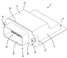
- FIG. 1 is a perspective view of the connector device of the first embodiment.
- FIG. 2 is an exploded perspective view of the connector device.
- FIG. 3 is a side sectional view showing the process of assembling the terminal holding member to the cover.
- FIG. 4 is a front view showing the process of assembling the terminal holding member to the cover.
- FIG. 5 is a side sectional view showing a state in which the terminal holding member is assembled at a normal position with respect to the cover.
- FIG. 6 is a front view showing a state in which the terminal holding member is assembled at a normal position with respect to the cover.
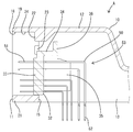
- FIG. 7 is a side sectional view showing a state in which the board connector is assembled to the cover.
- the connector device of the present disclosure is (1) A case having an opening formed on the front surface and an open lower surface, an L-shaped terminal fitting, and a board connector having a housing assembled to the opening are provided, and the terminal fitting has a front-rear direction.
- the housing has a penetrating portion extending to and a substrate connecting portion extending downward from the rear end of the penetrating portion and housed in the case, and the housing is held in a state of penetrating the penetrating portion. It has a terminal holding member that is attached to the opening from the rear and a protective member that is a separate component from the terminal holding member and is attached to the opening from the front and surrounds the front end of the penetrating portion. ing.
- the connector device of the present disclosure when assembling the board connector to the case, a protective member separated from the terminal holding member is attached to the opening from the front of the case.
- the terminal holding member is attached to the opening through the opening on the lower surface of the case. In the process of assembling the board connector, it is not necessary to pass the board connection portion located behind the terminal holding member through the opening. Therefore, the connector device of the present disclosure can prevent damage to the terminal fittings.
- the case is formed with a receiving portion protruding into the case from a part of the inner peripheral surface of the opening, and the terminal holding member is attached to the opening on the outer peripheral surface of the terminal holding member. It is preferable that a retaining portion that overlaps the front side of the receiving portion is formed when the portion is removed. According to this configuration, when the terminal holding member is attached to the opening, the retaining portion of the terminal holding member comes into contact with the front side of the receiving portion of the opening, so that the terminal holding member moves backward with respect to the opening. It is possible to prevent withdrawal.
- the protective member is formed with a pressing portion that sandwiches the retaining portion in the front-rear direction with the receiving portion. According to this configuration, when the protective member is attached to the case, the retaining portion is sandwiched between the pressing portion and the receiving portion. As a result, the terminal holding member can be fixed to the case.
- a seal member is attached between the outer peripheral surface of the protective member and the inner peripheral surface of the opening. According to this configuration, the opening can be sealed in a liquidtight manner. Since it is not necessary to provide a seal member on the outer periphery of the terminal holding member, the terminal holding member can be displaced in the vertical direction or the horizontal direction in the opening. Therefore, in designing the shape of the terminal holding member, priority can be given to ease of attachment to the opening.
- the first embodiment of the connector device A of the present disclosure will be described with reference to FIGS. 1 to 7.
- the connector device A of the first embodiment is configured by assembling a metal case 10 and a board connector 30 composed of a plurality of parts. As shown in FIG. 7, the circuit board P is attached to the connector device A.
- the front-back direction is defined as the front in FIGS. 3, 5 and 7.
- the directions appearing in FIGS. 1 to 7 are defined as upward and downward as they are.
- the directions appearing in FIGS. 4 and 6 are defined as left and right as they are.
- the case 10 has a front wall portion 11, an upper wall portion 12, left and right side wall portions 13 and a rear wall portion 14, and has a box shape in which the entire lower surface area is open.
- the open portion 15 on the lower surface of the case 10 is closed by the circuit board P.
- the left and right ends of the front wall portion 11 function as a pair of mounting portions 16.
- a female screw hole 17 having an axis directed in the front-rear direction is formed on the front surface of the mounting portion 16.
- the case 10 is formed with an opening 18 that communicates the internal space of the case 10 with the external space in front of the case 10.
- the opening 18 is a form in which a wide area between the left and right mounting portions 16 of the front wall portion 11 is opened in a square shape.
- the opening 18 is a form in which the front wall portion 11 is penetrated in the front-rear direction.
- the opening 18 has an upper edge portion 19, left and right side edge portions 20 extending downward from both left and right ends of the upper edge portion 19, and a lower edge portion 21 connecting the lower ends of the left and right side edge portions 20.
- the opening edge of the opening 18 is seamlessly connected over the entire circumference.
- a plurality of receiving portions 22 and 23 are formed on the inner peripheral surface of the opening 18.
- a pair of left and right upper edge side receiving portions 22 projecting downward are formed on the lower surface (inner surface) of the upper edge portion 19.
- a pair of side edge side receiving portions 23 are formed on the side surfaces (inner surfaces) of the left and right side edge portions 20 at intervals of the upper and lower sides, respectively.
- These receiving portions 22 and 23 are arranged at the rear end portion on the inner peripheral surface of the opening 18.
- the region of the inner peripheral surface of the opening 18 in front of the receiving portions 22 and 23 functions as the sealing surface 24.
- the board connector 30 is configured by assembling a housing 31 made of synthetic resin and a plurality of metal terminal fittings 50.
- the housing 31 includes a terminal holding member 32 and a protective member 38 which is a separate component from the terminal holding member 32.
- the terminal holding member 32 has a flat plate-shaped main body portion 33 whose plate thickness direction is directed in the front-rear direction, an upper surface portion 34, and left and right side surface portions 35.
- the upper surface portion 34 has a form extending horizontally (perpendicular to the main body portion 33) rearward from the upper edge of the main body portion 33.
- the left and right side surface portions 35 have a form extending at right angles to the rear from the left and right side edges of the main body portion 33, and are connected at right angles to the left and right side edges of the upper surface portion 34. That is, the terminal holding member 32 has a box shape in which the rear surface and the lower surface are open.
- a pair of left and right upper surface side retaining portions 36 are formed so as to project upward in a wall shape at right angles.
- a pair of upper and lower side retaining portions 37 are formed so as to project in a wall shape at right angles to the outside.
- a pair of upper and lower side retaining portions 37 are arranged vertically at intervals. The vertical dimension of the side retaining portion 37 is slightly smaller than the distance between the pair of upper and lower side edge side receiving portions 23.
- the minimum width dimension of the terminal holding member 32 in the left-right direction is slightly smaller than the distance between the left and right side edge side receiving portions 23. Is set to.
- the left-right dimension (maximum width dimension of the terminal holding member 32) from the protruding end of the left side side retaining portion 37 to the protruding end of the right side side retaining portion 37 is from the distance between the left and right side edge side receiving portions 23. Is also large, and is set to a dimension slightly smaller than the width dimension of the opening 18.
- the vertical dimension (height dimension of the terminal holding member 32) from the lower end of the main body 33 of the terminal holding member 32 to the upper end of the upper surface side retaining portion 36 is the upper edge side receiving from the upper surface of the lower edge portion 21 of the opening 18.
- the dimension is set to be slightly smaller than the vertical dimension up to the lower end of the portion 22.
- the terminal holding member 32 can be accommodated in the opening 18 from behind the opening 18 (inside the case 10).
- the upper surface side retaining portion 36 can be displaced forward from the upper edge side receiving portion 22 without interfering with the upper edge side receiving portion 22.
- the side retaining portion 37 can also be displaced forward of the side receiving portion 23 without interfering with the side edge side receiving portion 23.
- the terminal holding member 32 can be displaced upward in the opening 18 as shown in FIG.
- the upper surface side retaining portion 36 is positioned so as to face the upper edge side receiving portion 22 at the same height in the front-rear direction.
- the side retaining portion 37 is positioned so as to face the side edge side receiving portion 23 at the same height in the front-rear direction.
- the protective member 38 has a square tubular hood portion 39 penetrating in the front-rear direction and a flange portion 40 protruding from the outer periphery of the hood portion 39. As shown in FIG. 2, a pair of left and right through holes 41 penetrating in the front-rear direction are formed at both left and right ends of the flange portion 40. A metal spacer 42 is provided on the inner circumference of the through hole 41. Both the left and right through holes 41 are arranged at positions facing the female screw holes 17 of the case 10.
- the region of the hood portion 39 behind the flange portion 40 functions as the tubular fitting portion 43.
- the tubular fitting portion 43 is fitted into the opening 18.
- a seal groove 44 is formed on the outer periphery of the tubular accommodating portion, and a ring-shaped seal member 45 is mounted on the seal groove 44.
- the sealing member 45 seals between the outer peripheral surface of the tubular fitting portion 43 and the inner peripheral surface of the opening 18 in a liquidtight manner.
- the region of the terminal holding member 32 in front of the retaining portions 36 and 37 is fitted into the tubular fitting portion 43.
- the portions facing the upper surface side retaining portion 36 and the side retaining portion 37 function as the pressing portion 46.
- the terminal fitting 50 has a shape in which an elongated metal material is bent into an L shape when viewed from the side orthogonal to the front-rear direction.
- the terminal fitting 50 has a penetrating portion 51 extending in the front-rear direction and a substrate connecting portion 52 extending downward at a right angle from the rear end of the penetrating portion 51.
- the terminal fitting 50 is held by the terminal holding member 32 in a state where the penetrating portion 51 is penetrated through the main body portion 33 in the front-rear direction.
- the terminal module 53 is configured by integrating the plurality of terminal fittings 50 with the terminal holding member 32.
- the penetrating portions 51 are parallel to each other and parallel to each other, and the substrate connection portions 52 are parallel to each other and parallel to each other.
- the front end portion of the penetrating portion 51 projects forward of the main body portion 33 (terminal holding member 32).
- the rear end of the penetrating portion 51 and the entire board connecting portion 52 are exposed behind the main body portion 33.
- the lower end of the board connecting portion 52 is located below the lower end of the terminal holding member 32 (main body portion 33).
- the terminal module 53 is assembled to the case 10 in a state where the terminal holding member 32 and the protective member 38 are separated. At this time, the terminal module 53 is housed in the case 10 from the open portion 15 on the lower surface of the case 10, and the terminal holding member 32 is housed in the opening 18 from the rear.
- the moving direction of the terminal holding member 32 when the terminal holding member 32 (terminal module 53) is housed in the opening 18 is a direction parallel to the penetrating direction (front-back direction) of the opening 18.
- the height of the terminal holding member 32 is adjusted so that the upper surface side retaining portion 36 is at a position lower than the upper edge side receiving portion 22.
- the height of the terminal holding member 32 is adjusted so that the side retaining portion 37 does not interfere with the side edge side receiving portion 23. Then, as shown in FIG. 5, the terminal holding member 32 is inserted into the opening 18 until the upper surface side retaining portion 36 is located in front of the upper edge side receiving portion 22. At the same time, the terminal holding member 32 is inserted into the opening 18 until the side retaining portion 37 is located in front of the side edge side receiving portion 23.
- the terminal module 53 is displaced upward so that the upper surface side retaining portion 36 is brought into contact with the front surface of the upper edge side receiving portion 22 in a surface contact state, and the side surface side retaining portion 37 is brought into front of the side edge side receiving portion 23. In contact with the surface.
- the displacement direction of the terminal module 53 is a direction perpendicular to the penetrating direction (vertical direction) of the opening 18 and a direction parallel to the length direction of the substrate connecting portion 52.
- the terminal holding member 32 terminal module 53
- the terminal holding member 32 is attached to the case 10 at a regular assembly position. In this state, the upper surface side retaining portion 36 comes into contact with the upper edge portion 19 of the opening 18 from below.
- a square tubular shape extends over the entire circumference. Fitting space 54 is configured.
- the lower end of the board connecting portion 52 is always the lower end of the opening 18 (lower edge 21). ) Is located below. However, since the board connecting portion 52 is always located behind the opening 18 (front wall portion 11) from the start to the completion of the assembly, the board connecting portion 52 is located behind the opening 18 (front wall portion 11). It does not interfere with 11).
- the protective member 38 is assembled to the case 10.
- the protective member 38 is brought close to the front wall portion 11 from the front of the case 10, and the tubular fitting portion 43 is fitted into the opening 18 (inside the fitting space 54).
- the tubular fitting portion 43 is externally fitted to the terminal holding member 32. If the work of assembling the terminal module 53 to the case 10 and the work of assembling the protective member 38 to the case 10 are performed with the case 10, the terminal module 53, and the protective member 38 turned upside down, the workability is improved. ..
- the fitting of the case 10 is completed.
- the screw 55 is inserted into the through hole 41 from the front of the flange portion 40, and is screwed into the female screw hole 17 to be tightened.
- the assembling of the protective member 38 to the case 10 is completed, and the terminal holding member 32 and the protective member 38 are united to form the housing 31.
- the terminal module 53 and the protective member 38 are united to complete the assembly of the board connector 30, and the assembly of the board connector 30 to the case 10 is completed.
- the holding portion 46 of the protective member 38 presses the upper surface side retaining portion 36 against the upper edge side receiving portion 22 and the side retaining portion 37 against the side edge side receiving portion 23.
- the terminal holding member 32 is sandwiched between the case 10 and the protective member 38.
- the front end portions of the plurality of penetrating portions 51 are collectively surrounded by the hood portion 39 of the protective member 38.
- the board connection portion 52 is housed in the case 10.
- the lower end of the board connecting portion 52 projects downward (outside) from the open portion 15 of the case 10.
- the lower end of the board connecting portion 52 is penetrated through a through hole (not shown) of the circuit board P attached so as to close the opening portion 15 of the case 10.
- the connector device A of this embodiment includes a case 10 and a board connector 30.
- An opening 18 is formed on the front surface of the case 10.
- the lower surface of the case 10 is open to the outside.
- the board connector 30 has a plurality of terminal fittings 50 having an L shape and a housing 31 to be assembled to the opening 18.
- the terminal fitting 50 includes a penetrating portion 51 extending in the front-rear direction (direction parallel to the penetrating direction of the opening 18) and a substrate connecting portion 52 extending downward from the rear end of the penetrating portion 51 and housed in the case 10.
- the housing 31 has a terminal holding member 32 and a protective member 38.
- the terminal holding member 32 is held in a state of penetrating the penetrating portion 51, and is attached to the opening 18 from the rear.
- the protective member 38 is a separate component from the terminal holding member 32, is attached to the opening 18 from the front, and surrounds the front end portion of the penetrating portion 51.
- the protective member 38 separated from the terminal holding member 32 is attached to the opening 18 from the front of the case 10.
- the terminal holding member 32 is attached to the opening 18 through the opening on the lower surface of the case 10. Therefore, according to the connector device A of the present embodiment, it is possible to prevent the terminal fitting 50 (board connection portion 52) from being damaged due to interference with the opening 18.
- the housing 31 is separated into a protective member 38 on the hood portion 39 side and a terminal holding member 32 for holding the terminal fitting 50, and the terminal holding member 32 is contained in the case 10. I tried to accommodate only. Therefore, the case 10 can be made smaller than the case where the entire housing 31 is housed.
- the board connecting portion 52 can be brought closer to the front wall portion 11 in the attached state. As a result, it is not necessary to leave a wasted space between the front wall portion 11 and the substrate connecting portion 52, so that it is possible to prevent the case 10 from becoming large in the front-rear direction. It is possible to avoid increasing the size of the circuit board P that closes the open portion 15 on the lower surface of the case 10.
- the terminal holding member 32 can be displaced in the direction intersecting the front-rear direction (vertical direction) in the opening 18.
- the case 10 is formed with receiving portions 22 and 23 protruding into the case 10 from a part of the inner peripheral surface of the opening 18.
- Retaining portions 36 and 37 are formed on the outer peripheral surface of the terminal holding member 32. The retaining portions 36 and 37 do not interfere with the receiving portions 22 and 23 in the process of attaching the terminal holding member 32 to the opening 18.
- the retaining portions 36 and 37 overlap the front side (front surface) of the receiving portions 22 and 23.
- the retaining portions 36 and 37 can be brought into contact with the front side (front surface) of the receiving portions 22 and 23.
- the terminal holding member 32 can be positioned in the front-rear direction with respect to the case 10, and the terminal holding member 32 can be prevented from being detached rearward with respect to the opening 18.
- the protective member 38 is formed with a flange portion 40 for fixing the protective member 38 to the front surface of the case 10 and a pressing portion 46 for sandwiching the retaining portions 36 and 37 between the receiving portions 22 and 23 in the front-rear direction. ing.
- the protective member 38 is attached to the case 10 and the flange portion 40 is fixed to the front surface of the case 10, the retaining portions 36 and 37 are sandwiched between the pressing portions 46 and the receiving portions 22 and 23.
- the terminal holding member 32 is fixed to the case 10 without rattling.
- a dedicated fixing member for fixing the terminal holding member 32 to the case 10 is not required, the number of parts can be reduced.
- a seal member 45 is attached between the outer peripheral surface (seal groove 44) of the protective member 38 and the inner peripheral surface (seal surface 24) of the opening 18.
- the sealing member 45 By providing the sealing member 45, the gap between the opening 18 and the housing 31 can be sealed in a liquidtight manner. Since it is not necessary to provide the seal member 45 on the outer circumference of the terminal holding member 32, the terminal holding member 32 can be displaced in the vertical direction in the opening 18. As a result, in designing the shape of the terminal holding member 32, it is possible to set the terminal holding member 32 with priority given to the ease of attachment to the opening 18.
- the terminal holding member is fixed to the case by sandwiching the retaining portion between the holding portion and the receiving portion, but the terminal holding member may be fixed to the case by a dedicated fixing member.
- the terminal holding member is positioned in the front-rear direction with respect to the case by applying the retaining portion to the receiving portion from the front, but the portion formed on the terminal holding member is positioned from the rear with respect to the opening.
- the terminal fitting may be positioned on the case by hitting it.
- the seal member is attached to the protective member, but the seal member may be attached to the opening.
- the seal member is provided so as to be in contact with the outer peripheral surface of the protective member, but the seal member may be provided so as to be in contact with the outer peripheral surface of the terminal holding member.
- the terminal holding member can be displaced in the opening in the direction intersecting the penetration direction of the opening (vertical direction), but the terminal holding member is in the direction intersecting the penetration direction of the opening in the opening. It may not be displaced in the (vertical direction) and may be fitted from behind with respect to the opening.
- the terminal holding member is displaced in the vertical direction (direction parallel to the length direction of the substrate connection portion) in the opening, but the direction in which the terminal holding member is displaced in the opening is the horizontal direction (direction parallel to the length direction of the substrate connection portion).
- the direction that intersects the length direction of the board connection portion) may be used.
- the seal member for sealing the opening is provided, but the seal member may not be provided.
Landscapes
- Connector Housings Or Holding Contact Members (AREA)
- Coupling Device And Connection With Printed Circuit (AREA)
Abstract
端子金具の損傷を防止する。 コネクタ装置(A)は、前面に開口部(18)が形成され、下面が開放されたケース(10)と、L字形の端子金具(50)と、開口部(18)に組み付けられるハウジング(31)とを有する基板用コネクタ(30)とを備え、端子金具(50)は、前後方向に延びる貫通部(51)と、貫通部(51)の後端から下方へ延出し、ケース(10)内に収容される基板接続部(52)とを有し、ハウジング(31)は、貫通部(51)を貫通させた状態で保持し、開口部(18)に対し後方から取り付けられる端子保持部材(32)と、端子保持部材(32)とは別体部品であり、開口部(18)に対し前方から取り付けられて貫通部(51)の前端部を包囲する保護部材(38)とを有している。
Description
本開示は、コネクタ装置に関するものである。
特許文献1には、前面に方形の開口部を有するケースと、開口部に取り付けられる基板用コネクタとを有するコネクタ装置が開示されている。基板用コネクタは、ハウジングと、ハウジングに前後方向に貫通した状態で取り付けられたL字形の端子金具とを有する。端子金具は、ケース内において下向きに延出する基板接続部を有している。基板接続部の下端部は、開口部よりも下方に位置し、回路基板に接続される。ケースは、下面が開放されたケース上蓋と、ケース上蓋の下面の開放部を塞ぐケース下蓋とから構成されている。方形の開口部のうち上縁部と左右両側縁部はケース上蓋に形成され、開口部の下縁部はケース下蓋に形成されている。
基板用コネクタをケースに組み付ける際には、ケース上蓋とケース下蓋を分離して開口部を下方へ開放した形態にしておき、基板用コネクタをケース上蓋の下方から開口部に嵌合する。その後、ケース下蓋をケース上蓋に合体させ、開口部に基板用コネクタを嵌合した状態に保持する。この構造によれば、基板接続部の下端部が開口部より下方に位置していても、基板用コネクタをケースに組み付けることができる。
上記特許文献1のコネクタ装置においてケースが金属製である場合は、ケース下蓋を用いず、ケース上蓋の下面の開放部を回路基板で閉塞する構造にすると、軽量化を図ることができる。しかし、ケース下蓋を設けない構造にすると、開口部の開口縁部を全周に亘って繋げた形態にする必要がある。この場合、ケースの前方から基板用コネクタを開口部に組み付けようとすると、基板接続部の下端部が、開口部の開口縁部と干渉して損傷するおそれがある。
尚、基板接続部と開口縁部との干渉を回避する手段としては、基板用コネクタを、ケースの下面の開放部からケース内に挿入し、開口部に嵌合する構造が考えられる。しかし、基板用コネクタのフード部をケースの前方へ突出させる形態を成立させようとすると、基板用コネクタを一時的に収容するためのスペースをケース内に確保しなければならない。そのため、ケースが大型化するという新たな問題が生じる。さらには、ケースの内側から基板用コネクタを開口部にボルト締めして固定する必要がある。ケース内でドライバー等の工具で締結作業を行うのは非常に難しい。したがって、基板用コネクタをケースの下面の開放部から組み付ける方法は採用することは困難である。
本開示のコネクタ装置は、上記のような事情に基づいて完成されたものであって、端子金具の損傷を防止することを目的とする。
本開示のコネクタ装置は、
前面に開口部が形成され、下面が開放されたケースと、
L字形の端子金具と、前記開口部に組み付けられるハウジングとを有する基板用コネクタとを備え、
前記端子金具は、前後方向に延びる貫通部と、前記貫通部の後端から下方へ延出し、前記ケース内に収容される基板接続部とを有し、
前記ハウジングは、
前記貫通部を貫通させた状態で保持し、前記開口部に対し後方から取り付けられる端子保持部材と、
前記端子保持部材とは別体部品であり、前記開口部に対し前方から取り付けられて前記貫通部の前端部を包囲する保護部材とを有している。
前面に開口部が形成され、下面が開放されたケースと、
L字形の端子金具と、前記開口部に組み付けられるハウジングとを有する基板用コネクタとを備え、
前記端子金具は、前後方向に延びる貫通部と、前記貫通部の後端から下方へ延出し、前記ケース内に収容される基板接続部とを有し、
前記ハウジングは、
前記貫通部を貫通させた状態で保持し、前記開口部に対し後方から取り付けられる端子保持部材と、
前記端子保持部材とは別体部品であり、前記開口部に対し前方から取り付けられて前記貫通部の前端部を包囲する保護部材とを有している。
端子金具の損傷を防止することができる。
[本開示の実施形態の説明]
最初に本開示の実施形態を列記して説明する。
本開示のコネクタ装置は、
(1)前面に開口部が形成され、下面が開放されたケースと、L字形の端子金具と、前記開口部に組み付けられるハウジングとを有する基板用コネクタとを備え、前記端子金具は、前後方向に延びる貫通部と、前記貫通部の後端から下方へ延出し、前記ケース内に収容される基板接続部とを有し、前記ハウジングは、前記貫通部を貫通させた状態で保持し、前記開口部に対し後方から取り付けられる端子保持部材と、前記端子保持部材とは別体部品であり、前記開口部に対し前方から取り付けられて前記貫通部の前端部を包囲する保護部材とを有している。
最初に本開示の実施形態を列記して説明する。
本開示のコネクタ装置は、
(1)前面に開口部が形成され、下面が開放されたケースと、L字形の端子金具と、前記開口部に組み付けられるハウジングとを有する基板用コネクタとを備え、前記端子金具は、前後方向に延びる貫通部と、前記貫通部の後端から下方へ延出し、前記ケース内に収容される基板接続部とを有し、前記ハウジングは、前記貫通部を貫通させた状態で保持し、前記開口部に対し後方から取り付けられる端子保持部材と、前記端子保持部材とは別体部品であり、前記開口部に対し前方から取り付けられて前記貫通部の前端部を包囲する保護部材とを有している。
本開示の構成によれば、基板用コネクタをケースに組み付ける際には、端子保持部材から分離した状態の保護部材を、ケースの前方から開口部に取り付ける。端子保持部材は、ケースの下面の開口を通して開口部に取り付ける。基板用コネクタの組付けの過程において、端子保持部材の後方に位置する基板接続部を、開口部に通す必要がない。したがって、本開示のコネクタ装置は、端子金具の損傷を防止することができる。
(2)前記ケースには、前記開口部の内周面の一部からケース内に突出した受け部が形成され、前記端子保持部材の外周面には、前記端子保持部材が前記開口部に取り付けられたときに前記受け部の前方側に重なる抜止め部が形成されていることが好ましい。この構成によれば、端子保持部材を開口部に取り付けた状態では、端子保持部材の抜止め部が開口部の受け部の前方側に当接するので、端子保持部材が開口部に対して後方へ離脱することを防止できる。
(3)(2)において、前記保護部材に、前記受け部との間で前記抜止め部を前後方向に挟み付ける押え部が形成されていることが好ましい。この構成によれば、保護部材をケースに取り付けると、抜止め部が押え部と受け部との間で挟み付けられる。これにより、端子保持部材をケースに固定することができる。
(4)前記保護部材の外周面と前記開口部の内周面との間には、シール部材が取り付けられていることが好ましい。この構成によれば、開口部を液密状にシールすることができる。端子保持部材の外周にシール部材を設ける必要がないので、端子保持部材を開口部内で上下方向や左右方向へ変位させることが可能となる。したがって、端子保持部材の形状の設計において開口部への取付け易さを優先することができる。
[本開示の実施形態の詳細]
[実施例1]
本開示のコネクタ装置Aを具体化した実施例1を、図1~図7を参照して説明する。本実施例1のコネクタ装置Aは、金属製のケース10と、複数の部品からなる基板用コネクタ30とを組み付けて構成されている。図7に示すように、コネクタ装置Aには回路基板Pが取り付けられるようになっている。本実施例1において、前後の方向については、図3,5,7における左方を前方と定義する。上下の方向については、図1~7にあらわれる向きを、そのまま上方、下方と定義する。左右の方向については、図4,6にあらわれる向きを、そのまま左方、右方と定義する。
[実施例1]
本開示のコネクタ装置Aを具体化した実施例1を、図1~図7を参照して説明する。本実施例1のコネクタ装置Aは、金属製のケース10と、複数の部品からなる基板用コネクタ30とを組み付けて構成されている。図7に示すように、コネクタ装置Aには回路基板Pが取り付けられるようになっている。本実施例1において、前後の方向については、図3,5,7における左方を前方と定義する。上下の方向については、図1~7にあらわれる向きを、そのまま上方、下方と定義する。左右の方向については、図4,6にあらわれる向きを、そのまま左方、右方と定義する。
ケース10は、前壁部11と上壁部12と左右両側壁部13と後壁部14とを有し、下面の全領域が開放された箱形をなす。ケース10の下面の開放部15は回路基板Pによって閉塞されるようになっている。前壁部11の左右両端部は、一対の取付部16として機能する。取付部16の前面には、軸線を前後方向に向けた雌ネジ孔17が形成されている。
ケース10には、ケース10の内部空間とケース10の前方の外部空間とを連通させる開口部18が形成されている。開口部18は、前壁部11のうち左右両取付部16の間の広い領域を方形に開口させた形態である。換言すると、開口部18は前壁部11を前後方向に貫通させた形態である。開口部18は、上縁部19と、上縁部19の左右両端から下方へ延出した左右両側縁部20と、左右両側縁部20の下端同士を連結する下縁部21とを有する。開口部18の開口縁部は全周に亘って切れ目なく繋がっている。
開口部18の内周面には、複数の受け部22,23が形成されている。上縁部19の下面(内面)には、下向きに突出する左右一対の上縁側受け部22が形成されている。左右両側縁部20の側面(内面)には、それぞれ、上下に間隔を空けた一対ずつの側縁側受け部23が形成されている。これらの受け部22,23は、開口部18の内周面における後端部に配されている。開口部18の内周面のうち受け部22,23よりも前方の領域は、シール面24として機能する。
基板用コネクタ30は、合成樹脂製のハウジング31と、金属製の複数の端子金具50とを組み付けて構成されている。ハウジング31は、端子保持部材32と、端子保持部材32とは別体部品である保護部材38とを備えて構成されている。端子保持部材32は、板厚方向を前後方向に向けた平板状の本体部33と、上面部34と、左右両側面部35とを有する。上面部34は、本体部33の上縁から後方へ水平に(本体部33と直角に)延出した形態である。左右両側面部35は、本体部33の左右両側縁から後方へ直角に延出した形態であり、上面部34の左右両側縁に対し直角に連なっている。つまり、端子保持部材32は、後面と下面が開放された箱状をなしている。
上面部34の外面(上面)における後端部には、上方へ直角に壁状に突出した形態の左右一対の上面側抜止め部36が形成されている。左右両側面部35の外面(外側面)における後端部には、それぞれ、外側方へ直角に壁状に突出した形態の上下一対ずつの側面側抜止め部37が形成されている。上下一対の側面側抜止め部37は、上下に間隔を空けて配置されている。側面側抜止め部37の上下寸法は、上下一対の側縁側受け部23の間隔よりも僅かに小さい寸法である。
端子保持部材32の左右方向の最小幅寸法(左側の側面部35の外面と右側の側面部35の外面との間の距離)は、左右の側縁側受け部23の間隔よりも僅かに小さい寸法に設定されている。左側の側面側抜止め部37の突出端から右側の側面側抜止め部37の突出端までの左右方向の寸法(端子保持部材32の最大幅寸法)は、左右両側縁側受け部23の間隔よりも大きく、開口部18の幅寸法よりも僅かに小さい寸法に設定されている。端子保持部材32の本体部33の下端から上面側抜止め部36の上端までの上下寸法(端子保持部材32の高さ寸法)は、開口部18の下縁部21の上面から、上縁側受け部22の下端までの上下寸法よりも僅かに小さい寸法に設定されている。
かかる寸法設定としたことにより、端子保持部材32は、開口部18の後方(ケース10の内部)から開口部18内に収容することができる。このとき、端子保持部材32を開口部18内に収容する過程では、上面側抜止め部36は、上縁側受け部22と干渉せずに上縁側受け部22よりも前方へ変位することができる。また、側面側抜止め部37も、側縁側受け部23と干渉することなく、側縁側受け部23よりも前方へ変位することができる。
また、抜止め部36,37が受け部22,23よりも前方に位置する状態では、図6に示すように、端子保持部材32を開口部18内で上方へ変位させることができる。端子保持部材32を開口部18内で上方へ変位させると、上面側抜止め部36が上縁側受け部22と同じ高さで前後方向に対向するように位置する。端子保持部材32を開口部18内で上方へ変位させると、側面側抜止め部37が、側縁側受け部23と同じ高さで前後方向に対向するように位置する。
保護部材38は、前後方向に貫通した角筒状のフード部39と、フード部39の外周から張り出したフランジ部40とを有する。図2に示すように、フランジ部40の左右両端部には、前後方向に貫通した形態の左右一対の貫通孔41が形成されている。貫通孔41の内周には金属製のスペーサ42が設けられている。左右両貫通孔41は、ケース10の雌ネジ孔17と対向する位置に配されている。
図7に示すように、フード部39のうちフランジ部40よりも後方の領域は、筒状嵌合部43として機能する。筒状嵌合部43は、開口部18に内嵌されるようになっている。筒状収容部の外周にはシール溝44が形成され、シール溝44にはリング状のシール部材45が装着されている。筒状嵌合部43を開口部18に嵌合した状態では、シール部材45が筒状嵌合部43の外周面と開口部18の内周面との間を液密状にシールする。筒状嵌合部43には、端子保持部材32のうち抜止め部36,37よりも前方の領域が嵌入されるようになっている。筒状嵌合部43の後端部のうち上面側抜止め部36及び側面側抜止め部37と対向する部位は、押え部46として機能する。
端子金具50は、前後方向と直交する側方から視た側面視において、細長い金属素材をL字形に屈曲した形状をなす。端子金具50は、前後方向に延びる貫通部51と、貫通部51の後端から下方へ直角に延出した基板接続部52とを有する。端子金具50は、貫通部51を本体部33に前後方向に貫通させた状態で端子保持部材32に保持されている。複数の端子金具50を端子保持部材32に一体化させることにより、端子モジュール53が構成されている。
複数の端子金具50を端子保持部材32に保持した状態では、貫通部51同士が互いに平行をなして並列し、基板接続部52同士が互いに平行をなして並列する。貫通部51の前端部は、本体部33(端子保持部材32)の前方へ突出する。貫通部51の後端部と基板接続部52の全体は、本体部33の後方に露出している。基板接続部52の下端部は、端子保持部材32(本体部33)の下端よりも下方に位置している。
次に、コネクタ装置Aの組み付け手順を説明する。まず、端子保持部材32と保護部材38を分離した状態で、端子モジュール53をケース10に組み付ける。このとき、端子モジュール53をケース10の下面の開放部15からケース10内に収容し、端子保持部材32を後方から開口部18内に収容する。端子保持部材32(端子モジュール53)を開口部18内に収容するときの端子保持部材32の移動方向は、開口部18の貫通方向(前後方向)と平行な方向である。図4に示すように、上面側抜止め部36が上縁側受け部22よりも低い位置となるように、端子保持部材32の高さを調整する。同時に、側面側抜止め部37が側縁側受け部23と干渉しないように、端子保持部材32の高さを調整する。そして、図5に示すように、上面側抜止め部36が上縁側受け部22よりも前方に位置するまで、端子保持部材32を開口部18内に挿入する。同時に、側面側抜止め部37が側縁側受け部23よりも前方に位置するまで、端子保持部材32を開口部18内に挿入する。
この後、端子モジュール53を上方へ変位させ、上面側抜止め部36を上縁側受け部22の前面に面当たり状態で当接させるとともに、側面側抜止め部37を側縁側受け部23に前面に面当たり状態で当接させる。このときの、端子モジュール53(端子保持部材32)の変位方向は、開口部18の貫通方向(上下方向)と直角な方向であり、基板接続部52の長さ方向と平行に方向である。以上により、端子保持部材32(端子モジュール53)がケース10に対して正規の組付位置に取り付けられる。この状態では、上面側抜止め部36が開口部18の上縁部19に対し下から当接する。図5,6に示すように、端子保持部材32のうち抜止め部36,37よりも前方の領域の外周と、開口部18の内周との間には、全周に亘って角筒状の嵌合空間54が構成される。
上記のように開口部18に対する端子モジュール53の組付けを開始してから、組付けが完了するまでの間、基板接続部52の下端部は、常に、開口部18の下端(下縁部21)よりも下方に位置する。しかし、組み付けの開始から完了に至るまでの間、基板接続部52は、常に、開口部18(前壁部11)よりも後方に位置するので、基板接続部52が開口部18(前壁部11)と干渉することはない。
端子モジュール53をケース10に組み付けた後は、保護部材38をケース10に組み付ける。このとき、保護部材38をケース10の前方から前壁部11に接近させ、筒状嵌合部43を開口部18内(嵌合空間54内)に嵌入する。これに伴い、筒状嵌合部43が端子保持部材32に外嵌される。尚、端子モジュール53をケース10に組み付ける作業と、保護部材38をケース10に組み付ける作業は、ケース10と端子モジュール53と保護部材38を上下反転させた状態で行うと、作業性が良好となる。
フランジ部40が前壁部11の前面に当接すると、ケース10の嵌合が完了する。この後、フランジ部40の前方からビス55を貫通孔41に挿通し、雌ネジ孔17にねじ込んで締め付ける。以上により、ケース10に対する保護部材38の組付けが完了し、端子保持部材32と保護部材38が合体してハウジング31が構成される。端子モジュール53と保護部材38が合体して基板用コネクタ30の組付けが完了し、ケース10に対する基板用コネクタ30の組付けが完了する。
ビス55を締め付けると、保護部材38の押え部46が、上面側抜止め部36を上縁側受け部22に押し付けるとともに、側面側抜止め部37を側縁側受け部23に押し付ける。この押え部46による押し付けにより、端子保持部材32は、ケース10と保護部材38との間に挟み付けられる。この挟み付けにより、端子保持部材32は、ケース10と保護部材38に対してがたつきを規制された状態に固定される。複数の貫通部51の前端部は、保護部材38のフード部39により一括して包囲される。基板接続部52はケース10内に収容される。基板接続部52の下端部は、ケース10の開放部15からケース10の下方(外部)へ突出している。基板接続部52の下端部は、ケース10の開放部15を閉塞するように取り付けられた回路基板Pのスルーホール(図示省略)に貫通される。
本実施例のコネクタ装置Aは、ケース10と基板用コネクタ30とを備えている。ケース10の前面には開口部18が形成されている。ケース10の下面は外部に開放されている。基板用コネクタ30は、L字形をなす複数の端子金具50と、開口部18に組み付けられるハウジング31とを有している。端子金具50は、前後方向(開口部18の貫通方向と平行に方向)に延びる貫通部51と、貫通部51の後端から下方へ延出し、ケース10内に収容される基板接続部52とを有する。ハウジング31は、端子保持部材32と保護部材38とを有する。端子保持部材32は、貫通部51を貫通させた状態で保持し、開口部18に対し後方から取り付けられるようになっている。保護部材38は、端子保持部材32とは別体部品であり、開口部18に対し前方から取り付けられて貫通部51の前端部を包囲する。
基板用コネクタ30をケース10に組み付ける際には、端子保持部材32から分離した状態の保護部材38を、ケース10の前方から開口部18に取り付ける。端子保持部材32は、ケース10の下面の開口を通して開口部18に取り付ける。基板用コネクタ30をケース10に組み付ける過程において、端子保持部材32の後方に位置する基板接続部52を、開口部18に通す必要がない。したがって、本実施例のコネクタ装置Aによれば、端子金具50(基板接続部52)が開口部18と干渉することに起因して損傷することを防止できる。
基板接続部52と開口部18との干渉を回避する手段としては、基板用コネクタ30を、ケース10の下面の開放部15からケース10内に挿入して、開口部18に嵌合する構造が考えられる。しかし、基板用コネクタ30のフード部39をケース10の前方へ突出させる形態を成立させようとすると、基板用コネクタ30を一時的に収容するためのスペースをケース10内に確保しなければならない。そのため、ケース10が大型化するという新たな問題が生じる。さらには、ケース10の内側から基板用コネクタ30を開口部18にボルト締めして固定する必要がある。ケース10内でドライバー等の工具で締結作業を行うのは非常に難しい。したがって、基板用コネクタ30をケース10の下面の開放部15から組み付ける方法は、好ましくない。
これに対し、本実施例のコネクタ装置Aは、ハウジング31をフード部39側の保護部材38と、端子金具50を保持する端子保持部材32とに分離し、ケース10内には端子保持部材32だけを収容するようにした。したがって、ハウジング31全体を収容する場合に比べると、ケース10を小型化することができた。
また、端子保持部材32は、前壁部11の後方から平行移動させながら開口部18に取り付けるので、取り付け状態では基板接続部52を前壁部11に接近させることができる。これにより、前壁部11と基板接続部52との間に無駄な空間が空かずに済むので、ケース10が前後方向に大型化するのを回避できる。ケース10の下面の開放部15を閉塞する回路基板Pに関しても、大型化することを回避できる。
端子保持部材32は、前記開口部18内において前後方向と交差する方向(上下方向)への変位が可能となっている。ケース10には、開口部18の内周面の一部からケース10内に突出した受け部22,23が形成されている。端子保持部材32の外周面には、抜止め部36,37が形成されている。抜止め部36,37は、端子保持部材32を開口部18に取り付ける過程では受け部22,23と干渉しない。端子保持部材32が開口部18に対して正規の取付け位置にあるときに、抜止め部36,37が受け部22,23の前方側(前面)に重なるようになっている。
この構成によれば、端子保持部材32を開口部18に取り付けると、抜止め部36,37を受け部22,23の前方側(前面)に当接させることができる。これにより、端子保持部材32をケース10に対して前後方向に位置決めできるとともに、端子保持部材32が開口部18に対して後方へ離脱することを防止できる。
保護部材38には、保護部材38をケース10の前面に固定するフランジ部40と、受け部22,23との間で抜止め部36,37を前後方向に挟み付ける押え部46とが形成されている。保護部材38をケース10に取り付けてフランジ部40をケース10の前面に固定すると、抜止め部36,37が、押え部46と受け部22,23との間で挟み付けられる。これにより、端子保持部材32がケース10に対してガタ付きなく固定される。また、端子保持部材32をケース10に固定するための専用の固定部材が不要なので、部品点数を削減できる。
保護部材38の外周面(シール溝44)と開口部18の内周面(シール面24)との間には、シール部材45が取り付けられている。シール部材45を設けたことにより、開口部18とハウジング31との隙間を液密状にシールすることができる。端子保持部材32の外周にシール部材45を設ける必要がないので、端子保持部材32を開口部18内で上下方向へ変位させることが可能となっている。これにより、端子保持部材32の形状の設計において、開口部18への取付け易さを優先して端子保持部材32の設定を行うことが可能となった。
[他の実施例]
本発明は、上記記述及び図面によって説明した実施例に限定されるものではなく、特許請求の範囲によって示される。本発明には、特許請求の範囲と均等の意味及び特許請求の範囲内でのすべての変更が含まれ、下記のような実施形態も含まれることが意図される。
上記実施例では、抜止め部を押え部と受け部との間で挟むことにより、端子保持部材をケースに固定したが、専用の固定部材によって端子保持部材をケースに固定してもよい。
上記実施例では、抜止め部を前方から受け部に当てることにより、端子保持部材がケースに対して前後方向に位置決めされているが、端子保持部材に形成した部位を開口部に対して後方から当てることによって、端子金具をケースに位置決めしてもよい。
上記実施例では、シール部材を保護部材に取り付けたが、シール部材は開口部に取り付けてもよい。
上記実施例では、シール部材を保護部材の外周面に接するように設けたが、シール部材は、端子保持部材の外周面に接するように設けてもよい。
上記実施例では、端子保持部材が開口部内において開口部の貫通方向と交差する方向(上下方向)へ変位できるようにしたが、端子保持部材は、開口部内において開口部の貫通方向と交差する方向(上下方向)へ変位できず、開口部に対して後方から嵌合されるようにしてもよい。
上記実施例では、端子保持部材が開口部内で上下方向(基板接続部の長さ方向と平行な方向)へ変位するようにしたが、開口部内で端子保持部材が変位する方向は、左右方向(基板接続部の長さ方向と交差する方向)でもよい。
上記実施例では、開口部をシールするためのシール部材を設けたが、シール部材を有しない形態としてもよい。
A:コネクタ装置
P:回路基板
10:ケース
11:前壁部
12:上壁部
13:側壁部
14:後壁部
15:開放部
16:取付部
17:雌ネジ孔
18:開口部
19:上縁部
20:側縁部
21:下縁部
22:上縁側受け部(受け部)
23:側縁側受け部(受け部)
24:シール面
30:基板用コネクタ
31:ハウジング
32:端子保持部材
33:本体部
34:上面部
35:側面部
36:上面側抜止め部(抜止め部)
37:側面側抜止め部(抜止め部)
38:保護部材
39:フード部
40:フランジ部(固定部)
41:貫通孔
42:スペーサ
43:筒状嵌合部
44:シール溝
45:シール部材
46:押え部
50:端子金具
51:貫通部
52:基板接続部
53:端子モジュール
54:嵌合空間
55:ビス
Claims (4)
- 前面に開口部が形成され、下面が開放されたケースと、
L字形の端子金具と、前記開口部に組み付けられるハウジングとを有する基板用コネクタとを備え、
前記端子金具は、
前後方向に延びる貫通部と、
前記貫通部の後端から下方へ延出し、前記ケース内に収容される基板接続部とを有し、
前記ハウジングは、
前記貫通部を貫通させた状態で保持し、前記開口部に対し後方から取り付けられる端子保持部材と、
前記端子保持部材とは別体部品であり、前記開口部に対し前方から取り付けられて前記貫通部の前端部を包囲する保護部材とを有しているコネクタ装置。 - 前記ケースには、前記開口部の内周面の一部からケース内に突出した受け部が形成され、
前記端子保持部材の外周面には、前記端子保持部材が前記開口部に取り付けられたときに前記受け部の前方側に重なる抜止め部が形成されている請求項1に記載のコネクタ装置。 - 前記保護部材に、前記受け部との間で前記抜止め部を前後方向に挟み付ける押え部が形成されている請求項2に記載のコネクタ装置。
- 前記保護部材の外周面と前記開口部の内周面との間には、シール部材が取り付けられている請求項1から請求項3のいずれか1項に記載のコネクタ装置。
Priority Applications (2)
| Application Number | Priority Date | Filing Date | Title |
|---|---|---|---|
| US17/617,549 US12212085B2 (en) | 2019-06-21 | 2020-06-02 | Connector device having case and board connector |
| CN202080044345.0A CN114008865B (zh) | 2019-06-21 | 2020-06-02 | 连接器装置 |
Applications Claiming Priority (2)
| Application Number | Priority Date | Filing Date | Title |
|---|---|---|---|
| JP2019-115274 | 2019-06-21 | ||
| JP2019115274A JP7131495B2 (ja) | 2019-06-21 | 2019-06-21 | コネクタ装置 |
Publications (1)
| Publication Number | Publication Date |
|---|---|
| WO2020255695A1 true WO2020255695A1 (ja) | 2020-12-24 |
Family
ID=73995517
Family Applications (1)
| Application Number | Title | Priority Date | Filing Date |
|---|---|---|---|
| PCT/JP2020/021679 Ceased WO2020255695A1 (ja) | 2019-06-21 | 2020-06-02 | コネクタ装置 |
Country Status (4)
| Country | Link |
|---|---|
| US (1) | US12212085B2 (ja) |
| JP (1) | JP7131495B2 (ja) |
| CN (1) | CN114008865B (ja) |
| WO (1) | WO2020255695A1 (ja) |
Families Citing this family (2)
| Publication number | Priority date | Publication date | Assignee | Title |
|---|---|---|---|---|
| WO2019244511A1 (ja) * | 2018-06-19 | 2019-12-26 | 株式会社オートネットワーク技術研究所 | 電気接続箱 |
| JP7240616B2 (ja) * | 2020-09-24 | 2023-03-16 | 住友電装株式会社 | コネクタ |
Citations (3)
| Publication number | Priority date | Publication date | Assignee | Title |
|---|---|---|---|---|
| JPH0315483U (ja) * | 1989-06-28 | 1991-02-15 | ||
| JP2007234429A (ja) * | 2006-03-01 | 2007-09-13 | Denso Corp | コネクタの実装構造及び電子装置 |
| JP2015041725A (ja) * | 2013-08-23 | 2015-03-02 | 三菱電機株式会社 | 電子制御装置及びその製造方法 |
Family Cites Families (21)
| Publication number | Priority date | Publication date | Assignee | Title |
|---|---|---|---|---|
| US6407925B1 (en) * | 1999-09-17 | 2002-06-18 | Denso Corporation | Casing for electronic control devices |
| JP3954977B2 (ja) * | 2003-03-11 | 2007-08-08 | 矢崎総業株式会社 | 電子ユニット |
| JP3984579B2 (ja) * | 2003-09-16 | 2007-10-03 | 株式会社オートネットワーク技術研究所 | インバータ用コネクタ装置 |
| US7118646B2 (en) * | 2004-03-15 | 2006-10-10 | Delphi Technologies, Inc. | Method of manufacturing a sealed electronic module |
| JP2006012545A (ja) * | 2004-06-24 | 2006-01-12 | Keihin Corp | コネクタの保持構造 |
| JP2006066207A (ja) * | 2004-08-26 | 2006-03-09 | Sumitomo Wiring Syst Ltd | 基板用コネクタのシールド構造 |
| JP2007335297A (ja) * | 2006-06-16 | 2007-12-27 | Japan Aviation Electronics Industry Ltd | 基板用コネクタ |
| US7201587B1 (en) * | 2006-07-31 | 2007-04-10 | Delphi Technologies, Inc. | Electrical connector with right angle terminal pins |
| JP5038412B2 (ja) * | 2007-11-29 | 2012-10-03 | 日本特殊陶業株式会社 | 金属樹脂複合体 |
| WO2009093424A1 (ja) * | 2008-01-24 | 2009-07-30 | Mitsubishi Cable Industries, Ltd. | 電気コネクタ付回路基板用ケース及びそれを備えた電子ユニット |
| EP2083555A3 (en) * | 2008-01-28 | 2011-09-07 | Tyco Electronics AMP Korea Limited | Waterproofing method and structure for mobile phone |
| JP2012231004A (ja) * | 2011-04-26 | 2012-11-22 | Honda Elesys Co Ltd | 導通端子半田ストレス防止構造 |
| JP5526096B2 (ja) * | 2011-09-21 | 2014-06-18 | 日立オートモティブシステムズ株式会社 | 電子制御装置のシール構造 |
| JP5358639B2 (ja) * | 2011-09-21 | 2013-12-04 | 日立オートモティブシステムズ株式会社 | 電子制御装置のシール構造 |
| JP5880428B2 (ja) * | 2012-12-28 | 2016-03-09 | 株式会社オートネットワーク技術研究所 | カードエッジコネクタ |
| JP6183233B2 (ja) * | 2014-01-30 | 2017-08-23 | 株式会社オートネットワーク技術研究所 | カードエッジコネクタ |
| US9293870B1 (en) * | 2015-03-10 | 2016-03-22 | Continental Automotive Systems, Inc. | Electronic control module having a cover allowing for inspection of right angle press-fit pins |
| US9882295B2 (en) * | 2015-09-07 | 2018-01-30 | Yazaki Corporation | Connector |
| JP2017195041A (ja) * | 2016-04-19 | 2017-10-26 | 日本圧着端子製造株式会社 | コネクタ及びコネクタ付きユニット |
| JP6737011B2 (ja) * | 2016-07-01 | 2020-08-05 | 株式会社オートネットワーク技術研究所 | シールドコネクタ |
| JP6785261B2 (ja) * | 2018-05-11 | 2020-11-18 | 矢崎総業株式会社 | コネクタユニット |
-
2019
- 2019-06-21 JP JP2019115274A patent/JP7131495B2/ja active Active
-
2020
- 2020-06-02 CN CN202080044345.0A patent/CN114008865B/zh active Active
- 2020-06-02 WO PCT/JP2020/021679 patent/WO2020255695A1/ja not_active Ceased
- 2020-06-02 US US17/617,549 patent/US12212085B2/en active Active
Patent Citations (3)
| Publication number | Priority date | Publication date | Assignee | Title |
|---|---|---|---|---|
| JPH0315483U (ja) * | 1989-06-28 | 1991-02-15 | ||
| JP2007234429A (ja) * | 2006-03-01 | 2007-09-13 | Denso Corp | コネクタの実装構造及び電子装置 |
| JP2015041725A (ja) * | 2013-08-23 | 2015-03-02 | 三菱電機株式会社 | 電子制御装置及びその製造方法 |
Also Published As
| Publication number | Publication date |
|---|---|
| CN114008865B (zh) | 2024-05-14 |
| US20220247106A1 (en) | 2022-08-04 |
| CN114008865A (zh) | 2022-02-01 |
| JP7131495B2 (ja) | 2022-09-06 |
| US12212085B2 (en) | 2025-01-28 |
| JP2021002462A (ja) | 2021-01-07 |
Similar Documents
| Publication | Publication Date | Title |
|---|---|---|
| JP6135516B2 (ja) | 機器用コネクタ | |
| JP6531628B2 (ja) | ケースの閉止構造 | |
| JP5394201B2 (ja) | 画像表示装置 | |
| CN108352651B (zh) | 密封盖 | |
| JP2019197640A (ja) | 防水コネクタ及び機器ケースの防水構造 | |
| US20180109027A1 (en) | Waterproof electronic control device | |
| CN114521311A (zh) | 电气插头连接器 | |
| CN107706582B (zh) | 摄像装置 | |
| JP2021002462A (ja) | コネクタ装置 | |
| JP5244055B2 (ja) | 遊技機用の制御基板収納ケース | |
| JP7132204B2 (ja) | 電気接続箱 | |
| JP2015046483A (ja) | 防水筐体 | |
| JP5716647B2 (ja) | 電子装置 | |
| WO2021206131A1 (ja) | コネクタユニットおよびワイヤハーネス | |
| JP6446525B1 (ja) | 配線用グロメット | |
| JP4718891B2 (ja) | 電気接続箱 | |
| JP6497148B2 (ja) | カバー付筐体の製造方法 | |
| JP4387128B2 (ja) | 遊技機の制御装置 | |
| JP2017212107A (ja) | アース端子の取付構造、及び、電線収容体 | |
| JP4931132B2 (ja) | 電気電子機器収納用箱のアース端子構造 | |
| JP7077129B2 (ja) | 筐体へのコネクタ組立体の取付構造 | |
| JP5692350B1 (ja) | 電気コネクタの取付構造 | |
| JP6019158B1 (ja) | 遊技機の筐体 | |
| JP5682696B1 (ja) | 電気コネクタの取付構造 | |
| TWI744461B (zh) | 殼體組件、電子組件模組及具有電子組件模組的電子裝置 |
Legal Events
| Date | Code | Title | Description |
|---|---|---|---|
| 121 | Ep: the epo has been informed by wipo that ep was designated in this application |
Ref document number: 20825454 Country of ref document: EP Kind code of ref document: A1 |
|
| NENP | Non-entry into the national phase |
Ref country code: DE |
|
| 122 | Ep: pct application non-entry in european phase |
Ref document number: 20825454 Country of ref document: EP Kind code of ref document: A1 |