WO2020198168A1 - Receiver combining for hybrid analog-digital beamforming - Google Patents
Receiver combining for hybrid analog-digital beamforming Download PDFInfo
- Publication number
- WO2020198168A1 WO2020198168A1 PCT/US2020/024318 US2020024318W WO2020198168A1 WO 2020198168 A1 WO2020198168 A1 WO 2020198168A1 US 2020024318 W US2020024318 W US 2020024318W WO 2020198168 A1 WO2020198168 A1 WO 2020198168A1
- Authority
- WO
- WIPO (PCT)
- Prior art keywords
- matrix
- digital
- analog
- fully
- combiner
- Prior art date
- Legal status (The legal status is an assumption and is not a legal conclusion. Google has not performed a legal analysis and makes no representation as to the accuracy of the status listed.)
- Ceased
Links
Classifications
-
- H—ELECTRICITY
- H04—ELECTRIC COMMUNICATION TECHNIQUE
- H04B—TRANSMISSION
- H04B7/00—Radio transmission systems, i.e. using radiation field
- H04B7/02—Diversity systems; Multi-antenna system, i.e. transmission or reception using multiple antennas
- H04B7/04—Diversity systems; Multi-antenna system, i.e. transmission or reception using multiple antennas using two or more spaced independent antennas
- H04B7/08—Diversity systems; Multi-antenna system, i.e. transmission or reception using multiple antennas using two or more spaced independent antennas at the receiving station
- H04B7/0837—Diversity systems; Multi-antenna system, i.e. transmission or reception using multiple antennas using two or more spaced independent antennas at the receiving station using pre-detection combining
- H04B7/084—Equal gain combining, only phase adjustments
-
- H—ELECTRICITY
- H04—ELECTRIC COMMUNICATION TECHNIQUE
- H04B—TRANSMISSION
- H04B7/00—Radio transmission systems, i.e. using radiation field
- H04B7/02—Diversity systems; Multi-antenna system, i.e. transmission or reception using multiple antennas
- H04B7/04—Diversity systems; Multi-antenna system, i.e. transmission or reception using multiple antennas using two or more spaced independent antennas
- H04B7/08—Diversity systems; Multi-antenna system, i.e. transmission or reception using multiple antennas using two or more spaced independent antennas at the receiving station
- H04B7/0837—Diversity systems; Multi-antenna system, i.e. transmission or reception using multiple antennas using two or more spaced independent antennas at the receiving station using pre-detection combining
- H04B7/0842—Weighted combining
- H04B7/086—Weighted combining using weights depending on external parameters, e.g. direction of arrival [DOA], predetermined weights or beamforming
Definitions
- Massive-MIMO Multiple Input Multiple Output
- RX RF receiver radio frequency
- a hybrid beamforming method includes: obtaining a multiple input multiple output (MIMO) signal combiner matrix; decomposing the MIMO signal combiner matrix into a first and a second constituent matrix, the combiner matrix being a scaled sum of the first and second constituent matrices.
- the MIMO signal combiner matrix is single user MIMO (SU MIMO) matrix, or a multi-user MIMO (MU MIMO) matrix.
- the SU MIMO signal combiner may be calculated using a singular value decomposition algorithm, and may also include calculating a precoding matrix, P, while the MU MIMO matrix may be obtained using either a zero-forcing algorithm or a minimum mean squared error algorithm, or other suitable algorithm.
- Additional embodiments may include: processing a set of receive-antenna signals using the first constituent matrix to obtain a first intermediate received signal vector; processing the set of receive- antenna signals using the second constituent matrix to obtain a second intermediate received signal vector; and, forming a set of received signals by adding corresponding elements of the first and second intermediate signal vectors.
- the set of received signals is also formed by applying a scaling factor either to the first and second intermediate signal vectors, or to the sum of the corresponding elements of the first and second intermediate signal vectors.
- the first and second constituent matrices are formed by offsetting the angles of MIMO signal combiner matrix.
- a method includes decomposing a fully-digital combiner into a product of two matrices, representing analog and digital precoders, where the analog precoder requires only N s RF chains.
- the dimensions of analog and digital combiners are N R x N s and N s x N s , respectively.
- the fully-digital combiner is W FD is formed in accordance with , where is the analog combiner and W D is the digital precoder, and the analog precoder has constituent matrices W
- the digital combiner of the hybrid beamformer may be any arbitrary
- the digital combiner is: W
- the receive hybrid combiner is given as:
- an apparatus includes a radio frequency (RF) analog signal processing (ASP) network, having N input and M output ports, comprising feed-forward connections of T RF components, the RF components selected from the group comprising phase-shifters, power combiners and power dividers.
- RF radio frequency
- ASP analog signal processing
- an apparatus includes an ASP representing a given matrix comprising N dividers, M combiners, and 2NM phase-shifters.
- an apparatus includes: a plurality of signal splitters, each signal splitter configured to process a signal received from an antenna element and to generate a set of power- divided output signals; a plurality of sets of configurable phase shifters, each set of configurable phase shifters operating on a respective set of power-divided output signals to generate sets of phase-shifted power-divided output signals; and a plurality of signal combiners, each signal combiner receiving a plurality of phase-shifted power-divided output signals and providing a combined output signal.
- a method includes processing a plurality of signals using a radio frequency (RF) analog signal processing (ASP) network, having N input and M output ports, comprising feed-forward connections of T RF components, the RF components selected from the group comprising phase-shifters, power combiners and power dividers.
- RF radio frequency
- ASP analog signal processing
- a method includes configuring an ASP comprising N dividers,
- a method includes: processing a signal received from an antenna element using a plurality of signal splitters, each signal splitter configured to generate a set of power-divided output signals; operating on a respective set of power-divided output signals using a plurality of sets of configurable phase shifters, each set of configurable phase shifters configured to generate sets of phase-shifted power-divided output signals; and receiving a plurality of phase-shifted power-divided output signals at a plurality of signal combiners, each signal combiner providing a combined output signal.
- FIG. 1 A is a system diagram illustrating an example communications system in which one or more disclosed embodiments may be implemented
- FIG. 1 B is a system diagram illustrating an example wireless transmit/receive unit (WTRU) that may be used within the communications system illustrated in FIG. 1A according to an embodiment;
- WTRU wireless transmit/receive unit
- FIG. 1 C is a system diagram illustrating an example radio access network (RAN) and an example core network (CN) that may be used within the communications system illustrated in FIG. 1 A according to an embodiment;
- RAN radio access network
- CN core network
- FIG. 1 D is a system diagram illustrating a further example RAN and a further example CN that may be used within the communications system illustrated in FIG. 1A according to an embodiment
- FIG. 2 illustrates a typical mmWave massive-MIMO receiver with hybrid analog/digital beamforming
- FIG. 3 graphically illustrates an example annulus in a complex plane, in accordance with some embodiments
- FIG. 4 illustrates an example hybrid analog/digital structure, in accordance with some embodiments
- FIG. 5 graphically illustrates an example of a bit error rate (BER) versus signal-to-noise ratio (SNR) for a single user (SU) scenario, accordance with some embodiments.
- BER bit error rate
- SNR signal-to-noise ratio
- FIG. 6 graphically illustrates an example of a bit error rate (BER) versus signa-to-noise ratio (SNR) for a multi-user (MU) scenario, accordance with some embodiments.
- BER bit error rate
- SNR signa-to-noise ratio
- FIG. 7 illustrates a conventional HSP architecture for a single user massive-MIMO system.
- FIG. 8 illustrates an example of a generalized FISP-based massive-MIMO transmitter, in accordance with some embodiments.
- FIG. 9 illustrates an example of a generalized HSP-based massive-MIMO receiver, in accordance with some embodiments.
- FIG. 10A illustrates an example matrix representation corresponding to a single phase shifter, in accordance with some embodiments.
- FIG. 10B illustrates an example matrix representation corresponding to a single power divider, in accordance with some embodiments.
- FIG. 10C illustrates an example matrix representation corresponding to a single power combiner, in accordance with some embodiments.
- FIG. 10D illustrates an example permutation matrix representation, in accordance with some embodiments.
- FIG. 1 1 illustrates an example of an arbitrary ASP network, in accordance with some embodiments.
- FIG. 12 illustrates an example of the ASP network of FIG. 1 1 that is reorganized, in accordance with some embodiments.
- FIG. 13A illustrates an example phase-shifter ASP subnetwork, in accordance with some embodiments.
- FIG. 13B illustrates an example power-divider ASP subnetwork, in accordance with some embodiments.
- FIG. 13C illustrates an example power-combiner ASP subnetwork, in accordance with some embodiment.
- FIG. 14 illustrates an example of a proposed ASP architecture, in accordance with some embodiments.
- FIG. 15 illustrates an example of a minimal equivalent of the ASP network of FIG. 1 1 , in accordance with some embodiments.
- FIG. 16 graphically illustrates an example of a bit error rate (BER) versus signal-to-noise ratio (SNR) for different methods for 64x64 massive-MIMO system, in accordance with some embodiments.
- BER bit error rate
- SNR signal-to-noise ratio
- BER bit error rate
- SNR signal-to-noise ratio
- BER bit error rate
- SNR signal-to-noise ratio
- FIG. 19 illustrates spectral efficiency versus signal-to-noise ratio (SNR) for different methods in a 64x64 massive-MIMO system, in accordance with some embodiments.
- FIG. 20 illustrates spectral efficiency versus signal-to-noise ratio (SNR) for different methods in a
- FIG. 21 illustrates spectral efficiency versus signal-to-noise ratio (SNR) for different methods in a 64x4 massive-MIMO system, in accordance with some embodiments.
- FIG. 22 illustrates a method, in accordance with some embodiments.
- FIG. 1 A is a diagram illustrating an example communications system 100 in which one or more disclosed embodiments may be implemented.
- the communications system 100 may be a multiple access system that provides content, such as voice, data, video, messaging, broadcast, etc., to multiple wireless users.
- the communications system 100 may enable multiple wireless users to access such content through the sharing of system resources, including wireless bandwidth.
- the communications systems 100 may employ one or more channel access methods, such as code division multiple access (CDMA), time division multiple access (TDMA), frequency division multiple access (FDMA), orthogonal FDMA (OFDMA), single-carrier FDMA (SC-FDMA), zero-tail unique-word DFT-Spread OFDM (ZT UW DTS-s OFDM), unique word OFDM (UW-OFDM), resource block-filtered OFDM, filter bank multicarrier (FBMC), and the like.
- CDMA code division multiple access
- TDMA time division multiple access
- FDMA frequency division multiple access
- OFDMA orthogonal FDMA
- SC-FDMA single-carrier FDMA
- ZT UW DTS-s OFDM zero-tail unique-word DFT-Spread OFDM
- UW-OFDM unique word OFDM
- FBMC filter bank multicarrier
- the communications system 100 may include wireless transmit/receive units (WTRUs) 102a, 102b, 102c, 102d, a RAN 104/1 13, a ON 106/115, a public switched telephone network (PSTN) 108, the Internet 1 10, and other networks 1 12, though it will be appreciated that the disclosed embodiments contemplate any number of WTRUs, base stations, networks, and/or network elements.
- WTRUs 102a, 102b, 102c, 102d may be any type of device configured to operate and/or communicate in a wireless environment.
- the WTRUs 102a, 102b, 102c, 102d may be configured to transmit and/or receive wireless signals and may include a user equipment (UE), a mobile station, a fixed or mobile subscriber unit, a subscription-based unit, a pager, a cellular telephone, a personal digital assistant (PDA), a smartphone, a laptop, a netbook, a personal computer, a wireless sensor, a hotspot or Mi-Fi device, an Internet of Things (loT) device, a watch or other wearable, a head-mounted display (HMD), a vehicle, a drone, a medical device and applications (e.g., remote surgery), an industrial device and applications (e.g., a robot and/or other wireless devices operating in an industrial and/or an automated processing chain contexts), a consumer electronics device, a device operating on commercial and/or industrial wireless networks, and the like.
- UE user equipment
- PDA personal digital assistant
- HMD head-mounted display
- a vehicle a drone
- the communications systems 100 may also include a base station 1 14a and/or a base station 1 14b.
- Each of the base stations 1 14a, 1 14b may be any type of device configured to wirelessly interface with at least one of the WTRUs 102a, 102b, 102c, 102d to facilitate access to one or more communication networks, such as the CN 106/115, the I nternet 110, and/or the other networks 1 12.
- the base stations 1 14a, 1 14b may be a base transceiver station (BTS), a Node-B, an eNode B, a Home Node B, a Home eNode B, a gNB, a NR NodeB, a site controller, an access point (AP), a wireless router, and the like. While the base stations 1 14a, 1 14b are each depicted as a single element, it will be appreciated that the base stations 114a, 114b may include any number of interconnected base stations and/or network elements.
- the base station 1 14a may be part of the RAN 104/1 13, which may also include other base stations and/or network elements (not shown), such as a base station controller (BSC), a radio network controller (RNC), relay nodes, etc.
- the base station 1 14a and/or the base station 1 14b may be configured to transmit and/or receive wireless signals on one or more carrier frequencies, which may be referred to as a cell (not shown). These frequencies may be in licensed spectrum, unlicensed spectrum, or a combination of licensed and unlicensed spectrum.
- a cell may provide coverage for a wireless service to a specific geographical area that may be relatively fixed or that may change over time. The cell may further be divided into cell sectors.
- the cell associated with the base station 1 14a may be divided into three sectors.
- the base station 114a may include three transceivers, i.e., one for each sector of the cell.
- the base station 114a may employ multiple-input multiple output (MIMO) technology and may utilize multiple transceivers for each sector of the cell.
- MIMO multiple-input multiple output
- beamforming may be used to transmit and/or receive signals in desired spatial directions.
- the base stations 114a, 114b may communicate with one or more of the WTRUs 102a, 102b, 102c, 102d over an air interface 1 16, which may be any suitable wireless communication link (e.g., radio frequency (RF), microwave, centimeter wave, micrometer wave, infrared (IR), ultraviolet (UV), visible light, etc.).
- the air interface 1 16 may be established using any suitable radio access technology (RAT).
- RAT radio access technology
- the communications system 100 may be a multiple access system and may employ one or more channel access schemes, such as CDMA, TDMA, FDMA, OFDMA, SC-FDMA, and the like.
- the base station 114a in the RAN 104/113 and the WTRUs 102a, 102b, 102c may implement a radio technology such as Universal Mobile Telecommunications System (UMTS) Terrestrial Radio Access (UTRA), which may establish the air interface 1 15/116/1 17 using wideband CDMA (WCDMA).
- WCDMA may include communication protocols such as High-Speed Packet Access (HSPA) and/or Evolved HSPA (HSPA+).
- HSPA may include High-Speed Downlink (DL) Packet Access (HSDPA) and/or High-Speed UL Packet Access (HSUPA).
- the base station 1 14a and the WTRUs 102a, 102b, 102c may implement a radio technology such as Evolved UMTS Terrestrial Radio Access (E-UTRA), which may establish the air interface 116 using Long Term Evolution (LTE) and/or LTE-Advanced (LTE-A) and/or LTE-Advanced Pro (LTE-A Pro).
- E-UTRA Evolved UMTS Terrestrial Radio Access
- LTE Long Term Evolution
- LTE-A LTE-Advanced
- LTE-A Pro LTE-Advanced Pro
- the base station 1 14a and the WTRUs 102a, 102b, 102c may implement a radio technology such as NR Radio Access , which may establish the air interface 1 16 using New Radio (NR).
- a radio technology such as NR Radio Access , which may establish the air interface 1 16 using New Radio (NR).
- the base station 114a and the WTRUs 102a, 102b, 102c may implement multiple radio access technologies.
- the base station 1 14a and the WTRUs 102a, 102b, 102c may implement LTE radio access and NR radio access together, for instance using dual connectivity (DC) principles.
- DC dual connectivity
- the air interface utilized by WTRUs 102a, 102b, 102c may be characterized by multiple types of radio access technologies and/or transmissions sent to/from multiple types of base stations (e.g., a eNB and a gNB).
- the base station 1 14a and the WTRUs 102a, 102b, 102c may implement radio technologies such as IEEE 802.11 (i.e., Wireless Fidelity (WiFi), IEEE 802.16 (i.e., Worldwide Interoperability for Microwave Access (WiMAX)), CDMA2000, CDMA2000 1X, CDMA2000 EV-DO, Interim Standard 2000 (IS-2000), Interim Standard 95 (IS-95), Interim Standard 856 (IS-856), Global System for Mobile communications (GSM), Enhanced Data rates for GSM Evolution (EDGE), GSM EDGE (GERAN), and the like.
- IEEE 802.11 i.e., Wireless Fidelity (WiFi)
- IEEE 802.16 i.e., Worldwide Interoperability for Microwave Access (WiMAX)
- CDMA2000, CDMA2000 1X, CDMA2000 EV-DO Code Division Multiple Access 2000
- IS-95 Interim Standard 95
- IS-856 Interim Standard 856
- GSM Global System for
- the base station 1 14b in FIG. 1 A may be a wireless router, Home Node B, Home eNode B, or access point, for example, and may utilize any suitable RAT for facilitating wireless connectivity in a localized area, such as a place of business, a home, a vehicle, a campus, an industrial facility, an air corridor (e.g., for use by drones), a roadway, and the like.
- the base station 1 14b and the WTRUs 102c, 102d may implement a radio technology such as IEEE 802.1 1 to establish a wireless local area network (WLAN).
- WLAN wireless local area network
- the base station 114b and the WTRUs 102c, 102d may implement a radio technology such as IEEE 802.15 to establish a wireless personal area network (WPAN).
- the base station 1 14b and the WTRUs 102c, 102d may utilize a cellular-based RAT (e.g., WCDMA, CDMA2000, GSM, LTE, LTE-A, LTE-A Pro, NR etc.) to establish a picocell or femtocell.
- the base station 114b may have a direct connection to the Internet 1 10.
- the base station 1 14b may not be required to access the Internet 1 10 via the CN 106/1 15.
- the RAN 104/1 13 may be in communication with the CN 106/1 15, which may be any type of network configured to provide voice, data, applications, and/or voice over internet protocol (VoIP) services to one or more of the WTRUs 102a, 102b, 102c, 102d.
- the data may have varying quality of service (QoS) requirements, such as differing throughput requirements, latency requirements, error tolerance requirements, reliability requirements, data throughput requirements, mobility requirements, and the like.
- QoS quality of service
- the CN 106/1 15 may provide call control, billing services, mobile location-based services, pre-paid calling, Internet connectivity, video distribution, etc., and/or perform high-level security functions, such as user authentication.
- the RAN 104/1 13 and/or the CN 106/1 15 may be in direct or indirect communication with other RANs that employ the same RAT as the RAN 104/1 13 or a different RAT.
- the CN 106/1 15 may also be in communication with another RAN (not shown) employing a GSM, UMTS, CDMA 2000, WiMAX, E-UTRA, or WiFi radio technology.
- the CN 106/1 15 may also serve as a gateway for the WTRUs 102a, 102b, 102c, 102d to access the PSTN 108, the Internet 1 10, and/or the other networks 1 12.
- the PSTN 108 may include circuit- switched telephone networks that provide plain old telephone service (POTS).
- POTS plain old telephone service
- the Internet 1 10 may include a global system of interconnected computer networks and devices that use common
- the networks 1 12 may include wired and/or wireless communications networks owned and/or operated by other service providers.
- the networks 1 12 may include another CN connected to one or more RANs, which may employ the same RAT as the RAN 104/1 13 or a different RAT.
- Some or all of the WTRUs 102a, 102b, 102c, 102d in the communications system 100 may include multi-mode capabilities (e.g., the WTRUs 102a, 102b, 102c, 102d may include multiple transceivers for communicating with different wireless networks over different wireless links).
- the WTRU 102c shown in FIG. 1A may be configured to communicate with the base station 114a, which may employ a cellular-based radio technology, and with the base station 1 14b, which may employ an IEEE 802 radio technology.
- FIG. 1 B is a system diagram illustrating an example WTRU 102.
- the WTRU 102 may include a processor 1 18, a transceiver 120, a transmit/receive element 122, a
- the WTRU 102 may include any sub-combination of the foregoing elements while remaining consistent with an embodiment.
- the processor 1 18 may be a general purpose processor, a special purpose processor, a conventional processor, a digital signal processor (DSP), a plurality of microprocessors, one or more microprocessors in association with a DSP core, a controller, a microcontroller, Application Specific Integrated Circuits (ASICs), Field Programmable Gate Arrays (FPGAs) circuits, any other type of integrated circuit (IC), a state machine, and the like.
- the processor 1 18 may perform signal coding, data processing, power control, input/output processing, and/or any other functionality that enables the WTRU 102 to operate in a wireless environment.
- the processor 1 18 may be coupled to the transceiver 120, which may be coupled to the transmit/receive element 122. While FIG. 1 B depicts the processor 1 18 and the transceiver 120 as separate components, it will be appreciated that the processor 1 18 and the transceiver 120 may be integrated together in an electronic package or chip.
- the transmit/receive element 122 may be configured to transmit signals to, or receive signals from, a base station (e.g., the base station 1 14a) over the air interface 116.
- the transmit/receive element 122 may be an antenna configured to transmit and/or receive RF signals.
- the transmit/receive element 122 may be an emitter/detector configured to transmit and/or receive IR, UV, or visible light signals, for example.
- the transmit/receive element 122 may be configured to transmit and/or receive both RF and light signals. It will be appreciated that the transmit/receive element 122 may be configured to transmit and/or receive any combination of wireless signals.
- the WTRU 102 may include any number of transmit/receive elements 122. More specifically, the WTRU 102 may employ MIMO technology. Thus, in one embodiment, the WTRU 102 may include two or more
- transmit/receive elements 122 e.g., multiple antennas for transmitting and receiving wireless signals over the air interface 1 16.
- the transceiver 120 may be configured to modulate the signals that are to be transmitted by the transmit/receive element 122 and to demodulate the signals that are received by the transmit/receive element 122.
- the WTRU 102 may have multi-mode capabilities.
- the transceiver 120 may include multiple transceivers for enabling the WTRU 102 to communicate via multiple RATs, such as NR and IEEE 802.1 1 , for example.
- the processor 1 18 of the WTRU 102 may be coupled to, and may receive user input data from, the speaker/microphone 124, the keypad 126, and/or the display/touchpad 128 (e.g., a liquid crystal display (LCD) display unit or organic light-emitting diode (OLED) display unit).
- the processor 118 may also output user data to the speaker/microphone 124, the keypad 126, and/or the display/touchpad 128.
- the processor 1 18 may access information from, and store data in, any type of suitable memory, such as the non-removable memory 130 and/or the removable memory 132.
- the non-removable memory 130 may include random-access memory (RAM), read-only memory (ROM), a hard disk, or any other type of memory storage device.
- the removable memory 132 may include a subscriber identity module (SIM) card, a memory stick, a secure digital (SD) memory card, and the like.
- SIM subscriber identity module
- SD secure digital
- the processor 1 18 may access information from, and store data in, memory that is not physically located on the WTRU 102, such as on a server or a home computer (not shown).
- the processor 1 18 may receive power from the power source 134, and may be configured to distribute and/or control the power to the other components in the WTRU 102.
- the power source 134 may be any suitable device for powering the WTRU 102.
- the power source 134 may include one or more dry cell batteries (e.g., nickel-cadmium (NiCd), nickel-zinc (NiZn), nickel metal hydride (NiMH), lithium-ion (Li-ion), etc.), solar cells, fuel cells, and the like.
- the processor 1 18 may also be coupled to the GPS chipset 136, which may be configured to provide location information (e.g., longitude and latitude) regarding the current location of the WTRU 102.
- location information e.g., longitude and latitude
- the WTRU 102 may receive location information over the air interface 1 16 from a base station (e.g., base stations 1 14a, 1 14b) and/or determine its location based on the timing of the signals being received from two or more nearby base stations. It will be appreciated that the WTRU 102 may acquire location information by way of any suitable location- determination method while remaining consistent with an embodiment.
- a base station e.g., base stations 1 14a, 1 14b
- the WTRU 102 may acquire location information by way of any suitable location- determination method while remaining consistent with an embodiment.
- the processor 1 18 may further be coupled to other peripherals 138, which may include one or more software and/or hardware modules that provide additional features, functionality and/or wired or wireless connectivity.
- the peripherals 138 may include an accelerometer, an e-compass, a satellite transceiver, a digital camera (for photographs and/or video), a universal serial bus (USB) port, a vibration device, a television transceiver, a hands free headset, a Bluetooth® module, a frequency modulated (FM) radio unit, a digital music player, a media player, a video game player module, an Internet browser, a Virtual Reality and/or Augmented Reality (VR/AR) device, an activity tracker, and the like.
- FM frequency modulated
- the peripherals 138 may include one or more sensors, the sensors may be one or more of a gyroscope, an accelerometer, a hall effect sensor, a magnetometer, an orientation sensor, a proximity sensor, a temperature sensor, a time sensor; a geolocation sensor; an altimeter, a light sensor, a touch sensor, a magnetometer, a barometer, a gesture sensor, a biometric sensor, and/or a humidity sensor.
- a gyroscope an accelerometer, a hall effect sensor, a magnetometer, an orientation sensor, a proximity sensor, a temperature sensor, a time sensor; a geolocation sensor; an altimeter, a light sensor, a touch sensor, a magnetometer, a barometer, a gesture sensor, a biometric sensor, and/or a humidity sensor.
- the WTRU 102 may include a full duplex radio for which transmission and reception of some or all of the signals (e.g., associated with particular subframes for both the UL (e.g., for transmission) and downlink (e.g., for reception) may be concurrent and/or simultaneous.
- the full duplex radio may include an interference management unit to reduce and or substantially eliminate self-interference via either hardware (e.g., a choke) or signal processing via a processor (e.g., a separate processor (not shown) or via processor 1 18).
- the WTRU 102 may include a half-duplex radio for which transmission and reception of some or all of the signals (e.g., associated with particular subframes for either the UL (e.g., for transmission) or the downlink (e.g., for reception)).
- FIG. 1 C is a system diagram illustrating the RAN 104 and the CN 106 according to an embodiment.
- the RAN 104 may employ an E-UTRA radio technology to communicate with the WTRUs 102a, 102b, 102c over the air interface 1 16.
- the RAN 104 may also be in communication with the CN 106.
- the RAN 104 may include eNode-Bs 160a, 160b, 160c, though it will be appreciated that the RAN 104 may include any number of eNode-Bs while remaining consistent with an embodiment.
- the eNode-Bs 160a, 160b, 160c may each include one or more transceivers for communicating with the WTRUs 102a, 102b, 102c over the air interface 1 16.
- the eNode-Bs 160a, 160b, 160c may implement MIMO technology.
- the eNode-B 160a for example, may use multiple antennas to transmit wireless signals to, and/or receive wireless signals from, the WTRU 102a.
- Each of the eNode-Bs 160a, 160b, 160c may be associated with a particular cell (not shown) and may be configured to handle radio resource management decisions, handover decisions, scheduling of users in the UL and/or DL, and the like. As shown in FIG. 1 C, the eNode-Bs 160a, 160b, 160c may communicate with one another over an X2 interface.
- the CN 106 shown in FIG. 1 C may include a mobility management entity (MME) 162, a serving gateway (SGW) 164, and a packet data network (PDN) gateway (or PGW) 166. While each of the foregoing elements are depicted as part of the CN 106, it will be appreciated that any of these elements may be owned and/or operated by an entity other than the CN operator.
- MME mobility management entity
- SGW serving gateway
- PGW packet data network gateway
- the MME 162 may be connected to each of the eNode-Bs 162a, 162b, 162c in the RAN 104 via an S1 interface and may serve as a control node.
- the MME 162 may be responsible for authenticating users of the WTRUs 102a, 102b, 102c, bearer activation/deactivation, selecting a particular serving gateway during an initial attach of the WTRUs 102a, 102b, 102c, and the like.
- the MME 162 may provide a control plane function for switching between the RAN 104 and other RANs (not shown) that employ other radio technologies, such as GSM and/or WCDMA.
- the SGW 164 may be connected to each of the eNode Bs 160a, 160b, 160c in the RAN 104 via the S1 interface.
- the SGW 164 may generally route and forward user data packets to/from the WTRUs 102a, 102b, 102c.
- the SGW 164 may perform other functions, such as anchoring user planes during inter- eNode B handovers, triggering paging when DL data is available for the WTRUs 102a, 102b, 102c, managing and storing contexts of the WTRUs 102a, 102b, 102c, and the like.
- the SGW 164 may be connected to the PGW 166, which may provide the WTRUs 102a, 102b, 102c with access to packet-switched networks, such as the Internet 1 10, to facilitate communications between the WTRUs 102a, 102b, 102c and IP-enabled devices.
- the CN 106 may facilitate communications with other networks. For example, the CN 106 may provide the WTRUs 102a, 102b, 102c with access to circuit-switched networks, such as the PSTN 108, to facilitate communications between the WTRUs 102a, 102b, 102c and traditional land-line communications devices.
- the CN 106 may include, or may communicate with, an IP gateway (e.g., an IP multimedia subsystem (IMS) server) that serves as an interface between the CN 106 and the PSTN 108.
- IP gateway e.g., an IP multimedia subsystem (IMS) server
- IMS IP multimedia subsystem
- the CN 106 may provide the WTRUs 102a, 102b, 102c with access to the other networks 112, which may include other wired and/or wireless networks that are owned and/or operated by other service providers.
- the WTRU is described in FIGs. 1 A-1 D as a wireless terminal, it is contemplated that in certain representative embodiments that such a terminal may use (e.g., temporarily or permanently) wired communication interfaces with the communication network.
- the other network 1 12 may be a WLAN.
- a WLAN in Infrastructure Basic Service Set (BSS) mode may have an Access Point (AP) for the BSS and one or more stations (STAs) associated with the AP.
- the AP may have an access or an interface to a Distribution System (DS) or another type of wired/wireless network that carries traffic in to and/or out of the BSS.
- Traffic to STAs that originates from outside the BSS may arrive through the AP and may be delivered to the STAs.
- Traffic originating from STAs to destinations outside the BSS may be sent to the AP to be delivered to respective destinations.
- Traffic between STAs within the BSS may be sent through the AP, for example, where the source STA may send traffic to the AP and the AP may deliver the traffic to the destination STA.
- the traffic between STAs within a BSS may be considered and/or referred to as peer-to- peer traffic.
- the peer-to-peer traffic may be sent between (e.g., directly between) the source and destination STAs with a direct link setup (DLS).
- the DLS may use an 802.11 e DLS or an 802.1 1 z tunneled DLS (TDLS).
- a WLAN using an Independent BSS (I BSS) mode may not have an AP, and the STAs (e.g., all of the STAs) within or using the IBSS may communicate directly with each other.
- the IBSS mode of communication may sometimes be referred to herein as an“ad- hoc” mode of communication.
- the AP may transmit a beacon on a fixed channel, such as a primary channel.
- the primary channel may be a fixed width (e.g., 20 MHz wide bandwidth) or a dynamically set width via signaling.
- the primary channel may be the operating channel of the BSS and may be used by the STAs to establish a connection with the AP.
- Carrier Sense Multiple Access with Collision Avoidance (CSMA/CA) may be implemented, for example in in 802.1 1 systems.
- the STAs e.g., every STA, including the AP, may sense the primary channel. If the primary channel is sensed/detected and/or determined to be busy by a particular ST A, the particular STA may back off.
- One STA (e.g., only one station) may transmit at any given time in a given BSS.
- High Throughput (HT) STAs may use a 40 MHz wide channel for communication, for example, via a combination of the primary 20 MHz channel with an adjacent or nonadjacent 20 MHz channel to form a 40 MHz wide channel.
- VHT STAs may support 20MHz, 40 MHz, 80 MHz, and/or 160 MHz wide channels.
- the 40 MHz, and/or 80 MHz, channels may be formed by combining contiguous 20 MHz channels.
- a 160 MHz channel may be formed by combining 8 contiguous 20 MHz channels, or by combining two non-contiguous 80 MHz channels, which may be referred to as an 80+80 configuration.
- the data, after channel encoding may be passed through a segment parser that may divide the data into two streams.
- Inverse Fast Fourier Transform (IFFT) processing, and time domain processing may be done on each stream separately.
- IFFT Inverse Fast Fourier Transform
- the streams may be mapped on to the two 80 MHz channels, and the data may be transmitted by a transmitting STA.
- the above described operation for the 80+80 configuration may be reversed, and the combined data may be sent to the Medium Access Control (MAC).
- MAC Medium Access Control
- Sub 1 GHz modes of operation are supported by 802.1 1 af and 802.1 1 ah.
- the channel operating bandwidths, and carriers, are reduced in 802.1 1 af and 802.1 1 ah relative to those used in 802.11 h, and 802.1 1 ac.
- 802.1 1 af supports 5 MHz, 10 MHz and 20 MHz bandwidths in the TV White Space (TVWS) spectrum
- 802.1 1 ah supports 1 MHz, 2 MHz, 4 MHz, 8 MHz, and 16 MHz bandwidths using non- TVWS spectrum.
- 802.1 1 ah may support Meter Type
- MTC devices may have certain capabilities, for example, limited capabilities including support for (e.g., only support for) certain and/or limited bandwidths.
- the MTC devices may include a battery with a battery life above a threshold (e.g., to maintain a very long battery life).
- WLAN systems which may support multiple channels, and channel bandwidths, such as 802.1 1 h, 802.1 1 ac, 802.1 1 af, and 802.1 1 ah, include a channel which may be designated as the primary channel.
- the primary channel may have a bandwidth equal to the largest common operating bandwidth supported by all STAs in the BSS.
- the bandwidth of the primary channel may be set and/or limited by a STA, from among all STAs in operating in a BSS, which supports the smallest bandwidth operating mode.
- the primary channel may be 1 MHz wide for STAs (e.g., MTC type devices) that support (e.g., only support) a 1 MHz mode, even if the AP, and other STAs in the BSS support 2 MHz, 4 MHz, 8 MHz, 16 MHz, and/or other channel bandwidth operating modes.
- Carrier sensing and/or Network Allocation Vector (NAV) settings may depend on the status of the primary channel. If the primary channel is busy, for example, due to a STA (which supports only a 1 MHz operating mode), transmitting to the AP, the entire available frequency bands may be considered busy even though a majority of the frequency bands remains idle and may be available.
- STAs e.g., MTC type devices
- NAV Network Allocation Vector
- the available frequency bands which may be used by 802.1 1 ah, are from 902 MHz to 928 MHz. In Korea, the available frequency bands are from 917.5 MHz to 923.5 MHz. In Japan, the available frequency bands are from 916.5 MHz to 927.5 MHz. The total bandwidth available for 802.1 1 ah is 6 MHz to 26 MHz depending on the country code.
- FIG. 1 D is a system diagram illustrating the RAN 1 13 and the CN 1 15 according to an embodiment.
- the RAN 1 13 may employ an NR radio technology to communicate with the WTRUs 102a, 102b, 102c over the air interface 116.
- the RAN 113 may also be in communication with the CN 115.
- the RAN 113 may include gNBs 180a, 180b, 180c, though it will be appreciated that the RAN 1 13 may include any number of gNBs while remaining consistent with an embodiment.
- the gNBs 180a, 180b, 180c may each include one or more transceivers for communicating with the WTRUs 102a, 102b,
- the gNBs 180a, 180b, 180c may implement MIMO technology.
- gNBs 180a, 108b may utilize beamforming to transmit signals to and/or receive signals from the gNBs 180a, 180b, 180c.
- the gNB 180a may use multiple antennas to transmit wireless signals to, and/or receive wireless signals from, the WTRU 102a.
- the gNBs 180a, 180b, 180c may implement carrier aggregation technology.
- the gNB 180a may transmit multiple component carriers to the WTRU 102a (not shown). A subset of these component carriers may be on unlicensed spectrum while the remaining component carriers may be on licensed spectrum.
- the gNBs 180a, 180b, 180c may implement Coordinated Multi-Point (CoMP) technology.
- WTRU 102a may receive coordinated transmissions from gNB 180a and gNB 180b (and/or gNB 180c).
- the WTRUs 102a, 102b, 102c may communicate with gNBs 180a, 180b, 180c using transmissions associated with a scalable numerology. For example, the OFDM symbol spacing and/or OFDM subcarrier spacing may vary for different transmissions, different cells, and/or different portions of the wireless transmission spectrum.
- the WTRUs 102a, 102b, 102c may communicate with gNBs 180a, 180b, 180c using subframe or transmission time intervals (TTIs) of various or scalable lengths (e.g., containing varying number of OFDM symbols and/or lasting varying lengths of absolute time).
- TTIs subframe or transmission time intervals
- the gNBs 180a, 180b, 180c may be configured to communicate with the WTRUs 102a, 102b, 102c in a standalone configuration and/or a non-standalone configuration.
- WTRUs 102a, 102b, 102c may communicate with gNBs 180a, 180b, 180c without also accessing other RANs (e.g., such as eNode-Bs 160a, 160b, 160c).
- WTRUs 102a, 102b, 102c may utilize one or more of gNBs 180a, 180b, 180c as a mobility anchor point.
- WTRUs 102a, 102b, 102c may communicate with gNBs 180a, 180b, 180c using signals in an unlicensed band.
- WTRUs 102a, 102b, 102c may communicate with/connect to gNBs 180a, 180b, 180c while also communicating with/connecting to another RAN such as eNode-Bs 160a, 160b, 160c.
- WTRUs 102a, 102b, 102c may implement DC principles to communicate with one or more gNBs 180a, 180b, 180c and one or more eNode-Bs 160a, 160b, 160c substantially simultaneously.
- eNode-Bs 160a, 160b, 160c may serve as a mobility anchor for WTRUs 102a, 102b, 102c and gNBs 180a, 180b, 180c may provide additional coverage and/or throughput for servicing WTRUs 102a, 102b, 102c.
- Each of the gNBs 180a, 180b, 180c may be associated with a particular cell (not shown) and may be configured to handle radio resource management decisions, handover decisions, scheduling of users in the UL and/or DL, support of network slicing, dual connectivity, interworking between NR and E- UTRA, routing of user plane data towards User Plane Function (UPF) 184a, 184b, routing of control plane information towards Access and Mobility Management Function (AMF) 182a, 182b and the like. As shown in FIG. 1 D, the gNBs 180a, 180b, 180c may communicate with one another over an Xn interface.
- UPF User Plane Function
- AMF Access and Mobility Management Function
- the CN 115 shown in FIG. 1D may include at least one AMF 182a, 182b, at least one UPF 184a, 184b, at least one Session Management Function (SMF) 183a, 183b, and possibly a Data Network (DN) 185a, 185b. While each of the foregoing elements are depicted as part of the CN 115, it will be appreciated that any of these elements may be owned and/or operated by an entity other than the CN operator.
- SMF Session Management Function
- the AMF 182a, 182b may be connected to one or more of the gNBs 180a, 180b, 180c in the RAN 113 via an N2 interface and may serve as a control node.
- the AMF 182a, 182b may be responsible for authenticating users of the WTRUs 102a, 102b, 102c, support for network slicing (e.g., handling of different PDU sessions with different requirements), selecting a particular SMF 183a, 183b, management of the registration area, termination of NAS signaling, mobility management, and the like.
- Network slicing may be used by the AMF 182a, 182b in order to customize CN support for WTRUs 102a,
- the AMF 162 may provide a control plane function for switching between the RAN 113 and other RANs (not shown) that employ other radio technologies, such as LTE, LTE-A, LTE-A Pro, and/or non-3GPP access technologies such as WiFi.
- the SMF 183a, 183b may be connected to an AMF 182a, 182b in the CN 1 15 via an N1 1 interface.
- the SMF 183a, 183b may also be connected to a UPF 184a, 184b in the CN 1 15 via an N4 interface.
- the SMF 183a, 183b may select and control the UPF 184a, 184b and configure the routing of traffic through the UPF 184a, 184b.
- the SMF 183a, 183b may perform other functions, such as managing and allocating UE IP address, managing PDU sessions, controlling policy enforcement and QoS, providing downlink data notifications, and the like.
- a PDU session type may be IP-based, non-IP based, Ethernet- based, and the like.
- the UPF 184a, 184b may be connected to one or more of the gNBs 180a, 180b, 180c in the RAN 1 13 via an N3 interface, which may provide the WTRUs 102a, 102b, 102c with access to packet- switched networks, such as the Internet 1 10, to facilitate communications between the WTRUs 102a, 102b, 102c and IP-enabled devices.
- the UPF 184, 184b may perform other functions, such as routing and forwarding packets, enforcing user plane policies, supporting multi-homed PDU sessions, handling user plane QoS, buffering downlink packets, providing mobility anchoring, and the like.
- the CN 1 15 may facilitate communications with other networks.
- the CN 115 may include, or may communicate with, an IP gateway (e.g., an IP multimedia subsystem (IMS) server) that serves as an interface between the CN 1 15 and the PSTN 108.
- the CN 1 15 may provide the WTRUs 102a, 102b, 102c with access to the other networks 112, which may include other wired and/or wireless networks that are owned and/or operated by other service providers.
- IMS IP multimedia subsystem
- the WTRUs 102a, 102b, 102c may be connected to a local Data Network (DN) 185a, 185b through the UPF 184a, 184b via the N3 interface to the UPF 184a, 184b and an N6 interface between the UPF 184a, 184b and the DN 185a, 185b.
- DN local Data Network
- one or more, or all, of the functions described herein with regard to one or more of: WTRU 102a-d, Base Station 1 14a-b, eNode- B 160a-c, MME 162, SGW 164, PGW 166, gNB 180a-c, AMF 182a-b, UPF 184a-b, SMF 183a-b, DN 185a- b, and/or any other device(s) described herein, may be performed by one or more emulation devices (not shown).
- the emulation devices may be one or more devices configured to emulate one or more, or all, of the functions described herein.
- the emulation devices may be used to test other devices and/or to simulate network and/or WTRU functions.
- the emulation devices may be designed to implement one or more tests of other devices in a lab environment and/or in an operator network environment.
- the one or more emulation devices may perform the one or more, or all, functions while being fully or partially implemented and/or deployed as part of a wired and/or wireless communication network in order to test other devices within the
- the one or more emulation devices may perform the one or more, or all, functions while being temporarily implemented/deployed as part of a wired and/or wireless communication network.
- the emulation device may be directly coupled to another device for purposes of testing and/or may performing testing using over-the-air wireless communications.
- the one or more emulation devices may perform the one or more, including all, functions while not being implemented/deployed as part of a wired and/or wireless communication network.
- the emulation devices may be utilized in a testing scenario in a testing laboratory and/or a non-deployed (e.g., testing) wired and/or wireless communication network in order to implement testing of one or more components.
- the one or more emulation devices may be test equipment. Direct RF coupling and/or wireless communications via RF circuitry (e.g., which may include one or more antennas) may be used by the emulation devices to transmit and/or receive data.
- RF circuitry e.g., which may include one or more antennas
- an implementation of a massive-MIMO (Multiple Input Multiple Output) communication systems may require a large number of RX RF (receive radio frequency) chains which can lead to an additional cost and complexity.
- RX RF transmit radio frequency
- some hybrid beamforming methods have been introduced. While the conventional hybrid beamforming strategies may be able to reduce the number of RX RF chains, those conventional strategies result, for example, in some performance loss.
- the present disclosure provides a decomposition technique that may be applied, for example, for any given precoding function.
- the decomposition technique may support a hybrid beamforming design with, e.g., a minimum number of RX RF chains.
- various methods disclosed herein may achieve, for instance, a performance comparable to that of (e.g., an optimal) fully-digital receive combining for both single user (SU) and multiple user (MU) scenarios.
- the performance may be substantially the same.
- Massive-MIMO relies on asymptotical limits of random matrix theory. Massive-MIMO systems exhibit a linear increase in capacity with, e.g., a minimum number of antennas employed at either a transmitter or a receiver regardless of channel characteristics (see, e.g., references [4 ] and [5]).
- mmWave signals tend to experience a severe path loss, a high penetration loss and harsh atmospheric absorption compared with ⁇ Wave signals; hence, they were not particularly suitable for use for cellular networks until now.
- Recent advances in mmWave hardware and previously not utilized capabilities of massive-MIMO have brought a new life to mmWave communication systems.
- beamforming and the potential of shaping narrow beams by means of massive-MIMO helps overcoming the severe path loss of mmWave signals (see, e.g., reference [7]).
- Precoding at a transmitter and combining at a receiver are, e.g., the two predominant linear beamforming techniques which some embodiments disclosed herein focus on combining at the receiver, but the decomposition techniques may be applied at the transmitter as well, to perform precoding.
- each antenna element can be connected to a dedicated radio frequency (RF) chain.
- RF radio frequency
- this conventional implementation of mmWave massive-MIMO systems is not practical and efficient because of, e.g., production costs, and more importantly, the power consumption of such large numbers of RF components.
- the mmWave massive-MIMO may be the prime candidate for fifth generation (5G) cellular networks, implementation of such systems faces many technical difficulties, and remains challenging and costly (see, e.g., reference [8]).
- Hybrid analog and digital beamforming is an effective technique to address this problem (see, e.g., references [8] and [9]). While in conventional fully-digital systems, a full-dimension signal of antennas is readily available in digital domain, in HADB, the dimensionality of a signal is first reduced by an analog RF circuitry (e.g., an analog beamformer), and then, the low-dimension signal is converted to a digital representation using RF chains. Recovering lost information from the reduced size signal remains a challenge in HADB.
- an analog RF circuitry e.g., an analog beamformer
- some embodiments disclosed herein provide for FIADBs that may match the performance of a given fully-digital combiner with, e.g., a minimum number of RF chains for multiple streams of data.
- An initial description focuses on a framework and an explanation of importance of realizing any given fully-digital combiner.
- example embodiments for determining a minimum number of required RF chains are discussed in detail.
- example embodiments of a proposed hybrid architecture followed by a hybrid combiner design that, in some embodiments, may match the performance of any selected fully- digital combiner are described. Additionally, example simulation results are described.
- massive-MIMO and (ultra-massive) UM-MIMO systems operating in millimeter wave (mmW)/Terahertz (THz) bands may be the prime candidates for fifth generation (5G) and beyond 5G cellular networks (see, e.g., references [18]— [21]).
- 5G fifth generation
- base stations (BSs) with 64 antennas have been recently deployed for commercial use in some countries (see, e.g., reference [22]).
- an extensive theory for massive MIMO has been developed in recent years, including capacity and spectral efficiency analysis, system design for high energy efficiency, pilot contamination, etc.
- each antenna element typically requires a dedicated RF chain.
- the direct FD implementation for massive-MIMO/UM-MIMO systems may not be practical and efficient due to the ensuing high production costs and perhaps more importantly, power consumption that can be relatively large.
- Hybrid analog/digital (A/D) signal processing may be an effective approach to overcome the above-noted problem by cascading an analog signal processing (ASP) network to the baseband digital signal processor (see, e.g., references [25] and [26]).
- ASP analog signal processing
- each antenna element is normally directly controlled by a digital processor
- the digital processor in an FISP-based transmitter, the digital processor generates a low-dimensional RF signal vector, whose size is then increased by an analog circuitry for driving a large-scale antenna array.
- the size of a large-dimensional vector of antenna signals is reduced by an ASP network, whose outputs are then converted to a digital domain for baseband processing by means of RF chains.
- a power-divider power divider
- a power-combiner power combiner
- adder power combiner
- phase shifter phase shifter
- a constant modulus constraint is, e.g., imposed on analog beamformer weights, which turn a beamforming design into an intractable non-convex optimization (see, e.g., references [30] and [31]).
- a beamformer design was formulated as minimizing the Euclidean distance between a hybrid beamformer and a FD beamformer. Then, by taking into account sparse characteristics of mmWave channels, compressed sensing (CS) techniques were presented to solve design optimization problems. The results were further extended to wide-band systems as presented, e.g., in reference [40]. This approach was later used in, e.g. references [38] and [33], where in the latter, manifold optimization algorithms as well as other low-complexity algorithms were used for a hybrid beamformer design.
- CS compressed sensing
- Reference [45] proposed a structured random sensing code-book, inspired by a random convolutional measurement process, to measure mmWave channels by exploiting a sparse nature of mmWave channels. Moreover, an attempt was made to also reduce a signaling or storing overhead from the codebook configuration. Similar ideas for MIMO-orthogonal frequency division multiplexing (OFDM) were presented in other references (see, e.g., references [46] and [47]). Further, a general framework for channel estimation problem with hybrid structure was presented, for instance, in reference [48] that studied different scenarios and presented algorithmic solutions.
- OFDM MIMO-orthogonal frequency division multiplexing
- one of the goals of the present disclosure is to investigate and exploit, for instance, the full potential of HSP systems.
- some embodiments disclosed herein explore degrees of freedom in an analog domain by finding a compact mathematical expression for, e.g., any given feed-forward ASP network with arbitrary connections of, e.g., any number of RF components (such as, for instance, phase shifters, power dividers, and/or power combiners).
- a relatively simple and novel ASP network is presented that is not bound to a constant modulus constraint. Removing such constraint may facilitate system design given that non-convex optimizations are typically difficult to solve and usually global optimality of the solutions cannot be guaranteed.
- transmitter and receiver sides are studied separately and by generalizing digital processing, in some embodiments, hybrid design optimization is reformulated facilitating beamforming design process according to the constraints and requirements of the system.
- some embodiments of the present disclosure provide for converting any given complex analog transmit or receive beamformer to a cascaded networks of power dividers, phase shifters and power combiners.
- portions of the disclosure provide an explanation of a system model and a study of ASP networks, followed by example transmitter and receiver designs. Additionally, example simulation results are described.
- the example simulations results include simulation results for FD realization of optimal beamforming, which demonstrate essentially the same performance as that of FD systems and, for example, a significant improvement over some other hybrid beamformer designs.
- I n denotes an identity matrix of size n x n.
- the element on the p th row and the q th column of matrix A is denoted by A p q while p th element of x is denoted by x p .
- F denote trace and Frobenius norm of matrix A, respectively.
- A bdiag(A 1 , A 2 , ... , A n ) represents a block- diagonal matrix, in which A 1 A 2 , ... , A n are the diagonal blocks of A.
- the Kronecker product is denoted by
- the greatest (least) integer less (greater) than or equal to x is denoted by [xj ([x]).
- x amodn denotes the remainder of the division of a by n.
- C stands for the complex field.
- FIG. 2 illustrates a typical mmWave massive-MIMO receiver with hybrid analog/digital beamforming. Described below are example embodiments for system models for both SU and MU cases.
- a received signal at a BS may be given by the following: where j s the point-to-point mmWave MIMO channel matrix, and s are the precoder matrix and information symbol vector, respectively, where is the selected constellation, such as, e.g., PSK or QAM, and K is the number of transmitted symbols. Moreover, p is the average transmit power and is the additive white Gaussian noise (AWGN) vector.
- AWGN additive white Gaussian noise
- the channel model for mmWave massive-MIMO with sparse scattering environments may be as follows:
- receiver and transmitter respectively. are arrival and departure angles and have uniform
- the array response for, e.g., widely-used uniform linear configuration may be given by the following:
- a received signal at a BS may be expressed as follows:
- y m u— H mu Gs + n Eq. 4 is the average transmit power of /cth user.
- the channel matrix may be expressed as follows:
- H mu — [hi, 3 ⁇ 42, . . . , h k ] Eq. 5 where h k is the uplink fading channel between k th user and a BS. Subsequently, in some embodiments, s [s 1, s 2 , . . . , s K ] T is the symbol vector where s k denotes the transmitted symbol of /cth user.
- the mmWave channel vector of k th user may be modeled as follows:
- a received signal at the BS may be expressed as follows: E ( 1 ⁇ 9
- the signal first goes through an analog beamformer (e.g., a combiner at the receiver) , as shown in FIG. 2, to produce an analog vector x i given by:
- an analog beamformer e.g., a combiner at the receiver
- RF chains then convert the analog vector x i to a digital representation which, in turn, is used to estimate the transmitted symbols as follows:
- N s is the number of data streams.
- lemma [0130] In some embodiments, one may start with the following lemma:
- Lemma 1 Any given hybrid combining scheme can be realized by fully-digital linear combining.
- Proposition 1 The best possible design for a hybrid combiner is to match the performance of a fully-digital one, for example, realizing any given fully-digital combiner.
- the proof in support of the above Proposition 1 provides as follows. From Lemma 1 , it may be apparent that a hybrid combining scheme that can outperform a fully digital combining scheme does not exist, and therefore, the goal is to match the performance of the given fully-digital combiner.
- Lemma 2 For positive real numbers b 1 and b 2 , any complex number z in
- w may be expressed in polar form as: where:
- r ranges from q c changes from 0 to 2p.
- any given complex matrix can be any given complex matrix.
- the proof in support of the above Theorem 2 provides as follows. Since 2c is greater than the absolute value of all the entries of A, Lemma 2 can be applied to all elements of matrices which proves the theorem.
- FIG. 4 illustrates an example hybrid analog/digital structure, in accordance with some embodiments.
- any fully-digital combiner W FD may be realized in a hybrid analog/digital structure as shown in FIG. 4.
- the proof in support of the above theorem provides as follows.
- the combined signal in the example hybrid architecture shown in FIG. 4 may be written as: Eq. 17
- W D cl Ns
- W FD may be written as , where
- Equation 21 proves the theorem (namely, Theorem 3).
- the proposed hybrid design described above may be used to realize, for instance, any given fully-digital combiner in a hybrid architecture.
- a hybrid beamformer combiner design may, e.g., match (or at least be substantially comparable to) the performance of (e.g., an optimal) fully-digital combining in case of both SU and MU scenarios.
- the combiner may be calculated using the ergodic sum-rate as follows:
- Zero-force (ZF) and minimum mean squared error (MMSE) combiners are the two well-known fully-digital combiners for MU scenario. Other methods may be used for obtaining the fully-digital combiner matrix.
- constituent matrices and scaling matrix W D may be calculated in
- the expression for a digital combiner may be
- an arbitrary invertible matrix may be selected for W D .
- the elements of W D may be selected according to various criteria as may be determined, and allows an additional degree of freedom in the design.
- the elements of the constituent matrices implemented within the analog combiners W ⁇ , W A may be calculated by:
- the two constituent matrices have corresponding matrix
- a first constituent matrix may apply positive offsets so
- the beamformer includes parallel analog combiners 402, 404.
- the combiner 402 implements the unitary magnitude rotations of first constituent matrix (according to, e.g., , as set forth in Equations 18 and 19), and is implemented using phase rotators, wherein the unitary
- phase rotator group 404 elements represented by phase rotator group 404 are used to operate on the received signals y; to form the sum representing the first element of i and the phase rotator group 406 are used to form the sum
- second signal combiner 408 corresponding to uses groups of rotators 410 through 412 to form the intermediate
- a summation unit is then used to form the signals for processing by the RF chains.
- the summation unit includes adders 414, 416, and additional adders (not shown).
- Signal adder 414 combines the first elements of intermediate vectors to form the signal processed by the first RF chain 418,
- signal adder 416 combines the last elements of x to form the signal processed by the last RF
- an example implementation of the overall procedure for a receiver hybrid beamformer may be summarized as follows:
- MIMO channel matrix includes those described above for multi-user and single-user MIMO.
- analog combiners are represented by constituent matrices which may be calculated by using Equation 26 such that:
- each element of the combiner matrix may be represented as the sum of two unitary magnitude elements.
- each unitary element may be implemented via a phase rotation hardware device.
- the respective phase rotations are calculated such that the sum of the two unitary values has the desired phase, and wherein the desired magnitude is obtained according to the sum of the two unitary values in combination with a scaling factor within the digital combiner W D .
- the phase rotations may be determined based in part on the inverse cosine function operating on the normalized analog precoder magnitude, wherein the normalization factor is 2c.
- the phase rotator angles are set by combining the original angles of the elements of the full digital combiner, with an offset by advancing
- the digital combiner is an arbitrary invertible matrix
- the normalization factor may then be further incorporated into the digital combiner matrix W D .
- the digital combiner of the hybrid beamformer may be determined as follows:
- this is implemented by configuring the settings of the respective phase rotators according to the elements of In some embodiments, this comprises setting the phase
- a method 2200 will be described.
- a desired fully-digital combiner matrix is obtained.
- the desired combiner matrix may be provided to the system according to know techniques.
- the system may obtain an estimate of a receive MIMO channel, and calculate the desired fully-digital combiner matrix based on the estimate.
- the method decomposes! the fully-digital combiner matrix into an analog combiner matrix and a digital combiner matrix.
- the digital combiner matrix may be an arbitrary invertible matrix. In some embodiments, the digital combiner matrix may be an identity matrix scaled by the magnitude of the largest element of the fully-digital combiner matrix.
- the analog combiner matrix may be normalized according to the largest element of the fully-digital combiner matrix.
- the analog combiner matrix is decomposed into two constituent matrices, such that each element of the constituent matrices has unit magnitude.
- the system configures phase rotators in a beamformer having two parallel analog combiners according to elements of the two constituent matrices.
- a processor may convey the settings to the rotators using known
- received signals are processed using the beamformer and a plurality of radio frequency (RF) chains.
- outputs of the RF chains are processed using the digital combiner matrix.
- methods may comprise obtaining a multiple input multiple output (MIMO) signal combiner matrix, appropriate for use in either a Single Use (SU) or Multi User (MU) signaling scenario, and decomposing the MIMO signal combiner matrix into a first and a second constituent matrix, the combiner matrix being a scaled sum of the first and second constituent matrices.
- MIMO multiple input multiple output
- the full digital combiner is advantageously decomposed into first and second constituent matrices such that each element of both of the matrices has a unitary magnitude such that it may be implemented via a simple phase rotation. In this way each constituent matrix may be implemented using hardware designed to simply provide a phase rotation to each transmit and/or received signal.
- the precoder and signal combiner matrices may be calculated using singular value decomposition.
- the MU MIMO matrix may be obtained using either a zero-forcing algorithm or a minimum mean squared error algorithm.
- Other well-known prior art techniques may be used to calculate or obtain the desired full digital precoder/combiner matrices, and may involve obtaining the MIMO matrix from a channel estimation procedure.
- a method of claim may include processing a set of receive-antenna signals using the first constituent matrix to obtain a first intermediate received signal vector; processing the set of receive-antenna signals using the second constituent matrix to obtain a second intermediate received signal vector; and, forming a set of received signals by adding corresponding elements of the first and second intermediate signal vectors, wherein the constituent matrices contain unit-magnitude (unitary) elements, that when respective elements are added together, they have the desired angle of a fully-digital beamformer, and have magnitude that is a scaled proportional to a maximum value of the fully-digital beamformer.
- the method may utilize first and second constituent matrices formed by offsetting the angles of MIMO signal combiner matrix.
- the method may include decomposing a fully-digital combiner into a product of two matrices, representing analog and digital combiners, where the analog combiner requires only N s RF chains.
- the dimensions of analog and digital combiners are, in some embodiments, N R x N s and N s x N s , respectively.
- the analog combiner may be further decomposed into constituent beamforming matrices
- the method may include processing signals with a receive hybrid combiner
- Other embodiments may include an apparatus comprising a processor configured to obtain a multiple input multiple output (MIMO) signal combiner matrix and responsively generate a first and a second constituent matrices, wherein the combiner matrix is a scaled sum of the first and second constituent matrices.
- the apparatus may also be further configured to calculate a precoding matrix as described herein.
- MIMO multiple input multiple output
- the apparatus may further comprise: a first analog beamformer configured to process a set of receive-antenna signals using the first constituent matrix to obtain a first intermediate received signal vector; a second analog beamformer configured to process the set of receive-antenna signals using the second constituent matrix to obtain a second intermediate received signal vector; and, a summation unit configured to form a set of received signals by adding corresponding elements of the first and second intermediate signal vectors.
- the apparatus may further comprise a digital beamformer in the form of a scaling unit configured to apply a scaling factor to the sum of the corresponding elements of the first and second intermediate signal vectors.
- Example simulation results are presented below for both SU (single user) and MU (multi-user) cases.
- FIG. 5 graphically illustrates an example of a bit error rate (BER) versus signal-to-noise ratio (SNR) for a single user (SU) scenario, in accordance with some embodiments.
- BER bit error rate
- SNR signal-to-noise ratio
- FIG. 5 depicts example BER performance versus SNR (for
- FIG. 6 graphically illustrates an example of a bit error rate (BER) versus signal-to-noise ratio (SNR) for a multi-user (MU) scenario, in accordance with some embodiments.
- BER bit error rate
- SNR signal-to-noise ratio
- the proposed hybrid design of the present disclosure essentially achieves the same performance as that of the fully-digital combining and outperforms the hybrid design of Li et al. (reference [17]) by more than 2 dB.
- various methods and systems disclosed herein provide a hybrid analog/digital beamformer structure for massive-MIMO communication systems that may provide a substantially comparable performance (e.g., a matching performance) to the performance of, for example, any given fully-digital combiner.
- a specific example decomposition technique in accordance with some embodiments, has been presented for use with, e.g., any given matrix in a complex field, for realizing the fully-digital combiner by hybrid analog-digital beamforming.
- the disclosed hybrid design may achieve the performance of, e.g., optimal fully-digital combining for SU and MU scenarios.
- the presented example simulation results illustrated some advantages (e.g., a superior performance in terms of BER (vs. SNR)) of the technique disclosed herein in accordance with some embodiments over, e.g., some recent prior hybrid designs.
- the system may take the form of a generic massive-MIMO system in which a transmitter and a receiver are equipped with N T and N R antennas, respectively, as well as M T and M R RF chains, respectively.
- N T and N R antennas
- M T and M R RF chains
- FIG. 7 illustrates a conventional HSP architecture for a single user massive-MIMO System. Further, FIG. 7 depicts a point-to-point massive-MIMO system with conventional hybrid beamforming implemented at both ends.
- the transmit beamformer matrix P A may be implemented using the decomposition technique described above, where each element of the precoder matrix may be represented as the sum of two unitary magnitudes (each obtained via a phase rotation hardware element), where the respective phase rotations are calculated such that the sum of the two unitary values has the desired phase, and wherein the desired magnitude is obtained according to the sum of the two unitary values in combination with a scaling factor within the digital precoder P D .
- the phase rotations may be determined using the inverse cosine function operating on the normalized analog precoder magnitude.
- a received signal may be then written as follows:
- AWGN additive white Gaussian noise
- Some embodiments disclosed herein provide for a more general formulation for HSP that extends a cascaded structure of analog and digital linear transformations presented earlier. As will be seen, such formulation may simplify, e.g., even conventional linear MIMO precoding/combining techniques.
- FIG. 8 illustrates an example of a generalized HSP-based massive-MIMO transmitter, in accordance with some embodiments.
- FIG. 9 illustrates an example of a generalized HSP-based massive- MIMO receiver, in accordance with some embodiments.
- the symbol vector s is first applied as input to the digital signal processor, whose output is a baseband signal vector expressed as:
- the received RF signal y resulting from the noisy MIMO transmission is first applied as input to the ASP network and may be expressed as follows: Eq. 32
- the RF mappings g R and G T are implemented by RF analog components which, for example, constrain these transformations as discussed in the following section(s).
- a convenient multi-port matrix representation of each component is presented.
- primary modules e.g., a phase shifter, a power divider and a power combiner
- a permutation operation may not require additional hardware and may be used mainly for the sake of mathematical simplification.
- the I/O relationship of the components are defined in terms of their input and outputs represented by a and b, respectively.
- FIGs. 10A-1 OD depict matrix representations of ASP components, in accordance with some embodiments. More specifically, FIG. 10A illustrates an example matrix representation corresponding to a single phase shifter, in accordance with some embodiments. As illustrated in FIG. 10A, for vector a, b e C h , the corresponding h x h matrix only changes the phase of the y th element of the RF input signal a, which can be expressed as follows:
- FIG. 10B illustrates an example matrix representation corresponding to a single power divider, in accordance with some embodiments.
- FIG. 10D illustrates an example permutation matrix representation, in accordance with some embodiments.
- This matrix corresponds to a rearrangement of input signal a according to the permutation p: ⁇ 1,2, ⁇ 1,2, . . . , M) which may be expressed as follows:
- R p [e U1 , e pM ] T
- e i denotes a column vector of zeros except for its i th element which is one (see FIG. 10D).
- FIG. 1 1 illustrates an example of an arbitrary ASP network, in accordance with some embodiments.
- Proposition 1 A Any given RF network, with N input and M output ports, implemented by arbitrary feed-forward connections of T RF components (e.g., phase shifters, power combiners and power dividers) may be modeled as follows:
- a are the input and output RF signals, respectively, and is a 3-tuple containing
- the proof in support of the above Proposition 1 provides as follows.
- the matrix representations of the RF components are introduced such that the input and output signals may be of any size and thus can include the RF branches that are not affected by the RF component(s). Consequently, the RF components may be arranged such that the input of each RF component is the output of another RF component except for the first component.
- step 1 typically has always an answer because of how and b i are defined.
- ⁇ i 1,2, . . . , T .
- b i 1,2, . . . , T .
- a given ASP network may be expressed as given by the Equation 38.
- FIG. 12 illustrates an example of the ASP network of FIG. 11 that is reorganized, in accordance with some embodiments.
- the ASP network of FIG. 11 may be reorganized by applying the above Proposition 1A.
- a permutation matrix is provided only before the 7 th and lS th RF components, and for the remaining components, the permutation is an identity matrix (not shown for simplicity).
- the indexing may not be unique and parallel components may be swapped, for instance, and the order of u 2 , u 3 and u 4 does not change the I/O relationship of the ASP network.
- Theorem 1 A provides for five commutative properties of matrices which, in some embodiments, may be used to rearrange the RF components for further simplifications, as will be described.
- Theorem 1 A The following commutative properties hold for two cascaded RF components: Eq. 39(a) Eq. 39(a)
- the proofs in support of the above Theorem 1 A provide as follows. [0203] With respect to the properties given by Equations 39(b) and 39(e), it follows that those equations are immediate results of Equations 39(a) and 39(d), respectively. The proofs for the remaining properties given by Equations 39(a), 39(c), and 39(d) are presented below.
- the mixed-product property provides that if A, B,C and D are matrices of appropriate sizes, then
- Equation 49 hold true, thus concluding the proof of the property given by Equation 39(c).
- J is equal to one, and one can write: Eq. 58 and for g 1 ⁇ g 2 , J is also equal to one, and one can write:
- FIG. 13A illustrates an example phase-shifter ASP subnetwork, in accordance with some embodiments.
- this sub-network is an N F by N F RF module constructed by cascading J phase-shifters, where:
- FIG. 13B illustrates an example power-divider ASP subnetwork, in accordance with some embodiments. As shown in FIG. 13B, in some embodiments, by cascading J power dividers, the following holds:
- FIG. 13C illustrates an example power-combiner ASP subnetwork, in accordance with some embodiment. As shown in FIG. 13C, in some embodiments, by cascading / power combiners, the following holds:
- N c RF signals into M c signals as shown in FIG. 13C.
- Equations 62, 64 and 66 validity of Equations 62, 64 and 66 may be proved as follows.
- Equation 62 For Equation 62, to show that E v is a diagonal matrix, one can use induction and the fact that for a diagonal matrix D and permutation matrix is also a diagonal matrix.
- J For Equation 62, to show that E v is a diagonal matrix, one can use induction and the fact that for a diagonal matrix D and permutation matrix is also a diagonal matrix.
- Equations 74 and 78 one has the following:
- permutation matrix R that rearranges the columns of to make a block diagonal matrix as follows:
- Equation 80 to Equation 87 one arrives at:
- a mathematical expression for any given ASP network may be derived.
- any arbitrarily feed forward ASP network with M inputs and N outputs, implemented by phase shifters, power dividers, and power combiners may be modeled according to the following:
- Equation 91 T - P - R.
- Equation 91 only the permutation and single phase-shifter matrices are in the middle of the expression. Therefore, without loss of generality and for illustrative purposes only, given that permutation and single phase-shifter matrices can be identity matrices, the following can be derived:
- Equation 93 Equation 93
- number L can be written as: , where might be non-unique.
- FIG. 15 illustrates an example of a minimal equivalent of the ASP network of FIG. 1 1 , in accordance with some embodiments.
- some embodiments of the present disclosure look to whether any matrix in a convex set U NxM can be realized by an ASP network.
- any given matrix A can be realized by an ASP network with N dividers, M combiners, and 2 NM phase-shifters, such as one shown by way of example, in FIG. 14.
- FIG. 14 illustrates an example of a proposed ASP architecture, in accordance with some embodiments.
- Equation 106 the output of the ASP network for the input vector a may be written as in Equation 106.
- Lemma 1A By invoking Lemma 1A, for any Equation 106 can be written as Equation 105.
- FIG. 14 illustrates the ASP network architecture corresponding to Equation 105 which proves the Theorem 3A.
- F T is usually a linear transformation, i.e.,
- T t ⁇ s generates a desired transmitted signal for the given vector symbol s.
- this function can represent all communication modes and techniques at the transmitter side.
- the optimal eigen-mode precoding is obtained by solving the following problem:
- the transmitter generation function can be defined as:
- nonlinear beamforming, channel estimation, space-time coding and many other techniques can also be modeled by T t ⁇ s). From Equation 109, in some embodiments, the
- HSP serves its purpose when for a given T t ⁇ s), there exist A and F T ⁇ . ) such that:
- T F T (.S) 7Y(s) Eq. 1 14 holds for all symbol vectors s. Hence, since T t ( s) is given, T T ( s) can be found as: Eq. 1 15
- mapping T T (. ) itself may not be found because the value of T t ( s) is available and A T is either given or must be designed alongside F T (. ).
- the system may only need to calculate the desired output of F T (. ) rather than the function itself.
- Equation 114 From Equations 30 and 115, one can rewrite Equation 114 as follows: Eq. 1 16
- T is updated according to the channel coherence time, T c . Since s changes after every symbol duration is also updated T s seconds.
- the number of RF chains may be reduced by solving the following problem:
- Equation 33 the estimated signal at the receiver is expressed as follows:
- T r (y) can be extended to optimal detectors such as ML which improves the overall performance.
- ML which improves the overall performance.
- the, e.g., optimal FD combiner may be obtained by solving the following problem:
- both A R and W are designed such that:
- some embodiments may include an apparatus comprising: a radio frequency (RF) analog signal processing (ASP) network, having N input and M output ports, comprising feed-forward connections of T RF components, the RF components selected from the group comprising phase-shifters, power combiners and power dividers.
- RF radio frequency
- ASP analog signal processing
- the ASP apparatus may represent a given matrix comprising N dividers, M combiners, and 2NM phase-shifters.
- the ASP may have a plurality of signal splitters, each signal splitter configured to process a signal received from an antenna element and to generate a set of power-divided output signals; a plurality of sets of configurable phase shifters, each set of configurable phase shifters operating on a respective set of power-divided output signals to generate sets of phase-shifted power- divided output signals; a plurality of signal combiners, each signal combiner receiving a plurality of phase- shifted power-divided output signals and providing a combined output signal.
- the ASP may include signal combiners receiving two phase-shifted power-divided output signals from each set of configurable phase shifters.
- Embodiments of a method may comprise: processing a plurality of signals using a radio frequency (RF) analog signal processing (ASP) network, having N input and M output ports, comprising feed-forward connections of T RF components, the RF components selected from the group comprising phase-shifters, power combiners and power dividers.
- Another method may comprise configuring an ASP comprising N dividers, M combiners, and 2NM phase-shifters to implement a given matrix
- a further method may comprise: processing a signal received from an antenna element using a plurality of signal splitters, each signal splitter configured to generate a set of power-divided output signals; operating on a respective set of power-divided output signals using a plurality of sets of configurable phase shifters, each set of configurable phase shifters configured to generate sets of phase-shifted power-divided output signals; and, receiving a plurality of phase-shifted power-divided output signals at a plurality of signal combiners, each signal combiner providing a combined output signal.
- Example simulation results are presented below results for different scenarios and reception modes, and compare a FD system with our hybrid architecture embodiments disclosed herein and other recent hybrid designs.
- the following channel models have been used for all the simulations:
- FIG. 16 graphically illustrates an example of a bit error rate (BER) versus signal-to- noise ratio (SNR) for different methods for 64x64 massive-MIMO system, in accordance with some embodiments.
- BER bit error rate
- SNR signal-to-noise ratio
- the proposed hybrid realization in accordance with various embodiments disclosed herein essentially matches the performance of the FD systems while outperforming the existing hybrid designs.
- FIG. 19 illustrates spectral efficiency versus signal-to-noise ratio (SNR) for different methods in a 64x64 massive-MIMO system, in accordance with some embodiments.
- SNR signal-to-noise ratio
- FIG. 20 illustrates spectral efficiency versus signal-to-noise ratio (SNR) for different methods in a 16x64 massive-MIMO, in accordance with some embodiments.
- FIG. 21 illustrates spectral efficiency versus signal-to-noise ratio (SNR) for different methods in a 64x4 massive-MIMO system, in accordance with some embodiments.
- Spectral efficiency of , e.g., optimal FD beamforming, proposed hybrid realization of FD as well as hybrid designs in Lin et al., Nguyen et al., and Sohrabi et al. for 64 x 64 massive-MIMO system is depicted in FIG. 19. Furthermore, a single user uplink and downlink connection of 16 x 64 and 64 x 4 systems are presented in FIGs. 20 and 21 , respectively. As depicted, the proposed realization achieves essentially the same rate as FD systems and has a higher rate than existing designs (such as those, e.g., of Lin et al., Nguyen et al., and Sohrabi et al.).
- modules include hardware (e.g., one or more processors, one or more microprocessors, one or more microcontrollers, one or more microchips, one or more application-specific integrated circuits (ASICs), one or more field programmable gate arrays (FPGAs), one or more memory devices) deemed suitable by those of skill in the relevant art for a given implementation.
- hardware e.g., one or more processors, one or more microprocessors, one or more microcontrollers, one or more microchips, one or more application-specific integrated circuits (ASICs), one or more field programmable gate arrays (FPGAs), one or more memory devices
- Each described module may also include instructions executable for carrying out the one or more functions described as being carried out by the respective module, and it is noted that those instructions could take the form of or include hardware (i.e., hardwired) instructions, firmware instructions, software instructions, and/or the like, and may be stored in any suitable non-transitory computer-readable medium or media, such as commonly referred to as RAM, ROM, etc.
- ROM read only memory
- RAM random access memory
- register cache memory
- semiconductor memory devices magnetic media such as internal hard disks and removable disks, magneto-optical media, and optical media such as CD-ROM disks, and digital versatile disks (DVDs).
- a processor in association with software may be used to implement a radio frequency transceiver for use in a WTRU, UE, terminal, base station, RNC, or any host computer.
Landscapes
- Engineering & Computer Science (AREA)
- Computer Networks & Wireless Communication (AREA)
- Signal Processing (AREA)
- Mobile Radio Communication Systems (AREA)
Abstract
Hybrid beamforming including: obtaining a multiple input multiple output (MIMO) signal combiner matrix; and decomposing the MIMO signal combiner matrix into a first and a second constituent matrix, the combiner matrix being a scaled sum of the first and second constituent matrices. A method includes processing a plurality of signals using a radio frequency (RF) analog signal processing (ASP) network, having N input and M output ports, comprising feed-forward connections of T RF components, the RF components selected from the group comprising phase shifters, power combiners and power dividers.
Description
RECEIVER COMBINING FOR HYBRID ANALOG-DIGITAL BEAMFORMING
CROSS-REFERENCE TO RELATED APPLICATIONS
[0001] The present application is a non-provisional filing of, and claims benefit under 35 U.S.C. § 1 19(e) from U.S. Provisional Patent Application Serial No. 62/822,613, entitled“Receiver Combining For Hybrid Analog-Digital Beamforming,” filed March 22, 2019, and U.S. Provisional Patent Application Serial No. 62/950,789, entitled,“Receiver Combining For Hybrid Analog-Digital Beamforming”, both of which are hereby incorporated by reference in its entirety.
BACKGROUND
[0002] An implementation of a Massive-MIMO (Multiple Input Multiple Output) communication systems may require a relatively large number of RX RF (receive radio frequency) chains, which can lead to an additional cost and complexity.
SUMMARY
[0003] According to some embodiments, a hybrid beamforming method includes: obtaining a multiple input multiple output (MIMO) signal combiner matrix; decomposing the MIMO signal combiner matrix into a first and a second constituent matrix, the combiner matrix being a scaled sum of the first and second constituent matrices. In some embodiments, the MIMO signal combiner matrix is single user MIMO (SU MIMO) matrix, or a multi-user MIMO (MU MIMO) matrix. The SU MIMO signal combiner may be calculated using a singular value decomposition algorithm, and may also include calculating a precoding matrix, P, while the MU MIMO matrix may be obtained using either a zero-forcing algorithm or a minimum mean squared error algorithm, or other suitable algorithm.
[0004] Additional embodiments may include: processing a set of receive-antenna signals using the first constituent matrix to obtain a first intermediate received signal vector; processing the set of receive- antenna signals using the second constituent matrix to obtain a second intermediate received signal vector; and, forming a set of received signals by adding corresponding elements of the first and second intermediate signal vectors. The set of received signals is also formed by applying a scaling factor either to the first and second intermediate signal vectors, or to the sum of the corresponding elements of the first
and second intermediate signal vectors. In some embodiments, the first and second constituent matrices are formed by offsetting the angles of MIMO signal combiner matrix.
[0005] According to additional embodiments, a method includes decomposing a fully-digital combiner into a product of two matrices, representing analog and digital precoders, where the analog precoder requires only Ns RF chains. The dimensions of analog and digital combiners are NR x Ns and Ns x Ns , respectively. The fully-digital combiner is WFD is formed in accordance with , where is

 the analog combiner and WDis the digital precoder, and the analog precoder has constituent matrices W|, such that: \ The digital combiner of the hybrid beamformer may be any arbitrary


invertible matrix. In one embodiment, the digital combiner is: W

where . The receive hybrid combiner is given as:


[0006] According to some embodiments, an apparatus includes a radio frequency (RF) analog signal processing (ASP) network, having N input and M output ports, comprising feed-forward connections of T RF components, the RF components selected from the group comprising phase-shifters, power combiners and power dividers.
[0007] According to some embodiments, an apparatus includes an ASP representing a given matrix comprising N dividers, M combiners, and 2NM phase-shifters.

[0008] According to some embodiments, an apparatus includes: a plurality of signal splitters, each signal splitter configured to process a signal received from an antenna element and to generate a set of power- divided output signals; a plurality of sets of configurable phase shifters, each set of configurable phase shifters operating on a respective set of power-divided output signals to generate sets of phase-shifted power-divided output signals; and a plurality of signal combiners, each signal combiner receiving a plurality of phase-shifted power-divided output signals and providing a combined output signal.
[0009] According to some embodiments, a method includes processing a plurality of signals using a radio frequency (RF) analog signal processing (ASP) network, having N input and M output ports, comprising feed-forward connections of T RF components, the RF components selected from the group comprising phase-shifters, power combiners and power dividers.
[0010] According to some embodiments, a method includes configuring an ASP comprising N dividers,
M combiners, and 2NM phase-shifters to implement a given matrix

[0011] According to some embodiments, a method includes: processing a signal received from an antenna element using a plurality of signal splitters, each signal splitter configured to generate a set of power-divided output signals; operating on a respective set of power-divided output signals using a plurality
of sets of configurable phase shifters, each set of configurable phase shifters configured to generate sets of phase-shifted power-divided output signals; and receiving a plurality of phase-shifted power-divided output signals at a plurality of signal combiners, each signal combiner providing a combined output signal.
BRIEF DESCRIPTION OF THE DRAWINGS
[0012] FIG. 1 A is a system diagram illustrating an example communications system in which one or more disclosed embodiments may be implemented;
[0013] FIG. 1 B is a system diagram illustrating an example wireless transmit/receive unit (WTRU) that may be used within the communications system illustrated in FIG. 1A according to an embodiment;
[0014] FIG. 1 C is a system diagram illustrating an example radio access network (RAN) and an example core network (CN) that may be used within the communications system illustrated in FIG. 1 A according to an embodiment;
[0015] FIG. 1 D is a system diagram illustrating a further example RAN and a further example CN that may be used within the communications system illustrated in FIG. 1A according to an embodiment;
[0016] FIG. 2 illustrates a typical mmWave massive-MIMO receiver with hybrid analog/digital beamforming;
[0017] FIG. 3 graphically illustrates an example annulus in a complex plane, in accordance with some embodiments;
[0018] FIG. 4 illustrates an example hybrid analog/digital structure, in accordance with some embodiments;
[0019] FIG. 5 graphically illustrates an example of a bit error rate (BER) versus signal-to-noise ratio (SNR) for a single user (SU) scenario, accordance with some embodiments; and
[0020] FIG. 6 graphically illustrates an example of a bit error rate (BER) versus signa-to-noise ratio (SNR) for a multi-user (MU) scenario, accordance with some embodiments.
[0021] FIG. 7 illustrates a conventional HSP architecture for a single user massive-MIMO system.
[0022] FIG. 8 illustrates an example of a generalized FISP-based massive-MIMO transmitter, in accordance with some embodiments.
[0023] FIG. 9 illustrates an example of a generalized HSP-based massive-MIMO receiver, in accordance with some embodiments.
[0024] FIG. 10A illustrates an example matrix representation corresponding to a single phase shifter, in accordance with some embodiments.
[0025] FIG. 10B illustrates an example matrix representation corresponding to a single power divider, in accordance with some embodiments.
[0026] FIG. 10C illustrates an example matrix representation corresponding to a single power combiner, in accordance with some embodiments.
[0027] FIG. 10D illustrates an example permutation matrix representation, in accordance with some embodiments.
[0028] FIG. 1 1 illustrates an example of an arbitrary ASP network, in accordance with some embodiments.
[0029] FIG. 12 illustrates an example of the ASP network of FIG. 1 1 that is reorganized, in accordance with some embodiments.
[0030] FIG. 13A illustrates an example phase-shifter ASP subnetwork, in accordance with some embodiments.
[0031] FIG. 13B illustrates an example power-divider ASP subnetwork, in accordance with some embodiments.
[0032] FIG. 13C illustrates an example power-combiner ASP subnetwork, in accordance with some embodiment.
[0033] FIG. 14 illustrates an example of a proposed ASP architecture, in accordance with some embodiments.
[0034] FIG. 15 illustrates an example of a minimal equivalent of the ASP network of FIG. 1 1 , in accordance with some embodiments.
[0035] FIG. 16 graphically illustrates an example of a bit error rate (BER) versus signal-to-noise ratio (SNR) for different methods for 64x64 massive-MIMO system, in accordance with some embodiments.
[0036] FIG. 17 graphically illustrates an example of a bit error rate (BER) versus signal-to-noise ratio (SNR) for different methods with NT = 64 massive-MIMO base station (BS) and NR = 2 at a receiver, in accordance with some embodiments.
[0037] FIG. 18 graphically illustrates an example of a bit error rate (BER) versus signal-to-noise ratio (SNR) for different methods with NTR = 2 massive-MIMO base station (BS) and NT = 2 at a transmitter, in accordance with some embodiments.
[0038] FIG. 19 illustrates spectral efficiency versus signal-to-noise ratio (SNR) for different methods in a 64x64 massive-MIMO system, in accordance with some embodiments.
[0039] FIG. 20 illustrates spectral efficiency versus signal-to-noise ratio (SNR) for different methods in a
16x64 massive-MIMO, in accordance with some embodiments.
[0040] FIG. 21 illustrates spectral efficiency versus signal-to-noise ratio (SNR) for different methods in a 64x4 massive-MIMO system, in accordance with some embodiments.
[0041] FIG. 22 illustrates a method, in accordance with some embodiments.
EXAMPLE NETWORKS FOR IMPLEMENTATION OF THE EMBODIMENTS
[0042] FIG. 1 A is a diagram illustrating an example communications system 100 in which one or more disclosed embodiments may be implemented. The communications system 100 may be a multiple access system that provides content, such as voice, data, video, messaging, broadcast, etc., to multiple wireless users. The communications system 100 may enable multiple wireless users to access such content through the sharing of system resources, including wireless bandwidth. For example, the communications systems 100 may employ one or more channel access methods, such as code division multiple access (CDMA), time division multiple access (TDMA), frequency division multiple access (FDMA), orthogonal FDMA (OFDMA), single-carrier FDMA (SC-FDMA), zero-tail unique-word DFT-Spread OFDM (ZT UW DTS-s OFDM), unique word OFDM (UW-OFDM), resource block-filtered OFDM, filter bank multicarrier (FBMC), and the like.
[0043] As shown in FIG. 1A, the communications system 100 may include wireless transmit/receive units (WTRUs) 102a, 102b, 102c, 102d, a RAN 104/1 13, a ON 106/115, a public switched telephone network (PSTN) 108, the Internet 1 10, and other networks 1 12, though it will be appreciated that the disclosed embodiments contemplate any number of WTRUs, base stations, networks, and/or network elements. Each of the WTRUs 102a, 102b, 102c, 102d may be any type of device configured to operate and/or communicate in a wireless environment. By way of example, the WTRUs 102a, 102b, 102c, 102d, any of which may be referred to as a“station” and/or a“STA”, may be configured to transmit and/or receive wireless signals and may include a user equipment (UE), a mobile station, a fixed or mobile subscriber unit, a subscription-based unit, a pager, a cellular telephone, a personal digital assistant (PDA), a smartphone, a laptop, a netbook, a personal computer, a wireless sensor, a hotspot or Mi-Fi device, an Internet of Things (loT) device, a watch or other wearable, a head-mounted display (HMD), a vehicle, a drone, a medical device and applications (e.g., remote surgery), an industrial device and applications (e.g., a robot and/or other wireless devices operating in an industrial and/or an automated processing chain contexts), a consumer electronics device, a device operating on commercial and/or industrial wireless networks, and the like. Any of the WTRUs 102a, 102b, 102c and 102d may be interchangeably referred to as a UE.
[0044] The communications systems 100 may also include a base station 1 14a and/or a base station 1 14b. Each of the base stations 1 14a, 1 14b may be any type of device configured to wirelessly interface with at least one of the WTRUs 102a, 102b, 102c, 102d to facilitate access to one or more communication
networks, such as the CN 106/115, the I nternet 110, and/or the other networks 1 12. By way of example, the base stations 1 14a, 1 14b may be a base transceiver station (BTS), a Node-B, an eNode B, a Home Node B, a Home eNode B, a gNB, a NR NodeB, a site controller, an access point (AP), a wireless router, and the like. While the base stations 1 14a, 1 14b are each depicted as a single element, it will be appreciated that the base stations 114a, 114b may include any number of interconnected base stations and/or network elements.
[0045] The base station 1 14a may be part of the RAN 104/1 13, which may also include other base stations and/or network elements (not shown), such as a base station controller (BSC), a radio network controller (RNC), relay nodes, etc. The base station 1 14a and/or the base station 1 14b may be configured to transmit and/or receive wireless signals on one or more carrier frequencies, which may be referred to as a cell (not shown). These frequencies may be in licensed spectrum, unlicensed spectrum, or a combination of licensed and unlicensed spectrum. A cell may provide coverage for a wireless service to a specific geographical area that may be relatively fixed or that may change over time. The cell may further be divided into cell sectors. For example, the cell associated with the base station 1 14a may be divided into three sectors. Thus, in one embodiment, the base station 114a may include three transceivers, i.e., one for each sector of the cell. In an embodiment, the base station 114a may employ multiple-input multiple output (MIMO) technology and may utilize multiple transceivers for each sector of the cell. For example, beamforming may be used to transmit and/or receive signals in desired spatial directions.
[0046] The base stations 114a, 114b may communicate with one or more of the WTRUs 102a, 102b, 102c, 102d over an air interface 1 16, which may be any suitable wireless communication link (e.g., radio frequency (RF), microwave, centimeter wave, micrometer wave, infrared (IR), ultraviolet (UV), visible light, etc.). The air interface 1 16 may be established using any suitable radio access technology (RAT).
[0047] More specifically, as noted above, the communications system 100 may be a multiple access system and may employ one or more channel access schemes, such as CDMA, TDMA, FDMA, OFDMA, SC-FDMA, and the like. For example, the base station 114a in the RAN 104/113 and the WTRUs 102a, 102b, 102c may implement a radio technology such as Universal Mobile Telecommunications System (UMTS) Terrestrial Radio Access (UTRA), which may establish the air interface 1 15/116/1 17 using wideband CDMA (WCDMA). WCDMA may include communication protocols such as High-Speed Packet Access (HSPA) and/or Evolved HSPA (HSPA+). HSPA may include High-Speed Downlink (DL) Packet Access (HSDPA) and/or High-Speed UL Packet Access (HSUPA).
[0048] In an embodiment, the base station 1 14a and the WTRUs 102a, 102b, 102c may implement a radio technology such as Evolved UMTS Terrestrial Radio Access (E-UTRA), which may establish the air
interface 116 using Long Term Evolution (LTE) and/or LTE-Advanced (LTE-A) and/or LTE-Advanced Pro (LTE-A Pro).
[0049] In an embodiment, the base station 1 14a and the WTRUs 102a, 102b, 102c may implement a radio technology such as NR Radio Access , which may establish the air interface 1 16 using New Radio (NR).
[0050] In an embodiment, the base station 114a and the WTRUs 102a, 102b, 102c may implement multiple radio access technologies. For example, the base station 1 14a and the WTRUs 102a, 102b, 102c may implement LTE radio access and NR radio access together, for instance using dual connectivity (DC) principles. Thus, the air interface utilized by WTRUs 102a, 102b, 102c may be characterized by multiple types of radio access technologies and/or transmissions sent to/from multiple types of base stations (e.g., a eNB and a gNB).
[0051] In other embodiments, the base station 1 14a and the WTRUs 102a, 102b, 102c may implement radio technologies such as IEEE 802.11 (i.e., Wireless Fidelity (WiFi), IEEE 802.16 (i.e., Worldwide Interoperability for Microwave Access (WiMAX)), CDMA2000, CDMA2000 1X, CDMA2000 EV-DO, Interim Standard 2000 (IS-2000), Interim Standard 95 (IS-95), Interim Standard 856 (IS-856), Global System for Mobile communications (GSM), Enhanced Data rates for GSM Evolution (EDGE), GSM EDGE (GERAN), and the like.
[0052] The base station 1 14b in FIG. 1 A may be a wireless router, Home Node B, Home eNode B, or access point, for example, and may utilize any suitable RAT for facilitating wireless connectivity in a localized area, such as a place of business, a home, a vehicle, a campus, an industrial facility, an air corridor (e.g., for use by drones), a roadway, and the like. In one embodiment, the base station 1 14b and the WTRUs 102c, 102d may implement a radio technology such as IEEE 802.1 1 to establish a wireless local area network (WLAN). In an embodiment, the base station 114b and the WTRUs 102c, 102d may implement a radio technology such as IEEE 802.15 to establish a wireless personal area network (WPAN). In yet another embodiment, the base station 1 14b and the WTRUs 102c, 102d may utilize a cellular-based RAT (e.g., WCDMA, CDMA2000, GSM, LTE, LTE-A, LTE-A Pro, NR etc.) to establish a picocell or femtocell. As shown in FIG. 1A, the base station 114b may have a direct connection to the Internet 1 10. Thus, the base station 1 14b may not be required to access the Internet 1 10 via the CN 106/1 15.
[0053] The RAN 104/1 13 may be in communication with the CN 106/1 15, which may be any type of network configured to provide voice, data, applications, and/or voice over internet protocol (VoIP) services to one or more of the WTRUs 102a, 102b, 102c, 102d. The data may have varying quality of service (QoS) requirements, such as differing throughput requirements, latency requirements, error tolerance requirements, reliability requirements, data throughput requirements, mobility requirements, and the like.
The CN 106/1 15 may provide call control, billing services, mobile location-based services, pre-paid calling, Internet connectivity, video distribution, etc., and/or perform high-level security functions, such as user authentication. Although not shown in FIG. 1A, it will be appreciated that the RAN 104/1 13 and/or the CN 106/1 15 may be in direct or indirect communication with other RANs that employ the same RAT as the RAN 104/1 13 or a different RAT. For example, in addition to being connected to the RAN 104/113, which may be utilizing a NR radio technology, the CN 106/1 15 may also be in communication with another RAN (not shown) employing a GSM, UMTS, CDMA 2000, WiMAX, E-UTRA, or WiFi radio technology.
[0054] The CN 106/1 15 may also serve as a gateway for the WTRUs 102a, 102b, 102c, 102d to access the PSTN 108, the Internet 1 10, and/or the other networks 1 12. The PSTN 108 may include circuit- switched telephone networks that provide plain old telephone service (POTS). The Internet 1 10 may include a global system of interconnected computer networks and devices that use common
communication protocols, such as the transmission control protocol (TCP), user datagram protocol (UDP) and/or the internet protocol (IP) in the TCP/IP internet protocol suite. The networks 1 12 may include wired and/or wireless communications networks owned and/or operated by other service providers. For example, the networks 1 12 may include another CN connected to one or more RANs, which may employ the same RAT as the RAN 104/1 13 or a different RAT.
[0055] Some or all of the WTRUs 102a, 102b, 102c, 102d in the communications system 100 may include multi-mode capabilities (e.g., the WTRUs 102a, 102b, 102c, 102d may include multiple transceivers for communicating with different wireless networks over different wireless links). For example, the WTRU 102c shown in FIG. 1A may be configured to communicate with the base station 114a, which may employ a cellular-based radio technology, and with the base station 1 14b, which may employ an IEEE 802 radio technology.
[0056] FIG. 1 B is a system diagram illustrating an example WTRU 102. As shown in FIG. 1 B, the WTRU 102 may include a processor 1 18, a transceiver 120, a transmit/receive element 122, a
speaker/microphone 124, a keypad 126, a display/touchpad 128, non-removable memory 130, removable memory 132, a power source 134, a global positioning system (GPS) chipset 136, and/or other peripherals 138, among others. It will be appreciated that the WTRU 102 may include any sub-combination of the foregoing elements while remaining consistent with an embodiment.
[0057] The processor 1 18 may be a general purpose processor, a special purpose processor, a conventional processor, a digital signal processor (DSP), a plurality of microprocessors, one or more microprocessors in association with a DSP core, a controller, a microcontroller, Application Specific Integrated Circuits (ASICs), Field Programmable Gate Arrays (FPGAs) circuits, any other type of integrated circuit (IC), a state machine, and the like. The processor 1 18 may perform signal coding, data processing,
power control, input/output processing, and/or any other functionality that enables the WTRU 102 to operate in a wireless environment. The processor 1 18 may be coupled to the transceiver 120, which may be coupled to the transmit/receive element 122. While FIG. 1 B depicts the processor 1 18 and the transceiver 120 as separate components, it will be appreciated that the processor 1 18 and the transceiver 120 may be integrated together in an electronic package or chip.
[0058] The transmit/receive element 122 may be configured to transmit signals to, or receive signals from, a base station (e.g., the base station 1 14a) over the air interface 116. For example, in one embodiment, the transmit/receive element 122 may be an antenna configured to transmit and/or receive RF signals. In an embodiment, the transmit/receive element 122 may be an emitter/detector configured to transmit and/or receive IR, UV, or visible light signals, for example. In yet another embodiment, the transmit/receive element 122 may be configured to transmit and/or receive both RF and light signals. It will be appreciated that the transmit/receive element 122 may be configured to transmit and/or receive any combination of wireless signals.
[0059] Although the transmit/receive element 122 is depicted in FIG. 1 B as a single element, the WTRU 102 may include any number of transmit/receive elements 122. More specifically, the WTRU 102 may employ MIMO technology. Thus, in one embodiment, the WTRU 102 may include two or more
transmit/receive elements 122 (e.g., multiple antennas) for transmitting and receiving wireless signals over the air interface 1 16.
[0060] The transceiver 120 may be configured to modulate the signals that are to be transmitted by the transmit/receive element 122 and to demodulate the signals that are received by the transmit/receive element 122. As noted above, the WTRU 102 may have multi-mode capabilities. Thus, the transceiver 120 may include multiple transceivers for enabling the WTRU 102 to communicate via multiple RATs, such as NR and IEEE 802.1 1 , for example.
[0061] The processor 1 18 of the WTRU 102 may be coupled to, and may receive user input data from, the speaker/microphone 124, the keypad 126, and/or the display/touchpad 128 (e.g., a liquid crystal display (LCD) display unit or organic light-emitting diode (OLED) display unit). The processor 118 may also output user data to the speaker/microphone 124, the keypad 126, and/or the display/touchpad 128. In addition, the processor 1 18 may access information from, and store data in, any type of suitable memory, such as the non-removable memory 130 and/or the removable memory 132. The non-removable memory 130 may include random-access memory (RAM), read-only memory (ROM), a hard disk, or any other type of memory storage device. The removable memory 132 may include a subscriber identity module (SIM) card, a memory stick, a secure digital (SD) memory card, and the like. In other embodiments, the processor 1 18
may access information from, and store data in, memory that is not physically located on the WTRU 102, such as on a server or a home computer (not shown).
[0062] The processor 1 18 may receive power from the power source 134, and may be configured to distribute and/or control the power to the other components in the WTRU 102. The power source 134 may be any suitable device for powering the WTRU 102. For example, the power source 134 may include one or more dry cell batteries (e.g., nickel-cadmium (NiCd), nickel-zinc (NiZn), nickel metal hydride (NiMH), lithium-ion (Li-ion), etc.), solar cells, fuel cells, and the like.
[0063] The processor 1 18 may also be coupled to the GPS chipset 136, which may be configured to provide location information (e.g., longitude and latitude) regarding the current location of the WTRU 102.
In addition to, or in lieu of, the information from the GPS chipset 136, the WTRU 102 may receive location information over the air interface 1 16 from a base station (e.g., base stations 1 14a, 1 14b) and/or determine its location based on the timing of the signals being received from two or more nearby base stations. It will be appreciated that the WTRU 102 may acquire location information by way of any suitable location- determination method while remaining consistent with an embodiment.
[0064] The processor 1 18 may further be coupled to other peripherals 138, which may include one or more software and/or hardware modules that provide additional features, functionality and/or wired or wireless connectivity. For example, the peripherals 138 may include an accelerometer, an e-compass, a satellite transceiver, a digital camera (for photographs and/or video), a universal serial bus (USB) port, a vibration device, a television transceiver, a hands free headset, a Bluetooth® module, a frequency modulated (FM) radio unit, a digital music player, a media player, a video game player module, an Internet browser, a Virtual Reality and/or Augmented Reality (VR/AR) device, an activity tracker, and the like. The peripherals 138 may include one or more sensors, the sensors may be one or more of a gyroscope, an accelerometer, a hall effect sensor, a magnetometer, an orientation sensor, a proximity sensor, a temperature sensor, a time sensor; a geolocation sensor; an altimeter, a light sensor, a touch sensor, a magnetometer, a barometer, a gesture sensor, a biometric sensor, and/or a humidity sensor.
[0065] The WTRU 102 may include a full duplex radio for which transmission and reception of some or all of the signals (e.g., associated with particular subframes for both the UL (e.g., for transmission) and downlink (e.g., for reception) may be concurrent and/or simultaneous. The full duplex radio may include an interference management unit to reduce and or substantially eliminate self-interference via either hardware (e.g., a choke) or signal processing via a processor (e.g., a separate processor (not shown) or via processor 1 18). In an embodiment, the WTRU 102 may include a half-duplex radio for which transmission and reception of some or all of the signals (e.g., associated with particular subframes for either the UL (e.g., for transmission) or the downlink (e.g., for reception)).
[0066] FIG. 1 C is a system diagram illustrating the RAN 104 and the CN 106 according to an embodiment. As noted above, the RAN 104 may employ an E-UTRA radio technology to communicate with the WTRUs 102a, 102b, 102c over the air interface 1 16. The RAN 104 may also be in communication with the CN 106.
[0067] The RAN 104 may include eNode-Bs 160a, 160b, 160c, though it will be appreciated that the RAN 104 may include any number of eNode-Bs while remaining consistent with an embodiment. The eNode-Bs 160a, 160b, 160c may each include one or more transceivers for communicating with the WTRUs 102a, 102b, 102c over the air interface 1 16. In one embodiment, the eNode-Bs 160a, 160b, 160c may implement MIMO technology. Thus, the eNode-B 160a, for example, may use multiple antennas to transmit wireless signals to, and/or receive wireless signals from, the WTRU 102a.
[0068] Each of the eNode-Bs 160a, 160b, 160c may be associated with a particular cell (not shown) and may be configured to handle radio resource management decisions, handover decisions, scheduling of users in the UL and/or DL, and the like. As shown in FIG. 1 C, the eNode-Bs 160a, 160b, 160c may communicate with one another over an X2 interface.
[0069] The CN 106 shown in FIG. 1 C may include a mobility management entity (MME) 162, a serving gateway (SGW) 164, and a packet data network (PDN) gateway (or PGW) 166. While each of the foregoing elements are depicted as part of the CN 106, it will be appreciated that any of these elements may be owned and/or operated by an entity other than the CN operator.
[0070] The MME 162 may be connected to each of the eNode-Bs 162a, 162b, 162c in the RAN 104 via an S1 interface and may serve as a control node. For example, the MME 162 may be responsible for authenticating users of the WTRUs 102a, 102b, 102c, bearer activation/deactivation, selecting a particular serving gateway during an initial attach of the WTRUs 102a, 102b, 102c, and the like. The MME 162 may provide a control plane function for switching between the RAN 104 and other RANs (not shown) that employ other radio technologies, such as GSM and/or WCDMA.
[0071] The SGW 164 may be connected to each of the eNode Bs 160a, 160b, 160c in the RAN 104 via the S1 interface. The SGW 164 may generally route and forward user data packets to/from the WTRUs 102a, 102b, 102c. The SGW 164 may perform other functions, such as anchoring user planes during inter- eNode B handovers, triggering paging when DL data is available for the WTRUs 102a, 102b, 102c, managing and storing contexts of the WTRUs 102a, 102b, 102c, and the like.
[0072] The SGW 164 may be connected to the PGW 166, which may provide the WTRUs 102a, 102b, 102c with access to packet-switched networks, such as the Internet 1 10, to facilitate communications between the WTRUs 102a, 102b, 102c and IP-enabled devices.
[0073] The CN 106 may facilitate communications with other networks. For example, the CN 106 may provide the WTRUs 102a, 102b, 102c with access to circuit-switched networks, such as the PSTN 108, to facilitate communications between the WTRUs 102a, 102b, 102c and traditional land-line communications devices. For example, the CN 106 may include, or may communicate with, an IP gateway (e.g., an IP multimedia subsystem (IMS) server) that serves as an interface between the CN 106 and the PSTN 108. In addition, the CN 106 may provide the WTRUs 102a, 102b, 102c with access to the other networks 112, which may include other wired and/or wireless networks that are owned and/or operated by other service providers.
[0074] Although the WTRU is described in FIGs. 1 A-1 D as a wireless terminal, it is contemplated that in certain representative embodiments that such a terminal may use (e.g., temporarily or permanently) wired communication interfaces with the communication network.
[0075] In representative embodiments, the other network 1 12 may be a WLAN.
[0076] A WLAN in Infrastructure Basic Service Set (BSS) mode may have an Access Point (AP) for the BSS and one or more stations (STAs) associated with the AP. The AP may have an access or an interface to a Distribution System (DS) or another type of wired/wireless network that carries traffic in to and/or out of the BSS. Traffic to STAs that originates from outside the BSS may arrive through the AP and may be delivered to the STAs. Traffic originating from STAs to destinations outside the BSS may be sent to the AP to be delivered to respective destinations. Traffic between STAs within the BSS may be sent through the AP, for example, where the source STA may send traffic to the AP and the AP may deliver the traffic to the destination STA. The traffic between STAs within a BSS may be considered and/or referred to as peer-to- peer traffic. The peer-to-peer traffic may be sent between (e.g., directly between) the source and destination STAs with a direct link setup (DLS). In certain representative embodiments, the DLS may use an 802.11 e DLS or an 802.1 1 z tunneled DLS (TDLS). A WLAN using an Independent BSS (I BSS) mode may not have an AP, and the STAs (e.g., all of the STAs) within or using the IBSS may communicate directly with each other. The IBSS mode of communication may sometimes be referred to herein as an“ad- hoc” mode of communication.
[0077] When using the 802.1 1 ac infrastructure mode of operation or a similar mode of operations, the AP may transmit a beacon on a fixed channel, such as a primary channel. The primary channel may be a fixed width (e.g., 20 MHz wide bandwidth) or a dynamically set width via signaling. The primary channel may be the operating channel of the BSS and may be used by the STAs to establish a connection with the AP. In certain representative embodiments, Carrier Sense Multiple Access with Collision Avoidance (CSMA/CA) may be implemented, for example in in 802.1 1 systems. For CSMA/CA, the STAs (e.g., every STA), including the AP, may sense the primary channel. If the primary channel is sensed/detected and/or
determined to be busy by a particular ST A, the particular STA may back off. One STA (e.g., only one station) may transmit at any given time in a given BSS.
[0078] High Throughput (HT) STAs may use a 40 MHz wide channel for communication, for example, via a combination of the primary 20 MHz channel with an adjacent or nonadjacent 20 MHz channel to form a 40 MHz wide channel.
[0079] Very High Throughput (VHT) STAs may support 20MHz, 40 MHz, 80 MHz, and/or 160 MHz wide channels. The 40 MHz, and/or 80 MHz, channels may be formed by combining contiguous 20 MHz channels. A 160 MHz channel may be formed by combining 8 contiguous 20 MHz channels, or by combining two non-contiguous 80 MHz channels, which may be referred to as an 80+80 configuration. For the 80+80 configuration, the data, after channel encoding, may be passed through a segment parser that may divide the data into two streams. Inverse Fast Fourier Transform (IFFT) processing, and time domain processing, may be done on each stream separately. The streams may be mapped on to the two 80 MHz channels, and the data may be transmitted by a transmitting STA. At the receiver of the receiving STA, the above described operation for the 80+80 configuration may be reversed, and the combined data may be sent to the Medium Access Control (MAC).
[0080] Sub 1 GHz modes of operation are supported by 802.1 1 af and 802.1 1 ah. The channel operating bandwidths, and carriers, are reduced in 802.1 1 af and 802.1 1 ah relative to those used in 802.11 h, and 802.1 1 ac. 802.1 1 af supports 5 MHz, 10 MHz and 20 MHz bandwidths in the TV White Space (TVWS) spectrum, and 802.1 1 ah supports 1 MHz, 2 MHz, 4 MHz, 8 MHz, and 16 MHz bandwidths using non- TVWS spectrum. According to a representative embodiment, 802.1 1 ah may support Meter Type
Control/Machine-Type Communications, such as MTC devices in a macro coverage area. MTC devices may have certain capabilities, for example, limited capabilities including support for (e.g., only support for) certain and/or limited bandwidths. The MTC devices may include a battery with a battery life above a threshold (e.g., to maintain a very long battery life).
[0081] WLAN systems, which may support multiple channels, and channel bandwidths, such as 802.1 1 h, 802.1 1 ac, 802.1 1 af, and 802.1 1 ah, include a channel which may be designated as the primary channel. The primary channel may have a bandwidth equal to the largest common operating bandwidth supported by all STAs in the BSS. The bandwidth of the primary channel may be set and/or limited by a STA, from among all STAs in operating in a BSS, which supports the smallest bandwidth operating mode.
In the example of 802.1 1 ah, the primary channel may be 1 MHz wide for STAs (e.g., MTC type devices) that support (e.g., only support) a 1 MHz mode, even if the AP, and other STAs in the BSS support 2 MHz, 4 MHz, 8 MHz, 16 MHz, and/or other channel bandwidth operating modes. Carrier sensing and/or Network Allocation Vector (NAV) settings may depend on the status of the primary channel. If the primary channel is
busy, for example, due to a STA (which supports only a 1 MHz operating mode), transmitting to the AP, the entire available frequency bands may be considered busy even though a majority of the frequency bands remains idle and may be available.
[0082] In the United States, the available frequency bands, which may be used by 802.1 1 ah, are from 902 MHz to 928 MHz. In Korea, the available frequency bands are from 917.5 MHz to 923.5 MHz. In Japan, the available frequency bands are from 916.5 MHz to 927.5 MHz. The total bandwidth available for 802.1 1 ah is 6 MHz to 26 MHz depending on the country code.
[0083] FIG. 1 D is a system diagram illustrating the RAN 1 13 and the CN 1 15 according to an embodiment. As noted above, the RAN 1 13 may employ an NR radio technology to communicate with the WTRUs 102a, 102b, 102c over the air interface 116. The RAN 113 may also be in communication with the CN 115.
[0084] The RAN 113 may include gNBs 180a, 180b, 180c, though it will be appreciated that the RAN 1 13 may include any number of gNBs while remaining consistent with an embodiment. The gNBs 180a, 180b, 180c may each include one or more transceivers for communicating with the WTRUs 102a, 102b,
102c over the air interface 116. In one embodiment, the gNBs 180a, 180b, 180c may implement MIMO technology. For example, gNBs 180a, 108b may utilize beamforming to transmit signals to and/or receive signals from the gNBs 180a, 180b, 180c. Thus, the gNB 180a, for example, may use multiple antennas to transmit wireless signals to, and/or receive wireless signals from, the WTRU 102a. In an embodiment, the gNBs 180a, 180b, 180c may implement carrier aggregation technology. For example, the gNB 180a may transmit multiple component carriers to the WTRU 102a (not shown). A subset of these component carriers may be on unlicensed spectrum while the remaining component carriers may be on licensed spectrum. In an embodiment, the gNBs 180a, 180b, 180c may implement Coordinated Multi-Point (CoMP) technology. For example, WTRU 102a may receive coordinated transmissions from gNB 180a and gNB 180b (and/or gNB 180c).
[0085] The WTRUs 102a, 102b, 102c may communicate with gNBs 180a, 180b, 180c using transmissions associated with a scalable numerology. For example, the OFDM symbol spacing and/or OFDM subcarrier spacing may vary for different transmissions, different cells, and/or different portions of the wireless transmission spectrum. The WTRUs 102a, 102b, 102c may communicate with gNBs 180a, 180b, 180c using subframe or transmission time intervals (TTIs) of various or scalable lengths (e.g., containing varying number of OFDM symbols and/or lasting varying lengths of absolute time).
[0086] The gNBs 180a, 180b, 180c may be configured to communicate with the WTRUs 102a, 102b, 102c in a standalone configuration and/or a non-standalone configuration. In the standalone configuration, WTRUs 102a, 102b, 102c may communicate with gNBs 180a, 180b, 180c without also accessing other
RANs (e.g., such as eNode-Bs 160a, 160b, 160c). In the standalone configuration, WTRUs 102a, 102b, 102c may utilize one or more of gNBs 180a, 180b, 180c as a mobility anchor point. In the standalone configuration, WTRUs 102a, 102b, 102c may communicate with gNBs 180a, 180b, 180c using signals in an unlicensed band. In a non-standalone configuration WTRUs 102a, 102b, 102c may communicate with/connect to gNBs 180a, 180b, 180c while also communicating with/connecting to another RAN such as eNode-Bs 160a, 160b, 160c. For example, WTRUs 102a, 102b, 102c may implement DC principles to communicate with one or more gNBs 180a, 180b, 180c and one or more eNode-Bs 160a, 160b, 160c substantially simultaneously. In the non-standalone configuration, eNode-Bs 160a, 160b, 160c may serve as a mobility anchor for WTRUs 102a, 102b, 102c and gNBs 180a, 180b, 180c may provide additional coverage and/or throughput for servicing WTRUs 102a, 102b, 102c.
[0087] Each of the gNBs 180a, 180b, 180c may be associated with a particular cell (not shown) and may be configured to handle radio resource management decisions, handover decisions, scheduling of users in the UL and/or DL, support of network slicing, dual connectivity, interworking between NR and E- UTRA, routing of user plane data towards User Plane Function (UPF) 184a, 184b, routing of control plane information towards Access and Mobility Management Function (AMF) 182a, 182b and the like. As shown in FIG. 1 D, the gNBs 180a, 180b, 180c may communicate with one another over an Xn interface.
[0088] The CN 115 shown in FIG. 1D may include at least one AMF 182a, 182b, at least one UPF 184a, 184b, at least one Session Management Function (SMF) 183a, 183b, and possibly a Data Network (DN) 185a, 185b. While each of the foregoing elements are depicted as part of the CN 115, it will be appreciated that any of these elements may be owned and/or operated by an entity other than the CN operator.
[0089] The AMF 182a, 182b may be connected to one or more of the gNBs 180a, 180b, 180c in the RAN 113 via an N2 interface and may serve as a control node. For example, the AMF 182a, 182b may be responsible for authenticating users of the WTRUs 102a, 102b, 102c, support for network slicing (e.g., handling of different PDU sessions with different requirements), selecting a particular SMF 183a, 183b, management of the registration area, termination of NAS signaling, mobility management, and the like. Network slicing may be used by the AMF 182a, 182b in order to customize CN support for WTRUs 102a,
102b, 102c based on the types of services being utilized WTRUs 102a, 102b, 102c. For example, different network slices may be established for different use cases such as services relying on ultra-reliable low latency (URLLC) access, services relying on enhanced massive mobile broadband (eMBB) access, services for machine type communication (MTC) access, and/or the like. The AMF 162 may provide a control plane function for switching between the RAN 113 and other RANs (not shown) that employ other radio technologies, such as LTE, LTE-A, LTE-A Pro, and/or non-3GPP access technologies such as WiFi.
[0090] The SMF 183a, 183b may be connected to an AMF 182a, 182b in the CN 1 15 via an N1 1 interface. The SMF 183a, 183b may also be connected to a UPF 184a, 184b in the CN 1 15 via an N4 interface. The SMF 183a, 183b may select and control the UPF 184a, 184b and configure the routing of traffic through the UPF 184a, 184b. The SMF 183a, 183b may perform other functions, such as managing and allocating UE IP address, managing PDU sessions, controlling policy enforcement and QoS, providing downlink data notifications, and the like. A PDU session type may be IP-based, non-IP based, Ethernet- based, and the like.
[0091] The UPF 184a, 184b may be connected to one or more of the gNBs 180a, 180b, 180c in the RAN 1 13 via an N3 interface, which may provide the WTRUs 102a, 102b, 102c with access to packet- switched networks, such as the Internet 1 10, to facilitate communications between the WTRUs 102a, 102b, 102c and IP-enabled devices. The UPF 184, 184b may perform other functions, such as routing and forwarding packets, enforcing user plane policies, supporting multi-homed PDU sessions, handling user plane QoS, buffering downlink packets, providing mobility anchoring, and the like.
[0092] The CN 1 15 may facilitate communications with other networks. For example, the CN 115 may include, or may communicate with, an IP gateway (e.g., an IP multimedia subsystem (IMS) server) that serves as an interface between the CN 1 15 and the PSTN 108. In addition, the CN 1 15 may provide the WTRUs 102a, 102b, 102c with access to the other networks 112, which may include other wired and/or wireless networks that are owned and/or operated by other service providers. In one embodiment, the WTRUs 102a, 102b, 102c may be connected to a local Data Network (DN) 185a, 185b through the UPF 184a, 184b via the N3 interface to the UPF 184a, 184b and an N6 interface between the UPF 184a, 184b and the DN 185a, 185b.
[0093] In view of FIGs. 1 A-1 D, and the corresponding description of FIGs. 1 A-1 D, one or more, or all, of the functions described herein with regard to one or more of: WTRU 102a-d, Base Station 1 14a-b, eNode- B 160a-c, MME 162, SGW 164, PGW 166, gNB 180a-c, AMF 182a-b, UPF 184a-b, SMF 183a-b, DN 185a- b, and/or any other device(s) described herein, may be performed by one or more emulation devices (not shown). The emulation devices may be one or more devices configured to emulate one or more, or all, of the functions described herein. For example, the emulation devices may be used to test other devices and/or to simulate network and/or WTRU functions.
[0094] The emulation devices may be designed to implement one or more tests of other devices in a lab environment and/or in an operator network environment. For example, the one or more emulation devices may perform the one or more, or all, functions while being fully or partially implemented and/or deployed as part of a wired and/or wireless communication network in order to test other devices within the
communication network. The one or more emulation devices may perform the one or more, or all, functions
while being temporarily implemented/deployed as part of a wired and/or wireless communication network. The emulation device may be directly coupled to another device for purposes of testing and/or may performing testing using over-the-air wireless communications.
[0095] The one or more emulation devices may perform the one or more, including all, functions while not being implemented/deployed as part of a wired and/or wireless communication network. For example, the emulation devices may be utilized in a testing scenario in a testing laboratory and/or a non-deployed (e.g., testing) wired and/or wireless communication network in order to implement testing of one or more components. The one or more emulation devices may be test equipment. Direct RF coupling and/or wireless communications via RF circuitry (e.g., which may include one or more antennas) may be used by the emulation devices to transmit and/or receive data.
DETAILED DESCRIPTION
Overview
[0096] As noted above, an implementation of a massive-MIMO (Multiple Input Multiple Output) communication systems may require a large number of RX RF (receive radio frequency) chains which can lead to an additional cost and complexity. To address this requirement, some hybrid beamforming methods have been introduced. While the conventional hybrid beamforming strategies may be able to reduce the number of RX RF chains, those conventional strategies result, for example, in some performance loss.
[0097] According to some embodiments, the present disclosure provides a decomposition technique that may be applied, for example, for any given precoding function. In some embodiments, the decomposition technique may support a hybrid beamforming design with, e.g., a minimum number of RX RF chains. In some embodiments, various methods disclosed herein may achieve, for instance, a performance comparable to that of (e.g., an optimal) fully-digital receive combining for both single user (SU) and multiple user (MU) scenarios. In some embodiments, the performance may be substantially the same.
[0098] As a general matter, MIMO has revolutionized modern wireless communications by
demonstrating that the capacity can be increased by increasing a number of antennas (see, e.g., reference
[1]). Prior to that, a capacity increase was typically achieved by increasing a bandwidth or signal-to-noise ratio (SNR). Flowever, a linear increase in capacity by adding more antennas is typically only true if a channel matrix is full-rank, which is not always the case, such as, for instance, in millimeter wave
(mmWave) communications (see, e.g., references [2] and [3]). One example technique to address this problem is to incorporate a larger number of antennas. This technique, which is named massive-MIMO, relies on asymptotical limits of random matrix theory. Massive-MIMO systems exhibit a linear increase in
capacity with, e.g., a minimum number of antennas employed at either a transmitter or a receiver regardless of channel characteristics (see, e.g., references [4 ] and [5]).
[0099] Existing cellular networks normally operate below 6 GHz frequency bands, e.g., in microwave (^Wave) band which provides a bandwidth of up to 1 to 2 GHz. Hence, the congested ^Wave band may not suitable to support the increasing demand for more bandwidth. Further, wireless communications are entering a mmWave era with carrier frequencies up to 100 GHz which offer about 23 GHz bandwidth. The mmWave communication itself is not a new technology and it has been proposed for indoor and fixed outdoor communications enabling gigabit-per-second data rates (see, e.g., references [3] and [6]). However, mmWave signals tend to experience a severe path loss, a high penetration loss and harsh atmospheric absorption compared with ^Wave signals; hence, they were not particularly suitable for use for cellular networks until now. Recent advances in mmWave hardware and previously not utilized capabilities of massive-MIMO have brought a new life to mmWave communication systems. Specifically, beamforming and the potential of shaping narrow beams by means of massive-MIMO helps overcoming the severe path loss of mmWave signals (see, e.g., reference [7]).
[0100] Precoding at a transmitter and combining at a receiver are, e.g., the two predominant linear beamforming techniques which some embodiments disclosed herein focus on combining at the receiver, but the decomposition techniques may be applied at the transmitter as well, to perform precoding.
[0101] Conventionally, each antenna element can be connected to a dedicated radio frequency (RF) chain. Nevertheless, this conventional implementation of mmWave massive-MIMO systems is not practical and efficient because of, e.g., production costs, and more importantly, the power consumption of such large numbers of RF components. Hence, although the mmWave massive-MIMO may be the prime candidate for fifth generation (5G) cellular networks, implementation of such systems faces many technical difficulties, and remains challenging and costly (see, e.g., reference [8]).
[0102] Hybrid analog and digital beamforming (HADB) is an effective technique to address this problem (see, e.g., references [8] and [9]). While in conventional fully-digital systems, a full-dimension signal of antennas is readily available in digital domain, in HADB, the dimensionality of a signal is first reduced by an analog RF circuitry (e.g., an analog beamformer), and then, the low-dimension signal is converted to a digital representation using RF chains. Recovering lost information from the reduced size signal remains a challenge in HADB.
[0103] A number of practical constraints for implementation of analog beamformers exist. Phase shifters are typically the most common component of such RF networks (see, e.g., references [10] and [1 1]). Consequently, entries of an analog beamformer matrix must satisfy constant modulus constraint. This makes the consequent optimization problems non-convex. Therefore, a number works have addressed heuristic
iterative algorithms or reconstruction algorithms to design hybrid beamformers (see, e.g., references [10]- [13]). For example, reference [9], shows that for a single stream ( Ns = 1) of data to achieve the performance of a fully-digital combiner only two RF chains are required. This technique was extended to multiple stream beamforming (precoding/combining) in which the required number of RF chains is twice the number of data streams, Ns (see, e.g., references [1 1] and [14]). At the transmitter side, however, similar techniques can be used to provide hybrid precoding which requires the same number of RF chains as the number of data streams. A single RF chain scheme for realizing, e.g., any given fully-digital precoding is described in reference [15].
[0104] Further, some embodiments disclosed herein provide for FIADBs that may match the performance of a given fully-digital combiner with, e.g., a minimum number of RF chains for multiple streams of data. An initial description focuses on a framework and an explanation of importance of realizing any given fully-digital combiner. In a subsequent portion, example embodiments for determining a minimum number of required RF chains are discussed in detail. Further, example embodiments of a proposed hybrid architecture followed by a hybrid combiner design that, in some embodiments, may match the performance of any selected fully- digital combiner are described. Additionally, example simulation results are described.
[0105] Additionally, the present disclosure recognizes that massive-MIMO and (ultra-massive) UM-MIMO systems operating in millimeter wave (mmW)/Terahertz (THz) bands may be the prime candidates for fifth generation (5G) and beyond 5G cellular networks (see, e.g., references [18]— [21]). In fact, for example, base stations (BSs) with 64 antennas have been recently deployed for commercial use in some countries (see, e.g., reference [22]). Moreover, an extensive theory for massive MIMO has been developed in recent years, including capacity and spectral efficiency analysis, system design for high energy efficiency, pilot contamination, etc. Flowever, implementation of such systems faces, e.g., many technical difficulties, and remains, e.g., very challenging and costly (see, e.g., references [23] and [24]). Further, in conventional fully- digital (FD) MIMO systems, each antenna element typically requires a dedicated RF chain. The direct FD implementation for massive-MIMO/UM-MIMO systems, however, may not be practical and efficient due to the ensuing high production costs and perhaps more importantly, power consumption that can be relatively large.
[0106] Hybrid analog/digital (A/D) signal processing (HSP) may be an effective approach to overcome the above-noted problem by cascading an analog signal processing (ASP) network to the baseband digital signal processor (see, e.g., references [25] and [26]). While in conventional FD MIMO transmitters (see, e.g., references [27] and [29]), each antenna element is normally directly controlled by a digital processor, in an FISP-based transmitter, the digital processor generates a low-dimensional RF signal vector, whose size is then increased by an analog circuitry for driving a large-scale antenna array. Similarly, in an FISP-based
receiver, the size of a large-dimensional vector of antenna signals is reduced by an ASP network, whose outputs are then converted to a digital domain for baseband processing by means of RF chains.
[0107] However, practical constraints in the implementation and design of ASP networks exist and, for example, only a few types of RF components are commonly used in practice. Specifically, a power-divider (power divider) (splitter), a power-combiner (power combiner) (adder), and a phase-shifter (phase shifter) are typically the key analog components of an ASP design (see, e.g., references [30]-[38]). Further, in the existing hybrid beamforming structures, due to a particular configuration of aforementioned analog components, a constant modulus constraint is, e.g., imposed on analog beamformer weights, which turn a beamforming design into an intractable non-convex optimization (see, e.g., references [30] and [31]).
[0108] In reference 25, for example, it is shown that for a single data stream, two RF chains are required to achieve the performance of a FD combiner. This technique was extended to multiple stream beamforming (i.e., precoding/combining) where the required number of RF chains must be twice the number of the data streams (see, e.g., references [31] and [32]) . In reference [39], a single RF chain scheme was proposed for realizing, e.g., any given FD precoding. Additionally, various techniques focus on designing hybrid beamformers directly by solving non-convex design optimization problems with heuristic, iterative and/or reconstruction algorithms (see, e.g., references [30]-[38]).
[0109] In reference [30], for example, a beamformer design was formulated as minimizing the Euclidean distance between a hybrid beamformer and a FD beamformer. Then, by taking into account sparse characteristics of mmWave channels, compressed sensing (CS) techniques were presented to solve design optimization problems. The results were further extended to wide-band systems as presented, e.g., in reference [40]. This approach was later used in, e.g. references [38] and [33], where in the latter, manifold optimization algorithms as well as other low-complexity algorithms were used for a hybrid beamformer design. Directly addressing non-convex design optimization problems was also attempted, for example, in reference [31] which utilized orthogonalization techniques and exploited sparsity of a channel for designing hybrid beamformers. The results were then extended to wide-band systems as presented, e.g., in reference
[41]. Further, in reference [42], for example, Gram-Schmidt method was used specifically in an uplink multiuser (MU) scenario for designing robust low-complexity beamformers. Robust beamformers for single-user (SU) were studied, for instance, in reference [35] by minimizing a sum-power of interfering signals. In reference [34], for instance, a simple non-iterative algorithm was proposed for hybrid regularized channel diagonalization and, in reference [42], a mean square error (MSE) was chosen as the cost function for designing hybrid beamformers.
[0110] Recent advances in a hybrid beamformer design have enabled a fabrication of a hybrid precoding processor using, e.g., TSMC 90-nm CMOS process technology (see, e.g., reference [37]). HSP can
fundamentally change the implementation and structure of a massive-MIMO system and consequently, due to a limited number of RF chains, every reception and transmission mode should be designed properly. For instance, estimating channel state information (CSI) must be also revisited in the context of hybrid structure. In reference [43], for example, an adaptive solution based on channel state (CS) reconstruction was proposed. Such solution relies on the sparsity of mmWave channels. Within an angular domain both transmitter and receiver scan for dominant paths and deceptively narrow the search domain to obtain a quantized solution. These techniques were later extended to wide-band systems, as presented in reference
[44].
[0111] Reference [45], for instance, proposed a structured random sensing code-book, inspired by a random convolutional measurement process, to measure mmWave channels by exploiting a sparse nature of mmWave channels. Moreover, an attempt was made to also reduce a signaling or storing overhead from the codebook configuration. Similar ideas for MIMO-orthogonal frequency division multiplexing (OFDM) were presented in other references (see, e.g., references [46] and [47]). Further, a general framework for channel estimation problem with hybrid structure was presented, for instance, in reference [48] that studied different scenarios and presented algorithmic solutions.
[0112] According to some embodiments, one of the goals of the present disclosure is to investigate and exploit, for instance, the full potential of HSP systems.
[0113] In this regard, some embodiments disclosed herein explore degrees of freedom in an analog domain by finding a compact mathematical expression for, e.g., any given feed-forward ASP network with arbitrary connections of, e.g., any number of RF components (such as, for instance, phase shifters, power dividers, and/or power combiners).
[0114] In some embodiments, based on the above generalization, a relatively simple and novel ASP network is presented that is not bound to a constant modulus constraint. Removing such constraint may facilitate system design given that non-convex optimizations are typically difficult to solve and usually global optimality of the solutions cannot be guaranteed.
[0115] In the present disclosure, transmitter and receiver sides are studied separately and by generalizing digital processing, in some embodiments, hybrid design optimization is reformulated facilitating beamforming design process according to the constraints and requirements of the system.
[0116] Further, some embodiments of the present disclosure provide for converting any given complex analog transmit or receive beamformer to a cascaded networks of power dividers, phase shifters and power combiners.
[0117] Portions of the disclosure provide an explanation of a system model and a study of ASP networks, followed by example transmitter and receiver designs. Additionally, example simulation results
are described. In this regard, the example simulations results include simulation results for FD realization of optimal beamforming, which demonstrate essentially the same performance as that of FD systems and, for example, a significant improvement over some other hybrid beamformer designs.
[0118] In various embodiments described herein, bold capital and lowercase letters are used to represent matrices and vectors, respectively. Superscripts (. )H, (. )t, and (. )* indicate Hermitian, transpose, and complex conjugations, respectively. The absolute value and phase of a complex number z = |z|exp(j<z) is denoted by |z| and zz. (C stands for complex field and In denotes an identity matrix of size n x n. The element on pth row and qth column of matrix A is denoted by A(p, q). A = diag(a1, a2, ... ., an) represents a diagonal matrix, in which a1, a2, ... ., an are placed diagonally on the matrix A. A complex n x 1 Gaussian random vector x with mean vector m = E{x} and covariance matrix R = E{xHx} is denoted by CN(m, R).
[0119] As noted above, In denotes an identity matrix of size n x n. The element on the pth row and the qth column of matrix A is denoted by Ap q while pth element of x is denoted by xp. T r(A) and l|A||F denote trace and Frobenius norm of matrix A, respectively. A = bdiag(A1, A2, ... , An) represents a block- diagonal matrix, in which A1 A2, ... , An are the diagonal blocks of A. The Kronecker product is denoted by
Pi
By x1 = x2, it is meant that there exist a permutation matrix PPi such that x1 = PPix2. The greatest (least) integer less (greater) than or equal to x is denoted by [xj ([x]). Moreover, x = amodn denotes the the remainder of the division of a by n. As further noted above, C stands for the complex field. A complex Gaussian random vector with mean vector m = and covariance matrix R = E{xxH} is


denoted by (m, R).

FIRST EXAMPLE SYSTEM MODEL
[0120] A first example system model, in accordance with some embodiments, will be now described. In some embodiments, a focus is on an uplink connection of a massive-MIMO system where a base station (BS) has NR receive antennas and NRF RF chains, where NRF « NR. In some embodiments, for a solution that may realize, for example, any given digital combiner, two main reception modes for uplink connection are considered: (i) a single user (SU) mode and (ii) a multi-user (MU) mode. FIG. 2 illustrates a typical mmWave massive-MIMO receiver with hybrid analog/digital beamforming. Described below are example embodiments for system models for both SU and MU cases.
Single User (SU) System Model
[0121] In some embodiments, for a user equipment (UE) with NT antennas, a received signal at a BS (e.g., a gNB) may be given by the following:
 where js the point-to-point mmWave MIMO channel matrix, and s are


 the precoder matrix and information symbol vector, respectively, where
 is the selected constellation, such as, e.g., PSK or QAM, and K is the number of transmitted symbols. Moreover, p is the average transmit power and is the additive white Gaussian noise (AWGN) vector. In some

embodiments, the channel model for mmWave massive-MIMO with sparse scattering environments (see, e.g., references [11], [15], and [16]) may be as follows:

where, is the complex gain of Ith path, ar and at are the antenna array responses of

receiver and transmitter, respectively. are arrival and departure angles and have uniform

distribution over [0,2p). In some embodiments, the array response for, e.g., widely-used uniform linear configuration may be given by the following:

where and for wavelength of we let


Multi-User (MU) System Model
[0122] In some embodiments, for K single antenna users transmitting simultaneously, a received signal at a BS may be expressed as follows:
ymu— HmuGs + n Eq. 4 is the average transmit power of /cth user. Under statistical

channel inversion power control scheme (see, e.g., reference [17]), we have p = pk for k = 1,2,
The channel matrix may be expressed as follows:

Hmu— [hi, ¾2, . . . , hk] Eq. 5 where hk is the uplink fading channel between k th user and a BS. Subsequently, in some embodiments, s = [s1, s2, . . . , sK]T is the symbol vector where sk denotes the transmitted symbol of /cth user.
[0123] In some embodiments, the mmWave channel vector of kth user may be modeled as follows:
Eq. 6

where is the complex gain of path and


for normalization purposes.
Hybrid Analog/Digital Combining
[0124] In some embodiments, to formulate a combining scheme for both SU and MU cases, the total equivalent channel at a BS for i = {su, mu} may be defined as follows:
Eq. 8

[0125] In some embodiments, a received signal at the BS may be expressed as follows: E(1· 9

[0126] In hybrid combining architecture, to reduce the dimension of the received signal to NRF, the signal first goes through an analog beamformer (e.g., a combiner at the receiver)
 , as shown in FIG. 2, to produce an analog vector xi given by:
Eq. 10


[0127] RF chains then convert the analog vector xi to a digital representation which, in turn, is used to estimate the transmitted symbols as follows:

where represents a digital combiner, where Ns is the number of data streams.

Fully-Digital Combining
[0128] In the case of fully-digital combining, there are typically no limitations on a number of RF chains, and transmitted symbols may be estimated by the digital combiner as follows:

Eq. 12

ACHIEVING FULLY-DIGITAL HYBRID PERFORMANCE
[0129] The following discussion first focuses on how implementing, e.g., any given fully-digital combiner with a hybrid structure may be achieved by the embodiments of the present disclosure, and then presents an example of proposed hybrid structure in accordance with some embodiments.
Framework
[0130] In some embodiments, one may start with the following lemma:
[0131] Lemma 1 : Any given hybrid combining scheme can be realized by fully-digital linear combining.
[0132] According to some embodiments, the proof in support of the above Lemma 1 provides that any given hybrid combiner comprises analog and digital combiners,
 and WD, which can be realized by a digital combiner WFD , where WFD = WAWD.
[0133] As such, in some embodiments, one may arrive at the following conclusion:
[0134] Proposition 1 : The best possible design for a hybrid combiner is to match the performance of a fully-digital one, for example, realizing any given fully-digital combiner.
[0135] According to some embodiments, the proof in support of the above Proposition 1 provides as follows. From Lemma 1 , it may be apparent that a hybrid combining scheme that can outperform a fully digital combining scheme does not exist, and therefore, the goal is to match the performance of the given fully-digital combiner.
[0136] With the above in mind, some embodiments of determining a minimum required number of RF chains will now be described.
[0137] In some embodiments, according to Theorem 1 , a minimum number of required RF chains for a hybrid combiner to match the performance of the fully-digital combiner is NRF = Ns.
[0138] According to some embodiments, the proof in support of the above Theorem 1 provides as follows. Given a rank(WFD) £ Ns, for hybrid combiners rank(WAWD) £RF. Assuming the maximum rank of the digital combiner, which is usually the case, gives rank(WFD) = Ns, so that the minimum number RF chains for hybrid structure to realize fully-digital combining is Ns.
[0139] Accordingly, in some embodiments, a number of RF chains (NRF) may be set equal to Ns , i.e., NRF = Ns to ensure the minimum required hardware is utilized.
Realizing Fully-Digital Combining in Hybrid Analog/Digital Architecture
[0140] In some embodiments, one may start with the following lemma:
[0141] Lemma 2: For positive real numbers b1 and b2, any complex number z in


[0142] Alternative proofs for the Lemma 2 can be found, for example, in references [9] and [14]. However, flor clarity, the following proof is provided, with reference to F
 IG. 3, which graphically illustrates an example annulus in a complex plane. For positive real numbers
 b
b

 1
1
 and b2, the set:

spans an annulus in a complex plane with between circles with radius and as


illustrated in FIG. 3. In some embodiments, w may be expressed in polar form as: where:

Eq. 14

[0143] For fixed b1 and b2, q1 and q2 may be varied from 0 to 2 . Based on the above equations, the following observations may be made:
r ranges from
 qc changes from 0 to 2p.
which means that any point in a complex plane with an absolute value between and

can be represented as:


[0144] In some embodiments, according to Theorem 2, any given complex matrix can be

written as summation of two analog matrices

A = c( R1 + R2) Eq. 15
[0145] According to some embodiments, the proof in support of the above Theorem 2 provides as follows. Since 2c is greater than the absolute value of all the entries of A, Lemma 2 can be applied to all elements of matrices which proves the theorem.
[0146] Further, according to some embodiments, in order to achieve, for example, the same performance as that of a fully-digital system in a hybrid architecture, the following must hold:

[0147] In the following theorem, in accordance with some embodiments, a hybrid structure design configured to realize, e.g., any given fully-digital combiner is presented. FIG. 4 illustrates an example hybrid analog/digital structure, in accordance with some embodiments.
[0148] In some embodiments, according to Theorem 3, any fully-digital combiner WFD may be realized in a hybrid analog/digital structure as shown in FIG. 4.
[0149] According to some embodiments, the proof in support of the above theorem provides as follows. The combined signal in the example hybrid architecture shown in FIG. 4 may be written as:
 Eq. 17
Where intermediate vectors are formed from the constituent beamformer

Eq. 18

which can be further simplified to
 Eq. 19
[0150] In some embodiments, using Theorem 2 (given above), analog matrices
 and exist such

that WD = clNs, WFD may be written as , where


, resulting in the following expression:

Eq. 20

[0151] Consequently, by substituting the above Equation 19, the following result is obtained:
Eq. 21

[0152] The above resulting Equation 21 , in some embodiments, proves the theorem (namely, Theorem 3).
EXAMPLE APPLICATIONS
[0153] In some embodiments, the proposed hybrid design described above may be used to realize, for instance, any given fully-digital combiner in a hybrid architecture. To demonstrate the simplicity and effectiveness of the proposed technique, some example embodiments of a hybrid beamformer combiner design are described. In some embodiments, the hybrid beamformer combiner design disclosed herein may, e.g., match (or at least be substantially comparable to) the performance of (e.g., an optimal) fully-digital combining in case of both SU and MU scenarios.
Single Multi-Antenna User
[0154] The optimal fully-digital precoder and combiner for SU case is obtained from the following optimization:

where PT is the power budget at the transmitter and Rn = WHW. The optimum solutions, i.e., the Wsu receiver signal combiner and the P transmitter precoder are may be calculated by a singular value decomposition (see, e.g., reference [6]).
Multi Single-Antenna User
[0155] In the case of a single antenna MU, in some embodiments, the combiner may be calculated using the ergodic sum-rate as follows:

where Wfc is the kth column of W. Zero-force (ZF) and minimum mean squared error (MMSE) combiners are the two well-known fully-digital combiners for MU scenario. Other methods may be used for obtaining the fully-digital combiner matrix.
Fully-Digital Realization
[0156] In a conventional hybrid structure, the following constraints are typically added to the optimization problems (see, e.g., reference [10]):
Eq. 24

for i = (su, mu} which make the problem non-convex and therefore, e.g., extremely difficult so solve.
[0157] A number of sub-optimal solutions have been studied (see, e.g., references [10], [1 1], [14], [16], and [17]) but as the Proposition 1 described above suggests, a fully-digital realization may achieve the best performance relative to other solutions, as will be described in more detail below.
[0158] According to Theorem 3 (see above), in some embodiments, for any given fully-digital combiner
 s, constituent matrices and matrix WD exist that match the performance of

W FD.
[0159] In some embodiments, constituent matrices and scaling matrix WD may be calculated in

the following manner. For a given matrix
 WF
WF

 D, using a polar representation of its elements, may be written
In some embodiments, the expression for a digital combiner may be

given by: where


[0160] Note that in other embodiments, an arbitrary invertible matrix may be selected for WD. In some embodiments, the elements of WD may be selected according to various criteria as may be determined, and allows an additional degree of freedom in the design. The elements of the constituent matrices implemented within the analog combiners W}, WA may be calculated by:
Eq. 26

[0161] Thus, in one embodiment, the two constituent matrices have corresponding matrix

elements that offset the angles of the fully digital elements by advancing and retarding the angles


that all elements have advancements of the respective element angles, while the other constituent matrix may have negative offsets applied to the angles. In further embodiments, it may vary element-by-element, such that the offset angle is a positive angle for an element of either one of the constituent matrices of the two constituent matrices, and is a negative angle for an element of the other constituent matrix of the two constituent matrices, resulting in each constituent matrix having some positive angle offsets and some negative. In further embodiments, the digital combiner may not have a single scalar value, in which case, positive and negative offsets may be determined with respect to the given scalar value, resulting in different offset angles. With reference to FIG. 4, the beamformer includes parallel analog combiners 402, 404. The
combiner 402 implements the unitary magnitude rotations of first constituent matrix
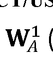 (according to, e.g., , as set forth in Equations 18 and 19), and is implemented using phase rotators, wherein the unitary

elements represented by phase rotator group 404 are used to operate on the received signals y; to form the sum representing the first element of i and the phase rotator group 406 are used to form the sum

representing the last element of
 Additional groups of rotators (not shown) similarly form the remaining elements of , which is the intermediate vector output of the first combiner 402. Similarly, second signal combiner 408 corresponding to uses groups of rotators 410 through 412 to form the intermediate

output vector A summation unit is then used to form the signals for processing by the RF chains. The summation unit includes adders 414, 416, and additional adders (not shown). Signal adder 414 combines the first elements of intermediate vectors to form the signal processed by the first RF chain 418,

signal adder 416 combines the last elements of x to form the signal processed by the last RF

chain 420, with further signal adders (not shown) forming the signals to be processed the additional RF chains (not shown). The signals from the RF chains are then processed by the Digital Combiner, which implements WD.
[0162] Note that, in some embodiments, non-unique solutions for may exist.

Flowever, via a relatively simple mathematical manipulation, one can check the validity of presented solutions in Equations 25 and 26. Some example simulation results for the example technique utilizing the above hybrid matrices will be illustrated later.
OVERALL EXAMPLE PROCEDURE
[0163] According to some embodiments, an example implementation of the overall procedure for a receiver hybrid beamformer, as illustrated by various analysis above, may be summarized as follows:
1. Estimate a receive MIMO channel.
Note that numerous techniques may be used to obtain the MIMO channel matrix, including those described above for multi-user and single-user MIMO.
2. Compute a desired fully-digital combiner as follows:

Depending on whether the system is single user or multi-user: i = (su, mu}
3. Decompose the fully-digital combiner into a product of two matrices, representing analog and digital combiners, where the analog combiner requires only Ns RF chains. As such, the dimensions of analog and digital combiners are NR x Ns and Ns x Ns , respectively.
 3.1 In one example solution, analog combiners are represented by constituent matrices which may be calculated by using Equation 26 such that:


Thus, each element of the combiner matrix may be represented as the sum of two unitary magnitude elements. In this way, each unitary element may be implemented via a phase rotation hardware device. The respective phase rotations are calculated such that the sum of the two unitary values has the desired phase, and wherein the desired magnitude is obtained according to the sum of the two unitary values in combination with a scaling factor within the digital combiner WD. The phase rotations may be determined based in part on the inverse cosine function operating on the normalized analog precoder magnitude, wherein the normalization factor is 2c. Specifically, the phase rotator angles are set by combining the original angles of the elements of the full digital combiner, with an offset by advancing
obtain the elements of In embodiments where the digital combiner is an arbitrary invertible matrix, the

remaining analog combiner matrix given by

may still be normalized to ensure the elements may obtained from the sum of two unitary elements. The normalization factor may then be further incorporated into the digital combiner matrix WD.
3.2 Subsequently, the digital combiner of the hybrid beamformer may be determined as follows:


4. Configure the receive hybrid combiner as:

In some embodiments, this is implemented by configuring the settings of the respective phase rotators according to the elements of In some embodiments, this comprises setting the phase

rotation values of the phase rotators 404 through 406, and 410 through 412 according to Equations 18, 19.
[0164] With reference to FIG. 22, a method 2200 will be described. In 2202, a desired fully-digital combiner matrix is obtained. The desired combiner matrix may be provided to the system according to know techniques. In some embodiments, the system may obtain an estimate of a receive MIMO channel, and calculate the desired fully-digital combiner matrix based on the estimate. At 2204, the method decomposes! the fully-digital combiner matrix into an analog combiner matrix and a digital combiner matrix.
The digital combiner matrix may be an arbitrary invertible matrix. In some embodiments, the digital combiner matrix may be an identity matrix scaled by the magnitude of the largest element of the fully-digital
combiner matrix. The analog combiner matrix may be normalized according to the largest element of the fully-digital combiner matrix. At 2206, the analog combiner matrix is decomposed into two constituent matrices, such that each element of the constituent matrices has unit magnitude. At 2208, the system configures phase rotators in a beamformer having two parallel analog combiners according to elements of the two constituent matrices. A processor may convey the settings to the rotators using known
configuration and control circuits. At 2210, received signals are processed using the beamformer and a plurality of radio frequency (RF) chains. In 2212, outputs of the RF chains are processed using the digital combiner matrix.
[0165] In some embodiments described herein, methods may comprise obtaining a multiple input multiple output (MIMO) signal combiner matrix, appropriate for use in either a Single Use (SU) or Multi User (MU) signaling scenario, and decomposing the MIMO signal combiner matrix into a first and a second constituent matrix, the combiner matrix being a scaled sum of the first and second constituent matrices.
The full digital combiner is advantageously decomposed into first and second constituent matrices such that each element of both of the matrices has a unitary magnitude such that it may be implemented via a simple phase rotation. In this way each constituent matrix may be implemented using hardware designed to simply provide a phase rotation to each transmit and/or received signal. In SU embodiments, the precoder and signal combiner matrices may be calculated using singular value decomposition. In MU embodiments, the MU MIMO matrix may be obtained using either a zero-forcing algorithm or a minimum mean squared error algorithm. Other well-known prior art techniques may be used to calculate or obtain the desired full digital precoder/combiner matrices, and may involve obtaining the MIMO matrix from a channel estimation procedure.
[0166] In some embodiments, a method of claim may include processing a set of receive-antenna signals using the first constituent matrix to obtain a first intermediate received signal vector; processing the set of receive-antenna signals using the second constituent matrix to obtain a second intermediate received signal vector; and, forming a set of received signals by adding corresponding elements of the first and second intermediate signal vectors, wherein the constituent matrices contain unit-magnitude (unitary) elements, that when respective elements are added together, they have the desired angle of a fully-digital beamformer, and have magnitude that is a scaled proportional to a maximum value of the fully-digital beamformer. The method may utilize first and second constituent matrices formed by offsetting the angles of MIMO signal combiner matrix.
[0167] In further embodiments, the method may include decomposing a fully-digital combiner into a product of two matrices, representing analog and digital combiners, where the analog combiner requires only Ns RF chains. The dimensions of analog and digital combiners are, in some embodiments, NR x Ns
and Ns x Ns , respectively. The fully-digital combiner WFD may be formed in accordance with WFD =
 is the analog combiner and WD the digital combiner. The analog combiner may be further decomposed into constituent beamforming matrices

Furthermore, the digital combiner of the hybrid beamformer may be represented as WD
 =cINs where Thus, the method may include processing signals with a receive hybrid combiner


[0168] Other embodiments may include an apparatus comprising a processor configured to obtain a multiple input multiple output (MIMO) signal combiner matrix and responsively generate a first and a second constituent matrices, wherein the combiner matrix is a scaled sum of the first and second constituent matrices. The apparatus may also be further configured to calculate a precoding matrix as described herein. The apparatus may further comprise: a first analog beamformer configured to process a set of receive-antenna signals using the first constituent matrix to obtain a first intermediate received signal vector; a second analog beamformer configured to process the set of receive-antenna signals using the second constituent matrix to obtain a second intermediate received signal vector; and, a summation unit configured to form a set of received signals by adding corresponding elements of the first and second intermediate signal vectors. The apparatus may further comprise a digital beamformer in the form of a scaling unit configured to apply a scaling factor to the sum of the corresponding elements of the first and second intermediate signal vectors.
SIMULATION RESULTS
[0169] Example simulation results are presented below for both SU (single user) and MU (multi-user) cases. For all of the simulations, a number of receive antennas at a BS is set to NR = 64.
[0170] FIG. 5 graphically illustrates an example of a bit error rate (BER) versus signal-to-noise ratio (SNR) for a single user (SU) scenario, in accordance with some embodiments. For an example simulation of an SU scenario, a UE is equipped with NT = 8 transmit antennas, a 4-QAM constellation is used and Ns = 8 symbols per transmission, in a mmWave channel with L = 10 paths.
[0171] More specifically, FIG. 5 depicts example BER performance versus SNR ( for

fully-digital combining, the proposed hybrid realization of fully-digital combining, as disclosed in various embodiments herein, as well as an extended realization (denoted as“hybrid design,” in FIG. 5) of reference
[9] (denoted in FIG. 5 as“Zhang et al., 2005”) (also described in references [1 1] and [14]) and a hybrid design in reference [16] (denoted in FIG. 5 as“Molu et al., 2018”).
[0172] As illustrated in FIG. 5, while the proposed hybrid design of the present disclosure essentially matches the performance of the fully-digital beamforming using only 8 RF chains, the realization technique
described in references [9], [1 1], and [14] requires twice as many RF chains, i.e., 16 RF chains. Further, the example simulation results show more than a 6 dB improvement over the hybrid design of reference [16] (Molu et al.) that uses the same number of RF chains as the hybrid realization disclosed herein.
[0173] FIG. 6 graphically illustrates an example of a bit error rate (BER) versus signal-to-noise ratio (SNR) for a multi-user (MU) scenario, in accordance with some embodiments. For an example simulation of a MU scenario, a 16-QAM constellation and an independent multipath channel model (see reference [17]) is used.
[0174] The example simulation shown in FIG. 6 compared BER performance versus SNR for a fully-digital combining, the proposed hybrid realization of fully-digital combining, as disclosed in various embodiments herein, the hybrid design realization in Zhang et al., 2005 (reference [9]) (also described in references [1 1] and [14]), and a hybrid design in reference [17] (denoted in FIG. 6 as“Li et al., 2016”).
[0175] In the example of FIG. 6, K = 8 single antenna users, and independent mmWave channels with a number of paths Lk = 15 are used. As illustrated in FIG. 6, the proposed hybrid design of the present disclosure essentially achieves the same performance as that of the fully-digital combining and outperforms the hybrid design of Li et al. (reference [17]) by more than 2 dB.
[0176] According to some embodiments, various methods and systems disclosed herein provide a hybrid analog/digital beamformer structure for massive-MIMO communication systems that may provide a substantially comparable performance (e.g., a matching performance) to the performance of, for example, any given fully-digital combiner. In some embodiments, after analyzing a minimum required number of RF chains for this purpose, a specific example decomposition technique, in accordance with some embodiments, has been presented for use with, e.g., any given matrix in a complex field, for realizing the fully-digital combiner by hybrid analog-digital beamforming. Specifically, in some embodiments, the disclosed hybrid design may achieve the performance of, e.g., optimal fully-digital combining for SU and MU scenarios. Further, the presented example simulation results illustrated some advantages (e.g., a superior performance in terms of BER (vs. SNR)) of the technique disclosed herein in accordance with some embodiments over, e.g., some recent prior hybrid designs.
SECOND EXAMPLE SYSTEM MODEL
[0177] A second example system model, in accordance with some embodiments, will be now described. The system may take the form of a generic massive-MIMO system in which a transmitter and a receiver are equipped with NT and NR antennas, respectively, as well as MT and MR RF chains, respectively. In the context of HSP, due to practical constraints for instance, it is assumed that MT « NT and MR « NR.
Conventional Hybrid Beamforming
[0178] FIG. 7 illustrates a conventional HSP architecture for a single user massive-MIMO System. Further, FIG. 7 depicts a point-to-point massive-MIMO system with conventional hybrid beamforming implemented at both ends. A transmitted signal may be formulated as follows:
 Eq. 27 where s = [s1, s2, . . . , sK]T is the symbol vector such that E{ssH} = lK with zero-mean random information symbols sk’ s taken from a discrete constellation A (such as M-QAM or M-PSK). Moreover, p is the average transmit power. Matrices
 are the digital and analog precoders, respectively, where U = {z Î C: |z| = 1}, and for normalization purposes, it is further assumed that ||PAPD ||2 F = 1. In some embodiments, the transmit beamformer matrix PA may be implemented using the decomposition technique described above, where each element of the precoder matrix may be represented as the sum of two unitary magnitudes (each obtained via a phase rotation hardware element), where the respective phase rotations are calculated such that the sum of the two unitary values has the desired phase, and wherein the desired magnitude is obtained according to the sum of the two unitary values in combination with a scaling factor within the digital precoder PD. The phase rotations may be determined using the inverse cosine function operating on the normalized analog precoder magnitude.
[0179] A received signal may be then written as follows:
y = Hx + n, Eq. 28 where is the MIMO flat fading channel matrix such that


is an additive white Gaussian noise (AWGN) vector. The decoded symbols after hybrid

processing may be expressed as follows: ŝ = DDDAy Eq. 29 where are the digital and analog combiners, respectively.

Generalized HSP System
[0180] Some embodiments disclosed herein provide for a more general formulation for HSP that extends a cascaded structure of analog and digital linear transformations presented earlier. As will be seen, such formulation may simplify, e.g., even conventional linear MIMO precoding/combining techniques.
[0181] FIG. 8 illustrates an example of a generalized HSP-based massive-MIMO transmitter, in accordance with some embodiments. FIG. 9 illustrates an example of a generalized HSP-based massive- MIMO receiver, in accordance with some embodiments.
[0182] In the generalized FISP-based massive-MIMO transmitter, as shown in FIG.8, the symbol vector s is first applied as input to the digital signal processor, whose output is a baseband signal vector expressed as:

where
 is the corresponding mapping from Then, MT parallel RF chains

convert the baseband signal vector into a bandpass modulated RF signal vector xrf
 T. The latter is

next input to an ASP network whose output is the transmit signal vector, which may be expressed as follows: Eq. 31

is the corresponding mapping.

[0183] The received RF signal y resulting from the noisy MIMO transmission is first applied as input to the ASP network and may be expressed as follows: Eq. 32

where
 The RF signal vector
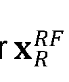

chains. Finally, x is processed in a digital domain to obtain the decoded symbols given by:

Eq. 33

where T

[0184] While in the above description, only a power constraint is imposed on the baseband mappings FR and FT, in some embodiments, the RF mappings gR and GT are implemented by RF analog components which, for example, constrain these transformations as discussed in the following section(s).
Analog Signal Processing Network
[0185] In this section, utilizing the potential of an analog signal processing domain, embodiments directed to developing a mathematical formulation for the ASP network represented, e.g., by the RF mappings GT and GR (see the discussion above) are described. Specifically, instead of focusing on conventional analog beamformer structure used, for instance, in other techniques (see, e.g., references [30]— [38]), embodiments disclosed herein focus on an arbitrarily connected network of, for example, phase shifters, power dividers and power combiners. In the description herein, signal-flow graph concepts are used which provide valuable insights for analysis of linear networks (see, e.g., references [49] and [50]).
[0186] First, individual RF components included in ASP networks are introduced. The input-output (I/O) relationship of a phase shifter is given by b = ejqa , where a, Î C are the input and output, respectively,
and Q e [0,2p] controls the phase difference between them. A passive power combiner and power divider are implemented by the same RF multi-port network but their port configuration is different. For instance, the ideal m-way Wilkinson power divider is an m + 1 port RF network, which can act as an equi-power divider if the input signal is applied to its port 1 and the outputs are taken from ports 2 to MD + 1 (see, e.g., reference
[51]). Conversely, such power divider acts as a combiner if the inputs are applied to port 2 to MD + 1 and the output is taken from port 1.
[0187] In some embodiments, to obtain a unified model for, e.g., any possible ASP network with M input ports and N output ports using primary modules (e.g., a phase shifter, a power divider and a power combiner), a convenient multi-port matrix representation of each component is presented. Further, some embodiments, include a permutation operation that may not require additional hardware and may be used mainly for the sake of mathematical simplification. The I/O relationship of the components are defined in terms of their input and outputs represented by a and b, respectively.
[0188] FIGs. 10A-1 OD depict matrix representations of ASP components, in accordance with some embodiments. More specifically, FIG. 10A illustrates an example matrix representation corresponding to a single phase shifter, in accordance with some embodiments. As illustrated in FIG. 10A, for vector a, b e Ch, the corresponding h x h matrix only changes the phase of the yth element of the RF input signal a, which can be expressed as follows:

[0189] FIG. 10B illustrates an example matrix representation corresponding to a single power divider, in accordance with some embodiments. For input vector a Î Ch' and output vector b Î Ch, the
corresponding h x h' matrix divides the yth element of the input RF signal into m equi-power signals and the remaining RF branches are not altered, and hence, h' = h - m + 1. As illustrated in FIG. 10B, this operation may be described by the following block diagonal matrix:

where 1m is an all one column vector of size m.
[0190] FIG. 10C illustrates an example matrix representation corresponding to a single power combiner, in accordance with some embodiments. This transformation may be represented by a transpose of the single power divider
 h ). Consequently, for input vector a Î Ch and output vector b Î Ch , the corresponding matrix combines m adjacent RF signals into the gth output signal and the rest of the RF branches are not altered. As shown in FIG. 10C, the following may hold:
b = QT(g, m, h)a. Eq. 36
h ). Consequently, for input vector a Î Ch and output vector b Î Ch , the corresponding matrix combines m adjacent RF signals into the gth output signal and the rest of the RF branches are not altered. As shown in FIG. 10C, the following may hold:
b = QT(g, m, h)a. Eq. 36
[0191] FIG. 10D illustrates an example permutation matrix representation, in accordance with some embodiments. This matrix corresponds to a rearrangement of input signal a
 according to the permutation p: {1,2,
 {1,2, . . . , M) which may be expressed as follows:
b = Rpa Eq. 37 where Rp = [eU1, epM]T, and ei denotes a column vector of zeros except for its ith element which is one (see FIG. 10D).
[0192] Having introduced the matrix representation of the example RF components, a mathematical formulation that may be, for instance, applicable for any given ASP network will be described, in accordance with example embodiments. FIG. 1 1 illustrates an example of an arbitrary ASP network, in accordance with some embodiments.
[0193] In some embodiments, one may arrive at the following:
[0194] Proposition 1 A: Any given RF network, with N input and M output ports, implemented by arbitrary feed-forward connections of T RF components (e.g., phase shifters, power combiners and power dividers) may be modeled as follows:

where a are the input and output RF signals, respectively, and is a 3-tuple containing

the parameters of the ith RF component.
[0195] According to some embodiments, the proof in support of the above Proposition 1 provides as follows.
[0196] In some embodiments, the matrix representations of the RF components are introduced such that the input and output signals may be of any size and thus can include the RF branches that are not affected by the RF component(s). Consequently, the RF components may be arranged such that the input of each RF component is the output of another RF component except for the first component. Let us denote the input and output of the ith RF component as
 and bi; respectively. Consequently,
 = ai, a1 = a and b = bT. To be more precise, the following algorithm may be used to assign the index i for i = 1,2, .. . , T to each RF element (component):
[0197] For i = 1 to T:
1. Find an RF component whose input is a;
2. Assign index i to that RF component
3. Denote the output as bi
4. ai+1 = bi
[0198] Note that step 1 typically has always an answer because of how and bi are defined.
Moreover, it is possible that more than one RF component satisfies the condition in step 1. In these cases, the components are parallel, meaning, e.g., that, the signals are simultaneously entering them and any ordering of these components is acceptable. Now, for i = 1,2, . . . , T , one can write bi in terms of ai. If the ith RF component is a phase shifter, a power divider, or a power combiner, then the result is that bi = respectively. Note that, if the order

of the signals is not changed before the ith component, Rp = I. Flence, a given ASP network may be expressed as given by the Equation 38.
[0199] FIG. 12 illustrates an example of the ASP network of FIG. 11 that is reorganized, in accordance with some embodiments. Namely, the ASP network of FIG. 11 may be reorganized by applying the above Proposition 1A. Note that, in the example of FIG. 12, a permutation matrix is provided only before the 7th and lSth RF components, and for the remaining components, the permutation is an identity matrix (not shown for simplicity). Moreover, note that the indexing may not be unique and parallel components may be swapped, for instance, and the order of u2, u3 and u4 does not change the I/O relationship of the ASP network.
[0200] Further, in some embodiments, Theorem 1 A provides for five commutative properties of matrices
 which, in some embodiments, may be used to rearrange the RF components for further simplifications, as will be described.
[0201] Theorem 1 A: The following commutative properties hold for two cascaded RF components:
 Eq. 39(a) Eq. 39(a)


[0202] According to some embodiments, the proofs in support of the above Theorem 1 A provide as follows.
[0203] With respect to the properties given by Equations 39(b) and 39(e), it follows that those equations are immediate results of Equations 39(a) and 39(d), respectively. The proofs for the remaining properties given by Equations 39(a), 39(c), and 39(d) are presented below.
[0204] For the property given by Equation 39(a), one can show that for any vector x, given that
 =
=

[0205] By denoting
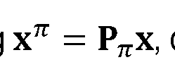 one can write:
 s one can further write:


[0206] Further, one can write: Eq. 42

and thus, one can conclude that ; therefore, there exist


[0207] For the property given by Equation 39(c), for g1 < g2 and g1 > g2 , it can be shown that / =
J' = 1 and for g1 = g2 , it will be shown that J = m1 and J' = m2.
[0208] First, considering g1 = g2, one can write:

[0209] With a matrix manipulation, one can arrive at the following:

and further, one can write:

[0210] In case of g
 1 < g2, one can accordingly write:
 [0211] Similar to Equation 44:

[0212] One can then write: ^

[0213] For y1 = g2, without a loss of generality and for illustrative purposes only, only the proof for gc = g2 = 1 and n = 1 is provided, and an extension to other values of g1,g2 and n is relatively trivial based on the following proof. Hence, one can show that: npi
 Eq. 49
[0214] The right-hand side can be written as follows:

[0215] Now, by letting
 one can write:

[0216] Forming the permutation matrix Rp with
Eq. 52

results in the following:
Eq. 53

[0217] Then, by setting gj- = j, mj· = m1 and nj = (m2 -jm1 + j, one arrives at the following:

Eq. 54

[0218] Using the above Equations 51 and 53, one can write:

[0219] The right-hand side of the above equation can be further simplified as follows:

which can be verified by invoking the mixed-product property. In this regard, the mixed-product property provides that if A, B,C and D are matrices of appropriate sizes, then

Consequently, using the above Equations 55 and 50, it has been shown that Equation 49 hold true, thus concluding the proof of the property given by Equation 39(c).
[0220] For the property given by Equation 39(d), given that:

and for g1 > g2, J is equal to one, and one can write:
 Eq. 58 and for g1 < g2, J is also equal to one, and one can write:
Eq. 59

In case of g1 = g2, J =
 m , and one can thus write:

[0221] Next, a number of RF sub-networks are introduced. As will be shown, such sub-networks provide basis for Theorem 2A, as will be described later.
[0222] FIG. 13A illustrates an example phase-shifter ASP subnetwork, in accordance with some embodiments. As shown in FIG. 13A, in some embodiments, this sub-network is an NF by NF RF module constructed by cascading J phase-shifters, where:

[0223] FIG. 13B illustrates an example power-divider ASP subnetwork, in accordance with some embodiments. As shown in FIG. 13B, in some embodiments, by cascading J power dividers, the following holds:

where
 with which is equivalent to an RF network that divides N

 signals to a total of Md signals, as illustrated in FIG. 13B.
[0224] FIG. 13C illustrates an example power-combiner ASP subnetwork, in accordance with some embodiment. As shown in FIG. 13C, in some embodiments, by cascading / power combiners, the following holds:

where

which is equivalent to an RF network that divides combines

Nc RF signals into Mc signals, as shown in FIG. 13C.
[0225] In some embodiments, validity of Equations 62, 64 and 66 may be proved as follows.
[0226] For Equation 62, to show that Ev
 is a diagonal matrix, one can use induction and the fact that for a diagonal matrix D and permutation matrix is also a diagonal matrix. For J

 =
=

1 , the statement is true, it remains to be shown that prove for J = K +, the following results:

[0227] By assuming for / = K, matrix Ev is diagonal and Rp is a permutation matrix, one can rewrite the above equation as:

[0228] One can therefore write:
Eq. 69

[0229] Using the aforementioned property of permutation matrices, it is known that
 is a diagonal matrix. Further is a permutation matrix. As a


result, thus one can write:
Eq. 70
 [0230] Since are both diagonal so is . Furthermore, since all the diagonal entries are unit

modulo complex numbers, their products are also on the unit circle and thus v =

[0231] To prove Equation 64, induction can be used. For / = 1, one can find such that:


[0232] Accordingly, there exist such that:


[0233] Using the fact that permutation matrices are orthogonal, one can write (cΐ
 ,m
,m


Eq. 73

[0234] As a result, one can thus write the following for/ = K + 1:
Eq. 74

[0235] According to the / = 1 case, there exist and such that:


thus,

[0236] Defining , and then considering ϋ the permutation matrix rearranges


the columns of Therefore, there exist permutation matrix R that rearranges the rows of to

 make a block diagonal matrix as follows:
 where
where


[0238] The above equation can be further simplified as
J

Equations 74 and 78, one has the following:
Eq. 79

which proves the property given by Equation 64.
[0239] To prove Equation 66, given / = 1, one, e.g., needs to show that Cs has the block diagonal structure of Equation 66 in According to Equation 72, one can write

Given that a product of two permutation matrices is also a

permutation matrix, the following result is obtained: To continue the proof with induction, in

some embodiments, assumption is made that for J = K , there exist
 p, h s such that =


[0241] According to the / = 1 case, there exist and such that:


[0242] Be defining a new permutation matrix Rp,3 = R^2RpiRp, the left hand-side of Equation 80 can be written as follows:

[0243] Considering permutation matrix rearranges the rows of C . Therefore, there exists


 permutation matrix R that rearranges the columns of to make a block diagonal matrix as follows:


where
 [0244] Note that it is possible that = 1 for individual i or some consecutive number indices which

result in diagonal block of identity matrices I. From Equations 82, 83, and the fact that , one can

write:
[0245] To further simplify the above equation, one can write bdiag .where:


[0246] In some embodiments, as the last step, it is taken that permutation matrices exist

such that where for some L, the following holds:


[0247] From the above equation and Equation 84, one arrives at:

[0248] Now, by defining permutation matrices as and from

Equation 80 to Equation 87, one arrives at:

which proves the statement corresponding to Equation 66.
[0249] Now, according to some embodiments, a mathematical expression for any given ASP network may be derived.
[0250] In some embodiments, according to Theorem 2A, any arbitrarily feed forward ASP network with M inputs and N outputs, implemented by phase shifters, power dividers, and power combiners may be modeled according to the following:
Eq. 89
 where a are input and output signals, respectively and


[0251] According to some embodiments, the proof in support of the above Theorem 2A provides as follows. Without loss of generality and for illustrative purposes only, let us assume there are a total of T RF components, P and R of which are combiner and dividers respectively, and the remaining Q RF components are phase shifters, namely, T = P + Q + R. According to the properties given by Equations 39(b), 39(c)
and 39(e) in Theorem 1A, Equation 38 can be rewritten as follows by commuting the combiner matrices to the left hand side, so that:
 where V = T - P. Similarly, the divider matrices can be moved to the right-hand side using the properties in Equations 39(a), 39(c) and 39(e), thus resulting in the following:
 Eq. 91 where T" = T - P - R. In Equation 91 , only the permutation and single phase-shifter matrices are in the middle of the expression. Therefore, without loss of generality and for illustrative purposes only, given that permutation and single phase-shifter matrices can be identity matrices, the following can be derived:

[0252] Now, using Equations 61 , 63, and 65 and the fact that product of permutation matrices is another permutation matrix, the following holds: Eq. 93

which follows,
Eq. 94

[0253] By defining the following:


Eq. 101

[0255] Without loss of generality, one can further have the following:
Eq. 102


[0256] By defining , one can write:

Eq. 103

[0257] Since in , by adding even number of phase-shifters which can cancel each other


the sum remains the same, and the result may beLK =


Eq. 104
 hence,
Eq. 105

[0258] Further, let us assume L is even and from Lemma 1 B (to be described later) one can write: Eq. 106
 [0259] Thus, the following expression results:
Eq. 107

[0260] Lemma 1 B mentioned above holds that any complex number z where for an even

number L can be written as: , where might be non-unique.


[0261] According to some embodiments, the proof for L = 2 is presented , for example in reference
[32], thus, for Consequently, for L z can be written as z = L'z'


, where 0 £ |z'| £ 2. Therefore, similarly z can be written as

[0262] From the above Theorem 2A, it is apparent that that the example network shown in FIG. 11 is equivalent to the one in FIG. 15. Namely, FIG. 15 illustrates an example of a minimal equivalent of the ASP network of FIG. 1 1 , in accordance with some embodiments.
[0263] Now, some embodiments of the present disclosure look to whether any matrix in a convex set UNxM can be realized by an ASP network.
[0264] In some embodiments, according to Theorem 3A, any given matrix A
 can be realized by an ASP network with N dividers, M combiners, and 2 NM phase-shifters, such as one shown by way of example, in FIG. 14. FIG. 14 illustrates an example of a proposed ASP architecture, in accordance with some embodiments.
[0265] In FIG. 14, for a given A, the output of the ASP network for the input vector a may be written as in Equation 106. By invoking Lemma 1A, for any Equation 106 can be written as Equation 105.

Moreover, the smallest possible L is equal to two according to Lemma 1A. Thus, 2 M phase-shifters are required for each element of b and consequently, the minimum of 2 MN phase-shifters are needed. FIG. 14 illustrates the ASP network architecture corresponding to Equation 105 which proves the Theorem 3A.
[0266] The remainder of the present disclosure considers the ASP network as shown in FIG. 15 , GT
 (see Equation 31 ) and gR (see Equation 32) are substituted by: 108

[0267] One significant result of Theorem 3A, is that there exist an ASP structure which is not bound to the unit modulus constraint. Thus, the non-convexity constraint can be lifted from the design optimization problems.
TRANSMITTER AND RECEIVER DESIGN WITH HSP
[0268] Considering Equations 30, 31 , and 108, the transmitted signal of the generalized HSP can be written as follows:
Eq. 109

[0269] In the art of hybrid beamforming, FT is usually a linear transformation, i.e.,

where is the precoding matrix.

[0270] Here, the properties, structure and implementation of FT are first explored and then the description discusses a design of FT and AT at an HSP-based transmitter.
HSP Design at the Transmitter
[0271] Various principles disclosed herein may apply to different communication techniques. Let us assume that Tt{ s) generates a desired transmitted signal for the given vector symbol s. Note that this function can represent all communication modes and techniques at the transmitter side. By way of example, the optimal eigen-mode precoding is obtained by solving the following problem:
[0272]

[0273] The solution is given by:
P = VYs Eq. 1 11 where the diagonal weight matrix W is calculated via water filling (see, e.g., reference [52]) and V is obtained from a singular value decomposition of channel matrix, e.g.,
 Eq. 1 12
[0274] Consequently, the transmitter generation function can be defined as:
Tt(s) = VYs Eq. 1 13
[0275] In some embodiments, nonlinear beamforming, channel estimation, space-time coding and many other techniques can also be modeled by Tt{ s). From Equation 109, in some embodiments, the
HSP serves its purpose when for a given Tt{ s), there exist A and FT{. ) such that:
ATFT (.S) = 7Y(s) Eq. 1 14 holds for all symbol vectors s. Hence, since Tt( s) is given, TT( s) can be found as:
 Eq. 1 15
[0276] Despite apparent simplicity of the above solution, it has a rather significant result, such as for example, the mapping TT(. ) itself may not be found because the value of Tt( s) is available and AT is
either given or must be designed alongside FT(. ). Given the flexibility of a digital domain, in some embodiments, the system may only need to calculate the desired output of FT(. ) rather than the function itself.
[0277] From Equations 30 and 115, one can rewrite Equation 114 as follows: Eq. 1 16

which means, in general, that the HSP objective is: designing AT and such that Equation 116 is satisfied

fora given Tt(s) and for all possible vectors s.
[0278] This objective, however, is not limiting and other variations can be, in some embodiments, derived according to the conditions and constraints of the system.
[0279] In practice, depending on the system constraints, one may wish to design AT, and some

additional parameter vector p with either of the following optimization formulations:
Eq. 1 17

and:
Eq. 1 18

where /(. ) is a cost function of some sort relevant to the objectives of the system. Note that, the power constraints may not be necessary as normally those are taken into account when designing Tt{ s). One

possible choice is = 1, thus, AT is designed such that for some set cols(AT) =


Tt( s), "s Î S , exist, where cols(AT) denotes the column space of AT. Consequently, the baseband signal is obtained form
 In what follows, two different cost functions are presented for designing precoding with HSP.
Unconstrained FD Precoding
[0280] Here, a goal is to realize any given FD precoder. As an example, optimal eigen-mode precoding is explored, although any other precoding matrix can be obtained in the same fashion. From Equations 1 13 and 1 16, both AT and must be designed such that:


[0281] The problem for MT = K has the following solution:
Eq. 120
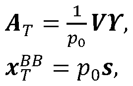
where Note that, in this particular example embodiment, no constraint is imposed
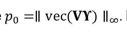
upon the system and AT is updated according to the channel coherence time, Tc. Since s changes after every symbol duration
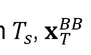 is also updated Ts seconds.
Minimum Number of RF Chains
[0282] In some embodiments, if a constraint on the update rate of the analog components does not exist, the number of RF chains may be reduced by solving the following problem:
Eq. 121
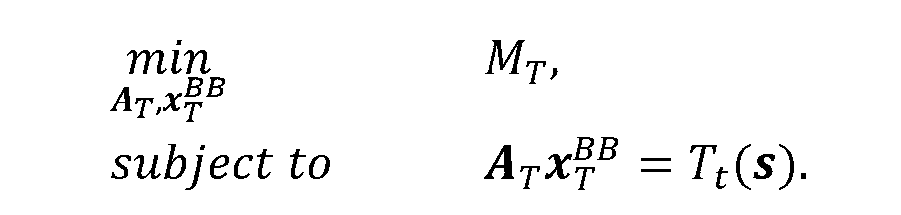
[0283] This problem is shown to have a non-unique solution for MT = 1 where Tt( s) = VWs (see, e.g., reference [39]) but essentially the same solution is valid for any other transmit function Tt{ s). Note that, in this case, the ASP must be updated after every symbol duration Ts.
HSP Design at the Receiver
[0284] By substituting Equations 32 and 108 in Equation 33, the estimated signal at the receiver is expressed as follows:
Eq. 122
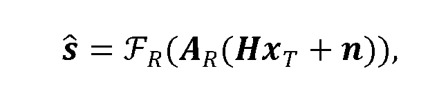
[0285] As shown above, the same remedy that was used already for FT(. ) would not be applied here because the output of FR (. ) is unknown, and thus the mapping itself is what is desired. However, similar to the discussions in earlier sections, it may be assumed that the function Tr (y) is given. Function Tr (y) can be interpreted as the FD receiver in a more general sense. Ideally, one wants to find FR and AR such that:
FR(ARy) = Tr(y). Eq. 123
[0286] Nevertheless, for MIMO and especially massive-MIMO systems where beamforming and multiplexing are typically the utilized techniques, the receiver is almost always a linear operation which is why multi-stream beamforming at the receiver is usually called combining. Given Tr(y) = Zy , where Z Î
 is the FD combiner matrix. Moreover, if the computational limitation of the system allows, in some
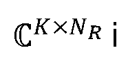
embodiments, Tr(y) can be extended to optimal detectors such as ML which improves the overall performance. However, here consideration is given to the linear functions similar to the HSP described in the art and extension to other functions are typically straight forward by using Equation 123. Thus, similar
to the transmitter side, the two following general optimization forms to obtain and

the parameter vector p are obtained:
 Eq. 124 subject to Constraints,
and
Eq. 125

[0287] Hence, according to some embodiments, a matrix factorization problem, which can be solved under various conditions, has been provided. In the following discussion. FD combining is presented as an example.
Unconstrained FD Combining
[0288] In some embodiments, the, e.g., optimal FD combiner may be obtained by solving the following problem:
Eq. 126

where from Equation 112, it follows that:
ZH = Ua. Eq. 127
[0289] where U = [Ua, Ub
 ] and Ua contains the first K columns of U. Thus, in some embodiments, both AR and W are designed such that:
WAR = Z. Eq. 128
[0290] Note that if MT = K, for any FD combiner this problem has the following solution:

Eq. 129

where

[0291] Thus, some embodiments may include an apparatus comprising: a radio frequency (RF) analog signal processing (ASP) network, having N input and M output ports, comprising feed-forward connections of T RF components, the RF components selected from the group comprising phase-shifters, power combiners and power dividers. The ASP of the apparatus may be modeled as
 where a are input and output signals, respectively and


[0292] The ASP apparatus may represent a given matrix
 comprising N dividers, M combiners, and 2NM phase-shifters. The ASP may have a plurality of signal splitters, each signal splitter configured to process a signal received from an antenna element and to generate a set of power-divided output signals; a plurality of sets of configurable phase shifters, each set of configurable phase shifters operating on a respective set of power-divided output signals to generate sets of phase-shifted power- divided output signals; a plurality of signal combiners, each signal combiner receiving a plurality of phase- shifted power-divided output signals and providing a combined output signal. The ASP may include signal combiners receiving two phase-shifted power-divided output signals from each set of configurable phase shifters. Embodiments of a method may comprise: processing a plurality of signals using a radio frequency (RF) analog signal processing (ASP) network, having N input and M output ports, comprising feed-forward connections of T RF components, the RF components selected from the group comprising phase-shifters, power combiners and power dividers. Another method may comprise configuring an ASP comprising N dividers, M combiners, and 2NM phase-shifters to implement a given matrix

[0293] A further method may comprise: processing a signal received from an antenna element using a plurality of signal splitters, each signal splitter configured to generate a set of power-divided output signals; operating on a respective set of power-divided output signals using a plurality of sets of configurable phase shifters, each set of configurable phase shifters configured to generate sets of phase-shifted power-divided output signals; and, receiving a plurality of phase-shifted power-divided output signals at a plurality of signal combiners, each signal combiner providing a combined output signal.
SIMULATION RESULTS
[0294] Example simulation results are presented below results for different scenarios and reception modes, and compare a FD system with our hybrid architecture embodiments disclosed herein and other recent hybrid designs. The following channel models have been used for all the simulations:
Eq. 130

where Nc is the number of clusters and is set to 5, and the number of rays in each clusters is set to Nray = 10. Similar to references [31] and [42], it is assumed that and transmit/receive antenna

responses are denoted by respectively, where:

Eq. 131
 for linear arrays of size N.
[0295] The angles of arrival and departure are are independently and uniformly distributed in
for linear arrays of size N.
[0295] The angles of arrival and departure are are independently and uniformly distributed in

[0,2p] The angular spread is 10 degrees within each cluster. Further, the simulations assume that the channel estimation and system synchronization are essentially perfect. The numbers of RF chains and transmitted symbols are set to MT = K = 2 , and 64-QAM modulation is used for all the simulations. Simulation results for optimal FD beamforming, proposed hybrid precoder and combiner realization of FD in accordance with various embodiments described herein, as well as hybrid designs described in references
[31] (hereinafter“Sohrabi et al.”), [42] (hereinafter“Lin et al.”), and [53] (hereinafter“Nguyen et al.”) are presented.
Bit Error Rate (BER) Performance
[0296] BER performance versus for three different setups are depicted in

references 16 to 18. FIG. 16 graphically illustrates an example of a bit error rate (BER) versus signal-to- noise ratio (SNR) for different methods for 64x64 massive-MIMO system, in accordance with some embodiments. FIG. 17 graphically illustrates an example of a bit error rate (BER) versus signal-to-noise ratio (SNR) for different methods with NT = 64 massive_MIMO base station (BS) and NR = 2 at a receiver, in accordance with some embodiments. Further, FIG. 18 graphically illustrates an example of a bit error rate (BER) versus signal-to-noise ratio (SNR) for different methods with NTR = 2 massive_MIMO base station (BS) and NT = 2 at a transmitter, in accordance with some embodiments.
[0297] FIG. 16 depicts simulation results for 64 x 64 massive-MIMO system with MT = 2 RF chains. Downlink BER of a massive-MIMO BS with NT = 64 antennas transmitting to a single UE with NT = 2 is illustrated in the references, and the uplink transmission of the same system is depicted in FIG. 18. It can be seen that in all the simulated scenarios, the proposed hybrid realization in accordance with various embodiments disclosed herein essentially matches the performance of the FD systems while outperforming the existing hybrid designs. The FD systems require MT = 64 and RF chains whereas the proposed design may achieve the same performance with only MT = 2 RF chains. Consequently, the proposed design outperforms the existing hybrid designs (such as those, e.g., of Lin et al., Nguyen et al., and Sohrabi et al.) with the same number of RF chains.
Spectral Efficiency
[0298] Spectral efficiency of optimal FD beamforming, proposed hybrid realization of FD as well as hybrid designs in Lin et al., Nguyen et al., and Sohrabi et al. for 64 x 64 massive-MIMO system is depicted in 19. Furthermore, single user uplink and downlink connection of 16 x 64 and 64 x 4 are presented in FIG. 20 and 21 respectively. As expected, the proposed realization achieves the same rate as FD systems and has higher rate than existing designs.
[0299] FIG. 19 illustrates spectral efficiency versus signal-to-noise ratio (SNR) for different methods in a 64x64 massive-MIMO system, in accordance with some embodiments. FIG. 20 illustrates spectral efficiency versus signal-to-noise ratio (SNR) for different methods in a 16x64 massive-MIMO, in accordance with some embodiments. FIG. 21 illustrates spectral efficiency versus signal-to-noise ratio (SNR) for different methods in a 64x4 massive-MIMO system, in accordance with some embodiments.
[0300] Spectral efficiency of , e.g., optimal FD beamforming, proposed hybrid realization of FD as well as hybrid designs in Lin et al., Nguyen et al., and Sohrabi et al. for 64 x 64 massive-MIMO system is depicted in FIG. 19. Furthermore, a single user uplink and downlink connection of 16 x 64 and 64 x 4 systems are presented in FIGs. 20 and 21 , respectively. As depicted, the proposed realization achieves essentially the same rate as FD systems and has a higher rate than existing designs (such as those, e.g., of Lin et al., Nguyen et al., and Sohrabi et al.).
[0301] Note that various hardware elements of one or more of the described embodiments are referred to as“modules” that carry out (i.e., perform, execute, and the like) various functions that are described herein in connection with the respective modules. As used herein, a module includes hardware (e.g., one or more processors, one or more microprocessors, one or more microcontrollers, one or more microchips, one or more application-specific integrated circuits (ASICs), one or more field programmable gate arrays (FPGAs), one or more memory devices) deemed suitable by those of skill in the relevant art for a given implementation. Each described module may also include instructions executable for carrying out the one or more functions described as being carried out by the respective module, and it is noted that those instructions could take the form of or include hardware (i.e., hardwired) instructions, firmware instructions, software instructions, and/or the like, and may be stored in any suitable non-transitory computer-readable medium or media, such as commonly referred to as RAM, ROM, etc.
[0302] Although features and elements are described above in particular combinations, one of ordinary skill in the art will appreciate that each feature or element can be used alone or in any combination with the other features and elements. In addition, the methods described herein may be implemented in a computer program, software, or firmware incorporated in a computer-readable medium for execution by a computer or processor. Examples of computer-readable storage media include, but are not limited to, a read only memory (ROM), a random access memory (RAM), a register, cache memory, semiconductor memory devices, magnetic media such as internal hard disks and removable disks, magneto-optical media, and optical media such as CD-ROM disks, and digital versatile disks (DVDs). A processor in association with software may be used to implement a radio frequency transceiver for use in a WTRU, UE, terminal, base station, RNC, or any host computer.
REFERENCES
The following references describe background information with well-known MIMO signal processing details, and re incorporated by reference herein.
[1] E. Telatar,“Capacity of multi-antenna gaussian channels,” European Transactions on
Telecommunications, vol. 10, no. 6, pp. 585-595, 1999.
[2] S. A. Busari, K. M. S. Huq, S. Mumtaz, L. Dai, and J. Rodriguez,“Millimeter-Wave Massive MIMO Communication for Future Wireless Systems: A Survey,” IEEE Communications Surveys Tutorials, vol. PP, no. 99, pp. 1-1, 2017.
[3] R. C. Daniels and R. W. Heath,“60 ghz wireless communications: Emerging requirements and design recommendations,” IEEE Trans. Veh. Technol., vol. 2, no. 3, pp. 41-50, Sept. 2007.
[4] E. G. Larsson, O. Edfors, F. Tufvesson, and T. L. Marzetta,“Massive mimo for next generation wireless systems,” IEEE Commun. Mag., vol. 52, no. 2, pp. 186-195, Feb. 2014.
[5] F. Rusek, D. Persson, B. K. Lau, E. G. Larsson, T. L. Marzetta, 0. Edfors, and F. Tufvesson, “Scaling up mimo: Opportunities and challenges with very large arrays,” IEEE Signal Processing Mag., vol. 30, no. 1, pp. 40-60, Jan. 2013.
[6] E. Torkildson, U. Madhow, and M. Rodwell,“Indoor millimeter wave mimo: Feasibility and performance,” IEEE Trans. Wireless Commun., vol. 10, no. 12, pp. 4150-4160, Dec. 2011.
[7] S. Hur, T. Kim, D. J. Love, J. V. Krogmeier, T. A. Thomas, and A. Ghosh,“Millimeter wave beamforming for wireless backhaul and access in small cell networks,” IEEE Trans. Commun., vol. 61, no. 10, pp. 4391-4403, Oct. 2013.
[8] A. Alkhateeb, J. Mo, N. Gonzalez-Prelcic, and R. W. Heath,“MIMO Precoding and Combining Solutions for Millimeter-Wave Systems,” IEEE Commun. Mag., vol. 52, no. 12, pp. 122-131, Dec. 2014.
[9] X. Zhang, A. F. Molisch, and S.-Y. Kung,“Variable-phase-shift-based RF-baseband codesign for MIMO antenna selection,” IEEE Trans. Signal Processing, vol. 53, no. 11, pp. 4091-4103, Nov. 2005.
[10] 0. E. Ayach, S. Rajagopal, S. Abu-Surra, Z. Pi, and R. W. Heath,“Spatially sparse precoding in millimeter wave MIMO systems,” IEEE Trans. Wireless Commun., vol. 13, no. 3, pp. 1499-1513, Mar.
2014.
[11] F. Sohrabi and W. Yu,“Hybrid digital and analog beamforming design for large-scale antenna arrays,” IEEE J. Sel. Topics Signal Process., vol. 10, no. 3, pp. 501-513, Apr. 2016.
[12] F. Khalid,“Hybrid beamforming for millimeter wave massive multiuser mimo systems using regularized channel diagonalization,” IEEE Commun. Lett., pp. 1-1, 2018.
[13] T. Lin, J. Cong, Y. Zhu, J. Zhang, and K. B. Letaief,“Hybrid beamforming for millimeter wave systems using the mmse criterion,” IEEE Trans. Commun., pp. 1-1, 2019.
[14] T. E. Bogale, L. B. Le, A. Haghighat, and L. Vandendorpe,“On the Number of RF Chains and Phase Shifters, and Scheduling Design With Hybrid Analog Digital Beamforming,” IEEE Trans. Wireless Commun., vol. 15, no. 5, pp. 3311-3326, May 2016.
[15] A. Morsali, A. Haghighat, and B. Champagne,“Realizing Fully Digital Precoders in Hybrid A/D Architecture With Minimum Number of RF Chains,” IEEE Commun. Lett., vol. 21, no. 10, pp. 2310-2313, Oct. 2017.
[16] M. M. Molu, P. Xiao, M. Khalily, K. Cumanan, L. Zhang, and R. Tafazolli,“Low-complexity and robust hybrid beamforming design for multi-antenna communication systems,” IEEE Trans. Wireless Commun., vol. 17, no. 3, pp. 1445-1459, Mar. 2018.
[17] J. Li, L. Xiao, X. Xu, and S. Zhou,“Robust and low complexity hybrid beamforming for uplink multiuser mmwave MIMO systems,” IEEE Commun. Lett., vol. 20, no. 6, pp. 1140-1143, June 2016.
[18]. R. C. Daniels and R. W. Heath,“60 GHz wireless communications: Emerging requirements and design recommendations,” vol. 2, no. 3, pp. 41-50, 2007.
[19]. F. Rusek, D. Persson, B. K. Lau, E. G. Larsson, T. L. Marzetta, O. Edfors, and F. Tufvesson, “Scaling up MIMO: Opportunities and challenges with very large arrays,” vol. 30, no. 1, pp. 40-60, 2013.
[20]. E. G. Larsson, 0. Edfors, F. Tufvesson, and T. L. Marzetta,“Massive MIMO for next generation wireless systems,” vol. 52, no. 2, pp. 186-195, 2014.
[21] I. F. Akyildiz, C. Han, and S. Nie,“Combating the distance problem in the Millimeter wave and
Terahertz frequency bands,” vol. 56, no. 6, pp. 102-108, 2018.
[22] E. Bjornson, L. Sanguinetti, H. Wymeersch, J. Hoydis, and T. Marzetta,“Massive MIMO is a reality— What is next?” Digital Signal Processing, Jun. 2019.
[23]. S. A. Busari, K. M. S. Huq, S. Mumtaz, J. Rodriguez, Y. Fang, D. C. Sicker, S. Al-Rubaye, and A. Tsourdos,“Generalized hybrid beamforming for vehicular connectivity using THz massive MIMO,” pp. 1-1, 2019.
[24] S. A. Busari, K. M. S. Huq, S. Mumtaz, L. Dai, and J. Rodriguez,“Millimeter-wave massive MIMO communication for future wireless systems: A survey,” IEEE Communications Surveys Tutorials, vol. PP, no. 99, pp. 1-1, 2017.
[25]. X. Zhang, A. F. Molisch, and S.-Y. Kung,“Variable-phase-shift-based RF-baseband codesign for
MIMO antenna selection,” vol. 53, no. 11, pp. 4091-4103, 2005.
[26]. A. Alkhateeb, J. Mo, N. Gonzalez-Prelcic, and R. W. Heath,“MIMO precoding and combining solutions for millimeter-wave systems,” vol. 52, no. 12, pp. 122-131, 2014.
[27], A. Morsali, S. S. Hosseini, B. Champagne, and X. Chang,“Design criteria for omnidirectional
STBC in massive -MIMOSystems,” pp. 1-1, 2019.
[28]. F. Koroupi, A. Morsali, V. Niktab, M. Shahabinejad, and S. Talebi,“Quasi-orthogonal space- frequency and space-time-frequency block codes with modified performance and simplified decoder,” vol.
11, no. 11, pp. 1655-1661, 2017.
[29]. M. Samavat, A. Morsali, and S. Talebi,“Delay interleaved cooperative relay networks,” vol. 18, no.
12, pp. 2137-2140, 2014.
[30]. O. E. Ayach, S. Rajagopal, S. Abu-Surra, Z. Pi, and R. W. Heath,“Spatially sparse precoding in millimeter wave MIMO systems,” vol. 13, no. 3, pp. 1499-1513, 2014.
[31]. F. Sohrabi and W. Yu,“Hybrid digital and analog beamforming design for large-scale antenna arrays,” vol. 10, no. 3, pp. 501-513, 2016.
[32], T. E. Bogale, L. B. Le, A. Haghighat, and L. Vandendorpe,“On the number of rf chains and phase shifters, and scheduling design with hybrid analog digital beamforming,” vol. 15, no. 5, pp. 3311-3326, May 2016.
[33]. X. Yu, J. C. Shen, J. Zhang, and K. B. Letaief,“Alternating minimization algorithms for hybrid precoding in millimeter wave MIMO systems,” vol. 10, no. 3, pp. 485-500, 2016.
[34], F. Khalid,“Hybrid beamforming for millimeter wave massive multiuser mimo systems using regularized channel diagonalization,” vol. 8, no. 3, pp. 705-708, 2019.
[35]. M. M. Molu, P. Xiao, M. Khalily, K. Cumanan, L. Zhang, and R. Tafazolli,“Low-complexity and robust hybrid beamforming design for multi-antenna communication systems,” vol. 17, no. 3, pp. 1445— 1459, 2018.
[36]. J. Li, L. Xiao, X. Xu, and S. Zhou,“Robust and low complexity hybrid beamforming for uplink multiuser mmwave MIMO systems,” vol. 20, no. 6, pp. 1140-1143, 2016.
[37], C. Ho, H. Cheng, and Y. Huang,“Hybrid precoding processor for millimeter wave MIMO communications,” pp. 1-1, 2019.
[38]. R. Mai, D. H. N. Nguyen, and T. Le-Ngoc,“MMSE hybrid precoder design for millimeter-wave massive MIMO systems,” in Proc. IEEE WCNC, 2016, pp. 1-6.
[39]. A. Morsali, A. Haghighat, and B. Champagne,“Realizing fully digital precoders in hybrid A/D architecture with minimum number of rf chains,” vol. 21, no. 10, pp. 2310-2313, 2017.
[40]. A. Alkhateeb and R. W. Heath,“Frequency selective hybrid precoding for limited feedback millimeter wave systems,” vol. 64, no. 5, pp. 1801-1818, May 2016.
[41]. F. Sohrabi and W. Yu,“Hybrid analog and digital beamforming for mmWave ofdm large-scale antenna arrays,” vol. 35, no. 7, pp. 1432-1443, 2017.
[42] T. Lin, J. Cong, Y. Zhu, J. Zhang, and K. B. Letaief,“Hybrid beamforming for millimeter wave systems using the mmse criterion,” pp. 1-1, 2019.
[43]. A. Alkhateeb, O. E. Ayach, G. Leus, and R. W. Heath,“Channel estimation and hybrid precoding for millimeter wave cellular systems,” vol. 8, no. 5, pp. 831-846, 2014.
[44] K. Venugopal, A. Alkhateeb, N. G. Prelcic, and R. W. Heath,“Channel estimation for hybrid architecture-based wideband millimeter wave systems,” vol. 35, no. 9, pp. 1996-2009, 2017.
[45]. C. Tsai and A. Wu,“Structured random compressed channel sensing for millimeter-wave large- scale antenna systems,” vol. 66, no. 19, pp. 5096-5110, Oct. 2018.
[46]. Z. Zhou, J. Fang, L. Yang, H. Li, Z. Chen, and R. S. Blum,“Low-rank tensor decomposition-aided channel estimation for millimeter wave mimo-ofdm systems,” vol. 35, no. 7, pp. 1524-1538, 2017.
[47] Y. Zhang, D. Wang, J. Wang, and X. You,“Channel estimation for massive MIMO-OFDM systems by tracking the joint angle-delay subspace,” IEEE Access, vol. 4, pp. 10166-10179, 2016.
[48]. L. Pan, L. Liang, W. Xu, and X. Dong,“Framework of channel estimation for hybrid analog-and- digital processing enabled massive MIMO communications,” vol. 66, no. 9, pp. 3902-3915, 2018.
[49]. S. C. Elwood, The theory and design of linear differential equation machines. 1942.
[50]. F. Bonchi, P. Sobocinski, and F. Zanasi,“The calculus of signal flow diagrams I: Linear relations on streams,” Information and Computation, vol. 252, pp. 2-29, 2017.
[51]. D. M. Pozar, Microwave engineering. John Wiley; Sons,., 2005.
[52] E. Torkildson, U. Madhow, and M. Rodwell,“Indoor millimeter wave MIMO: Feasibility and performance,” vol. 10, no. 12, pp. 4150-4160, 2011.
[53]. D. H. N. Nguyen, L. B. Le, T. Le-Ngoc, and R. W. Heath,“Hybrid MMSE precoding and combining designs for mmWave multiuser systems,” IEEE Access, vol. 5, pp. 19167-19181, 2017.
Claims
1. A method comprising:
obtaining an estimate of a receive MIMO channel;
computing a desired fully-digital combiner matrix based on the estimate;
decomposing the fully-digital combiner matrix into an analog combiner matrix and a digital combiner matrix;
decomposing the analog combiner matrix into two constituent matrices, such that each element of the constituent matrices has unit magnitude;
configuring phase rotators in a beamformer having two parallel analog combiners according to elements of the two constituent matrices;
processing received signals using the beamformer and a plurality of radio frequency (RF) chains; and,
processing outputs of the RF chains using the digital combiner matrix.
2. The method of claim 1 wherein the desired fully-digital combiner is WFD , and is based on:
s, where

3. The method of claim 1 wherein the constituent matrices are
 , and wherein the phase rotators of the two parallel analog combiners are configured according to respectively.

4. The method of claim 1 wherein each element of the two constituent matrices has an angle based on a combination of a corresponding angle of an element of the fully-digital combiner matrix, and an offset angle.
5. The method of claim 4 wherein the offset angle is a positive angle for an element of one constituent matrix of the two constituent matrices, and the offset angle is a negative angle for an element of the other constituent matrix of the two constituent matrices.
6. The method of claim 1 , wherein the beamformer further comprises a summation circuit for combining a first and second intermediate signal vector generated by the respective analog combiner of the two parallel analog combiners.
7. The method of claim 1 wherein a phase of each element of the constituent matrices is based on an inverse cosine function operating on a normalized magnitude of the fully-digital combiner matrix.
8. The method of claim 1 wherein the digital combiner matrix is an arbitrary invertible matrix.
9. The method of claim 1 wherein the digital combiner matrix is a scaled identity matrix given by WD = clNs, where c is one half the magnitude of the largest element of the fully-digital combiner matrix, and INsis an identify matrix having dimension Ns.
10. An apparatus comprising:
a beamformer having two parallel analog combiners, each of the parallel analog combiners having a plurality of sets of phase rotation circuits configured to generate a respective plurality of outputs as a respective intermediate output vector;
a summation circuit configured to combine the respective intermediate output vectors to generate an analog beam-formed signal vector;
a processor configured to:
obtain a desired fully-digital combiner matrix, and decompose the fully-digital combiner matrix into an analog combiner matrix and a digital combiner matrix;
decompose the analog combiner matrix into two constituent matrices, such that each element of the constituent matrices has unit magnitude;
configuring the sets of phase rotators according to elements of the two constituent matrices;
a plurality of radio frequency (RF) chains, each RF chain configured to process a signal from the analog beam-formed signal vector; and,
a digital combiner circuit configured to apply the digital combiner matrix to outputs of the plurality of RF chains.
1 1. The apparatus of claim 10 wherein each element of the two constituent matrices has an angle based on a combination of a corresponding angle of an element of the fully-digital combiner matrix, and an offset angle.
12. The apparatus of claim 1 1 wherein the offset angle is a positive angle for an element of one constituent matrix of the two constituent matrices, and the offset angle is a negative angle for an element of the other constituent matrix of the two constituent matrices.
13. The apparatus of claim 10 wherein a phase of each element of the constituent matrices is based on an inverse cosine function operating on a normalized magnitude of the fully-digital combiner matrix.
14. The apparatus of claim 10 wherein the digital combiner matrix is an arbitrary invertible matrix.
15. The apparatus of claim 10 wherein the digital combiner matrix is a scaled identity matrix given by WD = clNs, where c is one half the magnitude of the largest element of the fully-digital combiner matrix, and INsis an identify matrix having dimension Ns.
Applications Claiming Priority (4)
| Application Number | Priority Date | Filing Date | Title |
|---|---|---|---|
| US201962822613P | 2019-03-22 | 2019-03-22 | |
| US62/822,613 | 2019-03-22 | ||
| US201962950789P | 2019-12-19 | 2019-12-19 | |
| US62/950,789 | 2019-12-19 |
Publications (1)
| Publication Number | Publication Date |
|---|---|
| WO2020198168A1 true WO2020198168A1 (en) | 2020-10-01 |
Family
ID=70471078
Family Applications (1)
| Application Number | Title | Priority Date | Filing Date |
|---|---|---|---|
| PCT/US2020/024318 Ceased WO2020198168A1 (en) | 2019-03-22 | 2020-03-23 | Receiver combining for hybrid analog-digital beamforming |
Country Status (1)
| Country | Link |
|---|---|
| WO (1) | WO2020198168A1 (en) |
Cited By (6)
| Publication number | Priority date | Publication date | Assignee | Title |
|---|---|---|---|---|
| CN112285746A (en) * | 2020-10-21 | 2021-01-29 | 厦门大学 | Deception detection method and device based on multipath signals |
| CN112636800A (en) * | 2020-12-16 | 2021-04-09 | 杭州电子科技大学 | Mixed precoding algorithm based on millimeter wave large-scale MIMO multi-user scene |
| CN115103029A (en) * | 2022-05-20 | 2022-09-23 | 西安邮电大学 | Low-rank tensor completion QoS prediction method and device based on truncated nuclear norm |
| CN115459820A (en) * | 2022-08-31 | 2022-12-09 | 北京瀚景锦河科技有限公司 | Low-complexity manifold optimization hybrid pre-coding method based on quasi-Newton method |
| CN116846439A (en) * | 2023-05-17 | 2023-10-03 | 深圳市大数据研究院 | Clustered beamforming method, communication sensing and computing integrated system and related devices |
| TWI851016B (en) * | 2022-02-11 | 2024-08-01 | 瑞典商賓威公司 | A method for a multi-antenna receiver arrangement, a computer program product, a multi-antenna receiver arrangement, and a wireless device |
Citations (1)
| Publication number | Priority date | Publication date | Assignee | Title |
|---|---|---|---|---|
| WO2018136581A1 (en) * | 2017-01-19 | 2018-07-26 | Idac Holdings, Inc. | Efficient implementation of hybrid beamforming |
-
2020
- 2020-03-23 WO PCT/US2020/024318 patent/WO2020198168A1/en not_active Ceased
Patent Citations (1)
| Publication number | Priority date | Publication date | Assignee | Title |
|---|---|---|---|---|
| WO2018136581A1 (en) * | 2017-01-19 | 2018-07-26 | Idac Holdings, Inc. | Efficient implementation of hybrid beamforming |
Non-Patent Citations (53)
| Title |
|---|
| A. ALKHATEEBJ. MON. GONZALEZ-PRELCICR. W. HEATH, MIMO PRECODING AND COMBINING SOLUTIONS FOR MILLIMETER-WAVE SYSTEMS, vol. 52, no. 12, 2014, pages 122 - 131 |
| A. ALKHATEEBJ. MON. GONZALEZ-PRELCICR. W. HEATH: "MIMO Precoding and Combining Solutions for Millimeter-Wave Systems", IEEE COMMUN. MAG., vol. 52, no. 12, December 2014 (2014-12-01), pages 122 - 131, XP011567668, DOI: 10.1109/MCOM.2014.6979963 |
| A. ALKHATEEBO. E. AYACHG. LEUSR. W. HEATH, CHANNEL ESTIMATION AND HYBRID PRECODING FOR MILLIMETER WAVE CELLULAR SYSTEMS, vol. 8, no. 5, 2014, pages 831 - 846 |
| A. ALKHATEEBR. W. HEATH, FREQUENCY SELECTIVE HYBRID PRECODING FOR LIMITED FEEDBACK MILLIMETER WAVE SYSTEMS, vol. 64, no. 5, May 2016 (2016-05-01), pages 1801 - 1818 |
| A. MORSALIA. HAGHIGHATB. CHAMPAGNE, REALIZING FULLY DIGITAL PRECODERS IN HYBRID A/D ARCHITECTURE WITH MINIMUM NUMBER OF RF CHAINS, vol. 21, no. 10, 2017, pages 2310 - 2313 |
| A. MORSALIA. HAGHIGHATB. CHAMPAGNE: "Realizing Fully Digital Precoders in Hybrid A/D Architecture With Minimum Number of RF Chains", IEEE COMMUN. LETT., vol. 21, no. 10, October 2017 (2017-10-01), pages 2310 - 2313 |
| A. MORSALIS. S. HOSSEINIB. CHAMPAGNEX. CHANG, DESIGN CRITERIA FOR OMNIDIRECTIONAL STBC IN MASSIVE -MIMOSYSTEMS, 2019, pages 1 - 1 |
| C. HOH. CHENGY. HUANG, HYBRID PRECODING PROCESSOR FOR MILLIMETER WAVE MIMO COMMUNICATIONS, 2019, pages 1 - 1 |
| C. TSAIA. WU, STRUCTURED RANDOM COMPRESSED CHANNEL SENSING FOR MILLIMETER-WAVE LARGE-SCALE ANTENNA SYSTEMS, vol. 66, no. 19, October 2018 (2018-10-01), pages 5096 - 5110 |
| D. H. N. NGUYENL. B. LET. LE-NGOCR. W. HEATH: "Hybrid MMSE precoding and combining designs for mmWave multiuser systems", IEEE ACCESS, vol. 5, 2017, pages 19167 - 19181, XP011662018, DOI: 10.1109/ACCESS.2017.2754979 |
| D. M. POZAR: "Microwave engineering", 2005, JOHN WILEY; SONS |
| E. BJORNSONL. SANGUINETTIH. WYMEERSCHJ. HOYDIST. MARZETTA: "Massive MIMO is a reality-What is next?", DIGITAL SIGNAL PROCESSING, June 2019 (2019-06-01) |
| E. G. LARSSONO. EDFORSF. TUFVESSONT. L. MARZETTA, MASSIVE MIMO FOR NEXT GENERATION WIRELESS SYSTEMS, vol. 52, no. 2, 2014, pages 186 - 195 |
| E. G. LARSSONO. EDFORSF. TUFVESSONT. L. MARZETTA: "Massive mimo for next generation wireless systems", IEEE COMMUN. MAG., vol. 52, no. 2, February 2014 (2014-02-01), pages 186 - 195 |
| E. TELATAR: "Capacity of multi-antenna gaussian channels", EUROPEAN TRANSACTIONS ON TELECOMMUNICATIONS, vol. 10, no. 6, 1999, pages 585 - 595, XP000912993 |
| E. TORKILDSONU. MADHOWM. RODWELL, INDOOR MILLIMETER WAVE MIMO: FEASIBILITY AND PERFORMANCE, vol. 10, no. 12, 2011, pages 4150 - 4160 |
| E. TORKILDSONU. MADHOWM. RODWELL: "Indoor millimeter wave mimo: Feasibility and performance", IEEE TRANS. WIRELESS COMMUN., vol. 10, no. 12, December 2011 (2011-12-01), pages 4150 - 4160, XP011390196, DOI: 10.1109/TWC.2011.092911.101843 |
| F. BONCHIP. SOBOCINSKIF. ZANASI: "The calculus of signal flow diagrams I: Linear relations on streams", INFORMATION AND COMPUTATION, vol. 252, 2017, pages 2 - 29 |
| F. KHALID, HYBRID BEAMFORMING FOR MILLIMETER WAVE MASSIVE MULTIUSER MIMO SYSTEMS USING REGULARIZED CHANNEL DIAGONALIZATION, vol. 8, no. 3, 2019, pages 705 - 708 |
| F. KHALID: "Hybrid beamforming for millimeter wave massive multiuser mimo systems using regularized channel diagonalization", IEEE COMMUN. LETT., 2018, pages 1 - 1 |
| F. KOROUPIA. MORSALIV. NIKTABM. SHAHABINEJADS. TALEBI, QUASI-ORTHOGONAL SPACE-FREQUENCY AND SPACE-TIME-FREQUENCY BLOCK CODES WITH MODIFIED PERFORMANCE AND SIMPLIFIED DECODER, vol. 11, no. 11, 2017, pages 1655 - 1661 |
| F. RUSEKD. PERSSONB. K. LAUE. G. LARSSONT. L. MARZETTAO. EDFORSF. TUFVESSON, SCALING UP MIMO: OPPORTUNITIES AND CHALLENGES WITH VERY LARGE ARRAYS, vol. 30, no. 1, 2013, pages 40 - 60 |
| F. RUSEKD. PERSSONB. K. LAUE. G. LARSSONT. L. MARZETTAO. EDFORSF. TUFVESSON: "Scaling up mimo: Opportunities and challenges with very large arrays", IEEE SIGNAL PROCESSING MAG., vol. 30, no. 1, January 2013 (2013-01-01), pages 40 - 60 |
| F. SOHRABIW. YU, HYBRID ANALOG AND DIGITAL BEAMFORMING FOR MMWAVE OFDM LARGE-SCALE ANTENNA ARRAYS, vol. 35, no. 7, 2017, pages 1432 - 1443 |
| F. SOHRABIW. YU, HYBRID DIGITAL AND ANALOG BEAMFORMING DESIGN FOR LARGE-SCALE ANTENNA ARRAYS, vol. 10, no. 3, 2016, pages 501 - 513 |
| F. SOHRABIW. YU: "Hybrid digital and analog beamforming design for large-scale antenna arrays", IEEE J. SEL. TOPICS SIGNAL PROCESS., vol. 10, no. 3, April 2016 (2016-04-01), pages 501 - 513 |
| I. F. AKYILDIZC. HANS. NIE, COMBATING THE DISTANCE PROBLEM IN THE MILLIMETER WAVE AND TERAHERTZ FREQUENCY BANDS, vol. 56, no. 6, 2018, pages 102 - 108 |
| J. LIL. XIAOX. XUS. ZHOU, ROBUST AND LOW COMPLEXITY HYBRID BEAMFORMING FOR UPLINK MULTIUSER MMWAVE MIMO SYSTEMS, vol. 20, no. 6, 2016, pages 1140 - 1143 |
| J. LIL. XIAOX. XUS. ZHOU: "Robust and low complexity hybrid beamforming for uplink multiuser mmwave MIMO systems", IEEE COMMUN. LETT., vol. 20, no. 6, June 2016 (2016-06-01), pages 1140 - 1143, XP011612953, DOI: 10.1109/LCOMM.2016.2542161 |
| K. VENUGOPALA. ALKHATEEBN. G. PRELCICR. W. HEATH, CHANNEL ESTIMATION FOR HYBRID ARCHITECTURE-BASED WIDEBAND MILLIMETER WAVE SYSTEMS, vol. 35, no. 9, 2017, pages 1996 - 2009 |
| L. PANL. LIANGW. XUX. DONG, FRAMEWORK OF CHANNEL ESTIMATION FOR HYBRID ANALOG-AND-DIGITAL PROCESSING ENABLED MASSIVE MIMO COMMUNICATIONS, vol. 66, no. 9, 2018, pages 3902 - 3915 |
| M. M. MOLUP. XIAOM. KHALILYK. CUMANANL. ZHANGR. TAFAZOLLI, LOW-COMPLEXITY AND ROBUST HYBRID BEAMFORMING DESIGN FOR MULTI-ANTENNA COMMUNICATION SYSTEMS, vol. 17, no. 3, 2018, pages 1445 - 1459 |
| M. M. MOLUP. XIAOM. KHALILYK. CUMANANL. ZHANGR. TAFAZOLLI: "Low-complexity and robust hybrid beamforming design for multi-antenna communication systems", IEEE TRANS. WIRELESS COMMUN., vol. 17, no. 3, March 2018 (2018-03-01), pages 1445 - 1459 |
| M. SAMAVATA. MORSALIS. TALEBI, DELAY INTERLEAVED COOPERATIVE RELAY NETWORKS, vol. 18, no. 12, 2014, pages 2137 - 2140 |
| MOHAMMED AHMED NADHIM ET AL: "Low computational complexity and minimizing training overhead for hybrid precoding in millimeter wave systems", 2018 TEXAS SYMPOSIUM ON WIRELESS AND MICROWAVE CIRCUITS AND SYSTEMS (WMCS), IEEE, 5 April 2018 (2018-04-05), pages 1 - 5, XP033368691, DOI: 10.1109/WMCAS.2018.8400644 * |
| O. E. AYACHS. RAJAGOPALS. ABU-SURRAZ. PIR. W. HEATH, SPATIALLY SPARSE PRECODING IN MILLIMETER WAVE MIMO SYSTEMS, vol. 13, no. 3, 2014, pages 1499 - 1513 |
| O. E. AYACHS. RAJAGOPALS. ABU-SURRAZ. PIR. W. HEATH: "Spatially sparse precoding in millimeter wave MIMO systems", IEEE TRANS. WIRELESS COMMUN., vol. 13, no. 3, March 2014 (2014-03-01), pages 1499 - 1513 |
| R. C. DANIELSR. W. HEATH, 60 GHZ WIRELESS COMMUNICATIONS: EMERGING REQUIREMENTS AND DESIGN RECOMMENDATIONS, vol. 2, no. 3, 2007, pages 41 - 50 |
| R. C. DANIELSR. W. HEATH: "60 ghz wireless communications: Emerging requirements and design recommendations", IEEE TRANS. VEH. TECHNOL., vol. 2, no. 3, September 2007 (2007-09-01), pages 41 - 50, XP011204979 |
| R. MAID. H. N. NGUYENT. LE-NGOC: "MMSE hybrid precoder design for millimeter-wave massive MIMO systems", PROC. IEEE WCNC, 2016, pages 1 - 6, XP032959430, DOI: 10.1109/WCNC.2016.7565089 |
| S. A. BUSARIK. M. S. HUQS. MUMTAZJ. RODRIGUEZY. FANGD. C. SICKERS. AL-RUBAYEA. TSOURDOS, GENERALIZED HYBRID BEAMFORMING FOR VEHICULAR CONNECTIVITY USING THZ MASSIVE MIMO, 2019, pages 1 - 1 |
| S. A. BUSARIK. M. S. HUQS. MUMTAZL. DAIJ. RODRIGUEZ: "Millimeter-wave massive MIMO communication for future wireless systems: A survey", IEEE COMMUNICATIONS SURVEYS TUTORIALS, vol. PP, no. 99, 2017, pages 1 - 1 |
| S. C. ELWOOD, THE THEORY AND DESIGN OF LINEAR DIFFERENTIAL EQUATION MACHINES, 1942 |
| S. HURT. KIMD. J. LOVEJ. V. KROGMEIERT. A. THOMASA. GHOSH: "Millimeter wave beamforming for wireless backhaul and access in small cell networks", IEEE TRANS. COMMUN., vol. 61, no. 10, October 2013 (2013-10-01), pages 4391 - 4403, XP055278534, DOI: 10.1109/TCOMM.2013.090513.120848 |
| T. E. BOGALEL. B. LEA. HAGHIGHATL. VANDENDORPE, ON THE NUMBER OF RF CHAINS AND PHASE SHIFTERS, AND SCHEDULING DESIGN WITH HYBRID ANALOG DIGITAL BEAMFORMING, vol. 15, no. 5, May 2016 (2016-05-01), pages 3311 - 3326 |
| T. E. BOGALEL. B. LEA. HAGHIGHATL. VANDENDORPE: "On the Number of RF Chains and Phase Shifters, and Scheduling Design With Hybrid Analog Digital Beamforming", IEEE TRANS. WIRELESS COMMUN., vol. 15, no. 5, May 2016 (2016-05-01), pages 3311 - 3326, XP011611837, DOI: 10.1109/TWC.2016.2519883 |
| T. LINJ. CONGY. ZHUJ. ZHANGK. B. LETAIEF, HYBRID BEAMFORMING FOR MILLIMETER WAVE SYSTEMS USING THE MMSE CRITERION, 2019, pages 1 - 1 |
| T. LINJ. CONGY. ZHUJ. ZHANGK. B. LETAIEF: "Hybrid beamforming for millimeter wave systems using the mmse criterion", IEEE TRANS. COMMUN., 2019, pages 1 - 1 |
| X. YUJ. C. SHENJ. ZHANGK. B. LETAIEF, ALTERNATING MINIMIZATION ALGORITHMS FOR HYBRID PRECODING IN MILLIMETER WAVE MIMO SYSTEMS, vol. 10, no. 3, 2016, pages 485 - 500 |
| X. ZHANGA. F. MOLISCHS.-Y. KUNG, VARIABLE-PHASE-SHIFT-BASED RF-BASEBAND CODESIGN FOR MIMO ANTENNA SELECTION, vol. 53, no. 11, 2005, pages 4091 - 4103 |
| X. ZHANGA. F. MOLISCHS.-Y. KUNG: "Variable-phase-shift-based RF-baseband codesign for MIMO antenna selection", IEEE TRANS. SIGNAL PROCESSING, vol. 53, no. 11, November 2005 (2005-11-01), pages 4091 - 4103 |
| Y. ZHANGD. WANGJ. WANGX. YOU: "Channel estimation for massive MIMO-OFDM systems by tracking the joint angle-delay subspace", IEEE ACCESS, vol. 4, 2016, pages 10166 - 10179 |
| Z. ZHOUJ. FANGL. YANGH. LIZ. CHENR. S. BLUM, LOW-RANK TENSOR DECOMPOSITION-AIDED CHANNEL ESTIMATION FOR MILLIMETER WAVE MIMO-OFDM SYSTEMS, vol. 35, no. 7, 2017, pages 1524 - 1538 |
Cited By (9)
| Publication number | Priority date | Publication date | Assignee | Title |
|---|---|---|---|---|
| CN112285746A (en) * | 2020-10-21 | 2021-01-29 | 厦门大学 | Deception detection method and device based on multipath signals |
| CN112285746B (en) * | 2020-10-21 | 2024-02-13 | 厦门大学 | Deception detection method and device based on multipath signals |
| CN112636800A (en) * | 2020-12-16 | 2021-04-09 | 杭州电子科技大学 | Mixed precoding algorithm based on millimeter wave large-scale MIMO multi-user scene |
| TWI851016B (en) * | 2022-02-11 | 2024-08-01 | 瑞典商賓威公司 | A method for a multi-antenna receiver arrangement, a computer program product, a multi-antenna receiver arrangement, and a wireless device |
| CN115103029A (en) * | 2022-05-20 | 2022-09-23 | 西安邮电大学 | Low-rank tensor completion QoS prediction method and device based on truncated nuclear norm |
| CN115103029B (en) * | 2022-05-20 | 2023-06-30 | 西安邮电大学 | Low-rank tensor completion QoS prediction method and device based on truncated nuclear norm |
| CN115459820A (en) * | 2022-08-31 | 2022-12-09 | 北京瀚景锦河科技有限公司 | Low-complexity manifold optimization hybrid pre-coding method based on quasi-Newton method |
| CN115459820B (en) * | 2022-08-31 | 2023-09-15 | 北京瀚景锦河科技有限公司 | Low-complexity manifold optimized hybrid precoding method based on quasi-Newton method |
| CN116846439A (en) * | 2023-05-17 | 2023-10-03 | 深圳市大数据研究院 | Clustered beamforming method, communication sensing and computing integrated system and related devices |
Similar Documents
| Publication | Publication Date | Title |
|---|---|---|
| US20250175291A1 (en) | Fractional cooperative multipoint network operation | |
| Le et al. | Enabling 5G mobile wireless technologies | |
| WO2020198168A1 (en) | Receiver combining for hybrid analog-digital beamforming | |
| JP5651691B2 (en) | Method and apparatus for facilitating multi-user joint transmit / receive beamforming | |
| AU2020253611A1 (en) | Massive cooperative multipoint network operation | |
| Ding et al. | Multi-point cooperative communication systems: Theory and applications | |
| US20240243795A1 (en) | Off-diagonal beamforming and fully connected reconfigurable intelligent surfaces | |
| US20250323689A1 (en) | Reconfigurable intelligent surface channel state information | |
| CN103222296B (en) | Multilayer Beamforming Using Partial Channel State Information | |
| US10790889B2 (en) | Efficient implementation of hybrid beamforming | |
| TWI693812B (en) | Tail cancellation for orthogonal frequency division multiplexing | |
| US20260088856A1 (en) | Reconfigurable intelligent surface/reconfigurable holographic surfacebased joint precoding, beamforming, and modulation | |
| WO2012159343A1 (en) | Transmit diversity method, and related device and system | |
| WO2012055276A1 (en) | Method and device for delivering service data | |
| Agiwal et al. | Ten commandments of emerging 5G networks | |
| CN109565364B (en) | Signal processing in spatial multiplexing MIMO communication | |
| WO2015119461A1 (en) | Method and device for transmitting signal in wireless communication system | |
| WO2024016108A1 (en) | System and method for reference signal configuration, transmission and reception | |
| WO2023201050A1 (en) | Procedures for hybrid beamforming in wireless systems | |
| CN117063449A (en) | A signal transmission method and device | |
| WO2011020214A1 (en) | Coordinated multipoint transmission method and apparatus therefor | |
| Xu et al. | Design in power-domain NOMA: eavesdropping suppression in the two-user relay network with compensation for the relay user | |
| WO2023241215A1 (en) | Communication method and device | |
| WO2025113208A1 (en) | Communication method and related apparatus | |
| Toutounchian | Beamforming for multiuser MIMO systems |
Legal Events
| Date | Code | Title | Description |
|---|---|---|---|
| 121 | Ep: the epo has been informed by wipo that ep was designated in this application |
Ref document number: 20722390 Country of ref document: EP Kind code of ref document: A1 |
|
| NENP | Non-entry into the national phase |
Ref country code: DE |
|
| 122 | Ep: pct application non-entry in european phase |
Ref document number: 20722390 Country of ref document: EP Kind code of ref document: A1 |