WO2020195836A1 - 電子装置 - Google Patents
電子装置 Download PDFInfo
- Publication number
- WO2020195836A1 WO2020195836A1 PCT/JP2020/010549 JP2020010549W WO2020195836A1 WO 2020195836 A1 WO2020195836 A1 WO 2020195836A1 JP 2020010549 W JP2020010549 W JP 2020010549W WO 2020195836 A1 WO2020195836 A1 WO 2020195836A1
- Authority
- WO
- WIPO (PCT)
- Prior art keywords
- package
- coefficient
- thermal expansion
- electronic device
- lower package
- Prior art date
- Legal status (The legal status is an assumption and is not a legal conclusion. Google has not performed a legal analysis and makes no representation as to the accuracy of the status listed.)
- Ceased
Links
Images


Classifications
-
- H—ELECTRICITY
- H05—ELECTRIC TECHNIQUES NOT OTHERWISE PROVIDED FOR
- H05K—PRINTED CIRCUITS; CASINGS OR CONSTRUCTIONAL DETAILS OF ELECTRIC APPARATUS; MANUFACTURE OF ASSEMBLAGES OF ELECTRICAL COMPONENTS
- H05K1/00—Printed circuits
- H05K1/18—Printed circuits structurally associated with non-printed electric components
- H05K1/181—Printed circuits structurally associated with non-printed electric components associated with surface mounted components
-
- H—ELECTRICITY
- H10—SEMICONDUCTOR DEVICES; ELECTRIC SOLID-STATE DEVICES NOT OTHERWISE PROVIDED FOR
- H10W—GENERIC PACKAGES, INTERCONNECTIONS, CONNECTORS OR OTHER CONSTRUCTIONAL DETAILS OF DEVICES COVERED BY CLASS H10
- H10W90/00—Package configurations
-
- H—ELECTRICITY
- H10—SEMICONDUCTOR DEVICES; ELECTRIC SOLID-STATE DEVICES NOT OTHERWISE PROVIDED FOR
- H10W—GENERIC PACKAGES, INTERCONNECTIONS, CONNECTORS OR OTHER CONSTRUCTIONAL DETAILS OF DEVICES COVERED BY CLASS H10
- H10W90/00—Package configurations
- H10W90/701—Package configurations characterised by the relative positions of pads or connectors relative to package parts
-
- H—ELECTRICITY
- H05—ELECTRIC TECHNIQUES NOT OTHERWISE PROVIDED FOR
- H05K—PRINTED CIRCUITS; CASINGS OR CONSTRUCTIONAL DETAILS OF ELECTRIC APPARATUS; MANUFACTURE OF ASSEMBLAGES OF ELECTRICAL COMPONENTS
- H05K2201/00—Indexing scheme relating to printed circuits covered by H05K1/00
- H05K2201/06—Thermal details
- H05K2201/068—Thermal details wherein the coefficient of thermal expansion is important
-
- H—ELECTRICITY
- H05—ELECTRIC TECHNIQUES NOT OTHERWISE PROVIDED FOR
- H05K—PRINTED CIRCUITS; CASINGS OR CONSTRUCTIONAL DETAILS OF ELECTRIC APPARATUS; MANUFACTURE OF ASSEMBLAGES OF ELECTRICAL COMPONENTS
- H05K2201/00—Indexing scheme relating to printed circuits covered by H05K1/00
- H05K2201/10—Details of components or other objects attached to or integrated in a printed circuit board
- H05K2201/10431—Details of mounted components
- H05K2201/10507—Involving several components
- H05K2201/10515—Stacked components
-
- H—ELECTRICITY
- H05—ELECTRIC TECHNIQUES NOT OTHERWISE PROVIDED FOR
- H05K—PRINTED CIRCUITS; CASINGS OR CONSTRUCTIONAL DETAILS OF ELECTRIC APPARATUS; MANUFACTURE OF ASSEMBLAGES OF ELECTRICAL COMPONENTS
- H05K2201/00—Indexing scheme relating to printed circuits covered by H05K1/00
- H05K2201/10—Details of components or other objects attached to or integrated in a printed circuit board
- H05K2201/10613—Details of electrical connections of non-printed components, e.g. special leads
- H05K2201/10621—Components characterised by their electrical contacts
- H05K2201/10734—Ball grid array [BGA]; Bump grid array
-
- H—ELECTRICITY
- H10—SEMICONDUCTOR DEVICES; ELECTRIC SOLID-STATE DEVICES NOT OTHERWISE PROVIDED FOR
- H10W—GENERIC PACKAGES, INTERCONNECTIONS, CONNECTORS OR OTHER CONSTRUCTIONAL DETAILS OF DEVICES COVERED BY CLASS H10
- H10W70/00—Package substrates; Interposers; Redistribution layers [RDL]
- H10W70/60—Insulating or insulated package substrates; Interposers; Redistribution layers
-
- H—ELECTRICITY
- H10—SEMICONDUCTOR DEVICES; ELECTRIC SOLID-STATE DEVICES NOT OTHERWISE PROVIDED FOR
- H10W—GENERIC PACKAGES, INTERCONNECTIONS, CONNECTORS OR OTHER CONSTRUCTIONAL DETAILS OF DEVICES COVERED BY CLASS H10
- H10W90/00—Package configurations
- H10W90/701—Package configurations characterised by the relative positions of pads or connectors relative to package parts
- H10W90/721—Package configurations characterised by the relative positions of pads or connectors relative to package parts of bump connectors
- H10W90/722—Package configurations characterised by the relative positions of pads or connectors relative to package parts of bump connectors between stacked chips
-
- Y—GENERAL TAGGING OF NEW TECHNOLOGICAL DEVELOPMENTS; GENERAL TAGGING OF CROSS-SECTIONAL TECHNOLOGIES SPANNING OVER SEVERAL SECTIONS OF THE IPC; TECHNICAL SUBJECTS COVERED BY FORMER USPC CROSS-REFERENCE ART COLLECTIONS [XRACs] AND DIGESTS
- Y02—TECHNOLOGIES OR APPLICATIONS FOR MITIGATION OR ADAPTATION AGAINST CLIMATE CHANGE
- Y02P—CLIMATE CHANGE MITIGATION TECHNOLOGIES IN THE PRODUCTION OR PROCESSING OF GOODS
- Y02P70/00—Climate change mitigation technologies in the production process for final industrial or consumer products
- Y02P70/50—Manufacturing or production processes characterised by the final manufactured product
Definitions
- This disclosure relates to electronic devices.
- PoP Package on Package
- solder distortion occurs in the solder connection part that connects the upper package and the lower package, and the solder connection part that connects the lower package and the printed circuit board, causing solder cracks and poor connection. May lead to.
- the present disclosure has been made in view of the above problems, and an object thereof is to improve the solder connection life by averaging the solder strain generated in the solder connection portion by dispersing it, thereby improving the reliability. It is to provide the electronic device.
- the electronic device includes an upper package including an upper chip, a lower package including a lower chip, a printed circuit board including the upper package and the lower package stacked on the upper side, and the upper package.
- a solder ball connecting between the lower package and a solder ball connecting between the lower package and the printed circuit board are provided, and the coefficient of thermal expansion of the lower package is the same as the coefficient of thermal expansion of the upper package. It is set between the coefficient of thermal expansion of the printed circuit board and the coefficient of thermal expansion.
- the solder strain generated in the solder connection portion is dispersed by averaging each coefficient of thermal expansion. As a result, it is possible to provide an electronic device having improved solder connection life and improved reliability.
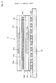
- FIG. 1 is a vertical cross-sectional view showing a schematic configuration of an electronic device according to the first embodiment.
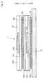
- FIG. 2 is a vertical sectional view showing a schematic configuration of an electronic device according to a second embodiment.
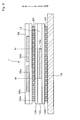
- FIG. 3 is a vertical sectional view showing a schematic configuration of an electronic device according to a third embodiment.
- FIG. 4 is a vertical sectional view showing a schematic configuration of an electronic device according to a fourth embodiment.
- FIG. 5 is a vertical sectional view showing a schematic configuration of an electronic device according to a fifth embodiment.
- FIG. 6 is a vertical sectional view showing a schematic configuration of an electronic device according to a sixth embodiment.
- FIG. 7 is a vertical sectional view showing a schematic configuration of an electronic device according to a seventh embodiment.
- FIG. 8 is a vertical sectional view showing a schematic configuration of an electronic device according to an eighth embodiment.
- FIG. 9 is a vertical sectional view showing a schematic configuration of an electronic device according to a ninth embodiment.
- the electronic device according to the embodiment of the present disclosure will be described with reference to the drawings.
- the same elements as those mentioned above will be given the same reference numerals or the same names, and the description thereof will be omitted.
- the upper package 10 side of the electronic device 1 is upward, and the printed circuit board 16 side is downward.
- the electronic device 1 As shown in FIG. 1, the electronic device 1 according to the first embodiment is a so-called PoP in which two IC packages, an upper package 10 and a lower package 12, are laminated.
- the electronic device 1 includes a printed circuit board 16 (Printed Circuit Board, hereinafter referred to as PCB), an upper package 10, and a lower package 12.
- PCB printed Circuit Board
- the upper package 10 and the lower package 12 are stacked and arranged in the vertical direction on the upper part of the PCB 16.
- the electronic device 1, the upper package 10, and the lower package 12 have a substantially rectangular shape as a flat plate.
- a plurality of upper solder balls 20 are arranged between the upper package 10 and the lower package 12.
- the upper solder ball 20 connects between the upper package 10 and the lower package 12.
- a plurality of lower solder balls 22 are arranged between the lower package 12 and the PCB 16.
- the lower solder ball 22 connects the lower package 12 and the PCB 16.
- the solder strain generated in the solder balls is proportional to the difference in the coefficient of linear expansion in the package plane direction of the connections connected by the solder balls.
- the magnitude of the solder strain generated in the upper solder ball 20 is proportional to the difference between the linear expansion coefficient ⁇ Top of the upper package 10 and the linear expansion coefficient ⁇ Bottom of the lower package 12.
- the magnitude of the solder strain generated in the lower solder ball 22 is proportional to the difference between the linear expansion coefficient ⁇ Bottom of the lower package 12 and the linear expansion coefficient ⁇ PCB of the PCB 16.
- the upper package 10 includes an upper chip 10a, an upper layer 10b, and a lower layer 10c.
- the upper chip 10a is arranged on the lower layer 10c.
- the upper surface and side surfaces of the upper chip 10a are covered with the upper layer 10b.
- the upper chip 10a is an integrated circuit or IC chip in which a plurality of transistors and wirings are mounted on a semiconductor substrate (not shown), the upper layer 10b is, for example, a mold resin, and the lower layer 10c is, for example, a printed circuit board.
- the upper tip 10a has a substantially rectangular shape as a flat plate.
- the lower package 12 includes a lower chip 12a, an upper layer 12b, an intermediate layer 12c, and a lower layer 12d.
- the lower chip 12a is arranged on the lower layer 12d.
- the upper surface and side surfaces of the lower chip 12a are covered with the intermediate layer 12c.
- An upper layer 12b is arranged on the intermediate layer 12c.
- the lower tip 12a has a substantially rectangular shape as a flat plate.
- the upper package 10 and the lower package 12 provided in the electronic device 1, and the upper chip 10a and the lower chip 12a also have a substantially rectangular shape in a plane.
- the lower chip 12a is an integrated circuit or IC chip in which a plurality of transistors and wirings are formed on a semiconductor substrate (not shown), the upper layer 12b and the lower layer 12d are, for example, a printed circuit board, and the intermediate layer 12c is, for example, a mold resin.
- the printed circuit board 16 and the upper layer 12b and the lower layer 12d which are the printed circuit boards constituting the lower package 12, are formed by arranging wirings (not shown) on a base material formed of an electrically insulating material such as resin to form a circuit.
- the electronic device 1 has a substantially rectangular shape in a plane.
- the mold resin is made of a material obtained by adding a filler such as silica to, for example, an epoxy resin which is a thermosetting resin.
- the coefficient of thermal expansion of the printed circuit board 16 is set to be larger than the coefficient of thermal expansion of the upper package 10 and the lower package 12.
- the coefficient of thermal expansion of the lower package 12 is set to be between the coefficient of thermal expansion of the upper package 10 and the coefficient of thermal expansion of the printed circuit board 16.
- the coefficient of thermal expansion of the upper package 10 is ⁇ Top
- the coefficient of thermal expansion of the lower package 12 is ⁇ Bottom
- the coefficient of thermal expansion of the printed substrate 16 is ⁇ PCB
- each thermal expansion coefficient starts from the smallest to ⁇ Top.
- ⁇ Bottom , ⁇ PCB are set to increase in this order.
- Equation (1) is a so-called Turner equation.
- ⁇ is the coefficient of linear expansion
- E is the elastic modulus
- V is the volume
- V f + V m + ... 1.
- each coefficient of thermal expansion is set so that the following equation (2) holds. ⁇ Top ⁇ Bottom ⁇ PCB ... (2)
- the coefficient of thermal expansion of the lower package 12 is set to be substantially the center of the coefficient of thermal expansion of the upper package 10 and the coefficient of thermal expansion of the printed circuit board 16.
- the absolute value of the difference between the coefficient of thermal expansion of the upper package 10 and the coefficient of thermal expansion of the lower package 12 and the difference between the coefficient of thermal expansion of the lower package 12 and the coefficient of thermal expansion of the printed substrate 16 is , 3.5 (ppm / ° C.) or less is preferable. That is, when the diameter of the upper solder ball 20 is ⁇ Top and the diameter of the lower solder ball 22 is ⁇ Bottom , the heat of the upper package 10, the lower package 12, and the printed circuit board 16 is satisfied so that the following equation (4) holds.
- the expansion coefficient is set.
- the diameter of the upper solder balls 20 arranged between the upper package 10 and the lower package 12 is arranged between the lower package 12 and the printed circuit board 16. It is set to be substantially the same as the diameter of the lower solder ball 22. Since the diameters of the upper solder ball 20 and the lower solder ball 22 are about the same, the contact area between the upper package 10 and the lower package 12, the lower package 12 and the printed circuit board 16 and the fracture resistance of the solder balls are about the same. Therefore, the crack resistance of the upper solder ball 20 and the lower solder ball 22 against solder strain is substantially the same.
- the coefficient of thermal expansion of each of the upper package 10, the lower package 12, and the printed circuit board 16 can be controlled as follows. First, if the thickness of the upper package 10, the lower package 12, and the printed circuit board 16 is increased, the coefficient of thermal expansion increases, and if the thickness is decreased, the coefficient of thermal expansion decreases. Further, the coefficient of thermal expansion can be increased by increasing the thickness of the upper layer 10b and the intermediate layer 12c made of the mold resin constituting these.
- Increasing the thickness and residual ratio of the copper foil used can increase the coefficient of thermal expansion, and decreasing these can reduce the coefficient of thermal expansion.
- the coefficient of thermal expansion of the printed circuit board 16 Since the coefficient of thermal expansion of the printed circuit board 16 is large, the rate of expansion due to thermal fluctuation is large. Since the coefficient of thermal expansion of the upper package 10 is smaller than this, the ratio of expansion due to thermal fluctuation is smaller than that of the printed circuit board 16. Therefore, when thermal fluctuation occurs, distortion occurs between the printed circuit board 16 in which the dimensional fluctuation due to expansion is large and the upper package 10 in which the dimensional fluctuation due to expansion is small, so that the coefficient of thermal expansion of the lower package 12 is higher. If it is close to either the package 10 or the printed circuit board 16, the solder strain is concentrated on either the upper solder ball 20 or the lower solder ball 22, and the solder strain becomes large, so that solder cracks occur.
- the solder strain is concentrated on the lower solder balls 22 arranged between the lower package 12 and the printed circuit board 16, so that the lower solder balls 22 are soldered. Cracks are likely to occur.
- the solder strain is concentrated on the upper solder balls 20 arranged between the upper package 10 and the lower package 12, so that the upper solder balls 20 are soldered. Cracks are likely to occur.
- the lower package 12 having the configuration described above is interposed between the upper package 10 and the printed circuit board 16.
- the strain between the upper package 10 and the printed circuit board 16 due to thermal fluctuation can be averaged by the lower package 12. Therefore, since it is possible to suppress the concentration of solder strain on either the upper solder ball 20 or the lower solder ball 22, it is possible to reduce the concentration of solder strain and suppress the occurrence of solder cracks. In this way, it is possible to provide an electronic device with improved reliability by improving the solder connection life by averaging the solder strain generated in the solder connection portion by dispersing it.
- the electronic device 1 has substantially the same configuration as that of the first embodiment, but differs in the following points.
- the upper solder ball 24 is arranged between the upper package 10 and the lower package 12 and connects between the upper package 10 and the lower package 12. Is provided.
- the diameter ⁇ Top of the upper solder ball 24 is set to be larger than the diameter ⁇ Bottom of the lower solder ball 22 arranged between the lower package 12 and the printed circuit board 16.
- the crack resistance can be ensured by increasing the size of the upper solder ball 24. That is, when the upper solder ball 24 having a large size is arranged between the upper package 10 and the lower package 12, crack resistance is improved even when the solder distortion between the upper package 10 and the lower package 12 is large. Can be secured.
- the crack resistance of the solder connection portion by the upper solder ball 24 is high even if the difference in the coefficient of thermal expansion between the upper package 10 and the lower package 12 is large. Since it is improved, the occurrence of cracks is suppressed.
- the coefficient of thermal expansion of the upper package 10 is ⁇ Top
- the coefficient of thermal expansion of the lower package 12 is ⁇ Bottom
- the coefficient of thermal expansion of the printed substrate 16 is ⁇ PCB
- the coefficient of thermal expansion is set so that the following equation (6) holds.
- the electronic device 1 according to the third embodiment shows a state in which the solder balls having a large diameter are arranged upside down with the electronic device 1 according to the second embodiment shown in FIG. There is.
- the diameter ⁇ Top of the upper solder ball 20 is smaller than the diameter ⁇ Bottom of the lower solder ball 26 arranged between the lower package 12 and the printed circuit board 16.
- the diameter of the lower solder ball 26 is larger than the diameter of the upper solder ball 20, cracks in the lower solder ball 26 do not occur even if the difference in the coefficient of thermal expansion between the lower package 12 and the printed circuit board 16 is large. It is suppressed.
- the crack resistance can be ensured by increasing the size of the lower solder ball 26. That is, when the lower solder balls 26 having a large size are arranged between the lower package 12 and the printed circuit board 16, crack resistance is improved even when the solder distortion between the lower package 12 and the printed circuit board 16 is large. Can be secured.
- the coefficient of thermal expansion is set so that the following equation (7) holds.
- ⁇ top ⁇ bottom ( ⁇ Bottom - ⁇ Top ) ⁇ ( ⁇ PCB - ⁇ Bottom )... (7) That is, when the diameter ⁇ Top of the solder ball 20 connecting the upper package and the lower package is smaller than the diameter ⁇ bottom of the solder ball 26 connecting the lower package and the printed circuit board, the coefficient of thermal expansion ⁇ Top of the upper package
- the difference between the coefficient of thermal expansion of the lower package and the coefficient of thermal expansion ⁇ Bottom of the lower package is smaller than the difference between the coefficient of thermal expansion ⁇ Bottom of the lower package and the coefficient of thermal expansion ⁇ PCB of the printed circuit board.
- the major axis of the ellipse is the diameter
- the solder crack resistance of the solder ball is proportional to the diameter of the solder ball. Therefore, the ratio of the difference in the coefficient of thermal expansion between the lower package 12 and the printed circuit board 16 to the difference in the coefficient of thermal expansion between the upper package 10 and the lower package 12 is set to be lower than the diameter ⁇ Top of the upper solder ball 24. It can be set to be substantially equal to the ratio of the diameter ⁇ Button of the solder ball 22.
- each coefficient of thermal expansion and the diameter of the upper solder ball are set so that the equation (8) holds.
- ⁇ top When ⁇ bottom , ( ⁇ Bottom - ⁇ Top ): ( ⁇ PCB - ⁇ Bottom )... (8) That is, the ratio of the diameter of the solder ball connecting between the upper package and the lower package ⁇ top to the diameter of the solder ball connecting between the lower package and the printed circuit board ⁇ bottom is the coefficient of thermal expansion ⁇ Top of the upper package and the lower. It is equal to the ratio of the difference between the coefficient of thermal expansion ⁇ Bottom of the lower package and the coefficient of thermal expansion ⁇ PCB of the printed circuit board to the difference from the coefficient of thermal expansion ⁇ Bottom of the package.
- the upper solder ball 24 or the lower solder ball 26 is cracked at the solder connection portion according to the difference in the coefficient of thermal expansion between the upper package 10, the lower package 12, and the printed circuit board 16, that is, the magnitude of the solder strain. It can be arranged so as to ensure the sex. That is, the size of the upper solder ball 24 or the lower solder ball 26 is increased in the place where the difference in the coefficient of thermal expansion between the upper package 10, the lower package 12, and the printed circuit board 16 is large, that is, the place where the solder strain is large, and the solder is soldered.
- the crack resistance of the connecting portion can be improved. Therefore, the crack resistance of the electronic device 1 can be efficiently improved.
- the same effect as that of the electronic device 1 according to the first embodiment is obtained.
- the electronic device 1 according to the fourth embodiment will be described with reference to FIG.
- the horizontal dimension L Top of the upper package 30 arranged on the upper side of the electronic device 1 is set to be smaller than the horizontal dimension L Bottom of the lower package 12 arranged on the lower side.
- the dimensional fluctuation due to the thermal fluctuation of the package becomes larger as the horizontal dimension of the package is larger. Therefore, the solder strain in a package having a large horizontal dimension is larger than that in a package having a small horizontal dimension.
- the horizontal dimension L Bottom of the lower package 12 arranged on the lower side is larger than the horizontal dimension L Top of the upper package 30. Therefore, the solder strain in the lower solder ball 22 of the lower package 12 is larger than the solder strain in the upper solder ball 20 of the upper package 30.
- the difference between the coefficient of thermal expansion of the upper package and the coefficient of thermal expansion of the lower package Is set to be larger than the difference between the coefficient of thermal expansion of the lower package and the coefficient of thermal expansion of the printed substrate.
- the coefficient of thermal expansion is set so that the following equation (9) holds.
- L Top ⁇ L Bottom ( ⁇ Bottom - ⁇ Top )> ( ⁇ PCB - ⁇ Bottom )... (9) That is, when the horizontal dimension L Bottom of the lower package 12 is larger than the horizontal dimension L Top of the upper package 30, the difference between the coefficient of thermal expansion ⁇ Top of the upper package and the coefficient of thermal expansion ⁇ Bottom of the lower package is the lower package. It is larger than the difference between the coefficient of thermal expansion ⁇ Bottom and the coefficient of thermal expansion ⁇ PCB of the printed substrate.
- the solder strain is proportional to the lateral dimension of the package. Therefore, the ratio of the horizontal dimension L Top of the upper package 30 to the horizontal dimension L Bottom of the lower package 12 is made to be substantially equal to the ratio of the difference between the coefficient of thermal expansion of the upper package 30 and the coefficient of thermal expansion of the lower package 12. By setting the coefficient of thermal expansion to, the solder strain can be averaged.
- the coefficient of thermal expansion is set so that the following equation (10) holds.
- L Top In the case of L Bottom , ( ⁇ Bottom - ⁇ Top )> ( ⁇ PCB - ⁇ Bottom )... (10) That is, the ratio of the lateral dimension L Bottom of the lower package in the lateral dimension L Top of the upper package, the thermal expansion coefficient of the lower package for the difference between the thermal expansion coefficient alpha Bottom thermal expansion coefficient alpha Top and bottom package on package alpha Bottom Is equal to the ratio of the difference between the coefficient of thermal expansion of the printed substrate and the coefficient of thermal expansion ⁇ PCB .
- the same effect as that of the electronic device 1 according to the first embodiment is obtained.
- the electronic device 1 according to the fifth embodiment will be described.
- the lower package 32 has a multilayer structure including a lower chip 32a, an upper layer 32b, an intermediate layer 32c, and a lower layer 32d. Similar to the first to fourth embodiments, it is assumed that the coefficient of thermal expansion of the printed circuit board 16 is larger than the coefficient of thermal expansion of the upper package 10 in the fifth embodiment as well.
- the coefficient of thermal expansion of the lower layer 32d is set to be larger than the coefficient of thermal expansion of the upper layer 32b.
- the coefficient of thermal expansion of the upper layer 32b is set to be smaller than the coefficient of thermal expansion of the lower layer 32d.
- the upper layer 32b having a small coefficient of thermal expansion is connected to the upper package 10 having a small coefficient of thermal expansion via the upper solder ball 20, and the lower layer 32d having a large coefficient of thermal expansion is connected to the printed substrate 16 having a large coefficient of thermal expansion. Since they are connected via the lower solder balls 22, the difference in the coefficient of thermal expansion becomes smaller in the connection region of the upper solder balls 20 and 22. This makes it possible to average the solder strain.
- the coefficient of thermal expansion is set so that the following equation (11) holds.
- ⁇ Top ⁇ Bottom ⁇ PCB ⁇ Bottom up ⁇ Bottom low ...
- ⁇ Bottom up is the coefficient of thermal expansion of the upper layer 32b of the lower package 32
- ⁇ Bottom low is the coefficient of thermal expansion of the lower layer 32d.
- the same effect as that of the electronic device 1 according to the first embodiment is obtained.
- the electronic device 1 according to the sixth embodiment will be described.
- the upper package 10 and the lower chip 10a and the lower chip 12a have the same length in the longitudinal direction and the end position S in the longitudinal direction.
- Package 12 is arranged.
- the warped shapes of the upper package 10 and the upper solder ball 20 due to thermal fluctuation can be matched, so that the solder crack resistance of the solder connection portion between the upper package 10 and the lower package 12 can be improved.
- the electronic device 1 according to the seventh embodiment will be described.
- the upper package 10 and the lower chip 10a and the lower chip 12a are aligned with each other so that the length in the longitudinal direction and the end position G in the longitudinal direction match.
- Package 12 is placed.
- a solder ball missing portion 33 in which no solder ball is present is provided between the upper package 10 and the lower package 12 and between the lower package 12 and the printed circuit board 16 in accordance with the end position G.
- solder ball missing portion 33 is provided at the end position G where the solder strain is locally increased, solder cracks near the end position G can be suppressed.
- the electronic device 1 according to the eighth embodiment will be described.
- the upper package 36 includes an upper chip 36a and an upper chip 36b in parallel inside in the lateral direction. Then, the substantially central portion of the upper chip 36a and the upper chip 36b is arranged so as to coincide with the end position H of the lower chip 12a of the lower package 12.
- the electronic device 1 according to the ninth embodiment will be described.
- the upper package 40 and the upper package 42 are provided on the lower package 12.
- the upper package 40 includes an upper chip 40a, an upper layer 40b, and a lower layer 40c.
- the upper package 42 includes an upper chip 42a, an upper layer 42b, and a lower layer 42c.
- the upper package 40 and the upper package 42 are arranged side by side in the horizontal direction on the lower package 12. At this time, the central portions of the upper package 40, the upper chip 40a, the upper package 42, and the upper chip 42a are arranged so as to coincide with the end position H of the lower chip 12a.
- the upper package 40 and the upper tip 40a, and the upper package 42 and the upper tip 42a are rigid, so that the warp of the lower tip 12a of the lower package 12 at the end position H can be suppressed. .. Therefore, this makes it possible to reduce the solder distortion of the electronic device 1.
Landscapes
- Engineering & Computer Science (AREA)
- Microelectronics & Electronic Packaging (AREA)
- Electric Connection Of Electric Components To Printed Circuits (AREA)
- Structures For Mounting Electric Components On Printed Circuit Boards (AREA)
Priority Applications (2)
| Application Number | Priority Date | Filing Date | Title |
|---|---|---|---|
| CN202080024606.2A CN113632227A (zh) | 2019-03-28 | 2020-03-11 | 电子装置 |
| US17/481,783 US11974398B2 (en) | 2019-03-28 | 2021-09-22 | Electronic device |
Applications Claiming Priority (2)
| Application Number | Priority Date | Filing Date | Title |
|---|---|---|---|
| JP2019063315A JP7056620B2 (ja) | 2019-03-28 | 2019-03-28 | 電子装置 |
| JP2019-063315 | 2019-03-28 |
Related Child Applications (1)
| Application Number | Title | Priority Date | Filing Date |
|---|---|---|---|
| US17/481,783 Continuation US11974398B2 (en) | 2019-03-28 | 2021-09-22 | Electronic device |
Publications (1)
| Publication Number | Publication Date |
|---|---|
| WO2020195836A1 true WO2020195836A1 (ja) | 2020-10-01 |
Family
ID=72611369
Family Applications (1)
| Application Number | Title | Priority Date | Filing Date |
|---|---|---|---|
| PCT/JP2020/010549 Ceased WO2020195836A1 (ja) | 2019-03-28 | 2020-03-11 | 電子装置 |
Country Status (4)
| Country | Link |
|---|---|
| US (1) | US11974398B2 (https=) |
| JP (1) | JP7056620B2 (https=) |
| CN (1) | CN113632227A (https=) |
| WO (1) | WO2020195836A1 (https=) |
Families Citing this family (1)
| Publication number | Priority date | Publication date | Assignee | Title |
|---|---|---|---|---|
| JP2024085812A (ja) | 2022-12-15 | 2024-06-27 | 株式会社デンソー | 電子装置 |
Citations (5)
| Publication number | Priority date | Publication date | Assignee | Title |
|---|---|---|---|---|
| JPH03105954A (ja) * | 1989-09-20 | 1991-05-02 | Hitachi Ltd | 半導体装置 |
| JP2000323602A (ja) * | 1999-05-07 | 2000-11-24 | Toshiba Corp | 配線回路装置 |
| JP2004103665A (ja) * | 2002-09-05 | 2004-04-02 | Toshiba Corp | 電子デバイスモジュール |
| JP2004356620A (ja) * | 2003-03-19 | 2004-12-16 | Ngk Spark Plug Co Ltd | 中継基板、半導体素子付き中継基板、中継基板付き基板、半導体素子と中継基板と基板とからなる構造体 |
| JP2006313800A (ja) * | 2005-05-09 | 2006-11-16 | Matsushita Electric Ind Co Ltd | 半導体装置における実装構造の接続信頼性の予測方法およびその半導体装置 |
Family Cites Families (10)
| Publication number | Priority date | Publication date | Assignee | Title |
|---|---|---|---|---|
| JPH10247706A (ja) * | 1997-03-05 | 1998-09-14 | Sumitomo Kinzoku Electro Device:Kk | ボールグリッドアレイパッケージ |
| JP2000260912A (ja) * | 1999-03-05 | 2000-09-22 | Fujitsu Ltd | 半導体装置の実装構造及び半導体装置の実装方法 |
| US6940176B2 (en) * | 2002-05-21 | 2005-09-06 | United Microelectronics Corp. | Solder pads for improving reliability of a package |
| TW563895U (en) * | 2003-03-06 | 2003-11-21 | Advanced Semiconductor Eng | Thin type ball grid array package |
| JP2004356618A (ja) | 2003-03-19 | 2004-12-16 | Ngk Spark Plug Co Ltd | 中継基板、半導体素子付き中継基板、中継基板付き基板、半導体素子と中継基板と基板とからなる構造体、中継基板の製造方法 |
| KR100839075B1 (ko) * | 2007-01-03 | 2008-06-19 | 삼성전자주식회사 | 아이씨 패키지 및 그 제조방법 |
| JP5961625B2 (ja) | 2011-11-10 | 2016-08-02 | パナソニック株式会社 | 半導体装置 |
| JP2016162815A (ja) | 2015-02-27 | 2016-09-05 | 株式会社ジェイテクト | 半導体部品及び半導体部品の製造方法 |
| US10700030B2 (en) * | 2018-08-14 | 2020-06-30 | Taiwan Semiconductor Manufacturing Co., Ltd. | Semiconductor package having varying conductive pad sizes |
| JP2020167181A (ja) * | 2019-03-28 | 2020-10-08 | 株式会社デンソー | 電子装置 |
-
2019
- 2019-03-28 JP JP2019063315A patent/JP7056620B2/ja active Active
-
2020
- 2020-03-11 WO PCT/JP2020/010549 patent/WO2020195836A1/ja not_active Ceased
- 2020-03-11 CN CN202080024606.2A patent/CN113632227A/zh not_active Withdrawn
-
2021
- 2021-09-22 US US17/481,783 patent/US11974398B2/en active Active
Patent Citations (5)
| Publication number | Priority date | Publication date | Assignee | Title |
|---|---|---|---|---|
| JPH03105954A (ja) * | 1989-09-20 | 1991-05-02 | Hitachi Ltd | 半導体装置 |
| JP2000323602A (ja) * | 1999-05-07 | 2000-11-24 | Toshiba Corp | 配線回路装置 |
| JP2004103665A (ja) * | 2002-09-05 | 2004-04-02 | Toshiba Corp | 電子デバイスモジュール |
| JP2004356620A (ja) * | 2003-03-19 | 2004-12-16 | Ngk Spark Plug Co Ltd | 中継基板、半導体素子付き中継基板、中継基板付き基板、半導体素子と中継基板と基板とからなる構造体 |
| JP2006313800A (ja) * | 2005-05-09 | 2006-11-16 | Matsushita Electric Ind Co Ltd | 半導体装置における実装構造の接続信頼性の予測方法およびその半導体装置 |
Also Published As
| Publication number | Publication date |
|---|---|
| US11974398B2 (en) | 2024-04-30 |
| JP2020167182A (ja) | 2020-10-08 |
| US20220007510A1 (en) | 2022-01-06 |
| JP7056620B2 (ja) | 2022-04-19 |
| CN113632227A (zh) | 2021-11-09 |
Similar Documents
| Publication | Publication Date | Title |
|---|---|---|
| US6992896B2 (en) | Stacked chip electronic package having laminate carrier and method of making same | |
| KR101341273B1 (ko) | 반도체 패키지 및 당해 반도체 패키지의 실장구조 | |
| US20060023439A1 (en) | Stacked chip electronic package having laminate carrier and method of making same | |
| CN110875291A (zh) | 基板组件、半导体封装件和制造该半导体封装件的方法 | |
| US20070132072A1 (en) | Chip package and coreless package substrate thereof | |
| JP2008071953A (ja) | 半導体装置 | |
| CN104966702A (zh) | 半导体封装件 | |
| US20040099958A1 (en) | Crack resistant interconnect module | |
| WO2018235715A1 (ja) | モジュールおよびその製造方法 | |
| JP2013219170A (ja) | 基板装置 | |
| CN116130448A (zh) | 电子封装件及其封装基板 | |
| US9661762B2 (en) | Printed wiring board | |
| KR20210017271A (ko) | 반도체 패키지 | |
| JP7056620B2 (ja) | 電子装置 | |
| US11848146B2 (en) | Stacked electronic module and method to make the same | |
| US8829361B2 (en) | Wiring board and mounting structure using the same | |
| US10314166B2 (en) | Printed wiring board | |
| JP7226358B2 (ja) | 電子機器 | |
| KR100546359B1 (ko) | 동일 평면상에 횡 배치된 기능부 및 실장부를 구비하는 반도체 칩 패키지 및 그 적층 모듈 | |
| JP2008205290A (ja) | 部品内蔵基板及びその製造方法 | |
| KR20240108500A (ko) | 스티프너 부착 배선 기판 | |
| US20220415777A1 (en) | Semiconductor package | |
| KR20140078291A (ko) | 인쇄회로기판 | |
| JP2011166096A (ja) | 表面実装デバイス及びプリント基板、並びに、それらを用いた表面実装デバイスの実装構造体 | |
| CN102473689B (zh) | 具有彼此绝缘电源侧和接地侧金属加固部件的半导体器件 |
Legal Events
| Date | Code | Title | Description |
|---|---|---|---|
| 121 | Ep: the epo has been informed by wipo that ep was designated in this application |
Ref document number: 20777145 Country of ref document: EP Kind code of ref document: A1 |
|
| NENP | Non-entry into the national phase |
Ref country code: DE |
|
| 122 | Ep: pct application non-entry in european phase |
Ref document number: 20777145 Country of ref document: EP Kind code of ref document: A1 |