WO2020194409A1 - 発光素子 - Google Patents
発光素子 Download PDFInfo
- Publication number
- WO2020194409A1 WO2020194409A1 PCT/JP2019/012251 JP2019012251W WO2020194409A1 WO 2020194409 A1 WO2020194409 A1 WO 2020194409A1 JP 2019012251 W JP2019012251 W JP 2019012251W WO 2020194409 A1 WO2020194409 A1 WO 2020194409A1
- Authority
- WO
- WIPO (PCT)
- Prior art keywords
- light emitting
- functional group
- skeleton
- atom
- polysilsesquioxane
- Prior art date
- Legal status (The legal status is an assumption and is not a legal conclusion. Google has not performed a legal analysis and makes no representation as to the accuracy of the status listed.)
- Ceased
Links
Images





Classifications
-
- H—ELECTRICITY
- H10—SEMICONDUCTOR DEVICES; ELECTRIC SOLID-STATE DEVICES NOT OTHERWISE PROVIDED FOR
- H10K—ORGANIC ELECTRIC SOLID-STATE DEVICES
- H10K85/00—Organic materials used in the body or electrodes of devices covered by this subclass
- H10K85/40—Organosilicon compounds, e.g. TIPS pentacene
-
- C—CHEMISTRY; METALLURGY
- C09—DYES; PAINTS; POLISHES; NATURAL RESINS; ADHESIVES; COMPOSITIONS NOT OTHERWISE PROVIDED FOR; APPLICATIONS OF MATERIALS NOT OTHERWISE PROVIDED FOR
- C09K—MATERIALS FOR MISCELLANEOUS APPLICATIONS, NOT PROVIDED FOR ELSEWHERE
- C09K11/00—Luminescent materials, e.g. electroluminescent or chemiluminescent
- C09K11/08—Luminescent materials, e.g. electroluminescent or chemiluminescent containing inorganic luminescent materials
- C09K11/88—Luminescent materials, e.g. electroluminescent or chemiluminescent containing inorganic luminescent materials containing selenium, tellurium or unspecified chalcogen elements
- C09K11/881—Chalcogenides
- C09K11/883—Chalcogenides with zinc or cadmium
-
- H—ELECTRICITY
- H05—ELECTRIC TECHNIQUES NOT OTHERWISE PROVIDED FOR
- H05B—ELECTRIC HEATING; ELECTRIC LIGHT SOURCES NOT OTHERWISE PROVIDED FOR; CIRCUIT ARRANGEMENTS FOR ELECTRIC LIGHT SOURCES, IN GENERAL
- H05B33/00—Electroluminescent light sources
- H05B33/12—Light sources with substantially two-dimensional [2D] radiating surfaces
- H05B33/14—Light sources with substantially two-dimensional [2D] radiating surfaces characterised by the chemical or physical composition or the arrangement of the electroluminescent material, or by the simultaneous addition of the electroluminescent material in or onto the light source
-
- H—ELECTRICITY
- H05—ELECTRIC TECHNIQUES NOT OTHERWISE PROVIDED FOR
- H05B—ELECTRIC HEATING; ELECTRIC LIGHT SOURCES NOT OTHERWISE PROVIDED FOR; CIRCUIT ARRANGEMENTS FOR ELECTRIC LIGHT SOURCES, IN GENERAL
- H05B33/00—Electroluminescent light sources
- H05B33/12—Light sources with substantially two-dimensional [2D] radiating surfaces
- H05B33/20—Light sources with substantially two-dimensional [2D] radiating surfaces characterised by the chemical or physical composition or the arrangement of the material in which the electroluminescent material is embedded
-
- H—ELECTRICITY
- H10—SEMICONDUCTOR DEVICES; ELECTRIC SOLID-STATE DEVICES NOT OTHERWISE PROVIDED FOR
- H10K—ORGANIC ELECTRIC SOLID-STATE DEVICES
- H10K85/00—Organic materials used in the body or electrodes of devices covered by this subclass
- H10K85/10—Organic polymers or oligomers
- H10K85/141—Organic polymers or oligomers comprising aliphatic or olefinic chains, e.g. poly N-vinylcarbazol, PVC or PTFE
-
- H—ELECTRICITY
- H10—SEMICONDUCTOR DEVICES; ELECTRIC SOLID-STATE DEVICES NOT OTHERWISE PROVIDED FOR
- H10K—ORGANIC ELECTRIC SOLID-STATE DEVICES
- H10K2101/00—Properties of the organic materials covered by group H10K85/00
- H10K2101/30—Highest occupied molecular orbital [HOMO], lowest unoccupied molecular orbital [LUMO] or Fermi energy values
-
- H—ELECTRICITY
- H10—SEMICONDUCTOR DEVICES; ELECTRIC SOLID-STATE DEVICES NOT OTHERWISE PROVIDED FOR
- H10K—ORGANIC ELECTRIC SOLID-STATE DEVICES
- H10K50/00—Organic light-emitting devices
- H10K50/10—OLEDs or polymer light-emitting diodes [PLED]
- H10K50/11—OLEDs or polymer light-emitting diodes [PLED] characterised by the electroluminescent [EL] layers
- H10K50/115—OLEDs or polymer light-emitting diodes [PLED] characterised by the electroluminescent [EL] layers comprising active inorganic nanostructures, e.g. luminescent quantum dots
Definitions
- the present invention relates to a light emitting device.
- QLED quantum dot
- FIG. 17 is a diagram showing conventional nanoparticles and a conventional film in which quantum dots are sealed with a chemically and thermally stable material.
- FIG. 17A is a diagram showing a schematic configuration of nanoparticles 100 disclosed in Non-Patent Documents 1 and 2
- FIG. 17B is a diagram showing a schematic structure of nanoparticles 100
- FIG. 17B is a silica layer contained in nanoparticles 100. It is a figure which shows 103.
- the nanoparticles 100 were formed so as to cover the quantum dots 101, the siloxane monolayer 102 coordinated on the surface of the quantum dots 101, and the siloxane monolayer 102. Includes a silica layer 103.
- FIG. 17A the nanoparticles 100 were formed so as to cover the quantum dots 101, the siloxane monolayer 102 coordinated on the surface of the quantum dots 101, and the siloxane monolayer 102. Includes a silica layer 103.
- FIG. 17A the nanoparticles 100
- FIG. 17C is a diagram showing a schematic configuration of the film 110 including the quantum dots 111 disclosed in Patent Document 1, in which the film 110 is coordinated with the quantum dots 111 and on the surfaces of the quantum dots 111. Includes a silica layer 112 formed with trialkoxysilane.
- FIG. 17D is a diagram showing a schematic configuration of nanoparticles 120 disclosed in Patent Document 2.
- the nanoparticles 120 are composed of quantum dots 121 made of Si constituting a core and silica constituting a shell. Includes layer 122 and.
- the quantum dots are sealed with silica, which is a chemically and thermally stable material, the durability of the quantum dots is improved. Can be improved.
- Non-Patent Document 1 Non-Patent Document 2
- Patent Document 1 Patent Document 2
- Patent Document 2 silica is used as a material for sealing the quantum dots.
- Such silica-sealed quantum dots can be excited by light to emit light, but since silica is an insulator with a large bandgap, it is necessary to inject electrons and holes to emit light. However, there is a problem that a very large voltage is required.
- the present invention has been made in view of the above problems, and an object of the present invention is to provide a light emitting device capable of injecting electrons and holes with a relatively small voltage to emit light and having high durability.
- the light emitting element of the present invention is a light emitting element including a first electrode, a second electrode, and a light emitting layer provided between the first electrode and the second electrode in order to solve the above-mentioned problems.
- the light emitting layer contains quantum dots and a conductive first polysilsesquioxane.
- the light emitting element it is possible to realize a light emitting element that can emit light by injecting electrons and holes with a relatively small voltage and has high durability.
- a light emitting element capable of injecting electrons or holes with a relatively small voltage to emit light and having high durability.
- (A) is a diagram showing a schematic configuration of nanoparticles contained in the light emitting layer of the light emitting element of the first embodiment, and (b) is coordinated to quantum dots of the first polysilsesquioxane having conductivity. It is a figure which shows the functional group part
- FIG. 3C is a figure which shows the schematic structure of the 1st polysilsesquioxane which has conductivity.
- (A) is a diagram for explaining a method for synthesizing silica, and (b) is a diagram for explaining a method for synthesizing a second polysilsesquioxane having a functional group coordinated to a quantum dot, (c).
- (A) is a diagram showing an example of a silane containing a functional group coordinated to a quantum dot having an amino group
- (b) is an example of a silane containing a functional group coordinating to a quantum dot having a thiol group. It is a figure which shows.
- (A), (b) and (c) are diagrams showing an example of a ligand coordinated to a quantum dot.
- (A), (b), (c), (d), (e), (f), (g) and (h) are diagrams showing an example of a functional group responsible for conductivity.
- (A) is a diagram for explaining a method for synthesizing a silane containing a functional group responsible for conductivity
- (b) is a conductivity synthesized from a silane containing a functional group responsible for conductivity shown in (a). It is a figure which shows an example of the 1st polysilsesquioxane which has.
- (A) and (b) are diagrams showing an example of a silane that can be mixed during the synthesis of a conductive first polysilsesquioxane or a second polysilsesquioxane having a functional group coordinated to a quantum dot. Is.
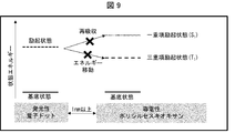
- (A) is a diagram for explaining reabsorption and energy transfer that occur when the excited state energy of the conductive first polysilsesquioxane is lower than the excited state energy of the quantum dots
- (b). ) Is a diagram for explaining the reason why reabsorption and energy transfer do not occur when the energy of the excited state of the conductive first polysilsesquioxane is higher than the energy of the excited state of the quantum dots.
- the energy of the singlet excited state of the conductive first polysilsesquioxane is higher than the energy of the excited state of the quantum dots, and the distance between the conductive first polysilsesquioxane and the quantum dots.
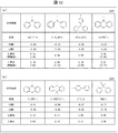
- (A) and (b) are examples of functional groups which are responsible for conductivity, and are diagrams showing the HOMO level, LUMO level, singlet excitation level and triplet excitation level. It is still another example of the functional group which bears conductivity, and is the figure which shows the HOMO level, LUMO level, singlet excitation level and triplet excitation level. It is a figure which shows the schematic structure of the light emitting element of Embodiment 1.
- (A) is a diagram showing a schematic configuration of a light emitting device of the second embodiment
- (b) is a diagram showing a schematic configuration of nanoparticles provided in the light emitting element of the second embodiment
- (A) is a diagram showing a schematic configuration of a light emitting device of the third embodiment
- (b) is a diagram showing a schematic configuration of nanoparticles provided in the light emitting device of the third embodiment.
- It is a figure for demonstrating the synthesis method of the 1st polysilsesquioxane which has a conductivity in a light emitting layer provided in the light emitting element of Embodiment 3.
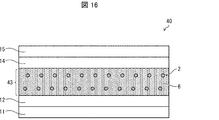
- FIG. It is a figure which shows the schematic structure of the light emitting element of Embodiment 4.
- (A), (b) and (d) are diagrams showing conventional nanoparticles in which quantum dots are sealed with a chemically and thermally stable material
- (c) is a diagram showing quantum dots chemically and thermally. It is a figure which shows the conventional film sealed with the thermally stable material.
- FIGS. 1 to 16 An embodiment of the present invention will be described as follows with reference to FIGS. 1 to 16.
- the same reference numerals may be added to the configurations having the same functions as the configurations described in the specific embodiments, and the description thereof may be omitted.
- FIG. 12 is a diagram showing a schematic configuration of the light emitting element 10 of the first embodiment.
- the light emitting element 10 includes a first electrode 11, a second electrode 15, and a light emitting layer 13 including nanoparticles 1 provided between the first electrode 11 and the second electrode 15. It has. Further, the light emitting element 10 is provided with a first carrier transport layer 12 between the first electrode 11 and the light emitting layer 13, and a second carrier transport layer 14 between the light emitting layer 13 and the second electrode 15. There is.
- a plurality of light emitting elements 10 are formed on an active matrix substrate provided with a plurality of thin film transistor elements (TFT elements) (not shown) according to the resolution of the display device, and are provided on each light emitting element 10.
- the first electrode 11 is electrically connected to the drain electrode of the thin film transistor element.
- the first electrode 11, the first carrier transport layer 12, the light emitting layer 13, the second carrier transport layer 14, and the second electrode 15 are formed on the active matrix substrate in this order.
- the second electrode 15, the second carrier transport layer 14, the light emitting layer 13, and the first carrier transport layer are placed on the active matrix substrate. 12 and the first electrode 11 may be formed in this order.
- the light emitting layer 13 in the light emitting element 10 emits light in the first wavelength region. Then, on the active matrix substrate, in addition to the light emitting element 10 that emits light in the first wavelength region, a light emitting layer that emits light in a second wavelength region whose center wavelength is different from that of the first wavelength region is provided. At least a light emitting element and a light emitting element provided with a light emitting layer that emits light in a third wavelength region whose central wavelengths are different from those in the first wavelength region and the second wavelength region are formed. Four or more types of light emitting elements that emit light in such wavelength regions different from each other may be formed.
- the particle size of the quantum dots may be different in each light emitting layer, and different types of quantum dots may be used. May be used.
- the light emitting layer 13 that emits light in the first wavelength region contains the quantum dots 2 and the conductive first polysilsesquioxane 3
- the light in the second wavelength region will be described.
- the light emitting layer of the light emitting element that emits light and the light emitting layer of the light emitting element that emits light in the third wavelength region may also contain quantum dots and the first polysilsesquioxane 3 having conductivity. Good.
- a metal material having a high reflectance of visible light for example, Al, Cu, Au, Ag, etc.
- the reflectance of visible light is high, for example, ITO (Indium Tin Oxide) and an alloy containing Ag may be laminated and used as the first electrode 11.
- the second electrode 15 is a material having a high visible light transmittance (transparent conductive film material), for example, ITO (Indium Tin Oxide), IZO (Indium Zinc Oxide), ZnO, AZO (aluminum-doped zinc oxide). , BZO (boron-doped zinc oxide) and the like can be used.
- the light emitting element 10 when the light emitting element 10 is of the bottom emission type, a material having a high visible light transmittance (transparent conductive film material) can be used as the first electrode 11, and the second electrode 15 is visible. If a metal material having a high light transmittance or a high visible light reflectance is used, for example, ITO (Indium Tin Oxide) and an alloy containing Ag may be laminated and used.
- ITO Indium Tin Oxide
- the first electrode 11 is the anode (anode electrode) and the second electrode 15 is the cathode (cathode electrode)
- the first electrode 11 and the light emitting layer 13 The first carrier transport layer 12 between them is a hole transport layer (Hole Transport Layer)
- the second carrier transport layer 14 between the light emitting layer 13 and the second electrode 15 is an electron transport layer (Electron Transport Layer).
- the light emitting element 10 may include a hole injection layer between the first electrode 11 and the first carrier transport layer 12 which is a hole transport layer, and the second carrier transport layer 14 which is an electron transport layer.
- An electron injection layer may be provided between the second electrode 15 and the second electrode 15.
- an electron blocking layer may be provided between the first carrier transport layer 12 which is a hole transport layer and the light emitting layer 13, and the light emitting layer 13 and the second carrier transport layer 14 which is an electron transport layer
- a hole blocking layer may be provided between them.
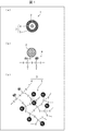
- FIG. 1 (a) is a diagram showing a schematic configuration of nanoparticles 1 contained in the light emitting layer 13 of the light emitting element 10, and FIG. 1 (b) is a conductive first polysilsesquioxane 3 It is a figure which shows the functional group part 4 coordinated with the quantum dot 2 of FIG. 1, and (c) of FIG. 1 is a figure which shows the schematic structure of the 1st polysilsesquioxane 3 which has conductivity.
- the nanoparticles 1 include quantum dots 2 (also referred to as phosphor quantum dots) and a conductive first polysilsesquioxane 3.
- quantum dots 2 also referred to as phosphor quantum dots
- a conductive first polysilsesquioxane 3 As a specific material of the quantum dot 2, for example, any one of CdSe / CdS, CdSe / ZnS, InP / ZnS, ZnSe / ZnS, CIGS / ZnS, AgInS2 / GaS and lead halide perovskite can be used.
- the particle size of the quantum dots is about 3 to 10 nm.
- the conductive first polysilsesquioxane 3 includes a functional group portion 4 coordinated to the quantum dots 2 and a functional group portion 5 responsible for the conductivity of the first polysilsesquioxane 3.
- the functional group portion 4 coordinated to the quantum dot 2 in the conductive first polysilsesquioxane 3 has a functional group R1 coordinated to the quantum dot 2. is there.
- the conductive first polysilsesquioxane 3 has a functional group portion 4 coordinated to the quantum dot 2 having a functional group R1 coordinated to the quantum dot 2.
- the polysilsesquioxane having both the functional group portion 5 responsible for the conductivity of the first polysilsesquioxane 3 having the functional group R2 responsible for the conductivity.
- the conductive first polysilsesquioxane 3 is arranged so as to surround the quantum dots 2 and protects the quantum dots 2.
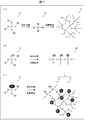
- FIG. 2A is a diagram illustrating a method for synthesizing silica C
- FIG. 2B is a diagram for synthesizing a second polysilsesquioxane 4P having a functional group R1 coordinated to quantum dots 2. It is a figure explaining the method
- (c) of FIG. 2 is a figure explaining the method of synthesizing the first polysilseskioxane 3 having conductivity.
- tetraalkoxysilane A (R3 in the figure is an alkyl group such as methyl or ethyl) is hydrolyzed under an acid / base catalyst to form a silanol group.
- Silane C having a three-dimensional structure can be produced by obtaining a silane B having a silane B and condensing the silane B having a silanol group by heating.
- Silica C is a chemically and thermally stable material, but is not preferable as a material for protecting quantum dots 2 because it is an insulator having a large band gap.
- a trialkoxysilane D having a functional group R1 coordinated to the quantum dot 2 (R3 in the figure is, for example, an alkyl group such as methyl or ethyl.
- the functional group R1 that coordinates the quantum dot 2 is coordinated to the surface of the quantum dot 2, that is, the functional group R1 that coordinates the quantum dot 2 of the trialkoxysilane D molecule faces the quantum dot 2.
- it can be hydrolyzed and heat-condensed under an acid / base catalyst to form a monomolecular film of the second polysilsesquioxane 4P having a three-dimensional structure surrounding the quantum dots 2.
- a trialkoxysilane E having a functional group R2 responsible for conductivity (R3 in the figure is, for example, an alkyl group such as methyl or ethyl) is added.
- the functional group portion 4 coordinated to the quantum dot 2 and the functional group portion 5 responsible for conductivity are silanols of silane having a silanol group of the second polysilsesquioxane 4P and a functional group R2 responsible for conductivity. Since it condenses with the group, it is chemically bonded.
- the first polysilsesquioxane 3 In the step of synthesizing the first polysilsesquioxane 3 having both the functional group portion 4 coordinated to the quantum dot 2 and the functional group portion 5 responsible for conductivity, the first polysilsesquioxane 3 is used.
- Trialkoxysilane E having a functional group R2 (including a partially silanol-based one) and the like are also mixed.
- Polysilsesquioxane is a trialkoxysilane having a functional group directly bonded to a Si atom (silicon element) (tetraalkoxysilane, a dialkoxysilane having a functional group directly bonded to a Si atom, and a Si atom).
- a polymer having a functional group directly bonded to a Si atom generated from may include monoalkoxysilane having a directly bonded functional group, etc.) and having a siloxane bond (Si—O—Si) as a main chain. Refers to the product.
- FIG. 3A is a diagram showing an example of a silane containing a functional group R1 coordinated to a quantum dot 2 having an amino group
- FIG. 3B is a diagram showing an example of a silane coordinated to a quantum dot 2 having a thiol group. It is a figure which shows an example of the silane containing the functional group R1 which is positioned.
- the trialkoxysilane D having the functional group R1 coordinated to the quantum dot 2 shown in FIG. 2 (b) for example, 3-aminopropyltriethoxysilane and / and the figure shown in FIG. 3 (a).
- 3- (Triethoxysilyl) propanethiol shown in 3 (b) can be used.
- FIG. 4 are diagrams showing an example of a ligand coordinated to the quantum dot 2.
- Examples of the functional group coordinated on the surface of a semiconductor quantum dot of Group II-VI such as CdSe or Group III-V such as InP used as a material of the quantum dot 2 include an amino group, a thiol group, an alkoxy group and a carboxy group.
- Groups, phosphino groups, oxidized phosphino groups, imidazolium groups, pyridinyl groups and the like are known (see Coordination Chemistry Reviews 320-321 (2016) 216-237). It is considered that the functional group R1 coordinated to the quantum dot 2 is ionized and coordinated to the quantum dot 2.
- FIG. 4 shows an example of an anion-type ligand coordinated to the quantum dot 2.
- the anion-type ligand coordinated to the quantum dot 2 include a ligand containing at least one selected from carboxylate, alkoxylate, thiolate, dithiolate, phosphylate, phosphonate, and phosphoric anhydride.
- (B) of FIG. 4 shows an example of a neutral electron donor type ligand.
- the neutral electron donor type ligand coordinated to the quantum dot 2 include a ligand containing at least one selected from 1 to tertiary amine, 2 to 3 phosphine, phosphinic acid, imidazole, and pyridine. ..
- FIG. 4C shows an example of an inorganic ligand.
- the inorganic ligand, Cl -, Br -, I -, S 2-, Se 2-, Te 2-, K +, can be selected at least one of NH 4 +.
- FIG. 4 show silane or an alkyl group bonded to silane. Not all ligands coordinated to the quantum dots 2 may be directly or indirectly bound to the silane, and for example, an inorganic ligand as shown in FIG. 4C may be coordinated.
- the ratio of the anion, the carboxylate anion, the phosphinolate cation, the oxidized phosphinolate cation and the like is preferably 0.1% or more and 50% or less in terms of molar ratio with respect to the Si atom, and 0.1% or more and 20 It is more preferably% or less. This is because if it exceeds 50%, there may be a surplus ligand that does not coordinate to the quantum dot.
- FIGS. 5A to 5H are diagrams showing an example of the functional group R2 responsible for conductivity. At least one functional group R2 is selected from the functional groups shown in FIGS. 5A to 5H.
- Polysilsesquioxane (PSQ) having a functional group containing a carbazole skeleton shown in FIG. 5 (a) is known to have conductivity (Chem. Eur. J. 2014, 20, 12773-12776). reference).
- a functional group containing a tricarbazole skeleton shown in FIG. 5 (b) is known to have conductivity (Chem. Eur. J. 2014, 20, 12773-12776). reference).
- a functional group containing a tricarbazole skeleton shown in FIG. 5 (b) a functional group containing a biphenyl oxide phosphine skeleton shown in FIG. 5 (c), and a diphenylamine shown in FIG. 5 (d).
- ⁇ -conjugated system skeletons such as groups (not shown), functional groups containing 1,3,4-thiasiazol skeletons (not shown) and functional groups containing oxadiazol skeletons (not shown)
- PSQ polysilsesquioxane
- FIG. 6A is a diagram illustrating a method for synthesizing a silane containing a functional group R2 responsible for conductivity
- FIG. 6B is a diagram showing a functional group responsible for conductivity shown in FIG. 6A. It is a figure which shows an example of the 1st polysilsesquioxane having conductivity synthesized from the silane containing R2.
- a trialkoxysilane containing the functional group R2 responsible for conductivity for example, 3-Mercaptopropyl trimethoxysilane, which is a silane having a thiol group, and 9-Vinylcarbazole, as shown in FIG. 6 (a), are available.
- Carbazole-ethylthio-propyltrimethoxysilane (CTTMS) which is a trialkoxysilane containing the functional group R2 responsible for conductivity, can be obtained by reacting the above with only light irradiation for 30 minutes.
- CTMS Carbazole-ethylthio-propyltrimethoxysilane
- it is possible to synthesize a trialkoxysilane having a desired functional group by using the thiolene reaction see Chem. Eur. J. 2014, 20, 12773-12776). Further, such a thiolene reaction is effective because it proceeds only by light irradiation and does not produce by-product
- the functional group R1 that coordinates with the quantum dot 2 is coordinated with the quantum dot 2 as shown in (b) of FIG. 2, (a) of FIG. 3 and (b) of FIG.
- An example is the first polysilsesquioxane 3 having both a functional group portion 4 coordinated to a quantum dot 2 and a functional group portion 5 responsible for conductivity, which are incorporated using a silane containing a functional group R1.
- the functional group R1 that coordinates with the quantum dot 2 is coordinated with the quantum dot 2 as shown in (b) of FIG. 2, (a) of FIG. 3 and (b) of FIG.
- a silane containing a group R1 may be used and may not be incorporated.
- CTMS Carbazole-ethylthio-propyltrimethoxysilane
- FIG. 6A which is a trialkoxysilane precursor
- a solvent such as alcohol
- a first polysilsesquioxane having a functional group R2 responsible for the conductivity of the above can be obtained.
- a basket-shaped polysilsesquioxane is partially generated, but there is no problem in terms of characteristics.
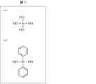
- 7 (a) and 7 (b) can be mixed during the synthesis of the conductive first polysilsesquioxane or the second polysilsesquioxane having a functional group coordinated to a quantum dot. It is a figure which shows an example of silane.
- CTTMS shown in FIG. 6 (a) which is a trialkoxysilane precursor, for example, tetraethoxysilane (TEOS), which is a raw material of silica, which is the tetraalkoxysilane shown in FIG. 7 (a), and a Si atom.
- TEOS tetraethoxysilane
- Diethoxydiphenylsilane which is a raw material for silicone, which is a dialkoxysilane having a directly bonded functional group, may be mixed with the precursor.
- polysilsesquioxane (PSQ) having a functional group containing a carbazole skeleton shown in FIG. 5 (a) is 10-5 to 10 -4 [Scm- 1].
- PSQ polysilsesquioxane
- the light-emitting device comprising a light-emitting layer containing quantum dots, in order to obtain a luminance that can be observed by the human eye, it is necessary to inject carriers in 10 -2 Acm -2 or more current density in the light emitting layer.
- an electrical conductivity required to obtain a current density 10 -2 Acm -2 in the case of 5V applied to the 50nm semiconductor layer of 10 -8 [S ⁇ cm -1] this value or more conductive If you have it, you can carry the minimum carrier transportation function.
- ⁇ in the above [Equation 1] is the reciprocal of the spread of the wave function of the hopping site.
- the distance ⁇ between hopping sites can be approximated to be proportional to the reciprocal of the cube root of the concentration C of the hopping site, and is expressed by the following [Equation 2].
- the molar ratio of the carbazole unit to the Si atom must be 20% or more in order to obtain an electric conductivity of 10-8 [S ⁇ cm -1 ] or more. is there. This value varies slightly depending on the type of pi-conjugated unit and the length of the alkyl chain, but shows the same tendency.
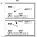
- FIG. 8A shows a case where the excited state energy of the conductive first polysilsesquioxane (conductive polysilsesquioxane) is lower than the excited state energy of the quantum dots (luminescent quantum dots). It is a figure for demonstrating the reabsorption and energy transfer which occur in FIG. 8, and (b) of FIG. 8 shows the energy of the excited state of the conductive first polysilsesquioxane (conductive polysilsesquioxane). It is a figure for demonstrating the reason why reabsorption and energy transfer do not occur when the energy is higher than the excited state energy of a quantum dot (emissive quantum dot).
- the energy of the single term excited state of the conductive first polysilsesquioxane is higher than the energy of the excited state of the quantum dots (emissive quantum dots), and Reasons why reabsorption and energy transfer do not occur when the distance between the conductive first polysilsesquioxane (conductive polysilsesquioxane) and the quantum dots (emissive quantum dots) is 1 nm or more. It is a figure for demonstrating.
- the conductive first polysilsesquioxane (conductive polysilsesquioxane) always contains the functional group R2 responsible for the conductivity, but when selecting the functional group R2 responsible for the conductivity. It is preferable to consider the following points.
- the functional group R2 responsible for conductivity is a molecule composed of a large pie-conjugated system, carrier transport by hopping conduction is easy.
- the functional group R2 responsible for conductivity has a large pi-conjugation, as shown in FIG. 8A, the energy of the quantum dots may be absorbed and the external quantum efficiency may be lowered. is there.
- the functional group R2 responsible for conductivity is arranged so that the excited state energy of the conductive polysilsesquioxane is higher than the excited state energy of the luminescent quantum dots. It is preferable to select. As shown in FIG. 8 (b), when the singlet excited state (S 1 ) level of the conductive polysilsesquioxane is higher than the excited level of the luminescent quantum dot, it is responsible for conductivity.
- the functional group R2 does not reabsorb the light emitted from the quantum dots. Further, as shown in FIG.
- the single-term excited state (S 1 ) level of the conductive polysilsesquioxane is higher than the excited level of the luminescent quantum dots, and that of the conductive polysilsesquioxane.
- the tripled excited state (T 1 ) level is lower than the excited level of the luminescent quantum dot.
- (B) in (a) and 10 in FIG. 10 is an example of a functional group R2 responsible for the conductivity, the HOMO level, LUMO level, singlet excitation level (S 1 level position) and triple It is a figure which shows the term excitation level (T 1 level).
- Figure 11 is a still another example of the functional groups R2 responsible for the conductivity, the HOMO level, LUMO level, singlet excitation level (S 1 level position) and Triplet excitation level (T 1 level It is a figure which shows the place).
- Experimental values of the singlet excited state (S 1 level position) and the triplet excitation level (T 1 level) in FIG. 10 and FIG. 11 can be obtained as follows. First polysilsesquioxane having conductivity (polysilsesquioxane having a pi-conjugated) or a functional group R2 responsible for the conductivity of the (pi-conjugated unit), singlet excitation level (S 1 level position) is , is determined from UV-Vis spectra and fluorescence spectra, triplet excitation level (T 1 level), the cryogenic (77K or less) obtained from the phosphorescence spectrum in anoxic conditions.
- the singlet excitation level (S 1 level) and the triplet excitation level (T 1 level) can also be calculated using the first-principles calculation. ..
- the calculated values shown in FIGS. 10 and 11 are structurally optimized by using the density functional theory of the Gaussian09 program package, using B3LYP for the functional and 6-31 g (d) for the base function, and the singlet excited level. (S 1 level) and triplet excitation level (T 1 level) are calculated values.
- the functional group R2 having conductivity shown in FIGS. 10 and 11 may contain, for example, an aryl group or an alkyl group.
- * is assumed to be a hydrogen atom.
- the functional group R2 responsible for each conductivity shown in FIGS. 10 and 11 includes the excitation level of the functional group R2 alone responsible for each conductivity and the functional group R2 responsible for each conductivity in polysilsesquioxane. There is almost no difference from the excitation level of.
- the energy gap between the HOMO and the LUMO is if too narrow, singlet excitation level (S 1 level position) and the triplet excitation level (T 1 level) also becomes small, FIG. As shown in (a) of 8, the energy of the quantum dots is absorbed and the external quantum efficiency is lowered.
- the functional group R2 responsible for conductivity is arranged so that the excited state energy of the conductive polysilsesquioxane is higher than the excited state energy of the luminescent quantum dots. It is preferable to select.
- the energy of the excited state of the luminescent quantum dots is different for each luminescent quantum dot having a different emission wavelength. For example, the excited state energy of a luminescent quantum dot that emits light in the green wavelength region is higher than the excited state energy of a luminescent quantum dot that emits light in the red wavelength region, and the luminescent quantum that emits light in the green wavelength region.
- the excited state energy of the luminescent quantum dots that emit light in the blue wavelength region is higher than the excited state energy of the dots.
- Conductive polysilsesquioxane sesquicarbonate considering energy of the excited state of the luminescent quantum dots that emit light in the red wavelength region silsesquioxane triplet excitation level (T 1 level) is preferably at least 1.7 eV, It is more preferably 2.2 eV or more. Further, emits light in the green wavelength region emitting triplet excitation level of the conductive polysilsesquioxane Considering the energy of the excited state of the quantum dots (T 1 level position) is not less than 2.2eV It is preferably 2.7 eV or more, and more preferably 2.7 eV or more.
- a triplet excitation conductive polysilsesquioxane Considering the energy of the excited state of the luminescent quantum dots that emit light in the blue wavelength region level (T 1 level) is not less than 2.5eV It is preferably 3.0 eV or more, and more preferably 3.0 eV or more.
- the red wavelength region emitting light-emitting quantum dots singlet excitation level of the conductive polysilsesquioxane considering the energy of the excited state (S 1 level position) is preferably at least 1.7 eV, more 2.2eV Is more preferable.
- a singlet excited conductive polysilsesquioxane Considering the energy of the excited state of the luminescent quantum dots that emit light in the green wavelength region level (S 1 level position) is not less than 2.2eV It is preferably 2.7 eV or more, and more preferably 2.7 eV or more. Further, a singlet excited conductive polysilsesquioxane Considering the energy of the excited state of the luminescent quantum dots that emit light in the blue wavelength region level (S 1 level position) is not less than 2.5eV It is preferably 3.0 eV or more, and more preferably 3.0 eV or more.
- 1,3,4-thiadiazole and oxadiazole are both the triplet excitation level (T 1 level) is not less than 2.5 eV. Further, a singlet excited state (S 1 level position) is higher than the triplet excitation level (T 1 level).
- Triazole, 1,3,4-thiadiazole and oxadiazole all have high carrier mobility because the energy gap between their HOMO and their LUMO (lowest empty level) is less than 6.0 eV.
- the functional group R2 responsible for conductivity is a carbazole skeleton, a diphenylamine skeleton, a triphenylamine skeleton, a phenoxazine skeleton, a phenothiazine skeleton, a dimethylacidine skeleton, a biphenyl skeleton, a fluorene skeleton, an imidazole skeleton, 1,2,4-triazole. It is preferably a functional group containing at least one skeleton selected from a skeleton, a 1,3,4-thiasizole skeleton, and an oxadiazole skeleton.
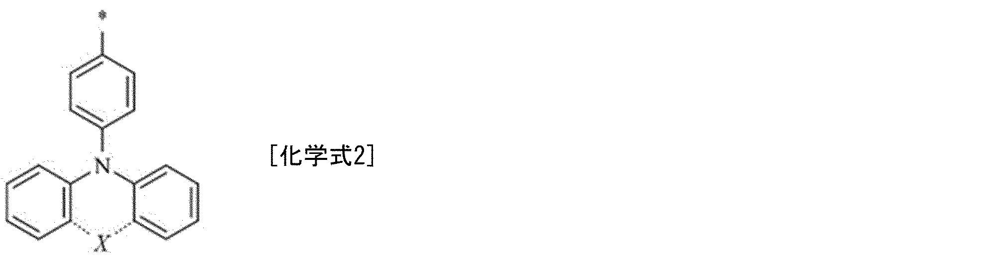
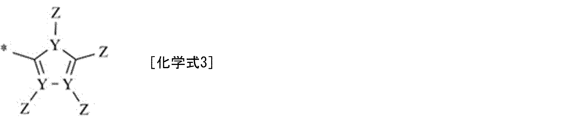
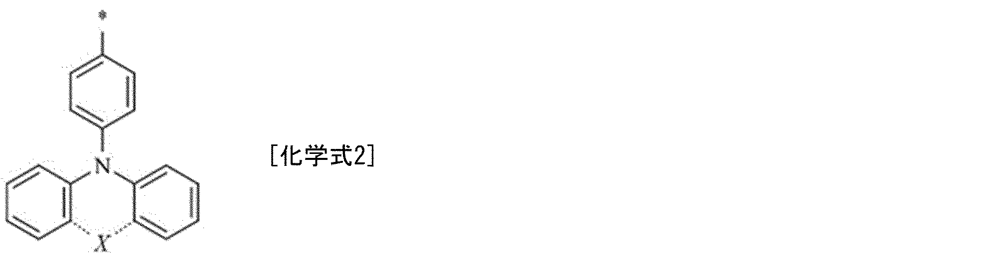
- the functional group R2 responsible for conductivity is a functional group represented by any of the following chemical formula 1, the following chemical formula 2 and the following chemical formula 3, and * in the following chemical formula 1, the following chemical formula 2 and the following chemical formula 3 is the conductivity.
- the Si atom of the main chain containing the siloxane bond of the first polysilsesquioxane having a property or the bonding portion with the side chain from the Si atom of the main chain is shown
- X in the following chemical formula 1 and the following chemical formula 2 is Indicates any atom in nitrogen atom, carbon atom, oxygen atom and sulfur atom or absence of atom
- Y in the following chemical formula 3 indicates any atom in nitrogen atom, carbon atom, oxygen atom and sulfur atom.
- Shown, Z in the following chemical formula 3 indicates any of a hydrogen atom, an aryl group and an alkyl group.
- X in the chemical formula 1 and the chemical formula 2 is any atom in the nitrogen atom, the carbon atom, the oxygen atom and the sulfur atom, and X in the chemical formula 1 and the chemical formula 2 includes a hydrogen atom and an aryl group. And any of the alkyl groups may be attached.
- a singlet excited state (S 1 level position) and from the viewpoint of the triplet excitation level (T 1 level) is used a functional group R2 responsible for the higher conductivity, triplet excitation level of Calculated It is preferable to use a functional group containing at least one skeleton selected from a carbazole skeleton, an acknowledge skeleton, a biphenyl skeleton, a diphenylamine skeleton and a triphenylamine skeleton having a position (T 1 level) of 3.18 eV or more. ..
- the ratio of the functional group R2 responsible for conductivity is preferably 20% or more, more preferably 80% or more, in terms of molar ratio with respect to the Si atom, in order to obtain a sufficient carrier transport layer. Further, if the functional group R2 responsible for conductivity is bonded to 3 out of 4 bonds of Si atom, it becomes a terminal group, so that the ratio of the functional group R2 responsible for conductivity is the Si atom. On the other hand, the molar ratio is preferably 200% or less.
- the thickness of the functional group portion 4 coordinated to the quantum dots of the first polysilsesquioxane 3 may be formed to be 1 nm or more.
- the light emitting element 20 of the present embodiment is different from the first embodiment in that the light emitting layer 23 is formed in a film shape (thin film), and the other parts are as described in the first embodiment.
- members having the same functions as the members shown in the drawings of the first embodiment are designated by the same reference numerals, and the description thereof will be omitted.
- FIG. 13A is a diagram showing a schematic configuration of the light emitting device 20 of the second embodiment
- FIG. 13B is a diagram showing a schematic configuration of nanoparticles 21 provided in the light emitting device 20 of the second embodiment. It is a figure which shows.
- a trialkoxysilane D having a functional group R1 coordinated to the quantum dot 2 (see (b) in FIG. 2) is coordinated to the quantum dot 2. Hydrolyzed under an acid / base catalyst with R1 coordinating on the surface of the quantum dots 2, that is, with the functional group R1 coordinating with the quantum dots 2 of the trialkoxysilane D molecule facing the quantum dots 2. Heat condensation is performed to form nanoparticles 21.
- nanoparticles 21 and trialkoxysilane E having a functional group R2 responsible for conductivity are added to form an acid / base catalyst.
- a film-like (thin film) light emitting layer 23 containing the first polysilsesquioxane having both of the portions 5 can be obtained.
- the light emitting layer 23 is a film (thin film) of conductive polysilsesquioxane in which quantum dots 2 are mixed.
- the functional group portion 4 coordinated to the quantum dot 2 of the conductive polysilsesquioxane and the functional group portion 5 responsible for the conductivity of the conductive polysilsesquioxane are chemically bonded.
- the light emitting layer 23 formed of a film (thin film) capable of injecting electrons and holes with a relatively small voltage to emit light and having high durability is provided.
- the light emitting element 20 can be realized.
- Embodiment 3 of the present invention will be described with reference to FIGS. 14 and 15.
- the first one having conductivity in which a functional group portion coordinating with quantum dots and a functional group portion responsible for conductivity are mixed. It differs from the first and second embodiments in that polysilsesquioxane 6 is used, and the others are as described in the first and second embodiments.
- members having the same functions as the members shown in the drawings of the first and second embodiments are designated by the same reference numerals, and the description thereof will be omitted.
- FIG. 14A is a diagram showing a schematic configuration of the light emitting device 30 of the third embodiment
- FIG. 14B is a diagram showing a schematic configuration of nanoparticles 31 provided in the light emitting device 30 of the third embodiment. It is a figure which shows.
- FIG. 15 is a diagram for explaining a method for synthesizing the first polysilsesquioxane 6 having conductivity in the light emitting layer 33 provided in the light emitting element 30 of the third embodiment.
- the quantum dots 2, the trialkoxysilane D having the functional group R1 coordinated to the quantum dots 2, and the trialkoxysilane E having the functional group R2 responsible for conductivity are added to form an acid.
- -It has conductivity in which a functional group portion coordinated to a quantum dot and a functional group portion responsible for conductivity, which are shown in FIG. 14 (b), are mixed by hydrolysis and heat condensation under a base catalyst.
- Nanoparticles 31 having a structure in which the first polysilsesquioxane 6 surrounds the quantum dots 2 can be obtained.
- the first polysilsesquioxane 6 surrounding the quantum dot 2 is formed in one step even though it has both a functional group R1 portion coordinated to the quantum dot 2 and a functional group R2 portion responsible for conductivity. be able to.
- the light emitting device 40 of the present embodiment is different from the second embodiment in that the light emitting layer 43 contains the first polysilsesquioxane 6 that can be formed in one step and is formed in a film form (thin film). , And others are as described in the second embodiment.
- members having the same functions as the members shown in the drawings of the second embodiment are designated by the same reference numerals, and the description thereof will be omitted.
- FIG. 16 is a diagram showing a schematic configuration of the light emitting element 40 of the fourth embodiment.
- the quantum dot 2, the trialkoxysilane D having the functional group R1 coordinated to the quantum dot 2 (see FIG. 15), and the trialkoxysilane E having the functional group R2 responsible for conductivity (see FIG. 15) are added.
- First polysilsesquioxane 6 having conductivity in which a functional group portion coordinated to a quantum dot and a functional group portion responsible for conductivity are mixed by hydrolysis and heat condensation under an acid / base catalyst.
- a film-like (thin film) light emitting layer 43 containing the above can be obtained. That is, the light emitting layer 43 is a film (thin film) of conductive polysilsesquioxane in which quantum dots 2 are mixed.
- a light emitting element 40 provided with a light emitting layer 43 formed in a film shape (thin film) containing the first polysilsesquioxane 6 which can be formed in one step.
- a light emitting element including a first electrode, a second electrode, and a light emitting layer provided between the first electrode and the second electrode.
- the light emitting layer is a light emitting element containing quantum dots and a first polysilsesquioxane having conductivity.
- the first functional group is a functional group represented by any of the following chemical formulas 1, the following chemical formula 2 and the following chemical formula 3.
- the following chemical formula 2 and the following chemical formula 3 indicates a bonding portion with the Si atom of the main chain or the side chain from the Si atom of the main chain.
- X in the following chemical formula 1 and the following chemical formula 2 indicates any atom in the nitrogen atom, carbon atom, oxygen atom and sulfur atom, or the absence of an atom.
- Y in the following chemical formula 3 represents any of the nitrogen atom, carbon atom, oxygen atom and sulfur atom.
- Z in the following chemical formula 3 is the light emitting device according to the second aspect, which represents any of a hydrogen atom, an aryl group and an alkyl group.
- X in the chemical formula 1 and the chemical formula 2 is any of a nitrogen atom, a carbon atom, an oxygen atom, and a sulfur atom.
- the light emitting element according to the third aspect wherein any of a hydrogen atom, an aryl group and an alkyl group is bonded to X in the chemical formula 1 and the chemical formula 2.
- the first functional group is a carbazole skeleton, a diphenylamine skeleton, a triphenylamine skeleton, a phenoxazine skeleton, a phenothiazine skeleton, a dimethylacridin skeleton, a biphenyl skeleton, a fluorene skeleton, an imidazole skeleton, 1,2,4-triazole skeleton, 1,3 , 4-The light emitting element according to aspect 2, which is a functional group containing at least one skeleton selected from a 4-thiasizole skeleton and an oxadiazole skeleton.
- the conductive first polysilsesquioxane further contains a main chain containing a siloxane bond and a second functional group coordinated to the quantum dots and bonded to the Si atom of the main chain.
- the light emitting element according to any one of aspects 1 to 7.
- the light emitting layer further contains a second polysilsesquioxane containing a main chain containing a siloxane bond and a second functional group coordinated to the quantum dots and bonded to a Si atom of the main chain.
- the light emitting element according to any one of aspects 1 to 9.
- the second functional group includes an amino group, a thiol group, an alkoxy group, a carboxy group, a phosphino group, an oxidized phosphino group, an imidazolium group, a pyridinyl group, a quaternary ammonium cation, a thiolate anion, an alkoxide anion, a carboxylate anion and a phos.
- the light emitting element according to any one of aspects 8 to 10, which is a functional group containing at least one selected from a finolato cation and an oxidized phosphinolate cation.
- the second functional group is described in any of aspects 8 to 11 in which the molar ratio is 0.1% or more and 50% or less with respect to the Si atom contained in the conductive first polysilsesquioxane. Light emitting element.
- the first polysilsesquioxane having conductivity is described in any one of aspects 1 to 12 having an electric conductivity of 10 -8 [S ⁇ cm- 1 ] or more and 10 2 [S ⁇ cm- 1 ] or less.
- Light emitting element is described in any one of aspects 1 to 12 having an electric conductivity of 10 -8 [S ⁇ cm- 1 ] or more and 10 2 [S ⁇ cm- 1 ] or less.
- the present invention can be used for a light emitting element.
Landscapes
- Chemical & Material Sciences (AREA)
- Engineering & Computer Science (AREA)
- Materials Engineering (AREA)
- Inorganic Chemistry (AREA)
- Organic Chemistry (AREA)
- Electroluminescent Light Sources (AREA)
Abstract
第1電極(11)と、第2電極(15)と、第1電極(11)と第2電極(15)との間に備えられた発光層(13)とを含む発光素子(10)であって、発光層(13)は、量子ドット(2)と、導電性を有する第1ポリシルセスキオキサン(3)とを含む。
Description
本発明は、発光素子に関する。
近年、さまざまな表示装置が開発されており、特に、QLED(Quantum dot Light Emitting Diode:量子ドット発光ダイオード)を備えた表示装置は、低消費電力化、薄型化および高画質化などを実現できる点から、高い注目を浴びている。
QLEDの分野においては、量子ドット(QD)の表面の有機の配位子が耐久性を低下させる要因となることが知られており、量子ドットを封止できる化学的・熱的に安定な材料が求められている。
図17は、量子ドットを化学的・熱的に安定な材料で封止した従来のナノ粒子及び従来のフィルムを示す図である。図17の(a)は、非特許文献1及び非特許文献2に開示されているナノ粒子100の概略構成を示す図であり、図17の(b)は、ナノ粒子100に含まれるシリカ層103を示す図である。図17の(a)に図示するように、ナノ粒子100は、量子ドット101と、量子ドット101の表面に配位したシロキサン単分子膜102と、シロキサン単分子膜102を覆うように形成されたシリカ層103とを含む。図17の(c)は、特許文献1に開示されている量子ドット111を含むフィルム110の概略構成を示す図であり、フィルム110は、量子ドット111と、量子ドット111の表面に配位するトリアルコキシシランを用いて形成したシリカ層112とを含む。図17の(d)は、特許文献2に開示されているナノ粒子120の概略構成を示す図であり、ナノ粒子120は、コアを構成するSiからなる量子ドット121と、シェルを構成するシリカ層122とを含む。
以上のように、図17に図示する従来のナノ粒子及び従来のフィルムにおいては、量子ドットを化学的・熱的に安定な材料であるシリカで封止しているので、量子ドットの耐久性を向上させることができる。
ACS Nano 2013,7,2,1472
Nanotechnology 2017,28,185603
しかしながら、非特許文献1、非特許文献2、特許文献1及び特許文献2の何れの場合においでも、量子ドットを封止する材料として、シリカが用いられている。このようなシリカ封止量子ドットは、光によって励起させて発光させることは可能であるが、シリカが大きなバンドギャップを持つ絶縁体であるため、電子や正孔を注入して発光させるためには、非常に大きな電圧が必要になるという問題がある。
本発明は、前記の問題点に鑑みてなされたものであり、比較的小さい電圧で電子や正孔を注入して発光でき、かつ、耐久性が高い発光素子を提供することを目的とする。
本発明の発光素子は、前記の課題を解決するために、第1電極と、第2電極と、前記第1電極と前記第2電極との間に備えられた発光層とを含む発光素子であって、
前記発光層は、量子ドットと、導電性を有する第1ポリシルセスキオキサンとを含む。
前記発光層は、量子ドットと、導電性を有する第1ポリシルセスキオキサンとを含む。
前記発光素子によれば、比較的小さい電圧で電子や正孔を注入して発光でき、かつ、耐久性が高い発光素子を実現できる。
本発明の一態様によれば、比較的小さい電圧で電子や正孔を注入して発光でき、かつ、耐久性が高い発光素子を提供できる。
本発明の実施の形態について図1から図16に基づいて説明すれば、次の通りである。以下、説明の便宜上、特定の実施形態にて説明した構成と同一の機能を有する構成については、同一の符号を付記し、その説明を省略する場合がある。
〔実施形態1〕
図12は、実施形態1の発光素子10の概略構成を示す図である。
図12は、実施形態1の発光素子10の概略構成を示す図である。
図12に図示するように、発光素子10は、第1電極11と、第2電極15と、第1電極11と第2電極15との間に備えられたナノ粒子1を含む発光層13とを備えている。また、発光素子10は、第1電極11と発光層13との間に第1キャリア輸送層12を、発光層13と第2電極15との間に第2キャリア輸送層14を、それぞれ備えている。
なお、発光素子10は、例えば、図示していない、薄膜トランジスタ素子(TFT素子)を複数個備えたアクティブマトリクス基板上に表示装置の解像度に応じて複数個形成され、各発光素子10に設けられた第1電極11は、前記薄膜トランジスタ素子のドレイン電極と電気的に接続されている。
本実施形態においては、前記アクティブマトリクス基板上に、第1電極11と、第1キャリア輸送層12と、発光層13と、第2キャリア輸送層14と、第2電極15とをこの順に形成した場合を一例に挙げて説明するが、これに限定されることはなく、前記アクティブマトリクス基板上に、第2電極15と、第2キャリア輸送層14と、発光層13と、第1キャリア輸送層12と、第1電極11とをこの順に形成してもよい。
発光素子10における発光層13は、第1波長領域の光を発光する。そして、前記アクティブマトリクス基板上には、第1波長領域の光を発光する発光素子10以外に、第1波長領域とはその中心波長が異なる第2波長領域の光を発光する発光層を備えた発光素子と、第1波長領域及び第2波長領域とはその中心波長が異なる第3波長領域の光を発光する発光層を備えた発光素子とが少なくとも形成されている。このような互いに異なる波長領域の光を発光する発光素子は、4種類以上形成されていてもよい。
量子ドットを含む発光層の場合、互いに発光する光の中心波長を異なるようにするためには、それぞれの発光層において、量子ドットの粒径を異なるようにしてもよく、互いに異なる種類の量子ドットを用いてもよい。
以下では、第1波長領域の光を発光する発光層13が、量子ドット2と、導電性を有する第1ポリシルセスキオキサン3とを含む場合についてのみ説明するが、第2波長領域の光を発光する発光素子の発光層及び第3波長領域の光を発光する発光素子の発光層も、同様に、量子ドットと、導電性を有する第1ポリシルセスキオキサン3とを含んでいてもよい。
発光素子10をトップエミッション型とする場合には、第1電極11としては、可視光の反射率の高い金属材料である、例えば、Al、Cu、Au、Agなどを用いることができる。また、可視光の反射率が高いのであれば、第1電極11としては、例えば、ITO(Indium Tin Oxide)とAgを含む合金とを積層して用いてもよい。第2電極15としては、可視光の透過率が高い材料(透明導電膜材料)である、例えば、ITO(Indium Tin Oxide)、IZO(Indium Zinc Oxide)、ZnO、AZO(aluminum-doped zinc oxide)、BZO(boron-doped zinc oxide)などを用いることができる。
一方、発光素子10をボトムエミッション型とする場合には、第1電極11としては、可視光の透過率が高い材料(透明導電膜材料)を用いることができ、第2電極15としては、可視光の反射率の高い金属材料または、可視光の反射率が高いのであれば、例えば、ITO(Indium Tin Oxide)とAgを含む合金とを積層して用いてもよい。
本実施形態においては、第1電極11が陽極(アノード電極)であり、第2電極15が陰極(カソード電極)である場合を一例に挙げて説明するので、第1電極11と発光層13との間の第1キャリア輸送層12は、正孔輸送層(Hole Transport Layer)であり、発光層13と第2電極15との間の第2キャリア輸送層14は、電子輸送層(Electron Transport Layer)であるが、これに限定されることはない。また、発光素子10は、第1電極11と正孔輸送層である第1キャリア輸送層12との間に正孔注入層を備えていてもよく、電子輸送層である第2キャリア輸送層14と第2電極15との間に電子注入層を備えていてもよい。さらには、正孔輸送層である第1キャリア輸送層12と発光層13との間に電子ブロッキング層を備えていてもよく、発光層13と電子輸送層である第2キャリア輸送層14との間に正孔ブロッキング層を備えていてもよい。
図1の(a)は、発光素子10の発光層13に含まれるナノ粒子1の概略構成を示す図であり、図1の(b)は、導電性を有する第1ポリシルセスキオキサン3の量子ドット2に配位する官能基部分4を示す図であり、図1の(c)は、導電性を有する第1ポリシルセスキオキサン3の概略構成を示す図である。
図1の(a)に図示するように、ナノ粒子1は、量子ドット2(蛍光体量子ドットとも称する)と、導電性を有する第1ポリシルセスキオキサン3とを含む。量子ドット2の具体的な材料としては、例えば、CdSe/CdS、CdSe/ZnS、InP/ZnS、ZnSe/ZnS、CIGS/ZnS、AgInS2/GaS及びハロゲン化鉛ペロブスカイトの何れかを用いることができ、量子ドットの粒径は3~10nm程度である。導電性を有する第1ポリシルセスキオキサン3は、量子ドット2に配位する官能基部分4と、第1ポリシルセスキオキサン3の導電性を担う官能基部分5とを含む。
図1の(b)に図示するように、導電性を有する第1ポリシルセスキオキサン3における量子ドット2に配位する官能基部分4には、量子ドット2に配位する官能基R1がある。
図1の(c)に図示するように、導電性を有する第1ポリシルセスキオキサン3は、量子ドット2に配位する官能基R1を有する量子ドット2に配位する官能基部分4と、導電性を担う官能基R2を有する第1ポリシルセスキオキサン3の導電性を担う官能基部分5との両方を有するポリシルセスキオキサンである。図1の(a)に図示するように、導電性を有する第1ポリシルセスキオキサン3は、量子ドット2を取り囲むように配置され、量子ドット2を保護する。
図2の(a)は、シリカCの合成方法を説明する図であり、図2の(b)は、量子ドット2に配位する官能基R1を有する第2ポリシルセスキオキサン4Pの合成方法を説明する図であり、図2の(c)は、導電性を有する第1ポリシルセスキオキサン3の合成方法を説明する図である。
図2の(a)に図示するように、テトラアルコキシシランA(図中R3は、例えば、メチルやエチルなどのアルキル基である)を、酸・塩基触媒下で加水分解させて、シラノール基を有するシランBを得て、シラノール基を有するシランBを加熱によって縮合させることで3次元的構造のシリカCを作製できる。シリカCは、化学的・熱的に安定な材料であるが、大きなバンドギャップを持つ絶縁体であるため、量子ドット2を保護する材料としては好ましくない。
本実施形態においては、図2の(b)に図示するように、量子ドット2に配位する官能基R1を有するトリアルコキシシランD(図中R3は、例えば、メチルやエチルなどのアルキル基である)を、量子ドット2に配位する官能基R1が量子ドット2の表面に配位した状態、すなわち、トリアルコキシシランD分子の量子ドット2に配位する官能基R1が量子ドット2を向いた状態で、酸・塩基触媒下で加水分解・加熱縮合して、量子ドット2を取り囲む3次元的構造の第2ポリシルセスキオキサン4Pの単分子膜を形成できる。
それから、図2の(c)に図示するように、さらに、導電性を担う官能基R2を有するトリアルコキシシランE(図中R3は、例えば、メチルやエチルなどのアルキル基である)を加えて、酸・塩基触媒下で加水分解・加熱縮合して、量子ドット2に配位する官能基R1を有する量子ドット2に配位する官能基部分4と、導電性を担う官能基R2を有する導電性を担う官能基部分5との両方を有する第1ポリシルセスキオキサン3を得ることができる。なお、量子ドット2に配位する官能基部分4と、導電性を担う官能基部分5とは、第2ポリシルセスキオキサン4Pのシラノール基と導電性を担う官能基R2を有するシランのシラノール基とが縮合するので、化学結合されている。
なお、量子ドット2に配位する官能基部分4と、導電性を担う官能基部分5との両方を有する第1ポリシルセスキオキサン3の合成工程においては、第1ポリシルセスキオキサン3を主に得ることができるが、第2ポリシルセスキオキサン4P、量子ドット2に配位する官能基R1を有するトリアルコキシシランD(一部がシラノール基化されたものを含む)及び導電性を担う官能基R2を有するトリアルコキシシランE(一部がシラノール基化されたものを含む)なども混在している。
ポリシルセスキオキサン(PSQ)とは、Si原子(ケイ素元素)と直接結合した官能基を有するトリアルコキシシラン(テトラアルコキシシラン、Si原子と直接結合した官能基を有するジアルコキシシラン及びSi原子と直接結合した官能基を有するモノアルコキシシランなどを含んでもよい)から生成されるSi原子と直接結合した官能基を有し、かつ、主鎖としてシロキサン結合(Si‐O‐Si)を有する高分子生成物を称する。
図3の(a)は、アミノ基を有する量子ドット2に配位する官能基R1を含むシランの一例を示す図であり、図3の(b)は、チオール基を有する量子ドット2に配位する官能基R1を含むシランの一例を示す図である。図2の(b)に図示する、量子ドット2に配位する官能基R1を有するトリアルコキシシランDとして、例えば、図3の(a)に図示する3-アミノプロピルトリエトキシシランまたは/及び図3の(b)に図示する3-(トリエトキシシリル)プロパンチオールを用いることができる。
図4の(a)、図4の(b)及び図4の(c)は、量子ドット2に配位するリガンドの一例を示す図である。
量子ドット2の材料として用いられる、例えば、CdSeなどのII-VI族またはInPなどのIII-V族の半導体量子ドット表面に配位する官能基としては、アミノ基、チオール基、アルコキシ基、カルボキシ基、ホスフィノ基、酸化ホスフィノ基、イミダゾリウム基、ピリジニル基などが知られる(Coordination Chemistry Reviews 320-321 (2016) 216‐237参照)。なお、量子ドット2に配位する官能基R1は、イオン化されて量子ドット2に配位しているものと考えられる。
図4の(a)は、量子ドット2に配位するアニオン型リガンドの一例を示している。量子ドット2に配位するアニオン型リガンドとしては、例えば、カルボキシレート、アルコキシレート、チオレート、ジチオレート、ホスフィレート、ホスフォネート、無水リン酸から選択される少なくとも1つを含むリガンドなどが挙げられる。
図4の(b)は、中性電子ドナー型リガンドの一例を示している。量子ドット2に配位する中性電子ドナー型リガンドとしては、例えば、1~3級アミン、2~3級ホスフィン、ホスフィン酸、イミダゾール、ピリジンから選択される少なくとも1つを含むリガンドなどが挙げられる。
図4の(c)は、無機リガンドの一例を示している。無機リガンドとしては、Cl-、Br-、I-、S2-、Se2-、Te2-、K+、NH4
+から少なくとも1つを選択できる。
また、図4の(a)および(b)は、シランまたはシランに結合されたアルキル基を示す。量子ドット2に配位する全てのリガンドが、直接あるいは間接的にシランに結合していなくてもよく、例えば、図4の(c)に示すような無機リガンドが配位していてもよい。
図3の(a)、図3の(b)、図4の(a)及び図4の(b)においては、量子ドット2に配位するリガンドをアルキル基(R=(CH2)n、nは1以上の自然数)を介してSi原子に取り入れているが、これに限定されることはなく、例えば、アリール基を介してSi原子に取り入れてもよく、Si原子に直接取り入れてもよい。
なお、半導体量子ドット表面に配位する官能基としてのアミノ基、チオール基、アルコキシ基、カルボキシ基、ホスフィノ基、酸化ホスフィノ基、イミダゾリウム基、ピリジニル基、第4級アンモニウムカチオン、チオラートアニオン、アルコキシドアニオン、カルボキシラートアニオン、ホスフィノラートカチオン、酸化ホスフィノラートカチオンなどの割合は、Si原子に対して、モル比で0.1%以上50%以下であることが好ましく、0.1%以上20%以下であることがさらに好ましい。50%を超えると量子ドットに配位しない余剰な配位子が存在する恐れがあるためである。
図5の(a)~図5の(h)は、導電性を担う官能基R2の一例を示す図である。官能基R2は、図5の(a)~図5の(h)に示される官能基から少なくとも1種以上選択される。
図5の(a)に図示するカルバゾール骨格を含む官能基を有するポリシルセスキオキサン(PSQ)は導電性を有することが知られている(Chem.Eur.J.2014,20,12773-12776参照)。この他にも、図5の(b)に図示するトリカルバゾール骨格を含む官能基、図5の(c)に図示するビフェニルオキシドホスフィン骨格を含む官能基、図5の(d)に図示するジフェニルアミン骨格(ビフェニルアミン骨格)を含む官能基、図5の(e)に図示するトリフェニルアミン骨格を含む官能基、図5の(f)に図示するジメチルアクリジン骨格を含む官能基、図5の(g)に図示するビフェニルトリアゾール骨格を含む官能基、図5の(h)に図示するフルオレン骨格を含む官能基、アントラセン骨格を含む官能基(図示せず)フェノキサジン骨格を含む官能基(図示せず)、フェノチアジン骨格を含む官能基(図示せず)、ビフェニル骨格を含む官能基(図示せず)、イミダゾール骨格を含む官能基(図示せず)、1,2,4-トリアゾール骨格を含む官能基(図示せず)、1,3,4-チアジアゾール骨格を含む官能基(図示せず)及びオキサジアゾール骨格を含む官能基(図示せず)などのπ共役系(パイ共役系)骨格を含む官能基を有するポリシルセスキオキサン(PSQ)は、導電性を有するポリシルセスキオキサンとして挙げることができる。
なお、図5の(a)~図5の(h)においては、導電性を担う官能基R2をアルキル基(R=(CH2)n、nは1以上の自然数)を介してSi原子に取り入れているが、これに限定されることはなく、例えば、アリール基を介してSi原子に取り入れてもよく、Si原子に直接取り入れてもよい。
図6の(a)は、導電性を担う官能基R2を含むシランの合成方法を説明する図であり、図6(b)は、図6の(a)に図示した導電性を担う官能基R2を含むシランから合成された導電性を有する第1ポリシルセスキオキサンの一例を示す図である。
導電性を担う官能基R2を含むトリアルコキシシランが入手困難な場合には、例えば、図6の(a)に図示するように、チオール基を持つシランである3-Mercaptopropyl trimethoxysilaneと、9-Vinylcarbazoleとを、光照射のみで30分間反応させ、導電性を担う官能基R2を含むトリアルコキシシランであるCarbazole-ethylthio-propyltrimethoxysilane(CTTMS)を得ることができる。このようにチオールエン反応を用いて所望の官能基を有するトリアルコキシシランを合成することが可能である(Chem.Eur.J.2014,20,12773-12776参照)。また、このようなチオールエン反応は光照射のみで進行し、副生成物を生じないため有効である。
本実施形態においては、量子ドット2に配位する官能基R1を、図2の(b)、図3の(a)及び図3の(b)に図示するような量子ドット2に配位する官能基R1を含むシランを用いて取り入れた、量子ドット2に配位する官能基部分4と、導電性を担う官能基部分5との両方を有する第1ポリシルセスキオキサン3を例に挙げて説明したが、量子ドット2に配位する官能基R1を、図2の(b)、図3の(a)及び図3の(b)に図示するような量子ドット2に配位する官能基R1を含むシランを用いて、取り入れなくてもよい。この理由は、例えば、トリアルコキシシラン前駆体である図6の(a)に図示するCarbazole-ethylthio-propyltrimethoxysilane(CTTMS)をアルコール等の溶媒中で、アルコキシ基のモル比以上の水と酸・塩基触媒下で1時間以上反応させて、加水分解した後には、多数のシラノール基(Si-OH基)が生成されるからである。したがって、シラノール基(Si-OH基)が生成されたCTTMSのシラノール基を量子ドット2に配位した状態で、60℃以上に加熱して脱水縮合すると、図6の(b)に図示する固体の導電性を担う官能基R2を有する第1ポリシルセスキオキサンが得られる。この際一部にかご状のポリシルセスキオキサンが生じるが特性上問題ない。
図7の(a)及び図7の(b)は、導電性を有する第1ポリシルセスキオキサンまたは、量子ドットに配位する官能基を有する第2ポリシルセスキオキサンの合成時に混合できるシランの一例を示す図である。
トリアルコキシシラン前駆体である図6の(a)に図示するCTTMSとともに、例えば、図7の(a)に図示するテトラアルコキシシランであるシリカの原料であるテトラエトキシシラン(TEOS)やSi原子と直接結合した官能基を有するジアルコキシシランであるシリコーンの原料であるジエトキシジフェニルシランを前駆体に混合してもよい。
Chem.Eur.J.2014,20,12773-12776によると、図5の(a)に図示するカルバゾール骨格を含む官能基を有するポリシルセスキオキサン(PSQ)は、10-5~10-4[S・cm-1]程度の電気伝導率を有する半導体であることが知られている(電気伝導率:10-8~103[S・cm-1]が半導体である)。量子ドットを含む発光層を備えた発光素子において、人の目で観測できる輝度を得るためには、発光層に10-2Acm-2以上の電流密度でキャリアを注入する必要がある。例えば、50nmの半導体層に5V印加する場合に電流密度10-2Acm-2を得るために必要な電気伝導率は10-8[S・cm-1]であり、この値以上の導電性を有していれば最低限のキャリア輸送機能を担える。
ポリシルセスキオキサンのような有機アモルファス固体がパイ共役からなるユニットを有すると、ホッピング伝導によってキャリアを輸送する。固体内でホッピング伝導が生じる際の電気伝導率σは、ホッピングサイト(ここではパイ共役ユニット)間距離γが広がるほど低下し、以下の[式1]で記述できる(有機半導体のデバイス物性,講談社,安達千波矢著参照)。


図8の(a)は、導電性を有する第1ポリシルセスキオキサン(導電性ポリシルセスキオキサン)の励起状態のエネルギーが量子ドット(発光性量子ドット)の励起状態のエネルギーより低い場合に生じる再吸収及びエネルギー移動を説明するための図であり、図8の(b)は、導電性を有する第1ポリシルセスキオキサン(導電性ポリシルセスキオキサン)の励起状態のエネルギーが量子ドット(発光性量子ドット)の励起状態のエネルギーより高い場合に再吸収及びエネルギー移動が生じない理由を説明するための図である。
図9は、導電性を有する第1ポリシルセスキオキサン(導電性ポリシルセスキオキサン)の一重項励起状態のエネルギーが量子ドット(発光性量子ドット)の励起状態のエネルギーより高く、かつ、導電性を有する第1ポリシルセスキオキサン(導電性ポリシルセスキオキサン)と量子ドット(発光性量子ドット)との間の距離が1nm以上である場合に再吸収及びエネルギー移動が生じない理由を説明するための図である。
導電性を有する第1ポリシルセスキオキサン(導電性ポリシルセスキオキサン)は、導電性を担う官能基R2を必ず含むこととなるが、この導電性を担う官能基R2を選択する際には、以下の点を考慮することが好ましい。
一般的に、導電性を担う官能基R2が大きなパイ共役からなる分子である場合、ホッピング伝導によるキャリア輸送を行いやすい。一方で、導電性を担う官能基R2が大きなパイ共役を持つ場合は、図8の(a)に図示するように、量子ドットのエネルギーを吸収して、外部量子効率を低下させてしまう場合がある。
したがって、図8の(b)に図示するように、導電性ポリシルセスキオキサンの励起状態のエネルギーが発光性量子ドットの励起状態のエネルギーより高くなるように、導電性を担う官能基R2を選択することが好ましい。図8の(b)に図示するように、導電性ポリシルセスキオキサンの一重項励起状態(S1)準位が発光性量子ドットの励起準位よりも高い場合には、導電性を担う官能基R2は量子ドットからの発光を再吸収しない。また、図8の(b)に図示するように、導電性ポリシルセスキオキサンの三重項励起状態(T1)準位が発光性量子ドットの励起準位よりも高い場合には、電子交換によって、周辺のパイ共役ユニットにエネルギー移動が生じない。
一方で、図9に図示するように、導電性ポリシルセスキオキサンの一重項励起状態(S1)準位は発光性量子ドットの励起準位よりも高く、導電性ポリシルセスキオキサンの三重項励起状態(T1)準位は発光性量子ドットの励起準位よりも低くなる、導電性を担う官能基R2を選択した場合には、発光性量子ドットと導電性を担う官能基R2を有する導電性ポリシルセスキオキサンとの間の距離を1nm以上離すことで、電子交換によって、周辺のパイ共役ユニットにエネルギー移動が生じない。
図10の(a)及び図10の(b)は、導電性を担う官能基R2の一例であって、そのHOMO準位、LUMO準位、一重項励起準位(S1準位)及び三重項励起準位(T1準位)を示す図である。
図11は、導電性を担う官能基R2のさらに他の一例であって、そのHOMO準位、LUMO準位、一重項励起準位(S1準位)及び三重項励起準位(T1準位)を示す図である。
図10及び図11における一重項励起準位(S1準位)及び三重項励起準位(T1準位)の実験値は、以下のように求めることができる。導電性を有する第1ポリシルセスキオキサン(パイ共役を有するポリシルセスキオキサン)または、導電性を担う官能基R2(パイ共役ユニット)の、一重項励起準位(S1準位)は、UV-Visスペクトルや蛍光スペクトルより求められ、三重項励起準位(T1準位)は、極低温(77K以下)無酸素条件下での燐光スペクトルから求められる。
また、図10及び図11に図示するように、一重項励起準位(S1準位)及び三重項励起準位(T1準位)は、第一原理計算を用いて計算することもできる。図10及び図11に図示する計算値は、Gaussian09プログラムパッケージの密度汎関数法により、汎関数にB3LYP、基底関数に6-31g(d)を用いて構造最適化を行い、一重項励起準位(S1準位)及び三重項励起準位(T1準位)を計算した値である。
図10及び図11に図示する分子構造中の*は、結合可能な点であり、Si原子に直接結合してもよく、例えば、アリール基やアルキル基を介してSi原子に結合してもよい。すなわち、図10及び図11に図示する導電性を担う官能基R2には、例えば、アリール基やアルキル基などが含まれてもよい。なお、ここでの第一原理計算では、*を水素原子とおいて計算を行っている。また、図10及び図11に図示する各導電性を担う官能基R2は、各導電性を担う官能基R2単体の励起準位と、ポリシルセスキオキサン内における各導電性を担う官能基R2の励起準位との差異はほぼ生じない。
一般的に、HOMO(最高被占準位)とLUMO(最低空準位)との間のエネルギーギャップが小さいほどキャリア移動度が高い。一方で、HOMOとLUMOとの間のエネルギーギャップが狭すぎる場合には、一重項励起準位(S1準位)及び三重項励起準位(T1準位)も小さくなってしまうため、図8の(a)に図示するように、量子ドットのエネルギーを吸収して、外部量子効率を低下させてしまう。
したがって、図8の(b)に図示するように、導電性ポリシルセスキオキサンの励起状態のエネルギーが発光性量子ドットの励起状態のエネルギーより高くなるように、導電性を担う官能基R2を選択することが好ましい。なお、発光性量子ドットの励起状態のエネルギーは、異なる発光波長を有する発光性量子ドットごとに異なる。例えば、赤色波長領域の光を発する発光性量子ドットの励起状態のエネルギーよりは、緑色波長領域の光を発する発光性量子ドットの励起状態のエネルギーが高く、緑色波長領域の光を発する発光性量子ドットの励起状態のエネルギーよりは、青色波長領域の光を発する発光性量子ドットの励起状態のエネルギーが高い。赤色波長領域の光を発する発光性量子ドットの励起状態のエネルギーを考慮した導電性ポリシルセスキオキサンの三重項励起準位(T1準位)は、1.7eV以上であることが好ましく、2.2eV以上であることがさらに好ましい。また、緑色波長領域の光を発する発光性量子ドットの励起状態のエネルギーを考慮した導電性ポリシルセスキオキサンの三重項励起準位(T1準位)は、2.2eV以上であることが好ましく、2.7eV以上であることがさらに好ましい。また、青色波長領域の光を発する発光性量子ドットの励起状態のエネルギーを考慮した導電性ポリシルセスキオキサンの三重項励起準位(T1準位)は、2.5eV以上であることが好ましく、3.0eV以上であることがさらに好ましい。
また、図9に図示するように、発光性量子ドットと導電性を担う官能基R2を有する導電性ポリシルセスキオキサンとの間の距離を1nm以上離すことできる場合には、赤色波長領域の光を発する発光性量子ドットの励起状態のエネルギーを考慮した導電性ポリシルセスキオキサンの一重項励起準位(S1準位)は、1.7eV以上であることが好ましく、2.2eV以上であることがさらに好ましい。また、緑色波長領域の光を発する発光性量子ドットの励起状態のエネルギーを考慮した導電性ポリシルセスキオキサンの一重項励起準位(S1準位)は、2.2eV以上であることが好ましく、2.7eV以上であることがさらに好ましい。また、青色波長領域の光を発する発光性量子ドットの励起状態のエネルギーを考慮した導電性ポリシルセスキオキサンの一重項励起準位(S1準位)は、2.5eV以上であることが好ましく、3.0eV以上であることがさらに好ましい。
図10及び図11に図示する導電性を担う官能基R2の一例である、カルバゾール、ジフェニルアミン、トリフェニルアミン、フェノキサジン、フェノチアジン、ジメチルアクリジン、ビフェニル、フルオレン、イミダゾール、1,2,4-トリアゾール、1,3,4-チアジアゾール及びオキサジアゾールは、何れもその三重項励起準位(T1準位)が2.5eV以上である。また、一重項励起準位(S1準位)は、その三重項励起準位(T1準位)よりは高い。
また、図10及び図11に図示する導電性を担う官能基R2の一例である、カルバゾール、ジフェニルアミン、トリフェニルアミン、フェノキサジン、フェノチアジン、ジメチルアクリジン、ビフェニル、フルオレン、イミダゾール、1,2,4-トリアゾール、1,3,4-チアジアゾール及びオキサジアゾールは何れも、そのHOMOとそのLUMO(最低空準位)との間のエネルギーギャップが6.0eVよりも小さいので、キャリア移動度が高い。
以上から、導電性を担う官能基R2は、カルバゾール骨格、ジフェニルアミン骨格、トリフェニルアミン骨格、フェノキサジン骨格、フェノチアジン骨格、ジメチルアクリジン骨格、ビフェニル骨格、フルオレン骨格、イミダゾール骨格、1,2,4-トリアゾール骨格、1,3,4-チアジアゾール骨格、オキサジアゾール骨格の中から選択される少なくとも1つの骨格を含む官能基であることが好ましい。
導電性を担う官能基R2は、下記化学式1、下記化学式2及び下記化学式3の何れかの構造式で示す官能基であり、下記化学式1、下記化学式2及び下記化学式3における*は、前記導電性を有する第1ポリシルセスキオキサンのシロキサン結合を含む主鎖のSi原子または、前記主鎖のSi原子からの側鎖との結合部分を示し、下記化学式1及び下記化学式2におけるXは、窒素原子、炭素原子、酸素原子及び硫黄原子中の何れかの原子または、原子不存在を示し、下記化学式3におけるYは、窒素原子、炭素原子、酸素原子及び硫黄原子中の何れかの原子を示し、下記化学式3におけるZは、水素原子、アリール基及びアルキル基中の何れかを示す。

また、一重項励起準位(S1準位)及び三重項励起準位(T1準位)がより高い導電性を担う官能基R2を用いるという観点からは、計算値としての三重項励起準位(T1準位)が3.18eV以上を示す、カルバゾール骨格、アクリジン骨格、ビフェニル骨格、ジフェニルアミン骨格及びトリフェニルアミン骨格の中から選択される少なくとも1つの骨格を含む官能基を用いることが好ましい。
導電性を担う官能基R2の割合は、十分なキャリア輸送層を得るためには、Si原子に対して、モル比で20%以上であることが好ましく、80%以上であることがさらに好ましい。また、導電性を担う官能基R2がSi原子の結合手4本のうち3本と結合してしまうと、末端基になってしまうため、導電性を担う官能基R2の割合は、Si原子に対して、モル比で200%以下であることが好ましい。
なお、本実施形態においては、図9に図示するように、導電性を有する第1ポリシルセスキオキサン3(導電性ポリシルセスキオキサン)と量子ドット2(発光性量子ドット)との間の距離を1nm以上とする必要がある場合には、第1ポリシルセスキオキサン3の量子ドットに配位する官能基部分4の厚さを1nm以上で形成すればよい。
以上のように、本実施形態によれば、比較的小さい電圧で電子や正孔を注入して発光でき、かつ、耐久性が高い発光素子10を実現できる。
〔実施形態2〕
次に、図13に基づき、本発明の実施形態2について説明する。本実施形態の発光素子20においては、発光層23が、フィルム状(薄膜)で形成されている点において、実施形態1とは異なり、その他については実施形態1において説明したとおりである。説明の便宜上、実施形態1の図面に示した部材と同じ機能を有する部材については、同じ符号を付し、その説明を省略する。
次に、図13に基づき、本発明の実施形態2について説明する。本実施形態の発光素子20においては、発光層23が、フィルム状(薄膜)で形成されている点において、実施形態1とは異なり、その他については実施形態1において説明したとおりである。説明の便宜上、実施形態1の図面に示した部材と同じ機能を有する部材については、同じ符号を付し、その説明を省略する。
図13の(a)は、実施形態2の発光素子20の概略構成を示す図であり、図13の(b)は、実施形態2の発光素子20に備えられたナノ粒子21の概略構成を示す図である。
図13の(b)に図示するように、先ず、量子ドット2に配位する官能基R1を有するトリアルコキシシランD(図2の(b)参照)を、量子ドット2に配位する官能基R1が量子ドット2の表面に配位した状態、すなわち、トリアルコキシシランD分子の量子ドット2に配位する官能基R1が量子ドット2を向いた状態で、酸・塩基触媒下で加水分解・加熱縮合して、ナノ粒子21を形成する。
そして、図13の(a)に図示するように、ナノ粒子21と、導電性を担う官能基R2を有するトリアルコキシシランE(図2の(c)参照)とを加えて、酸・塩基触媒下で加水分解・加熱縮合して、量子ドット2に配位する官能基R1を有する量子ドット2に配位する官能基部分4と、導電性を担う官能基R2を有する導電性を担う官能基部分5との両方を有する第1ポリシルセスキオキサンを含むフィルム状(薄膜)の発光層23を得ることができる。すなわち、発光層23は、量子ドット2が混在された導電性ポリシルセスキオキサンのフィルム(薄膜)である。なお、導電性ポリシルセスキオキサンの量子ドット2に配位する官能基部分4と、導電性ポリシルセスキオキサンの導電性を担う官能基部分5とは、化学結合されている。
以上のように、本実施形態によれば、比較的小さい電圧で電子や正孔を注入して発光でき、かつ、耐久性が高い、フィルム状(薄膜)で形成された発光層23を備えた発光素子20を実現できる。
〔実施形態3〕
次に、図14及び図15に基づき、本発明の実施形態3について説明する。本実施形態の発光素子30においては、発光層33に含まれるナノ粒子31において、量子ドットに配位する官能基部分と導電性を担う官能基部分とが混在している導電性を有する第1ポリシルセスキオキサン6を用いている点において実施形態1及び2とは異なり、その他については実施形態1及び2において説明したとおりである。説明の便宜上、実施形態1及び2の図面に示した部材と同じ機能を有する部材については、同じ符号を付し、その説明を省略する。
次に、図14及び図15に基づき、本発明の実施形態3について説明する。本実施形態の発光素子30においては、発光層33に含まれるナノ粒子31において、量子ドットに配位する官能基部分と導電性を担う官能基部分とが混在している導電性を有する第1ポリシルセスキオキサン6を用いている点において実施形態1及び2とは異なり、その他については実施形態1及び2において説明したとおりである。説明の便宜上、実施形態1及び2の図面に示した部材と同じ機能を有する部材については、同じ符号を付し、その説明を省略する。
図14の(a)は、実施形態3の発光素子30の概略構成を示す図であり、図14の(b)は、実施形態3の発光素子30に備えられたナノ粒子31の概略構成を示す図である。
図15は、実施形態3の発光素子30に備えられた発光層33中の導電性を有する第1ポリシルセスキオキサン6の合成方法を説明するための図である。
図15に図示するように、量子ドット2と、量子ドット2に配位する官能基R1を有するトリアルコキシシランDと、導電性を担う官能基R2を有するトリアルコキシシランEとを加えて、酸・塩基触媒下で加水分解・加熱縮合して、図14の(b)に図示する、量子ドットに配位する官能基部分と導電性を担う官能基部分とが混在している導電性を有する第1ポリシルセスキオキサン6が量子ドット2を取り囲む構造のナノ粒子31を得ることができる。
量子ドット2を取り囲む第1ポリシルセスキオキサン6は、量子ドット2に配位する官能基R1部分と導電性を担う官能基R2部分との両方を有するにも関わらず、一段階で形成することができる。
以上のように、本実施形態によれば、一段階で形成できる第1ポリシルセスキオキサン6を含む発光層33を備えた発光素子30を実現できる。
〔実施形態4〕
次に、図16に基づき、本発明の実施形態4について説明する。本実施形態の発光素子40においては、発光層43が、一段階で形成できる第1ポリシルセスキオキサン6を含み、フィルム状(薄膜)で形成されている点において、実施形態2とは異なり、その他については実施形態2において説明したとおりである。説明の便宜上、実施形態2の図面に示した部材と同じ機能を有する部材については、同じ符号を付し、その説明を省略する。
次に、図16に基づき、本発明の実施形態4について説明する。本実施形態の発光素子40においては、発光層43が、一段階で形成できる第1ポリシルセスキオキサン6を含み、フィルム状(薄膜)で形成されている点において、実施形態2とは異なり、その他については実施形態2において説明したとおりである。説明の便宜上、実施形態2の図面に示した部材と同じ機能を有する部材については、同じ符号を付し、その説明を省略する。
図16は、実施形態4の発光素子40の概略構成を示す図である。
量子ドット2と、量子ドット2に配位する官能基R1を有するトリアルコキシシランD(図15参照)と、導電性を担う官能基R2を有するトリアルコキシシランE(図15参照)とを加えて、酸・塩基触媒下で加水分解・加熱縮合して、量子ドットに配位する官能基部分と導電性を担う官能基部分とが混在している導電性を有する第1ポリシルセスキオキサン6を含むフィルム状(薄膜)の発光層43を得ることができる。すなわち、発光層43は、量子ドット2が混在された導電性ポリシルセスキオキサンのフィルム(薄膜)である。
以上のように、本実施形態によれば、一段階で形成できる第1ポリシルセスキオキサン6を含むフィルム状(薄膜)で形成された発光層43を備えた発光素子40を実現できる。
〔まとめ〕
〔態様1〕
第1電極と、第2電極と、前記第1電極と前記第2電極との間に備えられた発光層とを含む発光素子であって、
前記発光層は、量子ドットと、導電性を有する第1ポリシルセスキオキサンとを含む発光素子。
〔態様1〕
第1電極と、第2電極と、前記第1電極と前記第2電極との間に備えられた発光層とを含む発光素子であって、
前記発光層は、量子ドットと、導電性を有する第1ポリシルセスキオキサンとを含む発光素子。
〔態様2〕
前記導電性を有する第1ポリシルセスキオキサンは、シロキサン結合を含む主鎖と、前記主鎖に結合されたπ共役系骨格を含む第1官能基とを含む態様1に記載の発光素子。
前記導電性を有する第1ポリシルセスキオキサンは、シロキサン結合を含む主鎖と、前記主鎖に結合されたπ共役系骨格を含む第1官能基とを含む態様1に記載の発光素子。
〔態様3〕
前記第1官能基は、下記化学式1、下記化学式2及び下記化学式3の何れかの構造式で示す官能基であり、
下記化学式1、下記化学式2及び下記化学式3における*は、前記主鎖のSi原子または、前記主鎖のSi原子からの側鎖との結合部分を示し、
下記化学式1及び下記化学式2におけるXは、窒素原子、炭素原子、酸素原子及び硫黄原子中の何れかの原子または、原子不存在を示し、
下記化学式3におけるYは、窒素原子、炭素原子、酸素原子及び硫黄原子中の何れかの原子を示し、
下記化学式3におけるZは、水素原子、アリール基及びアルキル基中の何れかを示す態様2に記載の発光素子。

前記第1官能基は、下記化学式1、下記化学式2及び下記化学式3の何れかの構造式で示す官能基であり、
下記化学式1、下記化学式2及び下記化学式3における*は、前記主鎖のSi原子または、前記主鎖のSi原子からの側鎖との結合部分を示し、
下記化学式1及び下記化学式2におけるXは、窒素原子、炭素原子、酸素原子及び硫黄原子中の何れかの原子または、原子不存在を示し、
下記化学式3におけるYは、窒素原子、炭素原子、酸素原子及び硫黄原子中の何れかの原子を示し、
下記化学式3におけるZは、水素原子、アリール基及びアルキル基中の何れかを示す態様2に記載の発光素子。

前記化学式1及び前記化学式2におけるXは、窒素原子、炭素原子、酸素原子及び硫黄原子中の何れかの原子であり、
前記化学式1及び前記化学式2におけるXには、水素原子、アリール基及びアルキル基の何れかが結合されている態様3に記載の発光素子。
〔態様5〕
前記第1官能基は、カルバゾール骨格、アクリジン骨格、ビフェニル骨格、ジフェニルアミン骨格及びトリフェニルアミン骨格の中から選択される少なくとも1つの骨格を含む官能基である態様2に記載の発光素子。
前記第1官能基は、カルバゾール骨格、アクリジン骨格、ビフェニル骨格、ジフェニルアミン骨格及びトリフェニルアミン骨格の中から選択される少なくとも1つの骨格を含む官能基である態様2に記載の発光素子。
〔態様6〕
前記第1官能基は、カルバゾール骨格、ジフェニルアミン骨格、トリフェニルアミン骨格、フェノキサジン骨格、フェノチアジン骨格、ジメチルアクリジン骨格、ビフェニル骨格、フルオレン骨格、イミダゾール骨格、1,2,4-トリアゾール骨格、1,3,4-チアジアゾール骨格、オキサジアゾール骨格の中から選択される少なくとも1つの骨格を含む官能基である態様2に記載の発光素子。
前記第1官能基は、カルバゾール骨格、ジフェニルアミン骨格、トリフェニルアミン骨格、フェノキサジン骨格、フェノチアジン骨格、ジメチルアクリジン骨格、ビフェニル骨格、フルオレン骨格、イミダゾール骨格、1,2,4-トリアゾール骨格、1,3,4-チアジアゾール骨格、オキサジアゾール骨格の中から選択される少なくとも1つの骨格を含む官能基である態様2に記載の発光素子。
〔態様7〕
前記第1官能基は、前記導電性を有する第1ポリシルセスキオキサンに含まれるSi原子に対して、モル比で20%以上である態様2から6の何れかに記載の発光素子。
前記第1官能基は、前記導電性を有する第1ポリシルセスキオキサンに含まれるSi原子に対して、モル比で20%以上である態様2から6の何れかに記載の発光素子。
〔態様8〕
前記導電性を有する第1ポリシルセスキオキサンは、シロキサン結合を含む主鎖と、前記量子ドットに配位し、かつ、前記主鎖のSi原子に結合された第2官能基とをさらに含む態様1から7の何れかに記載の発光素子。
前記導電性を有する第1ポリシルセスキオキサンは、シロキサン結合を含む主鎖と、前記量子ドットに配位し、かつ、前記主鎖のSi原子に結合された第2官能基とをさらに含む態様1から7の何れかに記載の発光素子。
〔態様9〕
前記発光層は、前記量子ドットに配位する第2官能基を含むシランをさらに含む態様1から8の何れかに記載の発光素子。
前記発光層は、前記量子ドットに配位する第2官能基を含むシランをさらに含む態様1から8の何れかに記載の発光素子。
〔態様10〕
前記発光層は、シロキサン結合を含む主鎖と、前記量子ドットに配位し、かつ、前記主鎖のSi原子に結合された第2官能基とを含む第2ポリシルセスキオキサンをさらに含む態様1から9の何れかに記載の発光素子。
前記発光層は、シロキサン結合を含む主鎖と、前記量子ドットに配位し、かつ、前記主鎖のSi原子に結合された第2官能基とを含む第2ポリシルセスキオキサンをさらに含む態様1から9の何れかに記載の発光素子。
〔態様11〕
前記第2官能基は、アミノ基、チオール基、アルコキシ基、カルボキシ基、ホスフィノ基、酸化ホスフィノ基、イミダゾリウム基、ピリジニル基、第4級アンモニウムカチオン、チオラートアニオン、アルコキシドアニオン、カルボキシラートアニオン、ホスフィノラートカチオン、酸化ホスフィノラートカチオンの中から選択される少なくとも1種を含む官能基である態様8から10の何れかに記載の発光素子。
前記第2官能基は、アミノ基、チオール基、アルコキシ基、カルボキシ基、ホスフィノ基、酸化ホスフィノ基、イミダゾリウム基、ピリジニル基、第4級アンモニウムカチオン、チオラートアニオン、アルコキシドアニオン、カルボキシラートアニオン、ホスフィノラートカチオン、酸化ホスフィノラートカチオンの中から選択される少なくとも1種を含む官能基である態様8から10の何れかに記載の発光素子。
〔態様12〕
前記第2官能基は、前記導電性を有する第1ポリシルセスキオキサンに含まれるSi原子に対して、モル比で0.1%以上50%以下である態様8から11の何れかに記載の発光素子。
前記第2官能基は、前記導電性を有する第1ポリシルセスキオキサンに含まれるSi原子に対して、モル比で0.1%以上50%以下である態様8から11の何れかに記載の発光素子。
〔態様13〕
前記導電性を有する第1ポリシルセスキオキサンは、10-8[S・cm-1]以上102[S・cm-1]以下の電気伝導率を有する態様1から12の何れかに記載の発光素子。
前記導電性を有する第1ポリシルセスキオキサンは、10-8[S・cm-1]以上102[S・cm-1]以下の電気伝導率を有する態様1から12の何れかに記載の発光素子。
〔態様14〕
前記第1官能基の一重項励起状態のエネルギー準位は、前記量子ドットの励起状態のエネルギー準位より高い態様2に記載の発光素子。
前記第1官能基の一重項励起状態のエネルギー準位は、前記量子ドットの励起状態のエネルギー準位より高い態様2に記載の発光素子。
〔態様15〕
前記第1官能基の三重項励起状態のエネルギー準位は、前記量子ドットの励起状態のエネルギー準位より0.5eV以上高い態様2または14に記載の発光素子。
前記第1官能基の三重項励起状態のエネルギー準位は、前記量子ドットの励起状態のエネルギー準位より0.5eV以上高い態様2または14に記載の発光素子。
〔態様16〕
前記量子ドットと前記第1官能基とは、1nm以上離れている態様2または14に記載の発光素子。
前記量子ドットと前記第1官能基とは、1nm以上離れている態様2または14に記載の発光素子。
〔態様17〕
前記第1官能基のHOMO-LUMOのバンドギャップが6.0eVより小さい態様2、14、15、16の何れか1項に記載の発光素子。
前記第1官能基のHOMO-LUMOのバンドギャップが6.0eVより小さい態様2、14、15、16の何れか1項に記載の発光素子。
〔付記事項〕
本発明は上述した各実施形態に限定されるものではなく、請求項に示した範囲で種々の変更が可能であり、異なる実施形態にそれぞれ開示された技術的手段を適宜組み合わせて得られる実施形態についても本発明の技術的範囲に含まれる。さらに、各実施形態にそれぞれ開示された技術的手段を組み合わせることにより、新しい技術的特徴を形成することができる。
本発明は上述した各実施形態に限定されるものではなく、請求項に示した範囲で種々の変更が可能であり、異なる実施形態にそれぞれ開示された技術的手段を適宜組み合わせて得られる実施形態についても本発明の技術的範囲に含まれる。さらに、各実施形態にそれぞれ開示された技術的手段を組み合わせることにより、新しい技術的特徴を形成することができる。
本発明は、発光素子に利用することができる。
1、21、31 ナノ粒子
2 量子ドット
3 導電性を有する第1ポリシルセスキオキサン
4 第1ポリシルセスキオキサンの量子ドットに配位する官能基部分
4P 第2ポリシルセスキオキサン
5 第1ポリシルセスキオキサンの導電性を担う官能基部分
6 導電性を有する第1ポリシルセスキオキサン
10、20、30、40 発光素子
11 第1電極
12 第1キャリア輸送層
13、23、33、43 発光層
14 第2キャリア輸送層
15 第2電極
D 量子ドットに配位する官能基を含むシラン
E 導電性を担う官能基を含むシラン
R1 量子ドットに配位する官能基(第2官能基)
R2 導電性を担う官能基(第1官能基)
2 量子ドット
3 導電性を有する第1ポリシルセスキオキサン
4 第1ポリシルセスキオキサンの量子ドットに配位する官能基部分
4P 第2ポリシルセスキオキサン
5 第1ポリシルセスキオキサンの導電性を担う官能基部分
6 導電性を有する第1ポリシルセスキオキサン
10、20、30、40 発光素子
11 第1電極
12 第1キャリア輸送層
13、23、33、43 発光層
14 第2キャリア輸送層
15 第2電極
D 量子ドットに配位する官能基を含むシラン
E 導電性を担う官能基を含むシラン
R1 量子ドットに配位する官能基(第2官能基)
R2 導電性を担う官能基(第1官能基)
Claims (17)
- 第1電極と、第2電極と、前記第1電極と前記第2電極との間に備えられた発光層とを含む発光素子であって、
前記発光層は、量子ドットと、導電性を有する第1ポリシルセスキオキサンとを含むことを特徴とする発光素子。 - 前記導電性を有する第1ポリシルセスキオキサンは、シロキサン結合を含む主鎖と、前記主鎖に結合されたπ共役系骨格を含む第1官能基とを含むことを特徴とする請求項1に記載の発光素子。
- 前記第1官能基は、下記化学式1、下記化学式2及び下記化学式3の何れかの構造式で示す官能基であり、
下記化学式1、下記化学式2及び下記化学式3における*は、前記主鎖のSi原子または、前記主鎖のSi原子からの側鎖との結合部分を示し、
下記化学式1及び下記化学式2におけるXは、窒素原子、炭素原子、酸素原子及び硫黄原子中の何れかの原子または、原子不存在を示し、
下記化学式3におけるYは、窒素原子、炭素原子、酸素原子及び硫黄原子中の何れかの原子を示し、
下記化学式3におけるZは、水素原子、アリール基及びアルキル基中の何れかを示すことを特徴とする請求項2に記載の発光素子。

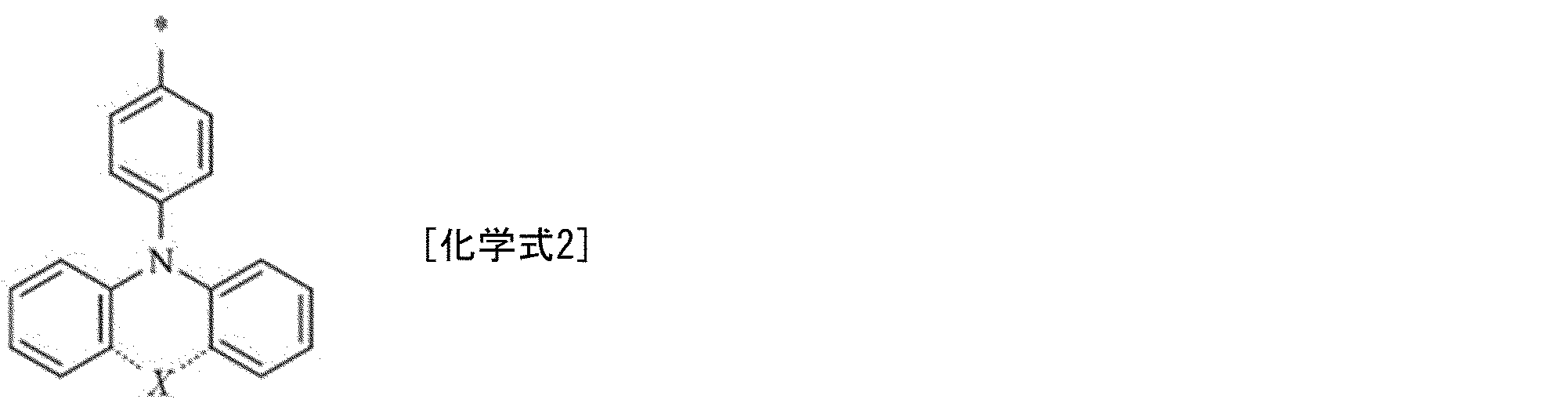
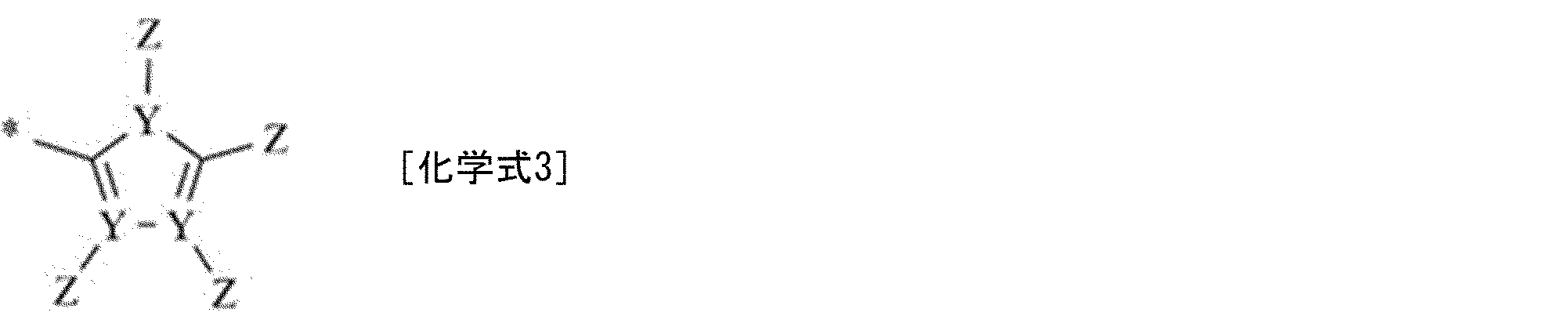
- 前記化学式1及び前記化学式2におけるXは、窒素原子、炭素原子、酸素原子及び硫黄原子中の何れかの原子であり、
前記化学式1及び前記化学式2におけるXには、水素原子、アリール基及びアルキル基の何れかが結合されていることを特徴とする請求項3に記載の発光素子。 - 前記第1官能基は、カルバゾール骨格、アクリジン骨格、ビフェニル骨格、ジフェニルアミン骨格及びトリフェニルアミン骨格の中から選択される少なくとも1つの骨格を含む官能基であることを特徴とする請求項2に記載の発光素子。
- 前記第1官能基は、カルバゾール骨格、ジフェニルアミン骨格、トリフェニルアミン骨格、フェノキサジン骨格、フェノチアジン骨格、ジメチルアクリジン骨格、ビフェニル骨格、フルオレン骨格、イミダゾール骨格、1,2,4-トリアゾール骨格、1,3,4-チアジアゾール骨格、オキサジアゾール骨格の中から選択される少なくとも1つの骨格を含む官能基であることを特徴とする請求項2に記載の発光素子。
- 前記第1官能基は、前記導電性を有する第1ポリシルセスキオキサンに含まれるSi原子に対して、モル比で20%以上であることを特徴とする請求項2から6の何れか1項に記載の発光素子。
- 前記導電性を有する第1ポリシルセスキオキサンは、シロキサン結合を含む主鎖と、前記量子ドットに配位し、かつ、前記主鎖のSi原子に結合された第2官能基とをさらに含むことを特徴とする請求項1から7の何れか1項に記載の発光素子。
- 前記発光層は、前記量子ドットに配位する第2官能基を含むシランをさらに含むことを特徴とする請求項1から8の何れか1項に記載の発光素子。
- 前記発光層は、シロキサン結合を含む主鎖と、前記量子ドットに配位し、かつ、前記主鎖のSi原子に結合された第2官能基とを含む第2ポリシルセスキオキサンをさらに含むことを特徴とする請求項1から9の何れか1項に記載の発光素子。
- 前記第2官能基は、アミノ基、チオール基、アルコキシ基、カルボキシ基、ホスフィノ基、酸化ホスフィノ基、イミダゾリウム基、ピリジニル基、第4級アンモニウムカチオン、チオラートアニオン、アルコキシドアニオン、カルボキシラートアニオン、ホスフィノラートカチオン、酸化ホスフィノラートカチオンの中から選択される少なくとも1種を含む官能基であることを特徴とする請求項8から10の何れか1項に記載の発光素子。
- 前記第2官能基は、前記導電性を有する第1ポリシルセスキオキサンに含まれるSi原子に対して、モル比で0.1%以上50%以下であることを特徴とする請求項8から11の何れか1項に記載の発光素子。
- 前記導電性を有する第1ポリシルセスキオキサンは、10-8[S・cm-1]以上102[S・cm-1]以下の電気伝導率を有することを特徴とする請求項1から12の何れか1項に記載の発光素子。
- 前記第1官能基の一重項励起状態のエネルギー準位は、前記量子ドットの励起状態のエネルギー準位より高いことを特徴とする請求項2に記載の発光素子。
- 前記第1官能基の三重項励起状態のエネルギー準位は、前記量子ドットの励起状態のエネルギー準位より0.5eV以上高いことを特徴とする請求項2または14に記載の発光素子。
- 前記量子ドットと前記第1官能基とは、1nm以上離れていることを特徴とする請求項2または14に記載の発光素子。
- 前記第1官能基のHOMO-LUMOのバンドギャップが6.0eVより小さいことを特徴とする請求項2、14、15、16の何れか1項に記載の発光素子。
Priority Applications (2)
| Application Number | Priority Date | Filing Date | Title |
|---|---|---|---|
| US17/441,067 US20220190261A1 (en) | 2019-03-22 | 2019-03-22 | Light emitting device |
| PCT/JP2019/012251 WO2020194409A1 (ja) | 2019-03-22 | 2019-03-22 | 発光素子 |
Applications Claiming Priority (1)
| Application Number | Priority Date | Filing Date | Title |
|---|---|---|---|
| PCT/JP2019/012251 WO2020194409A1 (ja) | 2019-03-22 | 2019-03-22 | 発光素子 |
Publications (1)
| Publication Number | Publication Date |
|---|---|
| WO2020194409A1 true WO2020194409A1 (ja) | 2020-10-01 |
Family
ID=72610406
Family Applications (1)
| Application Number | Title | Priority Date | Filing Date |
|---|---|---|---|
| PCT/JP2019/012251 Ceased WO2020194409A1 (ja) | 2019-03-22 | 2019-03-22 | 発光素子 |
Country Status (2)
| Country | Link |
|---|---|
| US (1) | US20220190261A1 (ja) |
| WO (1) | WO2020194409A1 (ja) |
Cited By (3)
| Publication number | Priority date | Publication date | Assignee | Title |
|---|---|---|---|---|
| WO2024201795A1 (ja) * | 2023-03-29 | 2024-10-03 | シャープディスプレイテクノロジー株式会社 | 発光素子、表示装置、および量子ドット付加体 |
| WO2024201794A1 (ja) * | 2023-03-29 | 2024-10-03 | シャープディスプレイテクノロジー株式会社 | 発光素子、表示装置、および量子ドット付加体 |
| WO2025022544A1 (ja) * | 2023-07-25 | 2025-01-30 | シャープディスプレイテクノロジー株式会社 | 発光素子、表示装置 |
Families Citing this family (1)
| Publication number | Priority date | Publication date | Assignee | Title |
|---|---|---|---|---|
| US20230313029A1 (en) * | 2020-09-18 | 2023-10-05 | Sharp Kabushiki Kaisha | Light emitting element, quantum dot-containing composition, and light emitting element manufacturing method |
Citations (4)
| Publication number | Priority date | Publication date | Assignee | Title |
|---|---|---|---|---|
| JP2009087783A (ja) * | 2007-09-28 | 2009-04-23 | Dainippon Printing Co Ltd | エレクトロルミネッセンス素子 |
| JP2013049661A (ja) * | 2011-03-16 | 2013-03-14 | Ricoh Co Ltd | カルバゾール誘導体、及び半導体ナノ結晶 |
| WO2015056749A1 (ja) * | 2013-10-17 | 2015-04-23 | 株式会社村田製作所 | ナノ粒子材料、及び発光デバイス |
| CN108832014A (zh) * | 2018-06-22 | 2018-11-16 | 南京邮电大学通达学院 | 基于CdTe/CdS量子点的发光二极管及其制备方法 |
Family Cites Families (1)
| Publication number | Priority date | Publication date | Assignee | Title |
|---|---|---|---|---|
| KR102515817B1 (ko) * | 2017-11-28 | 2023-03-29 | 엘지디스플레이 주식회사 | 발광체, 이를 포함하는 발광 필름, 발광다이오드 및 발광장치 |
-
2019
- 2019-03-22 WO PCT/JP2019/012251 patent/WO2020194409A1/ja not_active Ceased
- 2019-03-22 US US17/441,067 patent/US20220190261A1/en not_active Abandoned
Patent Citations (4)
| Publication number | Priority date | Publication date | Assignee | Title |
|---|---|---|---|---|
| JP2009087783A (ja) * | 2007-09-28 | 2009-04-23 | Dainippon Printing Co Ltd | エレクトロルミネッセンス素子 |
| JP2013049661A (ja) * | 2011-03-16 | 2013-03-14 | Ricoh Co Ltd | カルバゾール誘導体、及び半導体ナノ結晶 |
| WO2015056749A1 (ja) * | 2013-10-17 | 2015-04-23 | 株式会社村田製作所 | ナノ粒子材料、及び発光デバイス |
| CN108832014A (zh) * | 2018-06-22 | 2018-11-16 | 南京邮电大学通达学院 | 基于CdTe/CdS量子点的发光二极管及其制备方法 |
Non-Patent Citations (1)
| Title |
|---|
| SAYGILI, GAMZE ET AL.: "Enhanced electroluminescence from MEH-PPV-POSS:CulnS2 nanocomposite based organic light emitting diode", SYNTHETIC METALS, vol. 161, 13 December 2010 (2010-12-13), pages 196 - 202, XP027578947 * |
Cited By (3)
| Publication number | Priority date | Publication date | Assignee | Title |
|---|---|---|---|---|
| WO2024201795A1 (ja) * | 2023-03-29 | 2024-10-03 | シャープディスプレイテクノロジー株式会社 | 発光素子、表示装置、および量子ドット付加体 |
| WO2024201794A1 (ja) * | 2023-03-29 | 2024-10-03 | シャープディスプレイテクノロジー株式会社 | 発光素子、表示装置、および量子ドット付加体 |
| WO2025022544A1 (ja) * | 2023-07-25 | 2025-01-30 | シャープディスプレイテクノロジー株式会社 | 発光素子、表示装置 |
Also Published As
| Publication number | Publication date |
|---|---|
| US20220190261A1 (en) | 2022-06-16 |
Similar Documents
| Publication | Publication Date | Title |
|---|---|---|
| KR102712599B1 (ko) | 발광체, 이를 포함하는 발광 필름, 발광다이오드 및 발광장치 | |
| CN110021696B (zh) | 发光体以及包括其的发光膜、发光二极管和发光装置 | |
| Wu et al. | Development of InP quantum dot-based light-emitting diodes | |
| US12522565B2 (en) | Organic electroluminescent materials and devices | |
| WO2020194409A1 (ja) | 発光素子 | |
| CN107978683B (zh) | 包含n型电掺杂剂和电子传输基质的有机半导体材料以及包含该半导体材料的电子器件 | |
| US9337446B2 (en) | Encapsulated RGB OLEDs having enhanced optical output | |
| CN112313815A (zh) | 堆叠式钙钛矿发光装置 | |
| CN116076167A (zh) | 新型发光装置架构 | |
| JP2024009881A (ja) | 光子増倍材料 | |
| US20210242418A1 (en) | Pixel arrangement comprising a perovskite light emitting diode | |
| KR102535149B1 (ko) | 발광 입자, 발광 필름, 이를 포함하는 엘이디 패키지, 발광다이오드 및 및 표시장치 | |
| CN112534603A (zh) | 具有多个发射层的钙钛矿发光装置 | |
| Pan et al. | Synergistic effects of charge transport engineering and passivation enabling efficient inverted perovskite quantum-dot light-emitting diodes | |
| Kim et al. | Engineering colloidal perovskite nanocrystals and devices for efficient and large-area light-emitting diodes | |
| CN109671837B (zh) | 发光体以及包括其的发光膜、发光二极管和发光装置 | |
| Ali et al. | Control of the reaction kinetics of monodispersed InP/ZnSeS/ZnS-based quantum dots using organophosphorus compounds for electroluminescent devices | |
| Bae et al. | High-color-stability and low-driving-voltage white organic light-emitting diodes on silicon with interlayers of thin charge generation units for microdisplay applications | |
| Pei et al. | Enhancing external quantum efficiency in a sky-blue OLED by charge transfer via Si quantum dots | |
| Kim et al. | ZnSTe/ZnSe/ZnS reverse type-I blue-emitting quantum dot diodes | |
| CN113736307A (zh) | 空穴传输油墨组合物、发光装置和制备发光装置的方法 | |
| US20240431198A1 (en) | Organic electroluminescent materials and devices | |
| US20230292592A1 (en) | Organic electroluminescent materials and devices | |
| WO2025169290A1 (ja) | 発光素子、表示装置、発光素子の製造方法 | |
| WO2025169291A1 (ja) | 発光素子、表示装置、発光素子の製造方法 |
Legal Events
| Date | Code | Title | Description |
|---|---|---|---|
| 121 | Ep: the epo has been informed by wipo that ep was designated in this application |
Ref document number: 19921165 Country of ref document: EP Kind code of ref document: A1 |
|
| NENP | Non-entry into the national phase |
Ref country code: DE |
|
| 122 | Ep: pct application non-entry in european phase |
Ref document number: 19921165 Country of ref document: EP Kind code of ref document: A1 |
|
| NENP | Non-entry into the national phase |
Ref country code: JP |