WO2020153119A1 - 表示装置および表示システム - Google Patents
表示装置および表示システム Download PDFInfo
- Publication number
- WO2020153119A1 WO2020153119A1 PCT/JP2020/000201 JP2020000201W WO2020153119A1 WO 2020153119 A1 WO2020153119 A1 WO 2020153119A1 JP 2020000201 W JP2020000201 W JP 2020000201W WO 2020153119 A1 WO2020153119 A1 WO 2020153119A1
- Authority
- WO
- WIPO (PCT)
- Prior art keywords
- power generation
- display device
- power
- base material
- layer
- Prior art date
- Legal status (The legal status is an assumption and is not a legal conclusion. Google has not performed a legal analysis and makes no representation as to the accuracy of the status listed.)
- Ceased
Links
Images




Classifications
-
- G—PHYSICS
- G04—HOROLOGY
- G04G—ELECTRONIC TIME-PIECES
- G04G19/00—Electric power supply circuits specially adapted for use in electronic time-pieces
-
- G—PHYSICS
- G09—EDUCATION; CRYPTOGRAPHY; DISPLAY; ADVERTISING; SEALS
- G09F—DISPLAYING; ADVERTISING; SIGNS; LABELS OR NAME-PLATES; SEALS
- G09F9/00—Indicating arrangements for variable information in which the information is built-up on a support by selection or combination of individual elements
-
- G—PHYSICS
- G09—EDUCATION; CRYPTOGRAPHY; DISPLAY; ADVERTISING; SEALS
- G09F—DISPLAYING; ADVERTISING; SIGNS; LABELS OR NAME-PLATES; SEALS
- G09F9/00—Indicating arrangements for variable information in which the information is built-up on a support by selection or combination of individual elements
- G09F9/30—Indicating arrangements for variable information in which the information is built-up on a support by selection or combination of individual elements in which the desired character or characters are formed by combining individual elements
-
- H—ELECTRICITY
- H02—GENERATION; CONVERSION OR DISTRIBUTION OF ELECTRIC POWER
- H02N—ELECTRIC MACHINES NOT OTHERWISE PROVIDED FOR
- H02N11/00—Generators or motors not provided for elsewhere; Alleged perpetua mobilia obtained by electric or magnetic means
Definitions
- the present invention relates to a display device and a display system.
- Liquid crystal display devices, organic electroluminescence display devices, etc. are used as display devices for mobile electronic devices such as mobile phones and personal digital assistants.
- a display device such as a portable electronic device
- electric power or voltage for driving the display device is supplied from a power supply device (for example, a battery) provided separately from the display device.
- a power supply device for example, a battery
- Patent Document 1 discloses a wristwatch device having a function of generating power by a solar cell, a temperature difference, or rotational movement of a rotor, and a time display unit.
- the wristwatch device is driven using electric power or voltage generated by power generation. Further, the wristwatch device has a function of displaying an abnormality such as the power generation status, the electric capacity, or the stop of the time display unit.
- One of the objects of the present invention is to provide a display device and a display system having a built-in power generation unit.
- a reflective display device comprising: a power generation layer portion including a power generation element; and a display portion including a plurality of pixels and an insulating layer, wherein the insulating layer is a first surface and a second surface on a side opposite to the first surface. A surface, the plurality of pixels are provided on the first surface, and the power generation unit is in contact with the second surface.
- a power generation unit including a power generation element, a display unit including a plurality of pixels and an insulating layer, a display system electrically connected to the power generation unit and the display unit, and generated by the power generation unit from the power generation unit to the display unit.
- a control device for controlling supply of electromotive force the insulating layer has a first surface and a second surface opposite to the first surface, and the plurality of pixels are provided on the first surface, The power generation unit contacts the second surface.
- the first base material described in this specification has at least one planar main surface, and each layer such as an insulating layer, a semiconductor layer, and a conductive layer, or each element such as a transistor and a light emitting element is provided on the one main surface. Shall be provided.
- the display device according to the embodiment of the present invention is, for example, a liquid crystal display device.
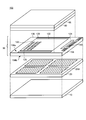
- FIG. 1 is a schematic perspective view showing a configuration of a display device according to an embodiment of the present invention.
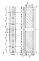
- FIG. 2 is a schematic cross-sectional view showing the configuration of the display device 100 according to the embodiment of the present invention.
- FIG. 3 is a schematic plan view of the display system 200 according to the embodiment of the present invention. 2 is a cross-sectional view showing a cross section taken along a partial region of FIG. 1, and FIG. 2 is also a cross-sectional view showing a cross section taken along A1-A2 of a B region shown in FIG.
- the display device 100 includes a first base material 10, a power generation layer 20, an array layer 30, a second base material 90, and a polarizing plate 95.
- the power generation layer 20 is provided on the first base material 10.
- the array layer 30 is provided so as to contact the power generation layer 20.
- the polarizing plate 95 is provided on the second base material 90.
- the power generation layer 20 includes a power generation element 250, which will be described in detail later.
- the power generation element 250 is, for example, a thermoelectric element (also called a thermoelectric conversion element).
- the thermoelectric element includes an n-type semiconductor portion and a p-type semiconductor portion.
- the n-type semiconductor portion and the p-type semiconductor portion are electrically connected.
- the n-type semiconductor portion is formed of an n-type semiconductor material
- the p-type semiconductor portion is formed of a p-type semiconductor material.
- the display device 100 can generate electric power by incorporating the power generation element 250. Although the details will be described later, the generated power is stored by the display system 200 described later, and the display system 200 can use the power for driving the display device 100.
- the display device 100 illustrated in FIG. 1 includes four power generating elements 250, but the configuration including the number and size of the power generating elements 250 is not limited to this example. Further, although an example including the n-type semiconductor portion and the p-type semiconductor portion is shown as an example of the configuration of the power generation element 250, the configuration of the power generation element 250 is not limited to the example shown here.
- the power generation element 250 may have a configuration in which two members containing different kinds of metals as materials are connected to each other.
- the power generation element 250 may have any configuration as long as it can generate power, voltage, or the like by being given heat. Further, the configuration of the power generation element 250 may be appropriately determined depending on the use or specifications of the display device 100 without departing from the configuration of the present invention. Note that in this specification and the like, the generated power may be referred to as an electromotive force.
- the array layer 30 has a base layer 138, an image signal line driving circuit 124, a scanning signal line driving circuit 126, a scanning signal line driving circuit 128, a terminal electrode 140, and a peripheral region 136.
- the image signal line driver circuit 124, the scanning signal line driver circuit 126, the scanning signal line driver circuit 128, the terminal electrode 140, and the peripheral region 136 are provided over the base layer 138.
- the display unit 122 is illustrated in a plan view so as to make the drawing easy to see.
- the display unit 122 has a plurality of pixels 120 for displaying an image on the display device 100, and in reality, the array layer 30, the first alignment film 40, the liquid crystal layer 50, the second alignment film 60, and the second electrode layer 70. , The color filter layer 80, and a part of the second base material 90.
- the display unit 122 is provided so as to be in contact with the power generation layer 20.
- the underlayer 138 has a first surface 138a and a second surface 138b.
- the second surface 138b is a surface opposite to the first surface 138a by approximately 180 degrees, that is, the second surface 138b is a surface opposite to the first surface 138a.
- the first surface 138a contacts the insulating layer 36.
- the second surface 138b contacts the power generation layer 20.
- the base layer 138 is an insulating layer.
- the material forming the base layer 138 is a material containing an inorganic compound such as silicon oxide, silicon nitride oxide, silicon oxynitride, silicon nitride, or aluminum oxide.
- the underlayer 138 is formed by one layer, but is not limited to this example.
- the base layer 138 may have a structure in which layers formed of a material containing a plurality of inorganic compounds are stacked.
- the base layer 138 may be formed by stacking a layer formed of silicon oxide and a layer formed of silicon nitride.
- the material forming the underlayer 138 may be an organic insulating material.
- the base layer 138 may have a structure in which a layer formed of a material containing an inorganic compound and a layer formed of an organic insulating material are stacked. It may be appropriately selected in consideration of adhesion to layers included in the power generation layer 20 and the array layer 30, diffusion of impurities, and penetration of impurities.
- the first alignment film 40, the liquid crystal layer 50, the second alignment film 60, the second electrode layer 70, and the color filter layer 80 form the array layer 30 and the second base material 90. It is provided between.
- the array layer 30 includes a first electrode layer 34 having a plurality of first electrodes formed thereon and an insulating layer 36 having an insulating film formed thereon.
- the first alignment film 40 is provided on the array layer 30.
- the first alignment film 40 has a role of insulating the first electrode layer 34 and the second electrode layer 70 provided on the side facing the liquid crystal layer 50.
- the facing substrate provided so as to face the upper surface of the first base material 10 will be described with reference to FIG.
- the opposite substrate has, for example, a second alignment film 60, a second electrode layer 70, a color filter layer 80, a second base material 90, and a polarizing plate 95.
- a polarizing plate 95 is provided on the second base material 90.
- the color filter layer 80 is provided below the second base material 90.
- the color filter layer 80 includes a red color filter layer 82, a green color filter layer 84, and a blue color filter layer 86.
- the light shielding layer 88 may be provided between the color filter layers.
- the second electrode layer 70 is provided below the color filter layer 80.
- the second electrode layer 70 includes a plurality of second electrodes 72.
- the pixel 120 includes one first electrode 32 and one second electrode 72 facing the one first electrode 32.
- the display device 100 is manufactured by bonding the opposite substrate and the substrate in which the first alignment film 40 is provided on the first base material 10 to each other.
- the opposite substrate and the substrate having the first alignment film 40 provided on the first base material 10 can be attached to each other by using a sealing material or the like.
- the liquid crystal layer 50 is provided between the counter substrate and the substrate in which the first alignment film 40 is provided on the first base material 10.
- the first base material 10 and the second base material may have flexibility.
- the display device 100 has flexibility because the first base material 10 and the second base material have flexibility. Therefore, the display device 100 can be used as a wearable device attached to a curved surface such as a human body.
- the material used for the first base material 10 and the second base material is, for example, polyimide.
- the display device 100 may be a passive display device or an active display device.
- the array layer 30 includes at least a first electrode layer 34 having a plurality of first electrodes 32 formed thereon and an insulating layer 36 having an insulating film formed thereon.
- the second electrode layer 70 includes a plurality of second electrodes 72.
- the pixel 120 includes one first electrode 32 and one second electrode 72 facing the one first electrode 32.
- the display device 100 may display an image by applying a voltage to each of the one first electrode 32 and the one second electrode 72 facing the one first electrode 32.
- the second electrode layer 70 may include an insulating layer for insulating adjacent second electrodes.
- the array layer 30 includes a plurality of thin film transistors (TFTs) and a plurality of capacitive elements.
- the pixel 120 includes one first electrode 32 electrically connected to one TFT and one second electrode 72 facing the one first electrode 32.
- the display device 100 may display an image by applying a voltage to each of the one first electrode 32 and the one second electrode 72 facing the one first electrode 32.
- the TFT includes, for example, a semiconductor layer, a gate insulating film, a gate electrode, an interlayer film, and a source/drain electrode.
- TFTs As a method of forming a TFT, a structure of a thin film transistor or a capacitor, respective films, layers, and materials of respective portions, known techniques usually used in the technical field of the present invention can be adopted. Therefore, the description of the method for manufacturing the TFT is omitted in this specification.
- the display device 100 may be a transmissive display device, a reflective display device, or a semi-transmissive display device.
- a backlight is not required, so that it is possible to reduce the weight of the display device 100, reduce the power consumption, and reduce the manufacturing cost.
- the structure of the pixel may be a structure corresponding to the IPS mode or a structure corresponding to the VA mode.
- the structure of the pixel may be any structure that allows the display system 200 to display an image.
- a backlight is arranged on the side of the display device 100 where the power generation element 250 is provided, and an image is displayed by the power generated by the power generation element 250 due to the heat of the backlight. It can be displayed on the device 300.
- the display device 100 is attached to a window glass or a windshield of a car, sunlight hits the window glass or the windshield of the car, and an image is displayed on the display device 100 by the power generated by the power generation element 250 by the heat of the sunlight. can do.
- the method for manufacturing a display device according to the embodiment of the present invention can use a photolithography technique generally used in manufacturing a display device, unless otherwise specified. Further, the manufacturing method used in the technical field of the present invention can be adopted as the manufacturing method of the display device according to the embodiment of the present invention. As in the manufacture of the TFT, the materials of the respective films, layers, and respective portions can employ known techniques usually used in the technical field of the present invention. Therefore, in this specification, the description of the method for manufacturing the display device is omitted.
- the display device 100 is a passive display device.
- a plurality of pixels 120 are provided on the display unit 122.
- the scanning signal line drive circuit 126 (the scanning signal line drive circuit 128 is omitted) and the image signal line drive circuit 124 are provided in the peripheral region 136.
- the scan signal line driver circuit 126 and the image signal line driver circuit 124 control driving of the pixels 120.
- the scanning signal line drive circuit 126 and the image signal line drive circuit 124 show an example using an IC chip.
- FIG. 2 shows an example in which the scanning signal line drive circuit 126 and the image signal line drive circuit 124 are provided on the first base material 10, the present invention is not limited to this example.
- a drive circuit formed on a substrate (semiconductor substrate or the like) different from the first base material 10 is mounted on a connector 214 such as the first base material 10 or a flexible printed circuit (FPC) board. It may be provided.
- part or all of the circuits included in the scan signal line driver circuit 126 and the image signal line driver circuit 124 are formed over a substrate different from the first base material 10 and formed over the first base material 10 or the connector 214. It may be provided.
- the drive circuit included in the scan signal line drive circuit 126 or a part of the drive circuit may be directly formed on the first base material 10.
- display elements such as liquid crystal elements provided in the pixels 120 and various semiconductor elements for controlling them are formed on the first base material 10.
- the display system 200 includes the first wiring 206, the contact hole 208, the first terminal wiring 210, the first terminal 212, the second wiring 216, the contact hole 218, the second terminal wiring 220, and the second wiring. It also has terminals 222 and the like. These are also provided on the first base material 10.
- the power generating element 250 is electrically connected to the first wiring 206 extending from the peripheral area 136.
- the first wiring 206 extends in the peripheral region 136 and is electrically connected to the first terminal wiring 210 through the contact hole 208.
- the first terminal wiring 210 is exposed near the end portion of the display device 100 and forms the first terminal 212.
- the first terminal 212 is connected to the connector 214.
- the electric power generated by the power generation element 250 can be supplied to the control device 400 via the connector 214.
- the electric power supplied to control device 400 is stored in power storage unit 14 of control device 400.
- the display device 100 can be driven by the power.
- a signal or power supply for driving the pixel 120 may be supplied to the pixel 120 from the control device 400 via the second wiring 216 extending from the peripheral region 136.
- the pixel 120 is electrically connected to the second wiring 216 extending from the peripheral region 136.
- the second wiring 216 extends in the peripheral region 136 and is electrically connected to the second terminal wiring 220 via the contact hole 218.
- the second terminal wiring 220 is exposed near the end portion of the display device 100 to form the second terminal 222.
- the second terminal 222 is connected to the connector 214.
- a signal or power supply for driving the pixel 120 is supplied to the pixel 120 from the control device 400 through the first terminal 212 or the second terminal 222, the scan signal line driver circuit 126, and the image signal line driver circuit 124.
- the first terminal 212 or the second terminal 222 can be formed so as to be aligned with one side of the display device 100. Therefore, by using the single connector 214, it is possible to independently supply a voltage or a signal to each of the display unit 122, the scanning signal line drive circuit 126, and the image signal line drive circuit 124.
- FIG. 2 shows an example in which the array of pixels 120 is a stripe array.
- Each of the pixels 120 may correspond to, for example, three subpixels 130, 132, and 134.
- One pixel may be formed by three sub-pixels.
- Each sub-pixel is provided with one display element such as a liquid crystal element.
- the color to which the sub pixel corresponds is determined by the characteristics of the liquid crystal element or the color filter provided on the sub pixel.
- each of the pixels 120 includes a liquid crystal element is shown.
- the pixel 120 is a minimum unit that constitutes a part of the image reproduced on the display unit 122.
- the sub pixel included in the display portion 122 is included in any of the pixels.
- the three subpixels 130, 132, and 134 can be configured to give different colors.
- each of the sub-pixel 130, the sub-pixel 132, and the sub-pixel 134 can be provided with a color filter layer that emits three primary colors of red, green, and blue. Then, by supplying an arbitrary voltage or current to each of the three subpixels, a full-color display device can be provided.
- the control device 400 includes at least the power storage unit 14, the signal supply circuit 16, and the power supply circuit 22. Further, the control device 400 is electrically connected to the external power supply device 410 via the connector 224.
- the signal supply circuit 16 can generate a video signal and a signal for driving the display device 100.
- the signal supply circuit 16 can generate one or more signals. Further, the generated signals may be a plurality of the same signals, a plurality of different signals, or the same signal and a plurality of different signals.
- the signal generated by the signal supply circuit 16 may be appropriately selected without departing from the configuration of the present invention.
- the generated signal is supplied to each of the display unit 122, the scanning signal line drive circuit 126, and the image signal line drive circuit 124.
- the power storage unit 14 can store the electric power generated by the power generation element 250.
- the power storage unit includes, for example, an electric field capacitor or a ceramic capacitor. Further, the display device 100 can be driven by the power.
- the display system 200 does not have to include the power storage unit 14. Since the display system 200 does not include the power storage unit 14, the power generated by the power generation element 250 can be directly supplied to the power supply circuit 22 described below without storing the power. Therefore, since the display system 200 does not include the power storage unit 14, the manufacturing cost of the display system 200 can be suppressed.
- the power supply circuit 22 supplies power to the signal supply circuit 16 and the display device 100.
- the power supply circuit 22 can generate a voltage corresponding to a power supply supplied to the display device 100, the scanning signal line drive circuit 126, and the image signal line drive circuit 124 based on the electric power stored in the power storage unit 14.
- the power supply circuit 22 includes, for example, a DC-DC conversion circuit and a charge pump circuit.
- the external power supply device 410 Like the power supply circuit 22, the external power supply device 410 generates a voltage corresponding to the power supply supplied to the scanning signal line drive circuit 126 and the image signal line drive circuit 124, and supplies power to the signal supply circuit 16 and the display device 100. Can be supplied.
- the external power supply device 410 does not have to supply the display device 100 with electric power.
- the display system 200 may not include the external power supply device 410. Therefore, the display system 200 can suppress the manufacturing cost of the display system 200 by not including the external power supply device 410.
- the FPC can be used for the connector 224 as well.
- the connector 214 also has a role of supplying a video signal, a timing signal for controlling the operation of the circuit, a power supply, and the like to the display device 100, the scan signal line driver circuit 126, and the image signal line driver circuit 124.
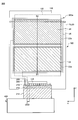
- FIG. 4 is a plan view showing the configuration of the power generation layer 20 according to the first embodiment. Except for the configuration related to the power generation layer 20 and the connection of the power generation layer 20 and the connector 214, the configuration is the same as or similar to those in FIGS. 1 to 3, and thus the description thereof is omitted here. 4, the connector 224, the external power supply device 410, the pixel 120, the base layer 138, and the like shown in FIG. 3 are omitted in FIG. Note that in this specification and the like, the power generation layer may be referred to as a power generation unit.
- the power generation layer 20 includes a power generation element 250a.
- the power generation element 250a includes a first wiring electrode 22a, a first wiring electrode 22b, a p-type semiconductor section 24, a second wiring electrode 26, and an n-type semiconductor section 28.
- the first wiring electrode 22a is electrically connected to the first wiring 206.
- the first terminal of the p-type semiconductor portion 24 is electrically connected to the first wiring electrode 22a.
- the second terminal of the p-type semiconductor portion 24 is electrically connected to the second wiring electrode 26.
- the first terminal of the n-type semiconductor portion 28 is electrically connected to the second wiring electrode 26.
- the second terminal of the n-type semiconductor portion 28 is electrically connected to the first wiring electrode 22b.
- the first wiring electrode 22b is electrically connected to the first wiring 206.
- a material for forming the first wiring electrode 22a and the first wiring electrode 22b a material having a high thermal conductivity such as copper, aluminum, or silver may be used.
- a material for forming the second wiring electrode 26 the same material as the first wiring electrode 22a and the first wiring electrode 22b may be used.
- a material for forming the p-type semiconductor portion 24 for example, a material having a high electric conductivity such as PbTeSe or SiGe to which a p-type carrier is added may be used.
- the material forming the n-type semiconductor portion 28 may be a material having a high electric conductivity, such as PbTeSe or SiGe to which an n-type carrier is added.
- the semiconductor portion forming the power generation element may be referred to as a power generation member.
- the power generation element 250 may have a configuration in which two members containing different kinds of metals as materials are connected to each other.
- materials of different kinds of metals for example, materials having high electric conductivity such as potassium, aluminum and copper may be used.
- the heat generated by the power generating element 250a causes a potential difference between the first wiring electrode 22a and the first wiring electrode 22b.
- a temperature difference occurs between the second wiring electrode 26 and the first wiring electrode 22a and the first wiring electrode 22b.
- a potential difference is generated between the wiring electrode 22b and the wiring electrode 22b. Therefore, the power generation element 250a can generate electric power.
- thermoelectric performance index Z[1/K] The performance of the power generation element 250a (thermoelectric element) can be represented by the thermoelectric performance index Z[1/K] of the following mathematical expression (2).
- S is the Seebeck coefficient
- ⁇ is the electrical conductivity
- ⁇ is the thermal conductivity.
- FIG. 4 shows an example in which the power generation element 250a is provided on a part of the upper surface of the first base material 10, but the present invention is not limited to this example.
- the power generation element 250a may be provided on the entire surface of the first base material 10. As the area of the power generation element 250a increases, the electrical conductivity of the power generation element 250a improves, so that the thermoelectric figure of merit Z shown in Formula (2) can be increased. That is, the power generation efficiency can be improved by increasing the area of the power generation element 250a.
- the first wiring electrode 22a is electrically connected to the GND terminal in the display system 200 via the first wiring 206, the contact hole 208, the first terminal wiring 210, the first terminal 212, and the connector 214. You may.
- the image signal line drive circuit 124 is also electrically connected to the GND terminal. Therefore, the image signal line drive circuit 124 and the first wiring electrode 22a can share the GND terminal. Although not shown, the image signal line driving circuit 124, the first wiring electrode 22a, and the scanning signal line driving circuit 126 can share the GND terminal. By sharing the GND terminal in each circuit or each part in the display system 200, the number of terminals can be reduced, so that the manufacturing cost of the display device 100 can be reduced.
- each circuit or each part is supplied with the GND potential from the same GND terminal.
- the reference potential can be made uniform by making the GND potential uniform in each circuit or each part.
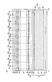
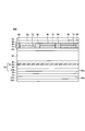
- FIG. 5 is a cross-sectional view showing the configuration of the power generation layer 20 according to the first embodiment, which is a cross-sectional view taken along line B1-B2 of FIG.
- the cross section along B1-B2 in FIG. 4 is a plane parallel or substantially parallel to the Y direction of the display device 100.
- the power generating element 250a includes a first wiring electrode 22a, a first wiring electrode 22b, a p-type semiconductor section 24, a second wiring electrode 26, and an n-type semiconductor section 28.
- the first terminal 24-1 of the p-type semiconductor portion 24 is electrically connected to the first wiring electrode 22a.
- the second terminal 24-2 of the p-type semiconductor portion 24 is electrically connected to the second wiring electrode 26.
- the first terminal 28-1 of the n-type semiconductor portion 28 is electrically connected to the second wiring electrode 26.
- the second terminal 28-2 of the n-type semiconductor portion 28 is electrically connected to the first wiring electrode 22b.
- the insulating film 27 is provided between the p-type semiconductor portion 24 and the n-type semiconductor portion 28.
- the p-type semiconductor section 24 and the n-type semiconductor section 28 are surrounded by the insulating film 27.
- the insulating film 27 is also provided between the first wiring electrode 22a and the first wiring electrode 22b. That is, the p-type semiconductor portion 24 and the n-type semiconductor portion 28 are provided on the first base material 10 so as to be separated from each other, electrically connected by the second wiring electrode 26, and insulated by the insulating film 27. There is. Although not shown, part of the insulating film 27 is provided in the peripheral region 136 so as to be in contact with the first base material 10. Note that in this specification and the like, the insulating film 27 may be referred to as an insulating member.
- Each of the eight pixels 120 provided in the Y direction of the display device 100 includes a first electrode 32 and a second electrode 72 facing the first electrode 32.
- FIG. 6 is a cross-sectional view showing the configuration of the power generation layer 20 according to the first embodiment, which is a cross-sectional view taken along the line C1-C2 of FIG.
- the cross section along C1-C2 in FIG. 4 is a plane parallel or substantially parallel to the X direction of the display device 100.
- the power generation element 250a includes a first wiring electrode 22b, a second wiring electrode 26, and an n-type semiconductor section 28.
- the first terminal 28-1 of the n-type semiconductor portion 28 is electrically connected to the second wiring electrode 26.
- the second terminal 28-2 of the n-type semiconductor portion 28 is electrically connected to the first wiring electrode 22b.
- the insulating film 27 is provided so as to surround the n-type semiconductor portion 28. Although not shown, the insulating film 27 is provided so as to surround the p-type semiconductor portion 24 as well as the n-type semiconductor portion 28.
- Each of the nine pixels 120 provided in the X direction of the display device 100 includes a first electrode 32 and a second electrode 72 facing the first electrode 32.
- the first electrode 32 is shared by the nine pixels 120.
- the power generation element 250a is provided below the display unit 122 so as to overlap with the display unit 122. Further, as shown in FIGS. 5 and 6, the power generation element 250 a is provided below the plurality of pixels 120 so as to overlap the plurality of pixels 120. Since the power generation element 250a overlaps with the plurality of pixels 120, heat generated when driving the plurality of pixels 120 can generate larger electric power.
- the power generation layer 20 can utilize the photolithography technology generally used in the manufacture of display devices.
- the power generation layer 20 may be formed using, for example, a liquid crystal dropping device, an inkjet printer, or a screen printer. Further, the power generation layer 20 may be formed using electroplating.
- the power generation layer 20 is formed by the manufacturing method used in the technical field of the present invention. Therefore, in the array layer including the power generation layer 20 and the display portion, as in the manufacture of the TFT, the material of each film, layer, and each portion adopts a known technique usually used in the technical field of the present invention. You can Therefore, in this specification, detailed description of the method for manufacturing the power generation layer 20 is omitted.
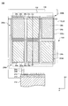
- FIG. 7 is a plan view showing the configuration of the power generation layer 20 according to the first embodiment.
- the power generation layer 20 includes a power generation element 250a, a power generation element 250b, and a power generation element 250c.
- the power generation layer 20 has the same or similar configuration as that of FIG. 4 except that it has three power generating elements 250, and therefore the description thereof is omitted here. Further, the same or similar configurations as those in FIGS. 1 to 3, 5 and 6 may be omitted.
- the power generation layer 20 includes a power generation element 250a, a power generation element 250b, and a power generation element 250c.
- the power generation element 250a includes a first wiring electrode 22a, a first wiring electrode 22ab, a p-type semiconductor portion 24a, a second wiring electrode 26a, and an n-type semiconductor portion 28a.
- the power generation element 250b includes a first wiring electrode 22ab, a first wiring electrode 22bc, a p-type semiconductor portion 24b, a second wiring electrode 26b, and an n-type semiconductor portion 28b.
- the power generation element 250c includes a first wiring electrode 22bc, a first wiring electrode 22c, a p-type semiconductor portion 24c, a second wiring electrode 26c, and an n-type semiconductor portion 28c. Note that the materials described in FIG. 4 can be used as the materials for forming the power generation element 250a, the power generation element 250b, and the power generation element 250c.
- the first wiring electrode 22a is electrically connected to the first wiring 206.
- the first terminal of the p-type semiconductor portion 24a is electrically connected to the first wiring electrode 22a.
- the second terminal of the p-type semiconductor portion 24a is electrically connected to the second wiring electrode 26a.
- the first terminal of the n-type semiconductor portion 28a is electrically connected to the second wiring electrode 26a.
- the second terminal of the n-type semiconductor portion 28a is electrically connected to the first wiring electrode 22ab.
- the first terminal of the p-type semiconductor portion 24b is electrically connected to the first wiring electrode 22ab.
- the second terminal of the p-type semiconductor portion 24b is electrically connected to the second wiring electrode 26b.
- the first terminal of the n-type semiconductor portion 28b is electrically connected to the second wiring electrode 26b.
- the second terminal of the n-type semiconductor portion 28b is electrically connected to the first wiring electrode 22bc.
- the first terminal of the p-type semiconductor portion 24c is electrically connected to the first wiring electrode 22bc.
- the second terminal of the p-type semiconductor portion 24c is electrically connected to the second wiring electrode 26c.
- the first terminal of the n-type semiconductor portion 28c is electrically connected to the second wiring electrode 26c.
- the second terminal of the n-type semiconductor portion 28c is electrically connected to the first wiring electrode 22c.
- the first wiring electrode 22c is electrically connected to the first wiring 206.
- the power generating element 250a, the power generating element 250b, and the power generating element 250c are electrically connected.
- a potential difference occurs between the first wiring electrode 22a and the first wiring electrode 22c. Therefore, the power generation element 250a, the power generation element 250b, and the power generation element 250c can generate electric power.
- FIG. 7 shows an example in which the power generation element 250a, the power generation element 250b, and the power generation element 250c are provided on a part of the upper surface of the first base material 10, but the invention is not limited to this example.
- the power generation element 250a, the power generation element 250b, and the power generation element 250c may be provided on the entire surface of the first base material 10.
- the first wiring electrode 22a can share the GND terminal with the image signal line drive circuit 124. Similar to FIG. 4, also in FIG. 7, by sharing the GND terminal in each circuit or each part, the number of terminals can be reduced, and thus the manufacturing cost of the display device 100 can be reduced.
- FIG. 8 is a cross-sectional view showing the configuration of the power generation layer 20 according to the first embodiment, which is a cross-sectional view taken along the line D1-D2 of FIG.
- the cross section along the line D1-D2 in FIG. 8 is a plane parallel or substantially parallel to the Y direction of the display device 100.
- the first terminal 28a-1 of the n-type semiconductor portion 28a is electrically connected to the second wiring electrode 26a.
- the second terminal 28a-2 of the n-type semiconductor portion 28a is electrically connected to the first wiring electrode 22ab.
- the first terminal 24c-1 of the p-type semiconductor portion 24c is electrically connected to the first wiring electrode 22bc.
- the second terminal 24c-2 of the p-type semiconductor portion 24c is electrically connected to the second wiring electrode 26c.
- the insulating film 27 is provided between the p-type semiconductor portion 24c and the n-type semiconductor portion 28a. In other words, the p-type semiconductor portion 24c and the n-type semiconductor portion 28a are surrounded by the insulating film.
- the insulating film 27 is also provided between the first wiring electrode 22ab and the first wiring electrode 22bc and between the second wiring electrode 26a and the second wiring electrode 26c. That is, the n-type semiconductor portion 28 a and the p-type semiconductor portion 24 c are provided on the first base material 10 so as to be separated from each other, and are insulated by the insulating film 27. In addition, a part of the insulating film 27 is provided so as to be in contact with the first base material 10.
- FIG. 9 is a cross-sectional view showing the configuration of the power generation layer 20 according to the first embodiment, which is a cross-sectional view taken along line E1-E2 of FIG. 7.
- the cross section taken along line E1-E2 of FIG. 9 is a plane parallel or substantially parallel to the X direction of the display device 100.
- the first terminal 28c-1 of the n-type semiconductor portion 28c is electrically connected to the second wiring electrode 26c.
- the second terminal 28c-2 of the n-type semiconductor portion 28c is electrically connected to the first wiring electrode 22c.
- the first terminal 24c-1 of the p-type semiconductor portion 24c is electrically connected to the first wiring electrode 22bc.
- the second terminal 24c-2 of the p-type semiconductor portion 24c is electrically connected to the second wiring electrode 26c.
- the first terminal 28b-1 of the n-type semiconductor portion 28b is electrically connected to the second wiring electrode 26b.
- the second terminal 28b-2 of the n-type semiconductor portion 28b is electrically connected to the first wiring electrode 22bc.
- the insulating film 27 is provided between the p-type semiconductor portion 24c and the n-type semiconductor portion 28c and between the p-type semiconductor portion 24c and the n-type semiconductor portion 28b. In other words, the p-type semiconductor portion 24c, the n-type semiconductor portion 28b, and the n-type semiconductor portion 28c are surrounded by the insulating film.
- the insulating film 27 is also provided between the first wiring electrode 22c and the first wiring electrode 22bc and between the second wiring electrode 26b and the second wiring electrode 26c.
- the n-type semiconductor portion 28 b, the n-type semiconductor portion 28 c, and the p-type semiconductor portion 24 c are provided on the first base material 10 so as to be separated from each other, and are insulated by the insulating film 27.
- a part of the insulating film 27 is provided so as to be in contact with the first base material 10.
- the power generating element 250a, the power generating element 250b, and the power generating element 250c are provided below the display unit 122 so as to overlap with the display unit 122. Further, as shown in FIGS. 8 and 9, the power generation element 250a, the power generation element 250b, and the power generation element 250c are provided below the plurality of pixels 120 so as to overlap the plurality of pixels 120. The power generation element 250a, the power generation element 250b, and the power generation element 250c overlap with the plurality of pixels 120, so that larger power can be generated by heat generated when the plurality of pixels 120 are driven.
- a part of the power generation member (n-type semiconductor portion 28 and p-type semiconductor portion 24) is surrounded by an insulating film (insulating member), and one part of the insulating film (insulating member) is included.
- the part is provided so as to be in contact with the first base material 10. Since the insulating film (insulating member) is provided so as to be in contact with the first base material 10, when the first base material 10 approaches the heat source, the heat generated by the heat source causes the heat generated by the first base material 10 and the insulating film (insulating member). It becomes easy to be transmitted to a power generation member via. Therefore, by providing the insulating film (insulating member) 27 included in the display device 100 so as to be in contact with the first base material 10, the power generation element 250 can be configured to more easily generate electric power.
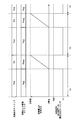
- FIG. 10 is a diagram showing a timing chart of the display system 200 according to the first embodiment.
- the horizontal axis of FIG. 10 is time. 1H shown on the horizontal axis has a time for writing data for one screen into each of the pixels 120, displaying an image, and a time for power generation and power storage. For example, 1H is 1/60 second.
- the period (Ppg) in which power generation and power storage are performed is a period (Pnd) in which image data is not written in the display device 100 and the display device 100 is not displaying.
- the period (Ppng) during which power generation and storage is not performed is the period (Pd) during which an image is written and displayed.
- the control signal for sending image data to the display device 100 is at the low level (Lo) during the period (Ppg) for generating and storing electricity.
- the control signal is generated by the signal supply circuit 16, for example.
- the generated control signal is output from the signal supply circuit 16 and input to the image signal line drive circuit 124, the scanning signal line drive circuit 126, and the scanning signal line drive circuit 128 via the terminal electrode 140.
- the low level (Lo) is 0V, for example.
- the low level (Lo) is 0 [V] in the example, it is not limited to 0 [V].
- the low level (Lo) may be a constant voltage other than 0 [V]. Further, for example, the low level (Lo) may change based on the voltage level of the image data.
- the control signal is at a high level (High) during the period (Ppng) when power generation and storage are not performed.
- the high level (High) is larger than the low level (Lo).
- the high level (High) is, for example, 3 [V] or 3.3 [V].
- the display device 100 is a passive type display device
- one of the first electrode 32 and the second electrode 72 shown in FIG. 5 is connected to the first wiring electrode 22a and the first wiring electrode 22b of the power generating element 250. You may share with either one of. At this time, it is preferable to share an electrode to which a GND potential or a potential close to the GND potential is supplied.
- the timing chart illustrated in FIG. 10 by driving the display system 200, it is possible to independently control the period (Ppg) in which power generation and power storage are performed and the period (Pd) in which an image is written and displayed.
- the influence of the power generation of the power generation element 250 on the power source and the influence of the image display of the display device 100 on the power source can be considered independently. That is, in each period, power can be stably supplied to the power generating element 250 or the display device 100.
- the second electrode 72 may be shared with either the first wiring electrode 22a or the first wiring electrode 22b of the power generating element 250.
- the second electrode 72 is preferably supplied with, for example, a common potential, a GND potential, or a potential close to the GND potential.
- Ppg the period in which power generation and power storage are performed
- Pd the period in which an image is written and displayed.
- the influence of the power generation of the power generation element 250 on the power source and the influence of the image display of the display device 100 on the power source can be considered independently. That is, in each period, power can be stably supplied to the power generating element 250 or the display device 100.
- the display system 200 according to the embodiment of the present invention can generate electric power by being driven using a timing chart as shown in FIG.
- the generated power can be stored, and the display device 100 can be driven by the stored power.
- the drive of the display system 200 according to the embodiment of the present invention by separately providing the period of power generation and storage and the period of displaying an image, it is possible to clearly separate generation of power and image display. It is possible to prevent the power supply from becoming unstable.
- the timing chart shown in FIG. 10 is an example of a timing chart for driving the display system 200 according to the embodiment of the present invention.
- the display system 200 according to the embodiment of the present invention may be driven so as to directly supply the generated power to the display device 100 without storing the generated power.
- an external power supply is not required, so that the manufacturing cost of the display system 200 can be suppressed. Further, the display system 200 can be reduced in weight.
- the present invention it is possible to provide a display device and a display system in which the power generation unit and the display device are integrally formed, instead of separately providing and assembling the power generation unit and the display device. That is, according to the present invention, it is possible to provide a display device and a display system having a built-in power generation unit.
- Second Embodiment a configuration of a display device 300 according to an embodiment of the present invention will be described.
- the configuration of the display device 300 is the same as or similar to the configuration of the display device 100 shown in the first embodiment except that it has a first insulating layer 310 and a second insulating layer 320. Since this is a configuration, description thereof is omitted here.
- FIG. 11 is a perspective view showing the configuration of the display device 300 according to the second embodiment.
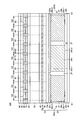
- FIG. 12 is a cross-sectional view showing the configuration of the display device 300 according to the second embodiment.
- the first insulating layer 310 has a role of absorbing heat and transmitting the absorbed heat to the power generation element 250 included in the power generation layer 20.
- the material forming the first insulating layer 310 may be a material that can absorb heat and transfer the absorbed heat to the power generation element 250.
- the material forming the first insulating layer 310 is, for example, a fibrous organic insulating material such as cashmere or silk.
- the first insulating layer 310 is composed of one layer, but the first insulating layer 310 is not limited to this example.
- the first insulating layer 310 may be composed of two or more layers. Specifically, the first insulating layer 310 may be formed by stacking two different organic insulating materials among the organic insulating materials.
- the first insulating layer 310 is composed of a plurality of layers, the layers become thicker, and thus more heat can be transferred to the power generation element 250. Therefore, the amount of heat generated by the display device 300 also increases, and the power generation element 250 can generate larger power.
- the second insulating layer 320 has a role of absorbing moisture or an aqueous solution, for example.
- the material forming the second insulating layer 320 may be a material capable of absorbing water or an aqueous solution. In this specification and the like, the second insulating layer 320 may be referred to as a water absorbent member.
- the material forming the second insulating layer 320 is, for example, an organic insulating material such as polyimide, polyvinyl alcohol, or a polyacrylate-based material.
- the second insulating layer 320 is composed of one, but like the first insulating layer 310, the second insulating layer 320 is also composed of two or more layers. May be.
- the second insulating layer 320 is composed of a plurality of layers, the thickness of the second insulating layer 320 is increased, so that the moisture absorption rate of the second insulating layer 320 is improved. Therefore, in the display device 300, the first insulating layer 310 can transfer a larger amount of heat absorbed by the second insulating layer 320 to the power generation element 250. As a result, the power generation element 250 can generate larger electric power.
- the water absorption of the second insulating layer 320 is higher than that of the first base material 10.
- the material forming the second insulating layer 320 may be a material having adhesiveness.
- the material having adhesiveness is, for example, urethane resin.
- the display device 300 may have an insulating layer in which a material forming the first insulating layer 310 and a material forming the second insulating layer 320 are mixed.
- the mixed material the material for forming the first insulating layer 310 and the second insulating layer 320 can be provided as one insulating layer in the display device 300; therefore, the manufacturing of the display device 300 can be simplified.
- the display device 300 can be used, for example, as a number worn by a track and field athlete.
- the heat of water or aqueous solution generated by the athlete is transferred to the power generating element 250 through the first insulating layer 310 and the second insulating layer, and the power generated by the power generating element 250 is used for the bib number or the company name of the athlete or The school name and the like can be displayed on the display device 300.
- the display device 300 can be used for traceability such as an ecological survey and health management of an animal by being attached to a part of the body of the animal, for example.
Landscapes
- Physics & Mathematics (AREA)
- General Physics & Mathematics (AREA)
- Engineering & Computer Science (AREA)
- Theoretical Computer Science (AREA)
- Power Engineering (AREA)
- Devices For Indicating Variable Information By Combining Individual Elements (AREA)
- Electroluminescent Light Sources (AREA)
- Electric Clocks (AREA)
Abstract
反射型表示装置は、発電素子を含む発電部と、複数の画素および絶縁層を含む表示部と、を有し、絶縁層は第1面および第1面とは反対側の第2面を有し、複数の画素は第1面に設けられ、発電部は第2面に接する。表示装置は、さらに、基材を有し、発電部は基材と表示部との間に設けられてもよい。発電素子は熱を与えられることで起電力を生じてもよい。表示装置は、さらに、複数の駆動回路を有し、複数の駆動回路の一部の電源と発電部の電源とは共有されてもよい。
Description
本発明は、表示装置および表示システムに関する。
携帯電話機や携帯情報端末といった携帯電子機器等の表示装置には、液晶表示装置、有機エレクトロルミネッセンス表示装置等が用いられている。携帯電子機器等の表示装置において、表示装置を駆動するための電力または電圧は、表示装置とは別に設けられた電源装置(例えば、バッテリーなど)から供給される。近年、表示装置の多様化、高速大容量のネットワークの普及により、腕、体、頭などの身体に装着して利用される表示装置、所謂、ウェアラブル装置の利用が進められている。
特許文献1には、太陽電池または温度差またはローターの回転運動により発電を行う機能と時刻表示部を有する腕時計装置が開示されている。前記腕時計装置は、発電によって生成された電力または電圧を用いて駆動する。また、前記腕時計装置は、発電状況、電気容量、または時刻表示部の停止等の異常を表示する機能を有する。
特許文献1に記載の腕時計装置において、発電を行う機能を有する部分と表示部とは別々に形成される。
本発明の課題の一つは、発電部を内蔵した表示装置、および表示システムを提供することにある。
反射型表示装置であって、発電素子を含む発電層部と、複数の画素および絶縁層を含む表示部と、を有し、絶縁層は第1面および第1面とは反対側の第2面を有し、複数の画素は第1面に設けられ、発電部は前記第2面に接する。
表示システムであって、発電素子を含む発電部と、複数の画素および絶縁層を含む表示部と、発電部および表示部と電気的に接続され、発電部から表示部に発電素子によって生成された起電力を供給することを制御する制御装置と、を有し、絶縁層は第1面および第1面とは反対側の第2面を有し、複数の画素は第1面に設けられ、発電部は第2面に接する。
以下、本発明の実施形態を、図面等を参照しながら説明する。但し、本発明は多くの異なる態様で実施することが可能であり、以下に例示する実施の形態の記載内容に限定して解釈されるものではない。また、図面は説明をより明確にするため、実際の態様に比べ、各部の構成等について模式的に表される場合があるが、あくまで一例であって、本発明の解釈を限定するものではない。さらに、本明細書と各図において、既出の図に関して前述したものと同様の要素には、同一の符号(または数字の後にa、bなどを付した符号)を付して、詳細な説明を適宜省略することがある。なお、各要素に対する「第1」、「第2」と付記された文字は、各要素を区別するために用いられる便宜的な標識であり、特段の説明がない限りそれ以上の意味を有さない。
本明細書において、ある部材又は領域が他の部材又は領域の「上に(又は下に)」あるとする場合、特段の限定がない限りこれは他の部材又は領域の直上(又は直下)にある場合のみでなく他の部材又は領域の上方(又は下方)にある場合を含み、すなわち、他の部材又は領域の上方(又は下方)において間に別の構成要素が含まれている場合も含む。なお、以下の説明では、特に断りのない限り、断面視においては、第1基材に対して第2基材が配置される側を「上」又は「上方」といい、その逆を「下」又は「下方」として説明する。
本明細書において説明される第1基材は、少なくとも平面状の一主面を有し、この一主面上に絶縁層、半導体層および導電層の各層、あるいはトランジスタおよび発光素子等の各素子が設けられるものとする。
1.第1実施形態
本実施形態では、本発明の一実施形態に係る表示装置および表示装置システムの構成を説明する。本発明の一実施形態に係る表示装置は、一例として、液晶表示装置である。
本実施形態では、本発明の一実施形態に係る表示装置および表示装置システムの構成を説明する。本発明の一実施形態に係る表示装置は、一例として、液晶表示装置である。
図1は、本発明の一実施形態に係る表示装置の構成を示す模式的な斜視図である。図2は、本発明の一実施形態に係る表示装置100の構成を示す模式的な断面図である。図3は、本発明の一実施形態に係る表示システム200の模式的な平面図である。図2は図1の一部の領域に沿った断面を示す断面図であり、図2は図3に示すB領域のA1-A2に沿った断面を示す断面図でもある。
1-1.表示装置100の構成
図1および図2を用いて、本発明の一実施形態に係る表示装置100の構成を説明する。
図1および図2を用いて、本発明の一実施形態に係る表示装置100の構成を説明する。
図1に示されるように、表示装置100は、第1基材10、発電層20、アレイ層30、第2基材90、および偏光板95を有する。
発電層20が第1基材10の上に設けられる。アレイ層30が発電層20の上に接するように設けられる。偏光板95が第2基材90の上に設けられる。
詳細は後述するが、発電層20は、発電素子250を含む。発電素子250は、例えば、熱電素子(熱電変換素子とも呼ばれる)である。一例として、熱電素子は、n型半導体部と、p型半導体部とを含む。n型半導体部と、p型半導体部とは、電気的に接続される。n型半導体部はn型半導体材料によって形成され、p型半導体部はp型半導体材料によって形成される。n型半導体部とp型半導体部とに一対の電極を設け、熱を発電素子250に与えることで、前記一対の電極間に電位差が生じる。よって、発電素子250は、電力を生成することができる。この効果は、ゼーベック効果と呼ばれる。ゼーベック効果は、公知の効果であるから、ここでの詳細な説明は省略する。表示装置100は、発電素子250を内蔵することによって、電力を生成することができる。詳細は後述するが、生成された電力は、後述する表示システム200によって蓄電され、表示システム200は前記電力を表示装置100の駆動のために利用することができる。なお、図1に例示した表示装置100は、発電素子250を4個有するが、発電素子250の個数、サイズを含む構成はこの例に限定されない。また、発電素子250の構成の一例として、n型半導体部と、p型半導体部とを含む例を示したが、発電素子250の構成はここで示した例に限定されない。発電素子250の構成は、異なる種類の金属を材料として含む二つの部材を接続する構成であってもよい。発電素子250の構成は、熱を与えられることで電力または電圧などを生成することが可能な構成であればよい。また、発電素子250の構成は、本発明の構成を逸脱しない範囲において、表示装置100の用途または仕様などによって、適宜決められればよい。なお、本明細書等において、生成される電力は起電力と言い換えてもよい。
アレイ層30は、下地層138、画像信号線駆動回路124、走査信号線駆動回路126、走査信号線駆動回路128、端子電極140、および周辺領域136を有する。画像信号線駆動回路124、走査信号線駆動回路126、走査信号線駆動回路128、端子電極140、および周辺領域136は、下地層138の上に設けられる。
図1において、図面を見やすくするため、表示部122は、平面的に図示されている。表示部122は、表示装置100に画像を表示するための複数の画素120を有し、実際は、アレイ層30、第1配向膜40、液晶層50、第2配向膜60、第2電極層70、カラーフィルタ層80、および第2基材90の一部を含む。表示部122は発電層20に接するように設けられる。
下地層138は、第1面138aおよび第2面138bを有する。第2面138bは第1面138aに対して略180度反対の面、すなわち、第2面138bは第1面138aとは反対側の面である。第1面138aは絶縁層36に接する。第2面138bは発電層20に接する。
下地層138は、絶縁層である。下地層138を形成する材料は、例えば、酸化ケイ素や窒化酸化ケイ素、酸化窒化ケイ素、窒化ケイ素、酸化アルミニウム等の無機化合物を含む材料である。本発明の一実施形態においては、下地層138は、一つの層で形成される例を示すが、この例に限定されない。例えば、下地層138は、複数の無機化合物を含む材料で形成された層が積層された構造を有していてもよい。具体的には、下地層138は、酸化ケイ素で形成された層と窒化ケイ素で形成された層とを積層し、形成されてもよい。また、下地層138を形成する材料は、有機絶縁材料でもよい。また、下地層138は、無機化合物を含む材料で形成された層と有機絶縁材料で形成された層とが積層された構造を有していてもよい。発電層20およびアレイ層30に含まれる層との密着性、不純物の拡散、不純物の侵入を考慮して適宜選択されればよい。
また、図2に示されるように、第1配向膜40、液晶層50、第2配向膜60、第2電極層70、およびカラーフィルタ層80が、アレイ層30と第2基材90との間に設けられる。アレイ層30は、複数の第1電極が形成される第1電極層34と、絶縁膜が形成される絶縁層36とを含む。第1配向膜40がアレイ層30の上に設けられる。第1配向膜40は、第1電極層34と液晶層50と対向する側に設けられる第2電極層70とを絶縁する役割を有する。
図2を用いて、第1基材10の上面に対向するように設けられる対向側の基板を説明する。対向側基板は、例えば、第2配向膜60、第2電極層70、カラーフィルタ層80、第2基材90、および偏光板95を有する。
偏光板95が第2基材90の上に設けられる。カラーフィルタ層80が第2基材90の下に設けられる。カラーフィルタ層80は、赤色カラーフィルタ層82、緑色カラーフィルタ層84、および青色カラーフィルタ層86を含む。遮光層88が各カラーフィルタ層の間に設けられてもよい。
第2電極層70が、カラーフィルタ層80の下に設けられる。第2電極層70は、複数の第2電極72を含む。画素120は、一つの第1電極32と、前記一つの第1電極32と対向する一つの第2電極72とを含む。
表示装置100は、対向側基板と、第1基材10に第1配向膜40までを設けた基板と、張り合わせることによって、製造される。対向側基板と、第1基材10に第1配向膜40までを設けた基板とは、シール材などを用いて、張り合わせることができる。液晶層50は、対向側基板と、第1基材10に第1配向膜40までを設けた基板との間に設けられる。第1基材10および第2基材は可撓性を有してもよい。第1基材10および第2基材が可撓性を有することによって、表示装置100は可撓性を有する。よって、表示装置100は人体などの曲面に取り付けられるウェアラブル装置として利用できる。なお、第1基材10および第2基材が可撓性を有する場合、第1基材10および第2基材に用いられる材料は例えばポリイミドである。
表示装置100はパッシブ型表示装置でもよく、アクティブ型表示装置でもよい。例えば、表示装置100がパッシブ型表示装置の場合、アレイ層30は、少なくとも、複数の第1電極32が形成される第1電極層34と、絶縁膜が形成される絶縁層36とを含む。第2電極層70は、複数の第2電極72を含む。画素120は、一つの第1電極32と、前記一つの第1電極32と対向する一つの第2電極72とを含む。一つの第1電極32と、前記一つの第1電極32と対向する一つの第2電極72とのそれぞれに、電圧が印加されることによって、表示装置100は画像を表示することができる。なお、第2電極層70は、隣接する第2電極を絶縁するための絶縁層を含んでもよい。
また、図示は省略するが、表示装置100がアクティブ型表示装置の場合、アレイ層30は、複数の薄膜トランジスタ(Thin Film Transistor、TFT)、および複数の容量素子を含む。画素120は、一つのTFTに電気的に接続された一つの第1電極32と、前記一つの第1電極32と対向する一つの第2電極72とを含む。一つの第1電極32と、前記一つの第1電極32と対向する一つの第2電極72とのそれぞれに、電圧が印加されることによって、表示装置100は画像を表示することができる。なお、TFTは、例えば、半導体層、ゲート絶縁膜、ゲート電極、層間膜、およびソースドレイン電極を含む。TFTの製造において、TFTの形成方法、薄膜トランジスタまたは容量素子の構造、それぞれの膜、層、および各部分の材料は、本発明の技術分野で通常使用される公知技術を採用することができる。よって、本明細書中において、TFTの製造方法の説明は省略される。
なお、表示装置100は透過型表示装置でもよいし、反射型表示装置でもよいし、半透過型表示装置でもよい。表示装置100が反射型表示装置の場合、バックライトを必要としないため、表示装置100の軽量化、低消費電力化、製造コスト低減が可能となる。また、画素の構造はIPSモードに対応した構造でもよいし、VAモードに対応した構造でもよい。画素の構造は、表示システム200で画像を表示することが可能な構造であればよい。
例えば、表示装置100が透過型表示装置の場合、表示装置100の発電素子250が設けられている側にバックライトを配置し、バックライトの熱で発電素子250が生成した電力によって、映像を表示装置300に表示することができる。また、表示装置100は窓ガラスまたは車のフロントガラスに張り付けることによって、日光が窓ガラスまたは車のフロントガラスにあたり、日光の熱で発電素子250が生成した電力によって、映像を表示装置100に表示することができる。
また、本発明の一実施形態に係る表示装置の製造方法は、特に説明の無い限り、表示装置の製造において一般的に用いられるフォトリソグラフィー技術を利用することができる。また、本発明の技術分野で使用される製造方法は、本発明の一実施形態に係る表示装置の製造方法に採用することができる。TFTの製造と同様に、それぞれの膜、層、および各部分の材料は、本発明の技術分野で通常使用される公知技術を採用することができる。よって、本明細書中において、表示装置の製造方法の説明は省略される。
以降の説明においては、表示装置100がパッシブ型表示装置である例を説明する。
1-2.表示システム200の構成
図3を用いて、本発明の一実施形態に係る表示システム200の構成を説明する。図1または図2と同一、または類似する構成については説明を省略することがある。
図3を用いて、本発明の一実施形態に係る表示システム200の構成を説明する。図1または図2と同一、または類似する構成については説明を省略することがある。
複数の画素120が、表示部122に設けられる。走査信号線駆動回路126(走査信号線駆動回路128は省略)および画像信号線駆動回路124は、周辺領域136に設けられる。走査信号線駆動回路126および画像信号線駆動回路124は、画素120の駆動を制御する。図2においては、走査信号線駆動回路126および画像信号線駆動回路124は、ICチップを用いた例を示す。また、図2においては、走査信号線駆動回路126および画像信号線駆動回路124は、第1基材10の上に設けられる例を示すが、この例に限定されない。例えば、第1基材10とは異なる基板(半導体基板など)の上に形成された駆動回路を、第1基材10またはフレキシブルプリント回路(Flexible Printed Circuit、FPC)基板などのコネクタ214の上に設けてもよい。また、走査信号線駆動回路126および画像信号線駆動回路124が有する回路の一部または全部を第1基材10とは異なる基板の上に形成し、第1基材10またはコネクタ214の上に設ける構成としてもよい。また、走査信号線駆動回路126に含まれる駆動回路あるいは駆動回路の一部が、第1基材10の上に直接形成されてもよい。なお、ここでは図示していないが、第1基材10の上には、画素120内に設けられる液晶素子などの表示素子、およびそれらを制御するための各種半導体素子が形成される。
また、表示システム200は、第1の配線206、コンタクトホール208、第1の端子配線210、第1の端子212、第2の配線216、コンタクトホール218、第2の端子配線220、第2の端子222なども有する。これらも、第1基材10の上に設けられる。
発電素子250は、周辺領域136から延びる第1の配線206と電気的に接続される。第1の配線206は周辺領域136を延伸し、コンタクトホール208を介して第1の端子配線210と電気的に接続される。第1の端子配線210は表示装置100の端部付近で露出され、第1の端子212を形成する。第1の端子212はコネクタ214と接続される。
発電素子250が第1の配線206に電気的に接続されることで、発電素子250が生成した電力をコネクタ214を介して、制御装置400に供給することができる。制御装置400に供給された電力は、制御装置400が有する蓄電部14に蓄電される。前記電力によって、表示装置100を駆動することができる。
画素120を駆動するための信号または電源が、制御装置400から、周辺領域136から延びる第2の配線216を介して画素120に供給されてもよい。画素120は、周辺領域136から延びる第2の配線216と電気的に接続される。第2の配線216は周辺領域136を延伸し、コンタクトホール218を介して第2の端子配線220と電気的に接続される。第2の端子配線220は表示装置100の端部付近で露出されて第2の端子222を形成する。第2の端子222はコネクタ214と接続される。
画素120を駆動するための信号または電源が、制御装置400から第1の端子212または第2の端子222、走査信号線駆動回路126および画像信号線駆動回路124を経由して、画素120に供給される。第1の端子212または第2の端子222は、表示装置100の一つの辺に並ぶように形成することができる。このため、単一のコネクタ214を用いて、表示部122、走査信号線駆動回路126および画像信号線駆動回路124の各々に、独立して、電圧や信号を供給することができる。
図2に図示されるように、表示部122には、複数の画素120が、互いに交差するに方向(例えば、互いに交差するX方向及びY方向)に沿うようにマトリクス状に配置される。図2においては、画素120の配列は、ストライプ配列である例を示している。画素120のそれぞれは、例えば、三つの副画素130、副画素132、副画素134に対応していてもよい。三つの副画素で一つの画素が形成されてもよい。各副画素には液晶素子などの表示素子が一つ備えられる。副画素が対応する色は液晶素子、または副画素上に設けられるカラーフィルタの特性によって決定される。本明細書等では、画素120のそれぞれが液晶素子を有する例を示す。画素120は、表示部122で再現される画像の一部を構成する最小単位である。表示部122が有する副画素はいずれかの画素に含まれる。
また、ストライプ配列では、三つの副画素130、副画素132、副画素134が互いに異なる色を与えるように構成することができる。例えば、副画素130、副画素132、副画素134にそれぞれ、赤色、緑色、青色の三原色を発するカラーフィルタ層を備えることができる。そして、三つの副画素のそれぞれに任意の電圧あるいは電流を供給することで、フルカラーの表示装置を提供することができる。
制御装置400は、少なくとも、蓄電部14と、信号供給回路16と、電源回路22とを有する。また、制御装置400はコネクタ224を介して外部電源装置410と電気的に接続されている。
信号供給回路16は、映像信号、および表示装置100を駆動するための信号を生成することができる。信号供給回路16は、信号を一つ以上生成することができる。また、前記生成された信号は、複数の同じ信号であってもよく、お互いに異なる複数の信号であってもよく、同じ信号と、お互いに異なる複数の信号であってもよい。信号供給回路16が生成する信号は、本発明に係る構成を逸脱しない範囲において、適宜選択されればよい。前記生成された信号が表示部122、走査信号線駆動回路126および画像信号線駆動回路124の各々に供給される。
蓄電部14は、発電素子250によって生成された電力を蓄電することができる。蓄電部は、例えば、電界コンデンサまたはセラミックコンデンサを有する。また、前記電力によって、表示装置100を駆動することができる。なお、発電素子250が表示装置100を駆動するための十分な電力を生成することができるとき、表示システム200は、蓄電部14を備えなくてもよい。表示システム200は、蓄電部14を備えないことによって、発電素子250が生成した電力を蓄電することなく、後述する電源回路22に直接供給することができる。したがって、表示システム200は、蓄電部14を備えないことによって、表示システム200の製造コストを抑えることができる。
電源回路22は、信号供給回路16、および表示装置100に電力を供給する。電源回路22は、蓄電部14に蓄電された電力に基づき、表示装置100、走査信号線駆動回路126および画像信号線駆動回路124に供給する電源に相当する電圧を生成することができる。電源回路22は、例えば、DC-DC変換回路、チャージポンプ回路などを含む。
外部電源装置410は、電源回路22と同様に、走査信号線駆動回路126および画像信号線駆動回路124に供給する電源に相当する電圧を生成し、信号供給回路16、および表示装置100に電力を供給することができる。なお、発電素子250が表示装置100を駆動するための十分な電力を生成することができるとき、外部電源装置410は、表示装置100に電力を供給しなくてもよい。また、発電素子250が表示装置100を駆動するための十分な電力を生成することができるとき、表示システム200は、外部電源装置410を備えなくてもよい。したがって、表示システム200は、外部電源装置410を備えないことによって、表示システム200の製造コストを抑えることができる。
コネクタ224も、コネクタ214と同様にFPCを用いることができる。コネクタ214は、映像信号、回路の動作を制御するタイミング信号、電源などを、表示装置100、走査信号線駆動回路126および画像信号線駆動回路124に供給する役割も有する。
1-3.発電層20の構成
図4は、第1実施形態に係る発電層20の構成を示す平面図である。発電層20と、発電層20とコネクタ214の接続に関連する構成以外は、図1乃至図3と同一、または類似する構成であるから、ここでの説明を省略する。なお、図4を見やすくするため、図4は、図3に図示されていたコネクタ224、外部電源装置410、画素120、下地層138などを省略している。なお、本明細書等において、発電層は発電部と言い換えてもよい。
図4は、第1実施形態に係る発電層20の構成を示す平面図である。発電層20と、発電層20とコネクタ214の接続に関連する構成以外は、図1乃至図3と同一、または類似する構成であるから、ここでの説明を省略する。なお、図4を見やすくするため、図4は、図3に図示されていたコネクタ224、外部電源装置410、画素120、下地層138などを省略している。なお、本明細書等において、発電層は発電部と言い換えてもよい。
発電層20は発電素子250aを含む。発電素子250aは、第1配線電極22a、第1配線電極22b、p型半導体部24、第2配線電極26、およびn型半導体部28を含む。
第1配線電極22aは、第1の配線206と電気的に接続される。p型半導体部24の第1端子は、第1配線電極22aに電気的に接続される。p型半導体部24の第2端子は、第2配線電極26に電気的に接続される。n型半導体部28の第1端子は、第2配線電極26に電気的に接続される。n型半導体部28の第2端子は、第1配線電極22bに電気的に接続される。第1配線電極22bは、第1の配線206と電気的に接続される。
第1配線電極22aおよび第1配線電極22bを形成する材料は、例えば、銅、アルミニウム、銀、などのように、熱伝導率の高い材料を用いればよい。第2配線電極26を形成する材料も第1配線電極22aおよび第1配線電極22bと同様の材料を用いればよい。
p型半導体部24を形成する材料は、例えば、p型キャリアを添加したPbTeSe、SiGe、などのように、電気伝導率の高い材料を用いればよい。また、n型半導体部28を形成する材料は、例えば、n型キャリアを添加したPbTeSe、SiGe、などのように、電気伝導率の高い材料を用いればよい。本明細書等において、発電素子を形成する半導体部を発電部材と呼ぶことがある。
なお、発電素子250の構成の一例として、n型半導体部と、p型半導体部とを含む例を示したが、発電素子250の構成はここで示した例に限定されない。発電素子250の構成は、異なる種類の金属を材料として含む二つの部材を接続する構成であってもよい。異なる種類の金属を材料は、例えば、カリウム、アルミニウム、銅などのように、電気伝導率の高い材料を用いればよい。
発電素子250aに熱が与えられることで第1配線電極22aと第1配線電極22bとの間に電位差が生じる。例えば、第2配線電極26に熱が与えられることで、第2配線電極26と第1配線電極22aおよび第1配線電極22bとの間に温度差が生じるため、第1配線電極22aと第1配線電極22bとの間に電位差が生じる。よって、発電素子250aは、電力を生成することができる。
ここで、前記温度差をΔT[K]、前記電位差をΔV[V]、ゼーベック係数をSとすると、数式(1)のような関係がある。

また、発電素子250a(熱電素子)の性能は、以下の数式(2)の熱電性能指数Z[1/K]で表すことができる。

ここで、Sはゼーベック係数、σは電気伝導率、κは熱伝導率である。
図4においては、発電素子250aは第1基材10の上面の一部に設けられる例が示されるが、この例に限定されない。発電素子250aは、第1基材10の全面に設けられてもよい。発電素子250aの面積が大きくなることで、発電素子250aの電気伝導率が向上するため、数式(2)に示す熱電性能指数Zを大きくすることができる。すなわち、発電素子250aの面積が大きくなることで、発電効率を向上させることができる。
また、第1配線電極22aは、第1の配線206、コンタクトホール208、第1の端子配線210、第1の端子212、およびコネクタ214を介して、表示システム200におけるGND端子に電気的に接続してもよい。画像信号線駆動回路124もGND端子に電気的に接続される。よって、画像信号線駆動回路124と第1配線電極22aとは、GND端子を共用することができる。図示はしていないが、画像信号線駆動回路124と第1配線電極22aと走査信号線駆動回路126とで、GND端子を共用することもできる。表示システム200において、各回路または各部分においてGND端子を共用することで、端子の数を減らすことができるため、表示装置100の製造コストを低減できる。また、各回路または各部分においてGND端子を共用することで、各回路または各部分は同一のGND端子からGND電位を供給される。その結果、各回路または各部分において、GND電位のばらつきを少なくすることができる。各回路または各部分において、GND電位を揃えることで、基準電位を揃えることができる。
図5は、第1実施形態に係る発電層20の構成を示す断面図であり、図4のB1-B2に沿った断面図である。図4のB1-B2に沿った断面は、表示装置100のY方向に沿って平行または略平行な面である。
発電素子250aは、第1配線電極22a、第1配線電極22b、p型半導体部24、第2配線電極26、およびn型半導体部28を含む。p型半導体部24の第1端子24-1は、第1配線電極22aに電気的に接続される。p型半導体部24の第2端子24-2は、第2配線電極26に電気的に接続される。n型半導体部28の第1端子28-1は、第2配線電極26に電気的に接続される。n型半導体部28の第2端子28-2は、第1配線電極22bに電気的に接続される。絶縁膜27がp型半導体部24とn型半導体部28との間に設けられる。換言すると、p型半導体部24およびn型半導体部28は絶縁膜27に囲まれている。また、絶縁膜27は第1配線電極22aと第1配線電極22bとの間にも設けられる。すなわち、p型半導体部24とn型半導体部28とは、第1基材10の上に離隔するように設けられ、第2配線電極26によって電気的に接続され、絶縁膜27によって絶縁されている。また、図示はしていないが、絶縁膜27の一部は周辺領域136において、第1基材10と接するように設けられている。なお、本明細書等において、絶縁膜27を絶縁部材と呼ぶことがある。
表示装置100のY方向に設けられた8個の画素120のそれぞれは、第1電極32と、前記第1電極32と対向する第2電極72とを含む。
図6は、第1実施形態に係る発電層20の構成を示す断面図であり、図4のC1-C2に沿った断面図である。図4のC1-C2に沿った断面は、表示装置100のX方向に沿って平行または略平行な面である。
発電素子250aは、第1配線電極22b、第2配線電極26、およびn型半導体部28を含む。n型半導体部28の第1端子28-1は、第2配線電極26に電気的に接続される。n型半導体部28の第2端子28-2は、第1配線電極22bに電気的に接続される。絶縁膜27がn型半導体部28を囲うように設けられている。なお、図示はされていないが、n型半導体部28と同様に、絶縁膜27がp型半導体部24も囲うように設けられている。
表示装置100のX方向に設けられた9個の画素120のそれぞれは、第1電極32と、前記第1電極32と対向する第2電極72とを含む。第1電極32は9個の画素120に共有される。
また、図4に示すように、発電素子250aは、表示部122の下方に、表示部122と重なるように設けられる。また、図5および図6に示すように、発電素子250aは、複数の画素120の下方に、複数の画素120と重なるように設けられる。発電素子250aは、複数の画素120と重なることで、複数の画素120を駆動したときの熱によって、より大きな電力を生成することができる。
なお、発電層20は、表示装置の製造において一般的に用いられるフォトリソグラフィー技術を利用することができる。また、発電層20は、例えば、液晶滴下装置、インクジェット印刷機、またはスクリーン印刷機を用いて形成されてもよい。さらに、発電層20は、電界メッキを用いて形成されてもよい。発電層20は、本発明の技術分野で使用される製造方法によって形成される。したがって、発電層20および表示部を含むアレイ層は、TFTの製造と同様に、それぞれの膜、層、および各部分の材料は、本発明の技術分野で通常使用される公知技術を採用することができる。よって、本明細書中において、発電層20の製造方法の詳細な説明は省略される。
1-4.発電層20の構成の変形例
図7は、第1実施形態に係る発電層20の構成を示す平面図である。発電層20が、発電素子250aと、発電素子250bと、発電素子250cと、を含む。発電層20は3個の発電素子250を有する構成以外は、図4の構成と同一、または類似する構成であるから、ここでの説明を省略する。また、図1乃至図3、図5および図6と同一、または類似する構成については省略することがある。
図7は、第1実施形態に係る発電層20の構成を示す平面図である。発電層20が、発電素子250aと、発電素子250bと、発電素子250cと、を含む。発電層20は3個の発電素子250を有する構成以外は、図4の構成と同一、または類似する構成であるから、ここでの説明を省略する。また、図1乃至図3、図5および図6と同一、または類似する構成については省略することがある。
発電層20は発電素子250aと、発電素子250bと、発電素子250cと、を含む。発電素子250aは、第1配線電極22a、第1配線電極22ab、p型半導体部24a、第2配線電極26a、およびn型半導体部28aを含む。発電素子250bは、第1配線電極22ab、第1配線電極22bc、p型半導体部24b、第2配線電極26b、およびn型半導体部28bを含む。発電素子250cは、第1配線電極22bc、第1配線電極22c、p型半導体部24c、第2配線電極26c、およびn型半導体部28cを含む。なお、発電素子250aと、発電素子250bと、発電素子250cとを形成する材料は、図4において説明した材料を用いることができる。
第1配線電極22aは、第1の配線206と電気的に接続される。p型半導体部24aの第1端子は、第1配線電極22aに電気的に接続される。p型半導体部24aの第2端子は、第2配線電極26aに電気的に接続される。n型半導体部28aの第1端子は、第2配線電極26aに電気的に接続される。n型半導体部28aの第2端子は、第1配線電極22abに電気的に接続される。p型半導体部24bの第1端子は、第1配線電極22abに電気的に接続される。p型半導体部24bの第2端子は、第2配線電極26bに電気的に接続される。n型半導体部28bの第1端子は、第2配線電極26bに電気的に接続される。n型半導体部28bの第2端子は、第1配線電極22bcに電気的に接続される。p型半導体部24cの第1端子は、第1配線電極22bcに電気的に接続される。p型半導体部24cの第2端子は、第2配線電極26cに電気的に接続される。n型半導体部28cの第1端子は、第2配線電極26cに電気的に接続される。n型半導体部28cの第2端子は、第1配線電極22cに電気的に接続される。第1配線電極22cは、第1の配線206と電気的に接続される。
以上のようにして、発電素子250aと、発電素子250bと、発電素子250cとが電気的に接続される。発電素子250aと、発電素子250bと、発電素子250cとに熱が与えられることで、第1配線電極22aと第1配線電極22cとの間に電位差が生じる。よって、発電素子250aと、発電素子250bと、発電素子250cとは、電力を生成することができる。
図7においては、発電素子250aと、発電素子250bと、発電素子250cとは第1基材10の上面の一部に設けられる例が示されるが、この例に限定されない。発電素子250aと、発電素子250bと、発電素子250cとは、第1基材10の全面に設けられてもよい。発電素子250aと、発電素子250bと、発電素子250cとの面積が大きくなることで、発電素子250aと、発電素子250bと、発電素子250cとの電気伝導率が向上するため、数式(2)に示す熱電性能指数Zを向上させることができる。すなわち、発電素子250aと、発電素子250bと、発電素子250cとの面積が大きくすることで、発電効率を向上させることができる。
なお、図4と同様に、図7においても、第1配線電極22aは、画像信号線駆動回路124と、GND端子を共用することができる。図4と同様に、図7においても、各回路または各部分においてGND端子を共用することで、端子の数を減らすことができるため、表示装置100の製造コストを低減できる。
図8は、第1実施形態に係る発電層20の構成を示す断面図であり、図7のD1-D2に沿った断面図である。図8のD1-D2に沿った断面は、表示装置100のY方向に沿って平行または略平行な面である。
n型半導体部28aの第1端子28a-1は、第2配線電極26aに電気的に接続される。n型半導体部28aの第2端子28a-2は、第1配線電極22abに電気的に接続される。p型半導体部24cの第1端子24c-1は、第1配線電極22bcに電気的に接続される。p型半導体部24cの第2端子24c-2は、第2配線電極26cに電気的に接続される。絶縁膜27がp型半導体部24cとn型半導体部28aとの間に設けられる。換言すると、p型半導体部24cおよびn型半導体部28aは絶縁膜に囲まれている。また、絶縁膜27は第1配線電極22abと第1配線電極22bcとの間、および、第2配線電極26aと第2配線電極26cとの間にも設けられる。すなわち、n型半導体部28aとp型半導体部24cとは、第1基材10の上に離隔するように設けられ、絶縁膜27によって絶縁されている。また、絶縁膜27の一部は、第1基材10と接するように設けられている。
図9は、第1実施形態に係る発電層20の構成を示す断面図であり、図7のE1-E2に沿った断面図である。図9のE1-E2に沿った断面は、表示装置100のX方向に沿って平行または略平行な面である。
n型半導体部28cの第1端子28c-1は、第2配線電極26cに電気的に接続される。n型半導体部28cの第2端子28c-2は、第1配線電極22cに電気的に接続される。p型半導体部24cの第1端子24c-1は、第1配線電極22bcに電気的に接続される。p型半導体部24cの第2端子24c-2は、第2配線電極26cに電気的に接続される。n型半導体部28bの第1端子28b-1は、第2配線電極26bに電気的に接続される。n型半導体部28bの第2端子28b-2は、第1配線電極22bcに電気的に接続される。絶縁膜27がp型半導体部24cとn型半導体部28cとの間、および、p型半導体部24cとn型半導体部28bとの間、に設けられる。換言すると、p型半導体部24cとn型半導体部28bとn型半導体部28cとは絶縁膜に囲まれている。また、絶縁膜27は第1配線電極22cと第1配線電極22bcとの間、および、第2配線電極26bと第2配線電極26cとの間にも設けられる。すなわち、n型半導体部28bとn型半導体部28cとp型半導体部24cとは、第1基材10の上に離隔するように設けられ、絶縁膜27によって絶縁されている。また、絶縁膜27の一部は、第1基材10と接するように設けられている。
図7に示すように、発電素子250aと、発電素子250bと、発電素子250cとは、表示部122の下方に、表示部122と重なるように設けられる。また、図8および図9に示すように、発電素子250aと、発電素子250bと、発電素子250cとは、複数の画素120の下方に、複数の画素120と重なるように設けられる。発電素子250aと、発電素子250bと、発電素子250cとは、複数の画素120と重なることで、複数の画素120を駆動したときの熱によって、より大きな電力を生成することができる。
さらに、図8および図9に示すように、発電部材(n型半導体部28とp型半導体部24)との一部は絶縁膜(絶縁部材)によって囲まれ、絶縁膜(絶縁部材)の一部は第1基材10と接するように設けられている。絶縁膜(絶縁部材)が第1基材10と接するように設けられることで、第1基材10が熱源に近づくと、熱源が発する熱は第1基材10と絶縁膜(絶縁部材)とを介して、発電部材に伝わり易くなる。よって、表示装置100に含まれる絶縁膜(絶縁部材)27が第1基材10と接するように設けられることで、発電素子250がより電力を生成し易い構成とすることができる。
1-5.表示システム200の駆動方法の例
図10は、第1実施形態に係る表示システム200のタイミングチャートを示す図である。
図10は、第1実施形態に係る表示システム200のタイミングチャートを示す図である。
図10の横軸は時間である。横軸に示した1Hは一画面分のデータを画素120のそれぞれに書き込み、画像を表示する時間と、発電および蓄電を行う時間とを有する。例えば、1Hは1/60秒である。発電および蓄電を行う期間(Ppg)は、表示装置100は画像データを書き込まれておらず、表示装置100は表示をしていない期間(Pnd)である。発電および蓄電を行わない期間(Ppng)は、画像を書き込んで表示している期間(Pd)である。
発電および蓄電を行う期間(Ppg)は、表示装置100に画像データを送るための制御信号はローレベル(Lo)である。制御信号は、例えば、信号供給回路16で生成される。生成された制御信号は、信号供給回路16から出力され、端子電極140を経由して、画像信号線駆動回路124、走査信号線駆動回路126、および走査信号線駆動回路128に入力される。ローレベル(Lo)は例えば0Vである。なお、ローレベル(Lo)は0[V]である例を示したが、0[V]に限定されない。例えば、ローレベル(Lo)は0[V]以外の定電圧でもよい。また、例えば、ローレベル(Lo)は、画像データの電圧レベルに基づき変化してもよい。
発電および蓄電を行わない期間(Ppng)は、制御信号はハイレベル(High)である。ハイレベル(High)はローレベル(Lo)よりも大きな値である。ハイレベル(High)は例えば3[V]または3.3[V]である。
また、表示装置100がパッシブ型表示装置の場合、例えば図5に図示される第1電極32と第2電極72との何れか一方を発電素子250の第1配線電極22aと第1配線電極22bとの何れか一方と共用してもよい。なお、このとき、GND電位またはGND電位に近い電位が供給される電極を共用することが好ましい。図10に図示されたタイミングチャートで、表示システム200を駆動することによって、発電および蓄電を行う期間(Ppg)と画像を書き込んで表示している期間(Pd)とを独立に制御可能なため、発電素子250の発電による電源への影響および表示装置100の画像表示による電源への影響とを独立に考えることができる。すなわち、各期間において、電源を発電素子250または表示装置100に安定供給することができる。
また、表示装置100がアクティブ型表示装置の場合、第2電極72を発電素子250の第1配線電極22aと第1配線電極22bとの何れか一方と共用してもよい。なお、このとき、第2電極72は、例えばコモン電位、GND電位またはGND電位に近い電位が供給されることが好ましい。図10に図示されたタイミングチャートで、表示システム200を駆動することによって、発電および蓄電を行う期間(Ppg)と画像を書き込んで表示している期間(Pd)とを独立に制御可能なため、発電素子250の発電による電源への影響および表示装置100の画像表示による電源への影響とを独立に考えることができる。すなわち、各期間において、電源を発電素子250または表示装置100に安定供給することができる。
本発明の一実施形態に係る表示システム200は、図10に示すようなタイミングチャートを用いて駆動されることで、電力を生成することができる。また、生成された電力を蓄電し、蓄電された電力で表示装置100を駆動することができる。本発明の一実施形態に係る表示システム200の駆動において、発電および蓄電の期間と画像を表示する期間とを、それぞれ独立に設けることによって、電力の生成と画像表示とを明確に分離できるため、電源が不安定になることを抑制できる。
なお、図10に示されたタイミングチャートは、本発明の一実施形態に係る表示システム200を駆動するためのタイミングチャートの一例である。本発明の一実施形態に係る表示システム200は、生成された電力を蓄電せずに、生成された電力を表示装置100に直接供給するように駆動されてもよい。生成された電力を表示装置100に直接供給することで、外部電源が不要となるため、表示システム200の製造コストを抑えることができる。また、表示システム200を軽量化することもできる。
以上の通り、本発明によって、発電部と表示装置とを別々に設けて組み立てるのではなく、発電部と表示装置とが一体形成される表示装置、および表示システムを提供することができる。すなわち、本発明によって、発電部を内蔵した表示装置、および表示システムを提供することができる。
2.第2実施形態
本実施形態では、本発明の一実施形態に係る表示装置300の構成を説明する。表示装置300の構成は、第1実施形態において示された表示装置100の構成とは、第1絶縁層310および第2絶縁層320を有する点以外は、第1実施形態と同一、または類似する構成であるから、ここでの説明を省略する。
本実施形態では、本発明の一実施形態に係る表示装置300の構成を説明する。表示装置300の構成は、第1実施形態において示された表示装置100の構成とは、第1絶縁層310および第2絶縁層320を有する点以外は、第1実施形態と同一、または類似する構成であるから、ここでの説明を省略する。
図11は第2実施形態に係る表示装置300の構成を示す斜視図である。図12は第2実施形態に係る表示装置300の構成を示す断面図である。
第1絶縁層310は、熱を吸収し、吸収した熱を発電層20に含まれる発電素子250に伝達する役割を有する。
第1絶縁層310を形成する材料は、熱を吸収し、吸収した熱を発電素子250に伝達することが可能な材料で有ればよい。第1絶縁層310を形成する材料は、例えば、カシミヤ、絹、などの繊維状の有機絶縁材料である。また、図11および図12に示される例において、第1絶縁層310は一つの層から構成されるが、第1絶縁層310はこの例に限定されない。第1絶縁層310は二つ以上の層から構成されてもよい。具体的には、第1絶縁層310は、前記有機絶縁材料のうち、異なる二つの有機絶縁材料を積層してもよい。第1絶縁層310は複数の層から構成されることによって、層が厚くなるため、より多くの熱を発電素子250に伝達することができる。よって、表示装置300の発熱量も多くなり、発電素子250はより大きな電力を生成することができる。
第2絶縁層320は、例えば、水分または水溶液を吸収する役割を有する。
第2絶縁層320を形成する材料は、水分または水溶液を吸収することが可能な材料で有ればよい。本明細書等において、第2絶縁層320は吸水性部材と呼ぶこともある。第2絶縁層320を形成する材料は、例えば、ポリイミド、ポリビニルアルコール、ポリアクリル酸塩系などの有機絶縁材料である。また、図11および図12に示される例において、第2絶縁層320は一つのから構成されるが、第1絶縁層310と同様に、第2絶縁層320も二つ以上の層から構成されてもよい。第2絶縁層320は複数の層から構成されることによって、層が厚くなるため、第2絶縁層320の水分の吸収率が向上する。よって、表示装置300において、第1絶縁層310は、第2絶縁層320に吸収されたより多くの熱量を、発電素子250に伝達することができる。その結果、発電素子250はより大きな電力を生成することができる。なお、第2絶縁層320の吸水性は、第1基材10の吸水性よりも高い。また、第2絶縁層320を形成する材料は、粘着性を有する材料であってもよい。粘着性を有する材料は、例えば、ウレタン樹脂などである。
なお、表示装置300は、第1絶縁層310を形成する材料と第2絶縁層320を形成する材料とを混合した絶縁層を有していても良い。混合材料を用いることによって、第1絶縁層310を形成する材料と第2絶縁層320とを一つの絶縁層として、表示装置300に設けることができるため、表示装置300の製造を簡略化できる。
表示装置300は、例えば、陸上競技の競技者が装着するゼッケンとして用いることができる。競技者が発する水分または水溶液の熱を第1絶縁層310および第2絶縁層を介して発電素子250に伝達し、発電素子250が生成した電力で、ゼッケン番号や競技者の所属する会社名または学校名等を表示装置300に表示することができる。また、表示装置300は、例えば、動物の体の一部に張り付けることによって、動物の生態調査や健康管理などのトレーサビリティーに利用することができる。
本発明の実施形態として上述した各実施形態は、相互に矛盾しない限りにおいて、適宜組み合わせて実施することができる。
上述した各実施形態の態様によりもたらされる作用効果とは異なる別の作用効果であっても、本明細書の記載から明らかなもの、または、当業者において容易に予測し得るものについては、当然に本発明によりもたらされるものと解される。
10:第1基材、14:蓄電部、16:信号供給回路、20:発電層、22:電源回路、22a:第1配線電極、22ab:第1配線電極、22b:第1配線電極、22bc:第1配線電極、22c:第1配線電極、24:p型半導体部、24-1:第1端子、24-2:第2端子、24a:p型半導体部、24b:p型半導体部、24c:p型半導体部、24c-1:第1端子、24c-2:第2端子、26:第2配線電極、26a:第2配線電極、26b:第2配線電極、26c:第2配線電極、27:絶縁膜(絶縁部材)、27:絶縁膜、28:n型半導体部、28-1:第1端子、28-2:第2端子、28a:n型半導体部、28a-1:第1端子、28a-2:第2端子、28b:n型半導体部、28b-1:第1端子、28b-2:第2端子、28c:n型半導体部、28c-1:第1端子、28c-2:第2端子、30:アレイ層、32:第1電極、34:第1電極層、36:絶縁層、40:第1配向膜、50:液晶層、60:第2配向膜、70:第2電極層、72:第2電極、80:カラーフィルタ層、82:赤色カラーフィルタ層、84:緑色カラーフィルタ層、86:青色カラーフィルタ層、88:遮光層、90:第2基材、95:偏光板、100:表示装置、120:画素、122:表示部、124:画像信号線駆動回路、126:走査信号線駆動回路、128:走査信号線駆動回路、130:副画素、132:副画素、134:副画素、136:周辺領域、138:下地層、138a:第1面、138b:第2面、140:端子電極、200:表示システム、206:第1の配線、208:コンタクトホール、210:第1の端子配線、212:第1の端子、214:コネクタ、216:第2の配線、218:コンタクトホール、220:第2の端子配線、222:第2の端子、224:コネクタ、250:発電素子、250a:発電素子、250b:発電素子、250c:発電素子、300:表示装置、310:第1絶縁層、320:第2絶縁層、400:制御装置、410:外部電源装置
Claims (15)
- 発電素子を含む発電部と、
複数の画素および絶縁層を含む表示部と、
を有し、
前記絶縁層は第1面および前記第1面とは反対側の第2面を有し、
前記複数の画素は前記第1面に設けられ、前記発電部は前記第2面に接する、
反射型表示装置。 - さらに、基材を有し、
前記発電部は前記基材と前記表示部との間に設けられる、
請求項1に記載の反射型表示装置。 - 前記発電素子は熱を与えられることで起電力を生じる、
請求項1に記載の反射型表示装置。 - さらに、複数の駆動回路を有し、
前記複数の駆動回路の一部の電源と前記発電部の電源とは共有される、
請求項1に記載の反射型表示装置。 - 前記発電素子は一対の電極と絶縁部材と発電部材とを有し、
前記発電部材の一部と前記一対の電極とは前記絶縁部材で囲まれ、
前記絶縁部材の一部は、前記基材の一部と接している、
請求項2に記載の反射型表示装置。 - 前記基材は可撓性を有する、
請求項2に記載の反射型表示装置。 - さらに、吸水性部材を有し、
前記吸水性部材は前記基材に接するように設けられる、
請求項2に記載の反射型表示装置。 - 発電素子を含む発電部と、
複数の画素および絶縁層を含む表示部と、
前記発電部および前記表示部と電気的に接続され、前記発電部から前記表示部に前記発電素子によって生成された起電力を供給することを制御する制御装置と、
を有し、
前記絶縁層は第1面および前記第1面とは反対側の第2面を有し、
前記複数の画素は前記第1面に設けられ、前記発電部は前記第2面に接する、
表示システム。 - さらに、基材を有し、
前記発電部は前記基材と前記表示部との間に設けられる、
請求項8に記載の表示システム。 - 前記発電素子は熱を与えられることで起電力を生じる、
請求項8に記載の表示システム。 - さらに、複数の駆動回路を有し、
前記複数の駆動回路の一部の電源と前記発電部の電源とは共有される、
請求項8に記載の表示システム。 - 前記制御装置は前記発電部が起電力を生成する期間と前記表示部が画像を表示する期間とを独立に制御する、
請求項8に記載の表示システム。 - 前記発電素子は一対の電極と絶縁部材と発電部材とを有し、
前記発電部材の一部と前記一対の電極とは前記絶縁部材で囲まれ、
前記絶縁部材の一部は、前記基材の一部と接している、
請求項9に記載の表示システム。 - 前記基材は可撓性を有する、
請求項9に記載の表示システム。 - さらに、吸水性部材を有し、
前記吸水性部材は前記基材に接するように設けられる、
請求項9に記載の表示システム。
Applications Claiming Priority (2)
| Application Number | Priority Date | Filing Date | Title |
|---|---|---|---|
| JP2019-008309 | 2019-01-22 | ||
| JP2019008309A JP2020118793A (ja) | 2019-01-22 | 2019-01-22 | 表示装置および表示システム |
Publications (1)
| Publication Number | Publication Date |
|---|---|
| WO2020153119A1 true WO2020153119A1 (ja) | 2020-07-30 |
Family
ID=71735897
Family Applications (1)
| Application Number | Title | Priority Date | Filing Date |
|---|---|---|---|
| PCT/JP2020/000201 Ceased WO2020153119A1 (ja) | 2019-01-22 | 2020-01-07 | 表示装置および表示システム |
Country Status (2)
| Country | Link |
|---|---|
| JP (1) | JP2020118793A (ja) |
| WO (1) | WO2020153119A1 (ja) |
Cited By (1)
| Publication number | Priority date | Publication date | Assignee | Title |
|---|---|---|---|---|
| CN113362753A (zh) * | 2021-06-02 | 2021-09-07 | 南京昀光科技有限公司 | 显示面板及显示装置 |
Citations (6)
| Publication number | Priority date | Publication date | Assignee | Title |
|---|---|---|---|---|
| JP2007105316A (ja) * | 2005-10-14 | 2007-04-26 | Konica Minolta Sensing Inc | 生体情報測定器 |
| JP2013064921A (ja) * | 2011-09-20 | 2013-04-11 | Sony Corp | 表示装置 |
| US20140093778A1 (en) * | 2011-06-09 | 2014-04-03 | Cornell University | Single crystal mixed metal oxide nanosheet material compositions, methods and applications |
| JP2016171606A (ja) * | 2015-03-11 | 2016-09-23 | 伊原電子工業株式会社 | 熱電変換器及びこの熱電変換器を用いた発電方法 |
| JP2016171230A (ja) * | 2015-03-13 | 2016-09-23 | 株式会社Kelk | 熱電発電モジュール |
| WO2018043158A1 (ja) * | 2016-09-02 | 2018-03-08 | 株式会社資生堂 | 付け爪システム |
-
2019
- 2019-01-22 JP JP2019008309A patent/JP2020118793A/ja active Pending
-
2020
- 2020-01-07 WO PCT/JP2020/000201 patent/WO2020153119A1/ja not_active Ceased
Patent Citations (6)
| Publication number | Priority date | Publication date | Assignee | Title |
|---|---|---|---|---|
| JP2007105316A (ja) * | 2005-10-14 | 2007-04-26 | Konica Minolta Sensing Inc | 生体情報測定器 |
| US20140093778A1 (en) * | 2011-06-09 | 2014-04-03 | Cornell University | Single crystal mixed metal oxide nanosheet material compositions, methods and applications |
| JP2013064921A (ja) * | 2011-09-20 | 2013-04-11 | Sony Corp | 表示装置 |
| JP2016171606A (ja) * | 2015-03-11 | 2016-09-23 | 伊原電子工業株式会社 | 熱電変換器及びこの熱電変換器を用いた発電方法 |
| JP2016171230A (ja) * | 2015-03-13 | 2016-09-23 | 株式会社Kelk | 熱電発電モジュール |
| WO2018043158A1 (ja) * | 2016-09-02 | 2018-03-08 | 株式会社資生堂 | 付け爪システム |
Cited By (1)
| Publication number | Priority date | Publication date | Assignee | Title |
|---|---|---|---|---|
| CN113362753A (zh) * | 2021-06-02 | 2021-09-07 | 南京昀光科技有限公司 | 显示面板及显示装置 |
Also Published As
| Publication number | Publication date |
|---|---|
| JP2020118793A (ja) | 2020-08-06 |
Similar Documents
| Publication | Publication Date | Title |
|---|---|---|
| US11322570B2 (en) | Display device with through-hole | |
| EP4002480B1 (en) | Display substrate, and display device | |
| US20170148374A1 (en) | Display apparatus and tiled display apparatus | |
| KR102558690B1 (ko) | 발광 표시 장치 | |
| EP3816981A1 (en) | Display panel | |
| CN111739467B (zh) | 电路基板及包括该电路基板的显示装置 | |
| CN111261675A (zh) | 柔性电致发光显示器 | |
| JP2004327416A (ja) | デュアルスクリーン有機電子発光ディスプレイ装置 | |
| JP2016006636A (ja) | 入力装置 | |
| JP7583146B2 (ja) | 発光装置 | |
| KR20200082015A (ko) | 플렉서블 표시장치 | |
| JP7825612B2 (ja) | 表示装置 | |
| KR20190107234A (ko) | 표시 장치 및 표시 장치의 제조 방법 | |
| WO2020153119A1 (ja) | 表示装置および表示システム | |
| US12469465B2 (en) | Display device | |
| US20240008320A1 (en) | Display apparatus | |
| US20250056980A1 (en) | Display Panel and Preparation Method Therefor, and Display Device | |
| WO2023159598A1 (zh) | 显示基板和显示装置 | |
| KR20230100955A (ko) | 표시 패널 | |
| US20260020457A1 (en) | Display device and mobile electronic device including same | |
| US20250089528A1 (en) | Display device and method of fabricating the same | |
| US20250318265A1 (en) | Display device | |
| US20250316631A1 (en) | Electronic device, display device and manufacturing method for the same | |
| US20250351691A1 (en) | Display device | |
| US20250133877A1 (en) | Display device |
Legal Events
| Date | Code | Title | Description |
|---|---|---|---|
| 121 | Ep: the epo has been informed by wipo that ep was designated in this application |
Ref document number: 20745703 Country of ref document: EP Kind code of ref document: A1 |
|
| NENP | Non-entry into the national phase |
Ref country code: DE |
|
| 122 | Ep: pct application non-entry in european phase |
Ref document number: 20745703 Country of ref document: EP Kind code of ref document: A1 |