WO2020140494A1 - 一种像素结构、显示屏及金属掩模板 - Google Patents
一种像素结构、显示屏及金属掩模板 Download PDFInfo
- Publication number
- WO2020140494A1 WO2020140494A1 PCT/CN2019/108326 CN2019108326W WO2020140494A1 WO 2020140494 A1 WO2020140494 A1 WO 2020140494A1 CN 2019108326 W CN2019108326 W CN 2019108326W WO 2020140494 A1 WO2020140494 A1 WO 2020140494A1
- Authority
- WO
- WIPO (PCT)
- Prior art keywords
- pixel
- sub
- compensation
- main
- pixel structure
- Prior art date
- Legal status (The legal status is an assumption and is not a legal conclusion. Google has not performed a legal analysis and makes no representation as to the accuracy of the status listed.)
- Ceased
Links
Images





Classifications
-
- H—ELECTRICITY
- H10—SEMICONDUCTOR DEVICES; ELECTRIC SOLID-STATE DEVICES NOT OTHERWISE PROVIDED FOR
- H10K—ORGANIC ELECTRIC SOLID-STATE DEVICES
- H10K59/00—Integrated devices, or assemblies of multiple devices, comprising at least one organic light-emitting element covered by group H10K50/00
- H10K59/30—Devices specially adapted for multicolour light emission
- H10K59/35—Devices specially adapted for multicolour light emission comprising red-green-blue [RGB] subpixels
- H10K59/353—Devices specially adapted for multicolour light emission comprising red-green-blue [RGB] subpixels characterised by the geometrical arrangement of the RGB subpixels
-
- C—CHEMISTRY; METALLURGY
- C23—COATING METALLIC MATERIAL; COATING MATERIAL WITH METALLIC MATERIAL; CHEMICAL SURFACE TREATMENT; DIFFUSION TREATMENT OF METALLIC MATERIAL; COATING BY VACUUM EVAPORATION, BY SPUTTERING, BY ION IMPLANTATION OR BY CHEMICAL VAPOUR DEPOSITION, IN GENERAL; INHIBITING CORROSION OF METALLIC MATERIAL OR INCRUSTATION IN GENERAL
- C23C—COATING METALLIC MATERIAL; COATING MATERIAL WITH METALLIC MATERIAL; SURFACE TREATMENT OF METALLIC MATERIAL BY DIFFUSION INTO THE SURFACE, BY CHEMICAL CONVERSION OR SUBSTITUTION; COATING BY VACUUM EVAPORATION, BY SPUTTERING, BY ION IMPLANTATION OR BY CHEMICAL VAPOUR DEPOSITION, IN GENERAL
- C23C14/00—Coating by vacuum evaporation, by sputtering or by ion implantation of the coating forming material
- C23C14/04—Coating on selected surface areas, e.g. using masks
-
- C—CHEMISTRY; METALLURGY
- C23—COATING METALLIC MATERIAL; COATING MATERIAL WITH METALLIC MATERIAL; CHEMICAL SURFACE TREATMENT; DIFFUSION TREATMENT OF METALLIC MATERIAL; COATING BY VACUUM EVAPORATION, BY SPUTTERING, BY ION IMPLANTATION OR BY CHEMICAL VAPOUR DEPOSITION, IN GENERAL; INHIBITING CORROSION OF METALLIC MATERIAL OR INCRUSTATION IN GENERAL
- C23C—COATING METALLIC MATERIAL; COATING MATERIAL WITH METALLIC MATERIAL; SURFACE TREATMENT OF METALLIC MATERIAL BY DIFFUSION INTO THE SURFACE, BY CHEMICAL CONVERSION OR SUBSTITUTION; COATING BY VACUUM EVAPORATION, BY SPUTTERING, BY ION IMPLANTATION OR BY CHEMICAL VAPOUR DEPOSITION, IN GENERAL
- C23C14/00—Coating by vacuum evaporation, by sputtering or by ion implantation of the coating forming material
- C23C14/22—Coating by vacuum evaporation, by sputtering or by ion implantation of the coating forming material characterised by the process of coating
- C23C14/24—Vacuum evaporation
Definitions
- the present disclosure relates to the technical field of display screens, in particular to a pixel structure, a display screen and a metal mask.
- the color display of the display screen is produced by mixing the three sub-pixels of red (R), green (G), and blue (B).
- the sub-pixels of different colors need to be vapor-deposited using materials of different colors.
- the size and position of the pixels are through a fine metal mask (FMM) control. Due to the limitations of the evaporation process and material performance, the opening size and opening spacing of the FMM's evaporation pattern have reached the limit, and the production accuracy of the FMM has been difficult to be greatly improved. It can no longer rely on reducing the opening size of the evaporation pattern to improve the display product Resolution
- the purpose of the present disclosure is to provide a pixel structure, a display screen and a metal mask, aiming to solve the problem that the resolution of the existing display screen cannot be further improved.
- a pixel structure includes three monochromatic main sub-pixels of the same shape, namely a first main sub-pixel, a second main sub-pixel and a third main sub-pixel, and three types of compensation sub-pixels of the same shape, which are the fourth compensation Sub-pixel, fifth compensation sub-pixel and sixth compensation sub-pixel;
- the first main sub-pixel, the second main sub-pixel and the third main sub-pixel are sequentially arranged and arrayed with a set gap;
- the first main subpixel and the fifth compensation subpixel are alternately arranged, the second main subpixel and the sixth compensation subpixel are alternately arranged, and the third main subpixel and the fourth compensation subpixel are alternately arranged arrangement.
- the pixel structure forms a close-packed array pattern.
- the shape of the main sub-pixel is composed of two regular pentagons with the same side length, and the sides of the two regular pentagons coincide.
- the shape of the compensation sub-pixel is a rhombus with a side length equal to that of the regular pentagon, and the acute angle of the rhombus is 36°.
- the pixel structure wherein, in the second direction: one vertex of the main sub-pixel coincides with the vertex of the acute angle of the compensation sub-pixel, and the main sub-pixel and the compensation sub-pixel are in the first The axes of symmetry in the two directions coincide.
- the pixel structure wherein the shape of the main sub-pixel is composed of a regular hexagon and a regular triangle, the two graphics have the same side length and one side coincides; the shape of the compensation sub-pixel is the same as the regular triangle .
- the shape of the main sub-pixel is a regular octagon.
- the shape of the compensation sub-pixel is a square whose side length is equal to the side length of the regular hexagon.
- the color of at least one compensation sub-pixel is different from the colors of two main sub-pixels adjacent to the compensation sub-pixel.
- the colors of the fourth compensation sub-pixel, the fifth compensation sub-pixel and the sixth compensation sub-pixel are mutually independent of any single primary color or two or more single primary colors Of mixed colors.
- the color of the compensation sub-pixel is: a mixed color of two adjacent main sub-pixels.
- a display screen includes the pixel structure as described above.
- the display screen wherein the display screen is an OLED display screen.
- a metal mask plate includes a set of graphic arrays, and the array unit of the graphic array is a graphic of any combination of main sub-pixels and compensation sub-pixels in the pixel structure as described above.
- the present disclosure provides a pixel structure as described above.
- the pattern formed by the arrangement of adjacent sub-pixels of the same color is formed through an opening of the metal mask plate, so that the mask on the mask plate
- the graphic opening is increased, which improves the resolution of the display screen; at the same time, through the common compensation sub-pixel, the difference of the decay of different color devices is adjusted, the deviation of the white balance is reduced, and the display effect is improved.
- FIG. 1 is a schematic diagram of the arrangement of main sub-pixels and compensation sub-pixels according to the first embodiment of the present disclosure.
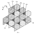
- FIG. 2 is the shape of the main sub-pixel according to the first embodiment of the present disclosure.
- FIG. 3 is the shape of the compensation sub-pixel according to the first embodiment of the present disclosure.
- FIG. 4 is a pixel structure diagram of the first embodiment of the present disclosure.
- FIG. 5 is the shape of the main sub-pixel and the compensation sub-pixel according to the second embodiment of the present disclosure.
- FIG. 6 is a schematic diagram of the arrangement of main sub-pixels and compensation sub-pixels in a second embodiment of the present disclosure.
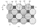
- FIG. 7 is a shape of a main sub-pixel and a compensation sub-pixel according to a third embodiment of the present disclosure.
- FIG. 8 is a schematic diagram of an arrangement of main sub-pixels and compensation sub-pixels in a third embodiment of the present disclosure.
- FIG. 9 is an implementation diagram of a compensation sub-pixel of the present disclosure.
- FIG. 10 is a diagram of another embodiment of the compensation sub-pixel of the present disclosure.
- Example 11 is a schematic diagram of a blue mask in Example 1 of the present disclosure.
- Example 12 is a schematic diagram of a red mask in Example 1 of the present disclosure.
- Example 13 is a schematic diagram of a green mask in Example 1 of the present disclosure.
- FIG. 14 is a schematic diagram of blue and red mask overlays in Example 1 of the present disclosure.
- FIG. 15 is a schematic diagram of superposition of blue, red, and green mask plates in Embodiment 1 of the present disclosure.
- FIG. 16 is a schematic diagram of a mask in Embodiment 2 of the present disclosure.
- the present disclosure provides a pixel structure, a display screen, and a metal mask.
- a pixel structure a display screen, and a metal mask.
- the present disclosure will be described in further detail below. It should be understood that the specific embodiments described herein are only used to explain the present disclosure and are not intended to limit the present disclosure.
- the present disclosure provides a preferred embodiment of a pixel structure. As shown in FIG. 1, it includes three single-color main sub-pixels 1, which are a first main sub-pixel 11, a second main sub-pixel 12, and a third main sub-pixel 13, Three types of compensation sub-pixels 2 are also included: a fourth compensation sub-pixel 24, a fifth compensation sub-pixel 25, and a sixth compensation sub-pixel 26 (refer to FIG. 4), wherein the three monochrome colors can be red, green, and blue The three colors can also be white plus any two colors of red, green, and blue.
- the three main sub-pixels constitute the basic unit of color, and the three compensation sub-pixels 2 are used to adjust the difference in the decline of different color devices. Reduce the deviation of white balance and improve the display effect.
- the main sub-pixel 1 is shown in FIG. 2 and its shape is composed of two regular pentagons with the same side length, and the sides of the two regular pentagons coincide;
- the compensation sub-pixel 2 is shown in FIG. 3 and its shape It is a rhombus whose side length is equal to that of the regular pentagon, and the acute angle of the rhombus is 36°.
- the first main sub-pixel 11 the second main sub-pixel 12 and the third main sub-pixel 13 are sequentially arranged and arrayed, and the two adjacent main sub-pixels have 2 vertices (as shown in the figure Vertex A and vertex B) coincide, and a diamond-shaped gap is formed between them, and a compensation sub-pixel 2 is provided at the diamond-shaped gap.
- one vertex of the main sub-pixel coincides with the vertex of the acute angle of the compensation sub-pixel, namely the vertex B in the figure, and the main sub-pixel and the compensation sub-pixel are in the first
- the symmetry axes in the two directions coincide; the arrangement order of all sub-pixels along the second direction b is (see FIG. 4): the first main sub-pixel 11 and the fifth compensation sub-pixel 25 are alternately arranged, and the second main sub-pixel 12 and The sixth compensation sub-pixels 26 are alternately arranged, and the third main sub-pixel 13 and the fourth compensation sub-pixel 24 are alternately arranged.
- the pixel structure of the present disclosure can be completely arrayed to form a compact close-packed array pattern.
- the unit in the dotted frame in FIG. 4 is the smallest array unit, and the pixel structure of the first embodiment of the present disclosure can be obtained by arraying this unit.
- This array method can be referred to in other embodiments of the present disclosure, which will not be described later Repeat.
- a preferred embodiment of the second pixel structure provided by the present disclosure includes three primary primary pixels 1A and three compensation sub-pixels of red, green, and blue.
- the shape of the primary sub-pixel 1A is A regular hexagon and a regular triangle are formed, the sides of the two figures have the same length and one side coincides; the shape of the compensation sub-pixel 2A is the same as the regular triangle.
- the main sub-pixel 1A includes three types, namely a first main sub-pixel 11A, a second main sub-pixel 12A, and a third main sub-pixel 13A; the three main sub-pixels (11A, 12A, 13A) are in the first In the direction a, they are sequentially arranged and arrayed; the compensation sub-pixel 2A includes three types, namely a fourth compensation sub-pixel 24A, a fifth compensation sub-pixel 25A, and a sixth compensation sub-pixel 26A.
- the first main sub The pixels 11A and the fifth compensation sub-pixels 25A are alternately arranged, the second main sub-pixel 12A and the sixth compensation sub-pixel 26A are alternately arranged, and the third main sub-pixel 13A and the fourth compensation sub-pixel 24A are alternately arranged, forming a compact close-packed array pattern.
- a preferred embodiment of the third pixel structure provided by the present disclosure includes three primary primary pixels of red, green and blue 1B and a compensation subpixel 2B, the primary subpixel 1B is a positive octagon
- the shape and the compensation sub-pixel 2B are square, and the two sides have the same side length.
- the main sub-pixel 1B includes three types, namely a first main sub-pixel 11B, a second main sub-pixel 12B, and a third main sub-pixel 13B; the three main sub-pixels (11B, 12B, 13B) are in the first In the direction a, they are sequentially arranged and arrayed; the compensation sub-pixel 2B includes three types, namely a fourth compensation sub-pixel 24B, a fifth compensation sub-pixel 25B, and a sixth compensation sub-pixel 26B.
- the first main sub The pixels 11B and the fifth compensation sub-pixel 25B are alternately arranged, the second main sub-pixel 12B and the sixth compensation sub-pixel 26B are alternately arranged, and the third main sub-pixel 13B and the fourth compensation sub-pixel 24B are alternately arranged, forming a compact close-packed array pattern.
- main sub-pixels of the present disclosure can also be designed as other polygonal structures, and corresponding compensation sub-pixels can be designed to form a close-packed structure of the array, and those skilled in the art may do so according to the above embodiments provided by the present disclosure It can be obtained by simple changes and will not be repeated in this disclosure.
- the pattern formed by the arrangement of adjacent sub-pixels of the same color is formed through an opening of the metal mask plate, which increases the opening of the mask pattern on the mask plate and improves the display
- the resolution of the screen at the same time, through the common compensation sub-pixel, the difference of the decline of the devices of different colors is adjusted to reduce the deviation of the white balance and improve the display effect.
- the present disclosure also provides a color design scheme for the compensation sub-pixel.
- at least one compensation sub-pixel has a color different from that of two main sub-pixels adjacent to the compensation sub-pixel. That is, there are three cases, which will be described with the foregoing embodiment of the first pixel structure, which specifically includes: (1) As shown in FIG. 9, the color of the fourth compensation sub-pixel 24 is different from the first main sub-pixel 11 and the second The color of the main sub-pixel 12, and the fifth compensation sub-pixel 25 and the sixth compensation sub-pixel 26 are consistent with the color of one of the adjacent main sub-pixels; (2) As shown in FIG.
- the fourth compensation sub-pixel 24 Is different from the colors of the first main subpixel 11 and the second main subpixel 12
- the fifth compensation subpixel 25 is different from the colors of the second main subpixel 12 and the third main subpixel 13
- the sixth compensation subpixel 26 is The color of one of the adjacent main sub-pixels is the same; (3) The colors of the three types of compensation sub-pixels are not consistent with the color of the main sub-pixels located adjacent to them. Please refer to FIG. 4.
- the colors of the fourth compensation sub-pixel 24, the fifth compensation sub-pixel 25, and the sixth compensation sub-pixel 26 are independently of each other: any single primary color or a mixture of two or more single primary colors
- the color is preferably red, green, blue and their mixed colors, so that the number of metal masks and processing steps can be reduced as much as possible.
- the present disclosure can design different compensation sub-pixel schemes according to actual needs to adjust the display color and resolution.
- a preferred design scheme of the compensation sub-pixel is: referring to the first direction, the color of the compensation sub-pixel is: a mixed color of two adjacent main sub-pixels.
- the color of the fourth compensation sub-pixel 24 is a mixture of colors of the first main sub-pixel 11 and the second main sub-pixel 12
- the fifth compensation sub-pixel 25 is the second main sub-pixel 12 and the third main sub-pixel
- the color mixture of 13 colors, the sixth compensation sub-pixel 26 is the color mixture of the colors of the third main sub-pixel 13 and the first main sub-pixel 11.
- the compensation sub-pixel is designed in three colors, and is the color mixture of the main sub-pixel adjacent to the compensation sub-pixel in the a direction, which minimizes the deviation of the white balance, has the best display effect, and has the fewest manufacturing processes.
- the present disclosure also provides a display screen, wherein the pixel structure in the display screen is manufactured by the above array method, and a display with high resolution and good display effect can be obtained.
- the pixel structure of the present disclosure is applied to OLED devices and can produce better display effects. This is because in current R, G, and B three-primary-color OLED devices, different light colors have different brightness decay rates, which is easy to cause the strength control of the three-primary colors during display is not easy, and the display screen has a color shift.
- the present disclosure uses a common compensation sub-pixel , Adjust the difference of the decline of different color devices, can reduce the deviation of white balance.
- the present disclosure also provides a metal mask plate including a set of graphic arrays, the array unit of the graphic array is a graphic of any combination of main sub-pixels and compensation sub-pixels in the pixel structure as described above, specifically, Taking the first embodiment of the pixel structure as an example, the combined graphics include, but are not limited to, the graphic elements in the metal masks shown in FIGS. 11, 13 and 16 in the drawings of this specification.
- Embodiment 1 (the color of only one compensation sub-pixel is different from the color of two main sub-pixels adjacent to the compensation sub-pixel)
- the array elements for version G are: main sub-pixel graphics.
- the sub-pixel 24 has a pixel structure of mixed red and blue colors.
- Embodiment 2 (the color of only one compensation sub-pixel is the same as the color of two main sub-pixels adjacent to the compensation sub-pixel, and the other two are different, for example, the fourth compensation sub-pixel 24 and the fifth compensation sub-pixel 25)
- a metal mask with the graphic unit shown in FIG. 16 as the array unit can be made.
- the graphic unit in FIG. 16 is a graphic formed by superimposing a main sub-pixel with an adjacent diamond shape.
- the specific manufacturing process and graphics overlay can refer to Embodiment 1, and will not be described in detail.
- Embodiment 3 (the color of any one kind of compensation sub-pixel is different from the colors of two main sub-pixels adjacent to the compensation sub-pixel)
- Three mask plates containing the array unit shown in FIG. 11 can be manufactured.
- the specific manufacturing process and graphics superimposition refer to Embodiment 1, which will not be described in detail.
- the present disclosure provides a pixel structure, a display screen, and a metal mask.
- the new pixel structure provided by the present disclosure allows the pattern formed by the arrangement of adjacent sub-pixels of the same color to pass through the metal during the evaporation process An opening of the mask plate is formed, which increases the opening of the mask pattern on the mask plate and improves the resolution of the display screen; at the same time, through the common compensation sub-pixel, the difference of the decline of the devices of different colors is adjusted to reduce the deviation of the white balance and improve
- the display effect is provided; the present disclosure also provides a variety of supplementary sub-pixel design solutions, which can further adjust the display color and resolution.
Landscapes
- Chemical & Material Sciences (AREA)
- Chemical Kinetics & Catalysis (AREA)
- Engineering & Computer Science (AREA)
- Materials Engineering (AREA)
- Mechanical Engineering (AREA)
- Metallurgy (AREA)
- Organic Chemistry (AREA)
- Devices For Indicating Variable Information By Combining Individual Elements (AREA)
- Electroluminescent Light Sources (AREA)
Abstract
一种像素结构、显示屏及金属掩膜版,其中,像素结构包括三种单色的主子像素(1)和三种补偿子像素(2),六种子像素在第一方向(a)以及垂直于所述第一方向(a)的第二方向(b)上按照规定的顺序排列。在蒸镀过程中,新像素结构使相邻的同色子像素排布形成的图形通过金属掩模板的一个开口形成,使掩模板上的掩模图形开口增大,提高了显示屏的分辨率;同时通过共用的补偿子像素(2),调节不同颜色器件的衰退差异,减少白色平衡的偏差,提高了显示效果。
Description
本公开涉及显示屏技术领域,尤其涉及一种像素结构、显示屏及金属掩膜版。
显示屏的彩色显示通过红(R)、绿(G)、蓝(B)三个子像素混色产生,不同颜色的子像素需使用不同颜色的材料蒸镀,像素大小和位置通过精细金属掩模板(FMM)控制。由于蒸镀工艺和材料性能的限制,FMM的蒸镀图形开口尺寸与开口间距已达到极限,FMM的制作精度已经很难再有较大提高,无法继续依靠缩小蒸镀图形开口尺寸来提高显示产品的分辨率;
因此,现有技术还有待于改进和发展。
发明内容
鉴于上述现有技术的不足,本公开的目的在于提供一种像素结构、显示屏及金属掩膜版,旨在解决现有的显示屏的分辨率无法进一步提高的问题。
本公开的技术方案如下:
一种像素结构,包括三种形状一致的单色的主子像素,分别为第一主子像素、第二主子像素和第三主子像素,还包括三种形状一致的补偿子像素,分别为第四补偿子像素、第五补偿子像素和第六补偿子像素;
在第一方向上:第一主子像素、第二主子像素和第三主子像素以设定的间隙依次排列并阵列;
垂直于所述第一方向的第二方向上:第一主子像素和第五补偿子像素交替排列,第二主子像素和第六补偿子像素交替排列,第三主子像素和第四补偿子像素交替排列。
所述的像素结构,其中,所述像素结构形成密排阵列图形。
所述的像素结构,其中,所述主子像素的形状由两个边长相同的正五边形构成,两个正 五边形的一边重合。
所述的像素结构,其中,所述补偿子像素的形状为边长与所述正五边形的边长相等的菱形,所述菱形的锐角为36°。
所述的像素结构,其中,在所述第二方向上:所述主子像素的一个顶点和所述补偿子像素的锐角的顶点重合,且所述主子像素和所述补偿子像素在所述第二方向上的对称轴重合。
所述的像素结构,其中,所述主子像素的形状由一个正六边形和一个正三角形构成,两个图形的边长相等并且一条边重合;所述补偿子像素的形状与所述正三角形相同。
所述的像素结构,其中,所述主子像素的形状为正八边形。
所述的像素结构,其中,所述补偿子像素的形状为边长与所述正六边形的边长相等的正方形。
所述的像素结构,其中,参考所述第一方向,至少有一种补偿子像素的颜色与相邻于该补偿子像素的两个主子像素的颜色不相同。
所述的像素结构,其中,所述第四补偿子像素、所述第五补偿子像素和所述第六补偿子像素的颜色相互独立地为:任意一种单原色或两种以上的单原色的混合色。
所述的像素结构,其中,参考所述第一方向,所述补偿子像素的颜色为:相邻的两个主子像素的混合色。
一种显示屏,包含如上所述的像素结构。
所述的显示屏,其中,所述显示屏为OLED显示屏。
一种金属掩膜版,包括一组图形阵列,所述图形阵列的阵列单元为如上所述的像素结构中的主子像素和补偿子像素的任意组合的图形。
有益效果:本公开提供了一种如上所述的像素结构,在蒸镀过程中,使相邻的同色子像素排布形成的图形通过金属掩模板的一个开口形成,使掩模板上的掩模图形开口增大,提高了显示屏的分辨率;同时通过共用的补偿子像素,调节不同颜色器件的衰退差异,减少白色平衡的偏差,提高了显示效果。
图1为本公开第一种实施方式的主子像素和补偿子像素的排列示意图。
图2为本公开第一种实施方式的主子像素的形状。
图3为本公开第一种实施方式的补偿子像素的形状。
图4为本公开第一种实施方式的像素结构图。
图5为本公开第二种实施方式的主子像素和补偿子像素的形状。
图6为本公开第二种实施方式的主子像素和补偿子像素的排列示意图。
图7为本公开第三种实施方式的主子像素和补偿子像素的形状。
图8为本公开第三种实施方式的主子像素和补偿子像素的排列示意图。
图9为本公开的一种补偿子像素的实施方案图。
图10为本公开的另一种补偿子像素的实施方案图。
图11为本公开实施例1中的蓝色掩膜版示意图。
图12为本公开实施例1中的红色掩膜版示意图。
图13为本公开实施例1中的绿色掩膜版示意图。
图14为本公开实施例1中的蓝色、红色掩膜版叠加示意图。
图15为本公开实施例1中的蓝色、红色、绿色掩膜版叠加示意图。
图16为本公开实施例2中的一种掩膜版示意图。
本公开提供了一种像素结构、显示屏及金属掩膜版,为使本公开的目的、技术方案及效果更加清楚、明确,以下对本公开进一步详细说明。应当理解,此处所描述的具体实施例仅仅用以解释本公开,并不用于限定本公开。
本公开提供了一种像素结构的较佳实施例,如图1所示,包括三种单色的主子像素1,分别为第一主子像素11、第二主子像素12和第三主子像素13,还包括三种补偿子像素2,分别为第四补偿子像素24、第五补偿子像素25和第六补偿子像素26(参照图4),其中,三种单色可以是红、绿、蓝三种颜色,也可以是白色加上红、绿、蓝中的任意两种颜色,三种主子像1素构成色彩的基础单元,三种补偿子像素2用于调节不同颜色器件的衰退差异,减 少白色平衡的偏差,提高显示的效果。
所述主子像素1如图2所示,其形状由两个边长相同的正五边形构成,两个正五边形的一边重合;所述补偿子像素2如图3所示,其形状为边长与所述正五边形的边长相等的菱形,所述菱形的锐角为36°。
如图1所示,在第一方向a上:第一主子像素11、第二主子像素12和第三主子像素13依次排列并阵列,相邻的两个主子像素有2个顶点(如图中顶点A和顶点B)重合,并且之间形成菱形间隙,所述菱形间隙处设置有补偿子像素2。
垂直于所述第一方向a的第二方向b上:主子像素的一个顶点和补偿子像素的锐角的顶点重合,即图中的顶点B,并且该主子像素和该补偿子像素在所述第二方向上的对称轴重合;沿所述第二方向b的所有子像素的排列顺序为(参照图4):第一主子像素11和第五补偿子像素25交替排列,第二主子像素12和第六补偿子像素26交替排列,第三主子像素13和第四补偿子像素24交替排列。根据上述规则,可以将本公开的像素结构完整阵列出来,形成紧凑的密排阵列图形。图4中虚线框内的单元为最小阵列单元,将此单元进行阵列即可得到本公开第一种实施例的像素结构,本公开其他实施例中均可以参照此阵列方法,后面不再对此进行赘述。
本公开提供的第二种像素结构的较佳实施例,如图5和图6所示,包括红、绿、蓝三种单原色的主子像素1A和补偿子像素2A,主子像素1A的形状由一个正六边形和一个正三角形构成,两个图形的边长相等并且一条边重合;补偿子像素2A的形状与所述正三角形相同。
具体的,如图6所示,主子像素1A包括三种,分别为第一主子像素11A、第二主子像素12A和第三主子像素13A;三种主子像素(11A、12A、13A)在第一方向a上,依次排列并阵列;补偿子像素2A包括三种,分别为第四补偿子像素24A、第五补偿子像素25A和第六补偿子像素26A,在第二方向b上,第一主子像素11A和第五补偿子像素25A交替排列,第二主子像素12A和第六补偿子像素26A交替排列,第三主子像素13A和第四补偿子像素24A交替排列,形成紧凑的密排阵列图形。
本公开提供的第三种像素结构的较佳实施例,如图7和图8所示,包括红、绿、蓝三种单原色的主子像素1B和补偿子像素2B,主子像素1B为正八边形,补偿子像素2B为正方形, 两者边长相等。
具体的,如图8所示,主子像素1B包括三种,分别为第一主子像素11B、第二主子像素12B和第三主子像素13B;三种主子像素(11B、12B、13B)在第一方向a上,依次排列并阵列;补偿子像素2B包括三种,分别为第四补偿子像素24B、第五补偿子像素25B和第六补偿子像素26B,在第二方向b上,第一主子像素11B和第五补偿子像素25B交替排列,第二主子像素12B和第六补偿子像素26B交替排列,第三主子像素13B和第四补偿子像素24B交替排列,形成紧凑的密排阵列图形。
需要说明的是,本公开的主子像素还可以设计为其他多边形结构,并设计相应的补偿子像素,能够形成阵列的密排结构即可,本领域技术人员可根据本公开提供的上述实施例做简单变化即可得到,本公开不再赘述。
本公开提供的新的像素结构,在蒸镀过程中,相邻的同色子像素排布形成的图形通过金属掩模板的一个开口形成,使掩模板上的掩模图形开口增大,提高了显示屏的分辨率;同时通过共用的补偿子像素,调节不同颜色器件的衰退差异,减少白色平衡的偏差,提高了显示效果。
本公开还提供了补偿子像素的颜色设计方案,参考所述第一方向,至少有一种补偿子像素的颜色与相邻于该补偿子像素的两个主子像素的颜色不相同。即存在三种情况,以前述的第一种像素结构的实施例进行说明,具体包括:(1)如图9所示,第四补偿子像素24的颜色不同于第一主子像素11和第二主子像素12的颜色,而第五补偿子像素25和第六补偿子像素26分别与位于其相邻的其中一个主子像素的颜色一致;(2)如图10所示,第四补偿子像素24的颜色不同于第一主子像素11和第二主子像素12的颜色,第五补偿子像素25不同于第二主子像素12和第三主子像素13的颜色,而第六补偿子像素26与位于其相邻的其中一个主子像素的颜色一致;(3)三种补偿子像素与位于其相邻的主子像素的颜色都不一致,可参考图4。进一步的,所述第四补偿子像素24、所述第五补偿子像素25和所述第六补偿子像素26的颜色相互独立地为:任意一种单原色或两种以上的单原色的混合色,优选为红、绿、蓝及其混合颜色,这样可以尽量减少金属掩膜版的数量以及加工工序。
可以看出,本公开可根据实际需要,设计不同的补偿子像素方案,来调节显示颜色及分 辨率。
优选的一种补偿子像素的设计方案为:参考所述第一方向,所述补偿子像素的颜色为:相邻的两个主子像素的混合色。具体地,参考图4,第四补偿子像素24的颜色为第一主子像素11和第二主子像素12的颜色的混色,第五补偿子像素25则为第二主子像素12和第三主子像素13的颜色的混色,第六补偿子像素26则为第三主子像素13和第一主子像素11的颜色的混色。本方案中,补偿子像素设计为三种颜色,并且为a方向上位于该补偿子像素相邻的主子像素的混色,最大程度地减少白色平衡的偏差,显示效果最好,而且制作工序最少。
本公开还提供了一种显示屏,其中,显示屏中的像素结构采用上述的阵列方法进行制作,可获得分辨率高、显示效果好的显示器。
本公开的像素结构应用于OLED器件中,能产生更好的显示效果。这是由于目前的R、G、B三原色OLED器件中,不同光色的亮度衰退速率不同,容易造成显示时三原色的强弱控制不易,使显示画面产生色偏,本公开通过共用的补偿子像素,调节不同颜色器件的衰退差异,可以减少白色平衡的偏差。
本公开还提供了一种金属掩膜版,包括一组图形阵列,所述图形阵列的阵列单元为如上所述的像素结构中的主子像素和补偿子像素的任意组合的图形,具体的,以第一种像素结构的实施例为例,组合的图形包括但不限于本说明书附图中的图11、图13和图16所示的金属掩膜版中的图形单元。
下面以前述的第一种实施方式的像素结构为例,结合掩膜版来具体说明像素结构的制作方法。
实施例1(只有一种补偿子像素的颜色与相邻于该补偿子像素的两个主子像素的颜色不相同)
分别制作三原色金属掩膜版B、R、G,如图11-图13所示,其中掩膜版B和R的阵列单元均为:主子像素叠加相邻的两个菱形形成的图形,掩膜版G为的阵列单元均为:主子像素图形。制作时,可以首先制作蓝色子像素,然后制作红色子像素得到图14所示的图形,最后制作绿色子像素,得到如图15所示的图形,得到主子像素为红、绿、蓝,补偿子像素24为红蓝混色的像素结构。
实施例2(只有一种补偿子像素的颜色与相邻于该补偿子像素的两个主子像素的颜色相同,另两种不相同,例如第四补偿子像素24和第五补偿子像素25)
可以制作一张以图16所示的图形单元为阵列单元的金属掩膜版,图16中的图形单元为一个主子像素叠加一个相邻的菱形形成的图形,制作二张包含图14中所示的阵列单元的掩膜版,具体制作过程及图形叠加均可参照实施例1,不再赘述。
实施例3(任一种补偿子像素的颜色与相邻于该补偿子像素的两个主子像素的颜色都不相同)
可以制作三张包含图11中所示的阵列单元的掩膜版,具体制作过程及图形叠加均可参照实施例1,不再赘述。
综上所述,本公开提供了一种像素结构、显示屏及金属掩膜版,本公开提供的新像素结构,在蒸镀过程中,使相邻的同色子像素排布形成的图形通过金属掩模板的一个开口形成,使掩模板上的掩模图形开口增大,提高了显示屏的分辨率;同时通过共用的补偿子像素,调节不同颜色器件的衰退差异,减少白色平衡的偏差,提高了显示效果;本公开还提供了多种补充子像素的设计方案,可进一步来调节显示颜色及分辨率。
应当理解的是,本公开的应用不限于上述的举例,对本领域普通技术人员来说,可以根据上述说明加以改进或变换,所有这些改进和变换都应属于本公开所附权利要求的保护范围。
Claims (20)
- 一种像素结构,其特征在于,包括三种形状一致的单色的主子像素,分别为第一主子像素、第二主子像素和第三主子像素,还包括三种形状一致的补偿子像素,分别为第四补偿子像素、第五补偿子像素和第六补偿子像素;在第一方向上:第一主子像素、第二主子像素和第三主子像素以设定的间隙依次排列并阵列;垂直于所述第一方向的第二方向上:第一主子像素和第五补偿子像素交替排列,第二主子像素和第六补偿子像素交替排列,第三主子像素和第四补偿子像素交替排列。
- 根据权利要求1所述的像素结构,其特征在于,所述像素结构形成密排阵列图形。
- 根据权利要求1所述的像素结构,其特征在于,所述三种形状一致的单色的主子像素的颜色为红、绿、蓝,或者白色加上红、绿、蓝中的任意两种颜色。
- 根据权利要求1所述的像素结构,其特征在于,所述主子像素的形状由两个边长相同的正五边形构成,两个正五边形的一边重合。
- 根据权利要求4所述的像素结构,其特征在于,所述补偿子像素的形状为边长与所述正五边形的边长相等的菱形。
- 根据权利要求5所述的像素结构,其特征在于,所述菱形的锐角为36°。
- 根据权利要求5所述的像素结构,其特征在于,在所述第二方向上:所述主子像素的一个顶点和所述补偿子像素的锐角的顶点重合。
- 根据权利要求5所述的像素结构,其特征在于,在所述第二方向上:所述主子像素和所述补偿子像素在所述第二方向上的对称轴重合。
- 根据权利要求1所述的像素结构,其特征在于,所述主子像素的形状由一个正六边形和一个正三角形构成,两个图形的边长相等并且一条边重合。
- 根据权利要求9所述的像素结构,其特征在于,所述补偿子像素的形状与所述正三角形相同。
- 根据权利要求1所述的像素结构,其特征在于,所述主子像素的形状为正八边形。
- 根据权利要求11所述的像素结构,其特征在于,所述补偿子像素的形状为边长 与所述正八边形的边长相等的正方形。
- 根据权利要求1所述的像素结构,其特征在于,参考所述第一方向,至少有一种补偿子像素的颜色与相邻于该补偿子像素的两个主子像素的颜色不相同。
- 根据权利要求13所述的像素结构,其特征在于,所述第四补偿子像素、所述第五补偿子像素和所述第六补偿子像素的颜色相互独立地为:任意一种单原色或两种以上的单原色的混合色。
- 根据权利要求14所述的像素结构,其特征在于,所述单原色为红、绿、蓝。
- 根据权利要求14所述的像素结构,其特征在于,参考所述第一方向,所述补偿子像素的颜色为:相邻的两个主子像素的混合色。
- 根据权利要求1所述的像素结构,其特征在于,相邻的同色子像素排布形成的图形通过金属掩模板的一个开口形成。
- 一种显示屏,其特征在于,包含权利要求1-17任一所述的像素结构。
- 根据权利要求18所述的显示屏,其特征在于,所述显示屏为OLED显示屏。
- 一种金属掩膜版,包括一组图形阵列,其特征在于,所述图形阵列的阵列单元为权利要求1-17任一所述的像素结构中的主子像素和补偿子像素的任意组合的图形。
Applications Claiming Priority (2)
| Application Number | Priority Date | Filing Date | Title |
|---|---|---|---|
| CN201811643518.1A CN111384093B (zh) | 2018-12-30 | 2018-12-30 | 一种像素结构、显示屏及金属掩膜版 |
| CN201811643518.1 | 2018-12-30 |
Publications (1)
| Publication Number | Publication Date |
|---|---|
| WO2020140494A1 true WO2020140494A1 (zh) | 2020-07-09 |
Family
ID=71218249
Family Applications (1)
| Application Number | Title | Priority Date | Filing Date |
|---|---|---|---|
| PCT/CN2019/108326 Ceased WO2020140494A1 (zh) | 2018-12-30 | 2019-09-27 | 一种像素结构、显示屏及金属掩模板 |
Country Status (2)
| Country | Link |
|---|---|
| CN (1) | CN111384093B (zh) |
| WO (1) | WO2020140494A1 (zh) |
Cited By (1)
| Publication number | Priority date | Publication date | Assignee | Title |
|---|---|---|---|---|
| CN114335113A (zh) * | 2021-12-30 | 2022-04-12 | 京东方科技集团股份有限公司 | 一种显示面板、显示装置和掩膜板组合结构 |
Citations (5)
| Publication number | Priority date | Publication date | Assignee | Title |
|---|---|---|---|---|
| US20060033422A1 (en) * | 2004-08-10 | 2006-02-16 | Industrial Technology Research Institute | Full-color organic electroluminescence display |
| CN103576366A (zh) * | 2013-11-15 | 2014-02-12 | 北京京东方光电科技有限公司 | 显示面板及其显示方法、显示装置 |
| CN104681594A (zh) * | 2015-03-11 | 2015-06-03 | 京东方科技集团股份有限公司 | 像素排列结构和显示装置 |
| CN108538884A (zh) * | 2017-03-02 | 2018-09-14 | 三星显示有限公司 | 有机发光显示装置 |
| CN109037287A (zh) * | 2018-07-27 | 2018-12-18 | 京东方科技集团股份有限公司 | 子像素排列结构、掩膜装置、显示面板及显示装置 |
Family Cites Families (2)
| Publication number | Priority date | Publication date | Assignee | Title |
|---|---|---|---|---|
| CN103544901B (zh) * | 2013-11-15 | 2016-04-13 | 北京京东方光电科技有限公司 | 显示面板及其显示方法、显示装置 |
| CN105762169A (zh) * | 2014-12-17 | 2016-07-13 | 上海和辉光电有限公司 | Oled像素排列结构以及像素排列结构的蒸镀掩膜 |
-
2018
- 2018-12-30 CN CN201811643518.1A patent/CN111384093B/zh active Active
-
2019
- 2019-09-27 WO PCT/CN2019/108326 patent/WO2020140494A1/zh not_active Ceased
Patent Citations (5)
| Publication number | Priority date | Publication date | Assignee | Title |
|---|---|---|---|---|
| US20060033422A1 (en) * | 2004-08-10 | 2006-02-16 | Industrial Technology Research Institute | Full-color organic electroluminescence display |
| CN103576366A (zh) * | 2013-11-15 | 2014-02-12 | 北京京东方光电科技有限公司 | 显示面板及其显示方法、显示装置 |
| CN104681594A (zh) * | 2015-03-11 | 2015-06-03 | 京东方科技集团股份有限公司 | 像素排列结构和显示装置 |
| CN108538884A (zh) * | 2017-03-02 | 2018-09-14 | 三星显示有限公司 | 有机发光显示装置 |
| CN109037287A (zh) * | 2018-07-27 | 2018-12-18 | 京东方科技集团股份有限公司 | 子像素排列结构、掩膜装置、显示面板及显示装置 |
Cited By (1)
| Publication number | Priority date | Publication date | Assignee | Title |
|---|---|---|---|---|
| CN114335113A (zh) * | 2021-12-30 | 2022-04-12 | 京东方科技集团股份有限公司 | 一种显示面板、显示装置和掩膜板组合结构 |
Also Published As
| Publication number | Publication date |
|---|---|
| CN111384093B (zh) | 2023-05-12 |
| CN111384093A (zh) | 2020-07-07 |
Similar Documents
| Publication | Publication Date | Title |
|---|---|---|
| CN113990912B (zh) | 像素排列结构、显示基板以及显示装置 | |
| JP6759396B2 (ja) | ピクセル構造およびその表示方法、表示装置 | |
| TWI555195B (zh) | 顯示器的畫素排列結構 | |
| JP6657127B2 (ja) | 画素構造、その表示方法、及び表示装置 | |
| TWI780694B (zh) | 像素排布結構、顯示面板及顯示裝置 | |
| JP6752156B2 (ja) | 画素構造、その表示方法、及び関連表示装置 | |
| CN110133919B (zh) | 显示基板和显示装置 | |
| US9647039B1 (en) | Array substrate, display panel, display device, and fabrication method thereof | |
| TWI679759B (zh) | 圖元結構及採用該圖元結構的有機發光顯示器 | |
| CN108155204B (zh) | 一种像素排列结构、显示装置及掩膜板 | |
| WO2020124693A1 (zh) | Oled像素结构 | |
| US20170352710A1 (en) | Oled pixel arrangement structure and display device | |
| US11882748B2 (en) | Pixel structure and display panel | |
| CN104766563B (zh) | 一种像素结构及显示面板和显示装置 | |
| CN107086239A (zh) | 像素结构及其制备方法和显示装置 | |
| WO2018223475A1 (zh) | Oled显示面板的像素排列结构及oled显示面板 | |
| CN112436031A (zh) | 像素排布结构、显示面板及显示装置 | |
| CN104201192A (zh) | 显示屏的像素结构、金属掩模板及oled显示屏 | |
| CN206194742U (zh) | 一种像素排列结构、显示装置及掩膜板 | |
| CN105355643B (zh) | 一种像素结构、其制作方法、显示面板及显示装置 | |
| CN105789261A (zh) | 像素阵列及其制造方法和有机发光二极管阵列基板 | |
| CN108598141B (zh) | 一种像素显示模组以及制作像素显示模组的掩膜板 | |
| JP2020509415A (ja) | 画素構造、マスク及び表示デバイス | |
| WO2016141659A1 (zh) | 像素排列结构和显示装置 | |
| US20200194512A1 (en) | Organic light-emitting diode pixel structure |
Legal Events
| Date | Code | Title | Description |
|---|---|---|---|
| 121 | Ep: the epo has been informed by wipo that ep was designated in this application |
Ref document number: 19907277 Country of ref document: EP Kind code of ref document: A1 |
|
| NENP | Non-entry into the national phase |
Ref country code: DE |
|
| 122 | Ep: pct application non-entry in european phase |
Ref document number: 19907277 Country of ref document: EP Kind code of ref document: A1 |