WO2020137495A1 - 液晶表示素子 - Google Patents
液晶表示素子 Download PDFInfo
- Publication number
- WO2020137495A1 WO2020137495A1 PCT/JP2019/048139 JP2019048139W WO2020137495A1 WO 2020137495 A1 WO2020137495 A1 WO 2020137495A1 JP 2019048139 W JP2019048139 W JP 2019048139W WO 2020137495 A1 WO2020137495 A1 WO 2020137495A1
- Authority
- WO
- WIPO (PCT)
- Prior art keywords
- liquid crystal
- region
- trunk portion
- substrate
- trunk
- Prior art date
- Legal status (The legal status is an assumption and is not a legal conclusion. Google has not performed a legal analysis and makes no representation as to the accuracy of the status listed.)
- Ceased
Links
Images




Classifications
-
- G—PHYSICS
- G02—OPTICS
- G02F—OPTICAL DEVICES OR ARRANGEMENTS FOR THE CONTROL OF LIGHT BY MODIFICATION OF THE OPTICAL PROPERTIES OF THE MEDIA OF THE ELEMENTS INVOLVED THEREIN; NON-LINEAR OPTICS; FREQUENCY-CHANGING OF LIGHT; OPTICAL LOGIC ELEMENTS; OPTICAL ANALOGUE/DIGITAL CONVERTERS
- G02F1/00—Devices or arrangements for the control of the intensity, colour, phase, polarisation or direction of light arriving from an independent light source, e.g. switching, gating or modulating; Non-linear optics
- G02F1/01—Devices or arrangements for the control of the intensity, colour, phase, polarisation or direction of light arriving from an independent light source, e.g. switching, gating or modulating; Non-linear optics for the control of the intensity, phase, polarisation or colour
- G02F1/13—Devices or arrangements for the control of the intensity, colour, phase, polarisation or direction of light arriving from an independent light source, e.g. switching, gating or modulating; Non-linear optics for the control of the intensity, phase, polarisation or colour based on liquid crystals, e.g. single liquid crystal display cells
- G02F1/133—Constructional arrangements; Operation of liquid crystal cells; Circuit arrangements
- G02F1/1333—Constructional arrangements; Manufacturing methods
- G02F1/1337—Surface-induced orientation of the liquid crystal molecules, e.g. by alignment layers
-
- G—PHYSICS
- G02—OPTICS
- G02F—OPTICAL DEVICES OR ARRANGEMENTS FOR THE CONTROL OF LIGHT BY MODIFICATION OF THE OPTICAL PROPERTIES OF THE MEDIA OF THE ELEMENTS INVOLVED THEREIN; NON-LINEAR OPTICS; FREQUENCY-CHANGING OF LIGHT; OPTICAL LOGIC ELEMENTS; OPTICAL ANALOGUE/DIGITAL CONVERTERS
- G02F1/00—Devices or arrangements for the control of the intensity, colour, phase, polarisation or direction of light arriving from an independent light source, e.g. switching, gating or modulating; Non-linear optics
- G02F1/01—Devices or arrangements for the control of the intensity, colour, phase, polarisation or direction of light arriving from an independent light source, e.g. switching, gating or modulating; Non-linear optics for the control of the intensity, phase, polarisation or colour
- G02F1/13—Devices or arrangements for the control of the intensity, colour, phase, polarisation or direction of light arriving from an independent light source, e.g. switching, gating or modulating; Non-linear optics for the control of the intensity, phase, polarisation or colour based on liquid crystals, e.g. single liquid crystal display cells
- G02F1/133—Constructional arrangements; Operation of liquid crystal cells; Circuit arrangements
- G02F1/1333—Constructional arrangements; Manufacturing methods
- G02F1/1343—Electrodes
-
- G—PHYSICS
- G02—OPTICS
- G02F—OPTICAL DEVICES OR ARRANGEMENTS FOR THE CONTROL OF LIGHT BY MODIFICATION OF THE OPTICAL PROPERTIES OF THE MEDIA OF THE ELEMENTS INVOLVED THEREIN; NON-LINEAR OPTICS; FREQUENCY-CHANGING OF LIGHT; OPTICAL LOGIC ELEMENTS; OPTICAL ANALOGUE/DIGITAL CONVERTERS
- G02F1/00—Devices or arrangements for the control of the intensity, colour, phase, polarisation or direction of light arriving from an independent light source, e.g. switching, gating or modulating; Non-linear optics
- G02F1/01—Devices or arrangements for the control of the intensity, colour, phase, polarisation or direction of light arriving from an independent light source, e.g. switching, gating or modulating; Non-linear optics for the control of the intensity, phase, polarisation or colour
- G02F1/13—Devices or arrangements for the control of the intensity, colour, phase, polarisation or direction of light arriving from an independent light source, e.g. switching, gating or modulating; Non-linear optics for the control of the intensity, phase, polarisation or colour based on liquid crystals, e.g. single liquid crystal display cells
- G02F1/133—Constructional arrangements; Operation of liquid crystal cells; Circuit arrangements
- G02F1/136—Liquid crystal cells structurally associated with a semi-conducting layer or substrate, e.g. cells forming part of an integrated circuit
- G02F1/1362—Active matrix addressed cells
- G02F1/1368—Active matrix addressed cells in which the switching element is a three-electrode device
Definitions
- the present invention relates to a liquid crystal display device.
- MVA Multi-domain Vertical Alignment
- PSA Polymer-Sustained Alignment
- a pixel electrode having a so-called fishbone structure is used as the pixel electrode (for example, Patent Document 1).
- the fishbone structure is composed of a cross-shaped trunk portion and branch portions extending from the trunk portion, and branch portions having different extending directions are provided in each of four regions defined by the trunk portion. As a result, four liquid crystal domains having different director orientations of liquid crystal molecules are formed corresponding to the four regions.
- the orientation of the liquid crystal molecules on the trunk portion overlaps with the absorption axis of the polarizing plate, so that the area where the trunk portion is provided does not transmit light, and the cross shape corresponding to the trunk portion is formed.
- the dark line of (3) occurs in the pixel of the liquid crystal display element (the light transmittance decreases).
- liquid crystal display elements are required to have further improved transmittance, and it is necessary to improve such a decrease in transmittance.
- the size of the unit pixel becomes smaller as the pixel becomes finer, the number of trunks occupying per unit pixel increases, so that the problem of a decrease in transmittance accompanied by the occurrence of a dark line becomes remarkable.
- the pixel electrode having the conventional fishbone structure used in the PSA type liquid crystal display element it is premised that the four liquid crystal domains are formed by forming the trunk portion into a cross shape, so that the design of the trunk portion can be freely changed. The degree is small. As a result, it is not easy to improve the transmittance from the viewpoint of the structure of the pixel electrode used in the PSA liquid crystal display element.
- an object of the present invention is to freely arrange the trunk portion in the pixel electrode applicable to the PSA type liquid crystal display element.
- One aspect of the present invention is a liquid crystal display element including a first substrate, a plurality of pixel electrodes provided on the first substrate, a liquid crystal layer containing liquid crystal molecules, and a second substrate in this order.
- the pixel electrode includes a first region, a second region, a third region, and a fourth region for inclining liquid crystal molecules in different directions, and the first region, the second region, and the The region 3 and the fourth region are arranged in this order in one direction, and the pixel electrode includes a first trunk portion extending in the one direction along the first region and the second region, A second trunk portion extending in the one direction along the third region and the fourth region, and a plurality of second trunk portions that extend in the first region from the first trunk portion in a predetermined direction in substantially parallel to each other.
- the liquid crystal display element has an angle formed by the extending direction of the fourth branch portion of about 90°.
- the pixel electrode of this liquid crystal display element four regions for inclining liquid crystal molecules in different directions are arranged in one direction.
- branch portions extending in a predetermined direction are provided, and the extending direction of the first branch portion in the first region and the second branch portion in the second region are provided.
- the angle formed by the extending direction is approximately 90°
- the angle formed by the extending direction of the third branch portion in the third region and the extending direction of the fourth branch portion in the fourth region is approximately 90. °.
- this pixel electrode does not need to be provided in the shape of a cross in the center of the pixel, and may be provided at the end of the pixel, for example.
- this pixel electrode is a pixel electrode applicable to the PSA type liquid crystal display element and enables the trunk portion to be freely arranged.
- the pixel electrode is connected to the first trunk portion, is connected to the second trunk portion, and is connected to the third trunk portion provided so as to separate the first region and the second region from each other. And a fourth trunk portion provided so as to separate the four regions from each other.
- branch portions extending substantially parallel to the first to fourth branch portions can be provided from the third trunk portion and the fourth trunk portion, respectively.
- a pixel electrode capable of forming two liquid crystal domains more suitably can be obtained.
- At least a part of the first trunk portion and the second trunk portion is positioned so as not to overlap the opening of the pixel corresponding to the pixel electrode. It may be provided. In this case, since at least a part of the trunk portion that causes the generation of dark lines and the decrease in transmittance does not overlap the opening portion, the light transmission region in the unit pixel becomes wider, and the occurrence of dark lines is suppressed and the transmittance is improved. It will be possible.
- all of the first trunk portion and the second trunk portion are provided at positions that do not overlap with the opening of the pixel corresponding to the pixel electrode. You can stay. In this case, since all of the trunks that cause the generation of dark lines and the decrease in transmittance do not overlap with the openings, the light transmission area in the unit pixel is further widened, and the generation of dark lines is further suppressed and the transmittance is further improved. It becomes possible to improve.
- the planar shape of the unit pixel corresponding to the pixel electrode is a rectangle that is long in the one direction, and the length of the rectangular shape in the longitudinal direction is long. May be 1.5 times or more the length in the lateral direction.
- the lengths of the first trunk portion and the second trunk portion extending in the arrangement direction of the first to fourth regions also become long, and the area ratio of the first trunk portion and the second trunk portion in the unit pixel also becomes large. Therefore, for example, when the first trunk portion and the second trunk portion are arranged so as not to overlap the opening portion, the effects of suppressing the generation of dark lines and improving the transmittance become remarkable.
- the liquid crystal display device may further include a Cs electrode provided on the first substrate, and when viewed from the stacking direction of the first substrate, the liquid crystal layer and the second substrate, the first trunk portion and the second At least a part of the trunk portion of the C may be provided at a position overlapping with the Cs electrode.
- the first trunk portion and the second trunk portion which cause dark lines and decrease in transmittance
- the Cs electrode which may cause dark lines and decrease in transmittance
- a region that does not transmit light is narrowed (a region that transmits light is widened), and as a result, it is possible to suppress the generation of dark lines and improve the transmittance.
- the pixel electrode includes a first auxiliary branch portion extending in a direction substantially symmetrical to the extending direction of the first branch portion with respect to the first trunk portion, and a second branch portion with respect to the first trunk portion.
- a second auxiliary branch extending in a direction substantially symmetrical to the extending direction
- a third auxiliary branch extending in a direction substantially symmetrical to the extending direction of the third branch with respect to the second trunk.
- a supplementary branch portion extending in a direction substantially symmetrical to the extending direction of the fourth branch portion with respect to the second trunk portion.
- the fourth auxiliary branch portion extending in a direction substantially symmetrical to the extending direction of the first to fourth branch portions stabilizes the alignment of liquid crystal molecules near the first trunk portion or the second trunk portion. Can be made.
- the liquid crystal display element may be a PSA type liquid crystal display element.
- the alignment film may not be disposed between the liquid crystal layer and the first substrate and between the liquid crystal layer and the second substrate.
- the trunk can be freely arranged in the pixel electrode applicable to the PSA liquid crystal display element.
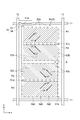
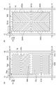
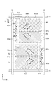
- FIG. 3 is a plan view for explaining the function and effect of the pixel electrode of FIG. 2. It is a top view which shows other one Embodiment of a pixel electrode. It is a top view which shows other one Embodiment of a pixel electrode. It is a top view which shows other one Embodiment of a pixel electrode. It is a top view which shows other one Embodiment of a pixel electrode. It is a top view which shows other one Embodiment of a pixel electrode.
- the term “abbreviated” allows for manufacturing and design errors. “About orthogonal”, “substantially perpendicular”, and “about 90°” mean that the error from 90° is within a range of ⁇ 10°, preferably within a range of ⁇ 6°, and more preferably within ⁇ 2°. It may be within the range and similar expressions for angles other than 90° may be the same.
- the terms “substantially symmetric” and “substantially parallel” mean that the errors from the angles formed with respect to the symmetry axis and the parallel axis are, for example, within ⁇ 5°, preferably within ⁇ 3°, and more preferably within ⁇ 1°. It may be in the range of °.
- FIG. 1 is an exploded perspective view showing an embodiment of a liquid crystal display element.
- a liquid crystal display element 1 according to an embodiment includes a first substrate 2, a second substrate 3, and a liquid crystal provided between the first substrate 2 and the second substrate 3. And layer 4.
- the liquid crystal layer 4 contains liquid crystal molecules 4a.
- the liquid crystal display element 1 is, for example, a PSA type liquid crystal display element.
- a plurality of pixel electrodes 5 are formed on the surface of the first substrate 2 on the liquid crystal layer 4 side.
- the liquid crystal display element 1 is a PSA type liquid crystal display element
- a polymer layer for aligning the liquid crystal molecules 4a is provided so as to cover the first substrate 2 and the plurality of pixel electrodes 5 (not shown).
- the common electrode 6 is arranged on the liquid crystal layer 4 side of the second substrate 3 (between the second substrate 3 and the liquid crystal layer 4 ).
- a color filter substrate 7 is arranged between the second substrate 3 and the common electrode 6.
- a first polarizing plate 8 is arranged on the side of the first substrate 2 opposite to the liquid crystal layer 4.
- a second polarizing plate 9 is arranged on the side of the second substrate 3 opposite to the liquid crystal layer 4.
- the first polarizing plate 8 and the second polarizing plate 9 constitute a pair of polarizing plates.
- the liquid crystal display element 1 includes a first polarizing plate 8, a first substrate 2, a pixel electrode 5, a liquid crystal layer 4, a common electrode 6, a color filter substrate 7, and a first electrode.
- the second substrate 3 and the second polarizing plate 9 are provided in this order.
- the first substrate 2 and the second substrate 3 are made of glass or resin, for example. At least one of the first substrate 2 and the second substrate 3 is made of a transparent material, and the other may be made of a transparent material, and is made of an opaque material such as metal or silicon. Good.
- the first substrate 2 and the second substrate 3 are bonded to each other by a sealing material and a sealing material such as an epoxy thermosetting composition arranged in the peripheral area, and the distance between the substrates is maintained between them. Therefore, for example, granular spacers such as glass particles, plastic particles, and alumina particles, or spacer columns made of a resin formed by a photolithography method may be arranged.
- the liquid crystal layer 4 contains a liquid crystal composition containing liquid crystal molecules 4a. Note that, in FIG. 1, the liquid crystal molecules 4 a are illustrated only in a part of the liquid crystal layer 4 for simplification, but the liquid crystal molecules 4 a are present over the entire liquid crystal layer 4.
- the liquid crystal composition contained in the liquid crystal layer 4 is, for example, a so-called n-type liquid crystal composition having a negative value of dielectric anisotropy ( ⁇ ).
- the n-type liquid crystal composition contains at least one compound (liquid crystal molecule) having a negative dielectric anisotropy, or two or more compounds.
- the compound having a negative dielectric anisotropy means a compound having a negative ⁇ sign and an absolute value larger than 2.
- ⁇ of the compound is a value extrapolated from the measured value of the dielectric anisotropy of the composition obtained by adding the compound to the liquid crystal composition for evaluation at 20°C.
- the compound having a negative dielectric anisotropy is not particularly limited, but may be, for example, one of the general formulas (N-01), (N-02), (N-03), (N-04) and (N-05). It can be a compound selected from the group of represented compounds.
- R 21 and R 22 are each independently, an alkyl group having 1 to 8 carbon atoms, an alkoxy group having 1 to 8 carbon atoms, an alkenyl group having 2 to 8 carbon atoms, or 2 carbon atoms.
- Z 8 represent alkenyloxy groups
- Z 1's each independently represent a single bond, —CH 2 CH 2 —, —OCH 2 — or —CH 2 O—
- m are each independently 1 Or represents 2.
- Examples of the compound represented by the general formula (N-01) include general formula (N-01-1), general formula (N-01-2), general formula (N-01-3) and general formula (N-01). Examples include compounds selected from the group of compounds represented by -01-4). (In the formula, R 21's each independently represent an alkyl group having 1 to 5 carbon atoms, and R 23's each independently represent an alkoxy group having 1 to 4 carbon atoms.)
- Examples of the compound represented by the general formula (N-02) include compounds represented by the general formula (N-02-1), the general formula (N-02-2), and the general formula (N-02-3). A compound selected from the group of compounds may be mentioned.
- R 21's each independently represent an alkyl group having 1 to 5 carbon atoms
- R 23's each independently represent an alkoxy group having 1 to 4 carbon atoms.
- Examples of the compound represented by the general formula (N-03) include compounds represented by the general formula (N-03-1). (In the formula, R 21 represents an alkyl group having 1 to 5 carbon atoms, and R 23 represents an alkoxy group having 1 to 4 carbon atoms.)
- Examples of the compound represented by the general formula (N-04) include compounds represented by the general formula (N-04-1). (In the formula, R 21 represents an alkyl group having 1 to 5 carbon atoms, and R 23 represents an alkoxy group having 1 to 4 carbon atoms.)
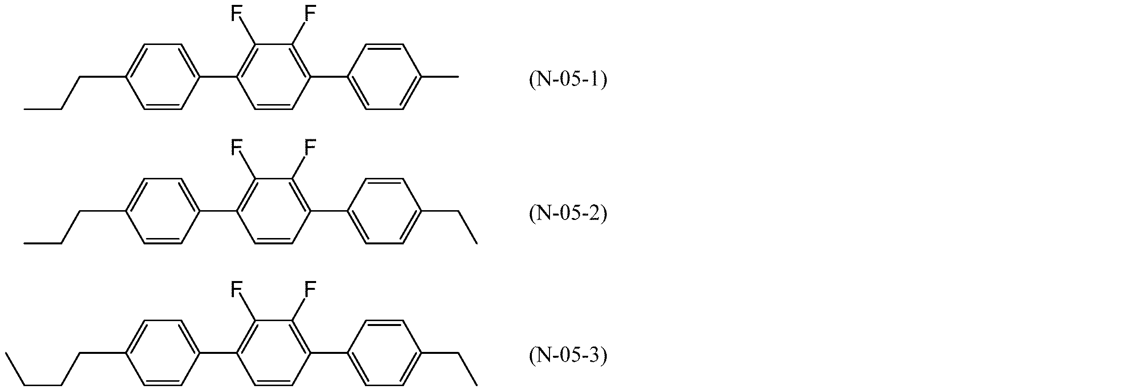
- Examples of the compound represented by the general formula (N-05) include compounds represented by the general formula (N-05-1) to the general formula (N-05-3).
- the liquid crystal composition may further contain one or more kinds of dielectrically neutral compounds.
- the dielectrically neutral compound is a compound having a value of ⁇ greater than ⁇ 2 and less than 2.
- the dielectrically neutral compound is not particularly limited, but examples thereof include compounds selected from the group of compounds represented by the general formula (NU-01) to the general formula (NU-08).
- R NU11, R NU12, R NU21, R NU22, R NU31, R NU32, R NU41, R NU42, R NU51, R NU52, R NU61, R NU62, R NU71, R NU72, R NU81 and R NU82 each independently represents an alkyl group having 1 to 8 carbon atoms, an alkoxy group having 1 to 8 carbon atoms, an alkenyl group having 2 to 8 carbon atoms or an alkenyloxy group having 2 to 8 carbon atoms. .
- the liquid crystal composition may contain one kind or two or more kinds of polymerizable compounds in addition to the above compounds. Since a liquid crystal composition containing a polymerizable compound can obtain a good alignment state by polymerization of the polymerizable compound, a PSA type, PSVA type, NPS type liquid crystal display device or a PI-less type liquid crystal having no alignment film. It is suitable for display devices.
- Examples of the polymerizable compound include compounds selected from the group consisting of compounds represented by the following general formula (RM) or general formula (RM-13). These may be used alone or in combination of two or more.
- RM general formula
- R 101 , R 102 , R 103 , R 104 , R 105 , R 106 , R 107 and R 108 are each independently P 13 -S 13 -, a carbon atom which may be substituted with a fluorine atom.
- P 3 and P 4 are each independently a formula (PG-1) to a formula (PG-5) Represents a polymerizable group represented by S 3 , S 3 represents a single bond or an alkylene group having 1 to 5 carbon atoms, and Y 1 to Y 12 each independently represent a fluorine atom or a hydrogen atom. Represents a fluorine atom.
- the polymerizable compound may be used singly or in combination of two or more, and the content of the liquid crystal composition alone or the total content of two or more is 0.1% by mass or more and 0.6% by mass or less. It is preferable to adjust within the range. Further, the content of the polymerizable compound represented by the general formula (RM) or the general formula (RM-13) in the liquid crystal composition is adjusted in the range of 0.1% by mass or more and 0.6% by mass or less. It is preferable.
- the liquid crystal composition may contain one kind or two or more kinds of alignment aids.
- the alignment aid is a compound having a function of spontaneously aligning liquid crystal molecules.
- a liquid crystal composition containing an alignment aid allows liquid crystal molecules to be aligned without an alignment film, and is therefore suitable for a PI-less type liquid crystal display device having no alignment film.
- the alignment aid has a function of spontaneously aligning liquid crystal molecules
- the alignment aid spontaneously aligning liquid crystal molecules
- the alignment aid is in direct contact with the liquid crystal layer composed of the liquid crystal composition (electrode (for example, ITO), substrate (eg, glass substrate, acrylic substrate, transparent substrate, flexible substrate, etc.), resin layer (eg, color filter substrate, alignment film, overcoat layer, etc.), insulating film (eg, inorganic material film, SiNx, etc.) )), and has a function of inducing homeotropic alignment of liquid crystal molecules contained in the liquid crystal layer.
- the liquid crystal composition electrode (for example, ITO), substrate (eg, glass substrate, acrylic substrate, transparent substrate, flexible substrate, etc.), resin layer (eg, color filter substrate, alignment film, overcoat layer, etc.), insulating film (eg, inorganic material film, SiNx, etc.) )
- ITO liquid crystal composition
- substrate eg, glass substrate, acrylic substrate, transparent substrate, flexible substrate, etc.
- the alignment aid induces alignment of the liquid crystal molecules, a polymerizable group for polymerization, a mesogenic group similar to the liquid crystal molecules, an adsorption group (polar group) capable of interacting with a member that directly contacts the liquid crystal layer. It is preferable to have an orientation-inducing group.
- the adsorption group and orientation-inducing group are preferably bonded to the mesogenic group. Further, the polymerizable group is preferably substituted on the mesogen group, the adsorbing group and the orientation inducing group directly or via a spacer group as the case requires.
- the orientation-inducing group in the orientation aid has a function of inducing the orientation of liquid crystal molecules.
- Examples of the orientation-inducing group include groups represented by general formula (AK) shown below.
- One or two or more hydrogen atoms of may be each independently substituted with a halogeno group, where * represents a bond).
- P AP1 -Sp AP1 - is preferably represented by.
- P AP1 is preferably a group selected from the group represented by general formulas (AP-1) to (AP-9) shown below.
- R AP1 and R AP2 each independently represent a hydrogen atom, an alkyl group having 1 to 5 carbon atoms or a halogenated alkyl group having 1 to 10 carbon atoms. Or two or more —CH 2 — may be substituted with —O— or —CO—, and one or more hydrogen atoms in the alkyl group are independently a halogen atom or a hydroxyl group.
- W AP1 represents a single bond, —O—, —COO— or —CH 2 — and t AP1 represents 0, 1 or 2. * in the formula represents a bond. .
- Sp AP1 is preferably a single bond or a linear or branched alkylene group having 1 to 20 carbon atoms, a single bond or a straight It is more preferably a chain alkylene group having 1 to 20 carbon atoms, and further preferably a single bond or a straight chain alkylene group having 2 to 10 carbon atoms.
- one or two or more non-adjacent —CH 2 — in the alkylene group are each independently —CH ⁇ CH—, —C ⁇ C—, —O—, —CO—, It may be substituted with —COO— or —OCO—.
- the number of polymerizable groups is preferably 1 or more and 5 or less, more preferably 1 or more and 4 or less, and further preferably 2 or more and 4 or less. Particularly preferred is 2 or 3, and most preferred is 2.
- the hydrogen atom in P AP1- Sp AP1- may be substituted with a polymerizable group, an adsorptive group and/or an orientation-inducing group.
- Polymerizable group (P AP1 -Sp AP1 -) the polymerizable group, mesogen group may be bonded to an adsorptive group and / or orientation-induced group.
- the polymerizable group (P AP1 -Sp AP1 -) is preferably binding to the mesogenic groups, the adsorption group or orientation-induced group, and more preferably binding to the mesogenic groups or adsorptive groups.
- the mesogenic group in the orientation aid means a group having a rigid portion, for example, a group having at least one cyclic group, preferably a group having 2 to 4 cyclic groups, and a cyclic group. A group having 3 to 4 is more preferable.
- the cyclic group may be linked by a linking group.
- the mesogen group preferably has a skeleton similar to that of liquid crystal molecules (liquid crystal compound) used in the liquid crystal layer.
- the “cyclic group” refers to an atomic group in which constituent atoms are cyclically bonded, and includes a carbocycle, a heterocycle, a saturated or unsaturated cyclic structure, a monocyclic, bicyclic structure, and a polycyclic group. Includes structures, aromatics, non-aromatics, etc.
- the cyclic group may contain at least one hetero atom, and may be further substituted with at least one substituent (halogeno group, polymerizable group, organic group (alkyl, alkoxy, aryl etc.).
- substituent halogeno group, polymerizable group, organic group (alkyl, alkoxy, aryl etc.).
- the mesogenic group preferably contains two or more monocycles.
- the mesogen group is preferably represented by, for example, general formula (AL).
- One or two or more non-adjacent —CH 2 — in the alkylene group may be substituted with —O—, —COO— or —OCO—, and A AL1 and A AL2 are each independently 2 Represents one or more hydrogen atoms in Z AL1 , A AL1 and A AL2 each independently represents a halogeno group, an adsorbing group, P AP1 —Sp AP1 — or a monovalent group. When a plurality of Z AL1 and A AL1 are present in the molecule, they may be the same or different, and m AL1 represents an integer of 1 to 5. * Indicates a bond.)
- the adsorptive group in the alignment aid is a group having a role of adsorbing with an adsorbent which is a layer in contact with the liquid crystal composition such as a substrate, a film and an electrode.
- the adsorption may be chemical adsorption in which a chemical bond (covalent bond, ionic bond or metal bond) is formed between the adsorbent and the adsorbate, or physical adsorption other than chemical adsorption. Good, but physical adsorption is preferred.
- Examples of the adsorptive group include groups represented by general formula (AT) shown below. (In the formula (AT), Sp AT1 represents a single bond or a linear or branched alkylene group having 1 to 25 carbon atoms.
- a hydrogen atom in the alkylene group is —OH, —CN, — It may be substituted with W AT1 —Z AT1 or P AP1 —Sp AP1 —, and —CH 2 — in the alkylene group is a cyclic group, —O—, —COO—, — so that the oxygen atom is not directly bonded.
- Z AT1 represents a monovalent group containing a polar element, provided that Z AT1
- the hydrogen atom may be replaced by —OH, —CN, —Sp AT1 —W AT1 —Z AT1 or P AP1 —Sp AP1 — W AT1 is a single bond or the following general formula (WAT1) or (WAT2).
- WAT1 and WAT2 each independently represent a single bond, a linear or branched alkylene group having 1 to 25 carbon atoms, and hydrogen in the alkylene group.
- the atom may be substituted with —OH, —CN, —Sp AT1 —W AT1 —Z AT1 or P AP1 —Sp AP1 — such that —CH 2 — in the alkylene group is not attached directly to the oxygen atom. It may be substituted with a cyclic group, —O—, —COO—, —C( ⁇ O)—, —OCO— or —CH ⁇ CH—, where * represents a bond. In addition, * in Formula (AT) represents a bond. )
- the amount of the alignment aid contained in the liquid crystal composition is preferably 0.01% by mass or more and 50% by mass or less.
- the more preferable lower limit value of the content of the alignment aid in the liquid crystal composition is 0.05% by mass and 0.1% by mass from the viewpoint of more preferably aligning the liquid crystal molecules.
- a more preferable upper limit value is 5% by mass, 3% by mass, 2% by mass, and 1% by mass from the viewpoint of improving response characteristics.
- the liquid crystal composition preferably contains one kind or two or more kinds of antioxidants, and particularly preferably contains a hindered phenol-based antioxidant. Further, the liquid crystal composition may contain a normal nematic liquid crystal, a smectic liquid crystal, a cholesteric liquid crystal, an ultraviolet absorber, a light stabilizer, an infrared absorber and the like in addition to the above-mentioned compounds.
- the lower limit of the nematic phase-isotropic liquid phase transition temperature is preferably 60° C., preferably 70° C., preferably 80° C., preferably 90° C., while the upper limit is , 120° C., 110° C., 100° C., 90° C., 85° C., and 80° C. are preferable.
- TNI is high at 60°C or higher. More particularly, if the LCD TV applications, T NI is preferably 70 ° C. or higher 80 ° C. or less, in the case of mobile applications, T NI is preferably 80 ° C. or higher 90 ° C. or less, PID (Public Information Display) or the like of the outdoor display application In this case, T NI is preferably 90° C. or higher and 110° C. or lower.
- the liquid crystal composition has a refractive index anisotropy ( ⁇ n) at 20° C. of preferably 0.08 or more and 0.14 or less, more preferably 0.09 or more and 0.13 or less, and 0.09 or more and 0.12.
- ⁇ n refractive index anisotropy
- the following is more preferable, and 0.098 or more and 0.118 or less is particularly preferable. More specifically, when it corresponds to a thin cell gap, the refractive index anisotropy ( ⁇ n) at 20° C. is preferably 0.10 or more and 0.13, while when it corresponds to a thick cell gap,
- the refractive index anisotropy ( ⁇ n) at 20° C. is preferably 0.08 or more and 0.10.
- the liquid crystal composition has a rotational viscosity ( ⁇ 1 ) at 20° C. of 50 Pa ⁇ s or more and 160 mPa ⁇ s or less, preferably 55 Pa ⁇ s or more and 160 mPa ⁇ s or less, and 60 Pa ⁇ s or more and 160 mPa ⁇ s or less. It is preferably not more than 80 Pa ⁇ s and not more than 150 mPa ⁇ s, preferably not less than 90 Pa ⁇ s and not more than 140 mPa ⁇ s, more preferably not less than 90 Pa ⁇ s and not more than 130 mPa ⁇ s, and not more than 90 Pa. It is preferably s or more and 115 mPa ⁇ s or less.
- the liquid crystal composition preferably has a dielectric anisotropy ( ⁇ ) at 20° C. of ⁇ 1.7 or more and ⁇ 4.0 or less, more preferably ⁇ 2.5 or more and ⁇ 3.8 or less, and ⁇ 2. 6 or more and -3.7 or less are more preferable, and -2.7 or more and -3.6 or less are especially preferable.
- ⁇ dielectric anisotropy
- the pixel electrode 5 and the common electrode 6 are, for example, transparent electrodes.
- the transparent electrode is formed by sputtering an oxide semiconductor (ZnO, InGaZnO, SiGe, GaAs, IZO (Indium Zinc Oxide), ITO (Indium Tin Oxide), SnO, TiO, AZTO (AlZnSnO), etc.).
- the transparent electrode may be formed as a polycrystalline ITO film by firing an amorphous ITO film.
- the color filter substrate 7 includes a black matrix 7a and a plurality of openings (pixel portions) 7b that are two-dimensionally arranged on the black matrix 7a.
- a light source (not shown) is provided in each of the plurality of openings 7b.
- a red, green, or blue color filter (not shown) that selectively transmits light in a specific wavelength range of the light from the above is provided.
- the plurality of openings (pixel portions) 7b function as a red pixel portion (R), a green pixel portion (G), or a blue pixel portion (B) depending on the color of the color filter provided.
- the planar shape of the color filter substrate 7 may be, for example, a rectangular shape.
- the planar shape of the color filter substrate 7 is a rectangular shape whose longitudinal direction is the x direction shown in FIG.
- a red pixel portion (R), a green pixel portion (G), and a blue pixel portion (B) are repeatedly arranged in this order along the longitudinal direction (x direction) of the color filter substrate 7.
- the pixel portions of the same color are arranged along the lateral direction (y direction) of the color filter substrate 7.
- the planar shape of each pixel portion (opening) 7b may be, for example, a rectangular shape that is long in the lateral direction (y direction) of the color filter substrate 7.
- each pixel portion (opening) 7b may be, for example, a rectangular shape that is long in the longitudinal direction (x direction) of the color filter substrate 7.
- the red pixel portion (R), the green pixel portion (G), and the blue pixel portion (B) are repeatedly arranged in this order along the extending direction of the gate bus line 11 described later. May be.
- the planar shape of each pixel portion (opening) 7b may be a rectangular shape that is long in the extending direction of the data bus line 12, which will be described later.
- the red pixel portion (R), the green pixel portion (G), and the blue pixel portion (B) may be repeatedly arranged in this order along the extending direction of the data bus line 12.
- the planar shape of each pixel portion (opening) 7b may be a rectangular shape that is long in the direction of the gate bus line 11.
- the first polarizing plate 8 and the second polarizing plate 9 may be known polarizing plates, for example, dichroic organic dye polarizing plate, coating type polarizing plate, wire grid type polarizing plate, cholesteric liquid crystal type polarizing plate. And so on.
- the liquid crystal display element 1 may have an alignment film (not shown) disposed between the liquid crystal layer 4 and the first substrate 2 and between the liquid crystal layer 4 and the second substrate 3, respectively.
- the alignment film has a function of aligning the liquid crystal molecules 4 a, and is usually a member that is in direct contact with the liquid crystal layer 4.
- an organic polymer film such as a polyimide film, a nylon film or a polyvinyl alcohol film is preferably used.
- the alignment film is formed on at least one of the liquid crystal layer 4 and the first substrate 2 and between the liquid crystal layer 4 and the second substrate 3. May not be arranged, and the alignment films may not be arranged on both.
- the liquid crystal display element 1 may have a polymerizable compound and/or a polymer of an alignment aid between the first substrate 2 and the second substrate 3.
- FIG. 2 is a plan view showing an embodiment of the pixel electrode 5 (a plan view of the pixel electrode 5 as seen from the liquid crystal layer 4 side. The same applies hereinafter).
- the pixel electrode 5A according to the embodiment is surrounded by a pair of gate bus lines 11, 11 for supplying a scanning signal and a pair of data bus lines 12, 12 for supplying a display signal. It is provided in a defined area (unit pixel).
- the pair of gate bus lines 11 and 11 extend substantially parallel to each other in one direction (the x direction).
- the pair of data bus lines 12 and 12 extend in substantially parallel to each other in one direction (y direction).
- the gate bus line 11 and the data bus line 12 are substantially orthogonal to each other.
- the planar shape of the unit pixel formed by the pair of gate bus lines 11, 11 and the pair of data bus lines 12, 12 may be a rectangular shape such as a square shape or a rectangular shape, and is preferably a rectangular shape. It is a state.
- the rectangular shape may be a long rectangular shape in the extending direction of the data bus line 12 (arrangement direction of first to fourth regions R1 to R4 described later), and a rectangular shape long in the extending direction of the gate bus line 11. However, it is preferably a rectangular shape that is long in the extending direction of the data bus line 12 (the arrangement direction of the first to fourth regions R1 to R4).
- the ratio of the light transmission region per unit pixel when the pixel electrode 5 of the present embodiment is used can be made larger than when the planar shape is square (( Details will be described later).
- the length of the unit pixel in the longitudinal direction is preferably 1.5 times or more, more preferably 2 times or more, further preferably 2.5 times or more, as compared with the length in the lateral direction. ..
- the length of the unit pixel in the longitudinal direction is preferably 3 times or less the length in the lateral direction.
- the length of the unit pixel in the longitudinal direction is preferably 1.5 to 3 times, more preferably 2 to 3 times, and further preferably 2.5 to 3 times the length in the lateral direction. Good.
- the length of the unit pixel in the longitudinal direction may be, for example, 50 ⁇ m or more or 100 ⁇ m or more, and may be 1000 ⁇ m or less or 600 ⁇ m or less.
- the length of the unit pixel in the short side direction is preferably 15 ⁇ m or more, more preferably 30 ⁇ m or more, from the viewpoint that the effect of improving the transmittance can be more remarkably obtained and the alignment of the liquid crystal molecules 4a can be made uniform. More preferably, it is 50 ⁇ m or more.
- the length in the lateral direction of the unit pixel is preferably 1000 ⁇ m or less, more preferably 600 ⁇ m or less, and further preferably 300 ⁇ m or less from the viewpoint of suppressing the occurrence of variations in the alignment state (responsiveness) of the liquid crystal molecules 4a. ..
- the gate bus line 11 and the data bus line 12 are each formed of a metal, for example, Al, Cu, Au, Ag, Cr, Ta, Ti, Mo, W, Ni or an alloy thereof.
- a thin film transistor 15 including the electrode 14 is provided.
- the pixel electrode 5A includes a first region R1, a second region R2, a third region R3, and a fourth region R4 that tilt the liquid crystal molecules 4a in different directions.
- the first region R1, the second region R2, the third region R3, and the fourth region R4 are arranged in this order in one row in one direction (y direction). Note that in the embodiment shown in FIG. 2, the first region R1, the second region R2, the third region R3, and the fourth region R4 are along the extending direction (y direction) of the data bus line 12.
- the first region R1, the second region R2, the third region R3, and the fourth region R4 are arranged in this order in the lever direction, but in another embodiment, the extending direction of the gate bus line 11 ( They may be arranged in this order along the (x direction). In the latter case, the planar shape of the unit pixel is preferably a rectangle long in the extending direction (x direction) of the gate bus line 11.
- the pixel electrode 5A extends along the first region R1 and the second region R2 along the first trunk portion 51a extending in one direction (y direction), and along the third region R3 and the fourth region R4. It has the 2nd trunk part 51b extended in one direction (y direction).
- the first trunk portion 51a is provided on one data bus line 12 side of the first region R1 and the second region R2.
- the second trunk portion 51b is provided on the other data bus line 12 side of the third region R3 and the fourth region R4. That is, the first trunk portion 51a and the second trunk portion 51b do not exist on the same straight line.
- the pixel electrode 5A further includes a third trunk portion 51c which is connected to the first trunk portion 51a and is provided so as to separate the first region R1 and the second region R2 from each other.
- the third trunk portion 51c is provided between the first region R1 and the second region R2 so as to extend in a direction (x direction) substantially perpendicular to the first trunk portion 51a. ..
- the pixel electrode 5A further includes a fourth trunk portion 51d connected to the second trunk portion 51b and provided so as to separate the third region R3 and the fourth region R4 from each other.
- the fourth trunk portion 51d is provided between the third region R3 and the fourth region R4 so as to extend in a direction (x direction) substantially perpendicular to the second trunk portion 51b. ..
- the pixel electrode 5A has a plurality of first branch portions 52a extending substantially parallel to each other in the predetermined direction D1 from each of the first trunk portion 51a and the third trunk portion 51c. I have more.
- the first branch portion 52a has a direction in which the third trunk portion 51c extends from the first trunk portion 51a as a starting point of 0° and a counterclockwise direction as a positive angle (hereinafter, when the angle is shown. The same standard), and extends in the direction of approximately 45°.
- the liquid crystal molecules 4a existing on the first region R1 are arranged on the first branch portion 52a along the direction d1 opposite to the extending direction D1 of the first branch portion 52a (direction of approximately 225°). Inclination (orientation) in the direction.
- the pixel electrode 5A has a plurality of second branch portions 52b extending from the first trunk portion 51a and the third trunk portion 51c substantially parallel to each other in the predetermined direction D2. I have more.
- the second branch portion 52b extends in the direction of approximately 315°. In other words, the angle formed by the extending direction D1 of the first branch portion 52a and the extending direction D2 of the second branch portion 52b is approximately 90°.
- the liquid crystal molecules 4a existing on the second region R2 are arranged on the second branch portion 52b along the direction d2 opposite to the extending direction D2 of the second branch portion 52b (direction of approximately 135°). Inclination (orientation) in the direction.
- the pixel electrode 5A has a plurality of third branch portions 52c extending substantially parallel to each other in a predetermined direction D3 from each of the second trunk portion 51b and the fourth trunk portion 51d. I have more.
- the third branch portion 52c extends in the direction of approximately 135°. In other words, the angle formed by the extending direction D2 of the second branch portion 52b and the extending direction D3 of the third branch portion 52c is approximately 180°.
- the liquid crystal molecules 4a existing on the third region R3 are arranged on the third branch portion 52c in the direction d3 (the direction of about 315°) opposite to the extending direction D3 of the third branch portion 52c. Inclination (orientation) in the direction.
- the angle formed by the tilt direction of the liquid crystal molecules 4a existing on the second region R2 and the tilt direction of the liquid crystal molecules 4a existing on the third region R3 is approximately 180°. That is, the tilt direction of the liquid crystal molecules 4a existing on the second region R2 and the tilt direction of the liquid crystal molecules 4a existing on the third region R3 are opposite to each other.
- the pixel electrode 5A has a plurality of fourth branch portions 52d extending from the second trunk portion 51b and the fourth trunk portion 51d in a direction substantially parallel to each other in a predetermined direction D4. I have more.
- the fourth branch portion 52d extends in the direction of approximately 225°. In other words, the angle formed by the extending direction D3 of the third branch portion 52c and the extending direction D4 of the fourth branch portion 52d is approximately 90°.
- the liquid crystal molecules 4a existing on the fourth region R4 are arranged on the fourth branch portion 52d in the direction d4 opposite to the extending direction D4 of the fourth branch portion 52d (direction of about 45°). Inclination (orientation) in the direction.
- the length of the first trunk portion 51a, the second trunk portion 51b, the third trunk portion 51c, and the fourth trunk portion 51d in the lateral direction is, for example, 2 ⁇ m or more or 5 ⁇ m or more, respectively. And may be 10 ⁇ m or less or 7 ⁇ m or less.
- the length of the first branch portion 52a, the second branch portion 52b, the third branch portion 52c, and the fourth branch portion 52d in the lateral direction is, for example, 1 ⁇ m, respectively. Or more, or 2 ⁇ m or more, 5 ⁇ m or less, or 4 ⁇ m or less.
- the plurality of branch portions 52a to 52d are arranged with a predetermined space (space). That is, there is a space between the adjacent branch portions 52a to 52d.
- the line-and-space (L/S) in the plurality of branch portions 52a to 52d is preferably 1 ⁇ m/1 ⁇ m to 5 ⁇ m/5 ⁇ m, more preferably 2 ⁇ m/from the viewpoint of widening the light transmission region and obtaining high transmittance. It is 2 ⁇ m to 4 ⁇ m/4 ⁇ m, more preferably 2 ⁇ m/2 ⁇ m to 3 ⁇ m/3 ⁇ m.
- L and S mean the line width of a branch part (synonymous with the length of the said branch part in the lateral direction) and the space
- the tip of the first trunk portion 51a on the first region R1 side is connected to the drain electrode 14 of the thin film transistor 15.
- the tip of the first trunk portion 51a on the second region R2 side is electrically connected to at least one of the third branch portions 52c, and the third trunk portion 51b has a third tip end.
- the tip on the region R3 side is electrically connected to at least one of the second branch portions 52b, so that conduction is established between the second region R2 and the third region R3.
- power can be supplied from the thin film transistor 15 (drain electrode 14) to the pixel electrode 5A.
- a space (region) S in which neither the trunk parts 51a, 51b nor the branch parts 52a to 52d are arranged. Since the second region R2 and the third region R3 are separated from each other by the space S, liquid crystal molecules on the second region R2 existing near the boundary between the second region R2 and the third region R3. It is possible to prevent the liquid crystal molecules 4a and the liquid crystal molecules 4a on the third region R3 from affecting each other's liquid crystal alignment. As a result, it is possible to maintain the alignment stability of the liquid crystal molecules 4a near the boundary between the second region R2 and the third region R3.
- the length (width) of the space S in the arrangement direction (y direction) of the four regions R1 to R4 is preferably as narrow as possible, and more preferably larger than the interval between adjacent branch portions in each of the regions R1 to R4 described above.
- the length (width) of the space S may be, for example, 5 ⁇ m or more, 10 ⁇ m or less, preferably 7 to 9 ⁇ m, and may be 8 ⁇ m.
- the pixel electrode 5A of the liquid crystal display element 1 four regions R1 to R4 for inclining the liquid crystal molecules 4a in mutually different directions are arranged in one direction (y direction).
- the branch portions 52a to 52d extending in the predetermined directions D1 to D4 are provided in the regions R1 to R4, respectively, so that the first trunk portion 51a and the second trunk portion 51a are formed.
- the trunk portion 51b extends along the two regions R1, R2 and R3, R4 of the four regions R1 to R4 in the arrangement direction of the regions R1 to R4, respectively, a PSA type liquid crystal display device is obtained. When applied, four different liquid crystal domains can be formed.
- the first trunk portion 51a and the second trunk portion 51b do not need to be provided in a cross shape in the center of the pixel as in the conventional case, and may be provided at the end portion of the pixel, for example. Good.
- the pixel electrode 5A is a pixel electrode applicable to the PSA type liquid crystal display element, and allows the first trunk portion 51a and the second trunk portion 51b to be freely arranged.
- the first trunk portion 51a and the second trunk portion 51b can be freely arranged, so that the first trunk portion is widened so that the light transmission region in the unit pixel is wide. It becomes possible to arrange 51a and the 2nd trunk part 51b.
- the first trunk portion 51a and the second trunk portion 51b can be provided at the end portion (peripheral portion) of the unit pixel in one embodiment.
- FIG. 3A when viewed from the stacking direction of each layer of the first substrate 2, the liquid crystal layer 4, the second substrate 3, etc. (hereinafter, also simply referred to as “stacking direction”). All of the first trunk portion 51a and the second trunk portion 51b are provided at positions that do not overlap with the opening portion 7b of the pixel corresponding to the pixel electrode 5A (the opening portion disposed directly above the pixel electrode 5A). Become.
- the first trunk portion 501 a extending substantially parallel to the data bus line 12 and the gate bus line 11 are substantially parallel to each other.
- a second trunk portion 501b extending in the cross section are arranged in a cross shape so as to intersect each other at substantially the center of the unit pixel.
- branch portions 502a, 502b, 502c, 502d having different extending directions are provided for each of the four regions defined by the first trunk portion 501a and the second trunk portion 501b, so that the four regions Corresponding to, four liquid crystal domains having different director orientations of the liquid crystal molecules 4a are formed.
- the first trunk portion 501a is provided at a position that overlaps with the opening portion 7b of the pixel corresponding to the pixel electrode 500 (the opening portion arranged immediately above the pixel electrode 500).
- the first trunk portion 51a and the second trunk portion 51b which cause dark lines and decrease in transmittance, do not overlap the opening portion 7b, so that the first trunk portion 501a is Compared with the conventional pixel electrode 500 having a configuration overlapping the opening 7b, the light transmission region in the unit pixel is further widened, and the generation of dark lines can be suppressed and the transmittance can be improved.
- the first trunk portion 51a and the second trunk portion 51b corresponds to the pixel electrode 5A in the opening portion of the pixel (the opening portion that is arranged immediately above the pixel electrode 5A). The same effect can be obtained if it is provided at a position not overlapping 7b.
- the planar shape of the unit pixel is a rectangular shape that is long in the arrangement direction of the first to fourth regions R1 to R4. That is, when the planar shape of the unit pixel is a rectangular shape that is long in the arrangement direction of the first to fourth regions R1 to R4, the lengths of the first trunk portion 51a and the second trunk portion 51b extending in the arrangement direction are also set. Since the length increases and the area ratio of the first trunk portion 51a and the second trunk portion 51b to the unit pixel also increases, the first trunk portion 51a and the second trunk portion 51b should be arranged so as not to overlap the opening portion 7b. The effect of suppressing the generation of dark lines and improving the transmittance becomes remarkable.
- the first trunk portion 51a and the second trunk portion 51a are formed.
- 51b can also be provided at a position where at least a part of them overlaps the Cs electrode when viewed from the stacking direction.
- the first trunk portion 51a and the second trunk portion 51b which cause dark lines and decrease in transmittance
- the Cs electrode which may cause dark lines and decrease in transmittance
- the first trunk portion 51a and the second trunk portion 51b are provided at positions overlapping the Cs electrode when viewed from the stacking direction. So that all of the trunk portion 51a and the second trunk portion 51b and the Cs electrode do not overlap the opening portion 7b of the pixel corresponding to the pixel electrode 5A (the opening portion disposed directly above the pixel electrode 5A). Is more preferably provided. From the same viewpoint, when viewed from the stacking direction, the third trunk portion 51c and the fourth trunk portion 51d are also preferably provided at positions overlapping the Cs electrode.
- the first trunk portion 51a and the second trunk portion 51b can be freely arranged, so that the pixel electrode 5 can be formed in various embodiments other than the above embodiment. obtain.
- FIG. 4 is a plan view showing another embodiment of the pixel electrode 5.
- the first trunk portion 51a extends only to the positions corresponding to the first region R1 and the second region R2, and the second trunk portion 51b includes the third region R3 and the fourth region R3.
- each of the first trunk portion 51a and the second trunk portion 51b has the first to fourth areas. It may extend to corresponding positions over all of the regions R1 to R4.
- the parasitic between the pixel electrode 5B and the data bus line 12 is caused.
- the capacity is stable. That is, compared with the pixel electrode 5A shown in FIG. 2, for example, the pixel electrode 5B includes the first trunk portion 51a and the first trunk portion 51a even if the dimensions of the first to fourth branch portions 52a to 52d vary.
- the second trunk portion 51b can suppress variations in parasitic capacitance that may occur due to the variations.
- FIG. 5 is a plan view showing another embodiment of the pixel electrode 5.
- the first to fourth branch portions 52a to 52d are provided only on one side of each of the first trunk portion 51a and the second trunk portion 51b, but in another embodiment, it is shown in FIG.
- an auxiliary branch portion may be further provided on the opposite side of the first trunk portion 51a and the second trunk portion 51b from the side where the first to fourth branch portions 52a to 52d are provided.
- the pixel electrode 5C extends in a direction D5 that is substantially symmetrical to the extending direction D1 of the first branch portion 52a with respect to the first trunk portion 51a (direction of approximately 135°) D5. It further has an auxiliary branch portion 53a.
- the pixel electrode 5C further includes a second auxiliary branch portion 53b that extends in a direction (direction of approximately 225°) D6 that is substantially symmetrical to the extending direction D2 of the second branch portion 52b with respect to the second trunk portion 51b.
- the pixel electrode 5C further includes a third auxiliary branch portion 53c extending in a direction D7 (a direction of about 45°) substantially symmetrical to the extending direction D3 of the third branch portion 52c with respect to the third trunk portion 51c.
- the pixel electrode 5C further includes a fourth auxiliary branch portion 53d that extends in a direction (direction of about 315°) D8 that is substantially symmetrical to the extending direction D4 of the fourth branch portion 52d with respect to the fourth trunk portion 51d.
- the length in the lateral direction (direction perpendicular to the extending direction) of the first to fourth auxiliary branch portions 53a to 53d may be, for example, 1 ⁇ m or more or 2 ⁇ m or more, and may be 5 ⁇ m or less or 4 ⁇ m or less. ..
- the lengths of the first to fourth auxiliary branch portions 53a to 53d in the longitudinal direction (extending direction) are advantageous for improving the light transmittance, and therefore, the first to fourth branch portions 52a to 52a are preferably used. It may be shorter than the length of 52d and may be 3 ⁇ m or more or 5 ⁇ m or more.
- the length in the longitudinal direction (extending direction) of the first to fourth auxiliary branch portions 53a to 53d is preferably from the viewpoint of further stabilizing the alignment of the liquid crystal molecules 4a near the first trunk portion 51a and the second trunk portion 51b. May be 15 ⁇ m or less or 10 ⁇ m or less.
- the plurality of auxiliary branch portions 53a to 53d are arranged with a predetermined space (space) therebetween. That is, there is a space between the adjacent auxiliary branch portions 53a to 53d.
- the line-and-space (L/S) in the plurality of auxiliary branch portions 53a to 53d is preferably 1 ⁇ m/1 ⁇ m to 5 ⁇ m/5 ⁇ m, more preferably 2 ⁇ m from the viewpoint of widening the light transmission region and obtaining high transmittance. /2 ⁇ m to 4 ⁇ m/4 ⁇ m.
- L and S mean the line width of the auxiliary branch portion (synonymous with the length of the auxiliary branch portion in the lateral direction) and the interval between the adjacent branch portions, respectively.
- the first auxiliary branch portion 53a extending in the direction D5 that is substantially symmetrical to the extending direction D1 of the first branch portion 52a is provided.
- the liquid crystal molecules 4a existing in 1) are tilted (aligned) in a direction along a direction d5 (direction of approximately 315°) substantially symmetrical to the tilt (alignment) direction d1 of the liquid crystal molecules 4a on the first branch portion 52a.
- the second auxiliary branch portion 53b extending in the direction D6 that is substantially symmetrical to the extending direction D2 of the second branch portion 52b is provided, the liquid crystal existing on the second auxiliary branch portion 53b.
- the molecule 4a is tilted (aligned) in a direction along a direction d6 (direction of approximately 225°) that is substantially symmetrical to the tilt (alignment) direction d2 of the liquid crystal molecule 4a on the second branch portion 52b. Therefore, it is possible to stabilize the alignment of the liquid crystal molecules 4a near the first trunk portion 51a.
- the third auxiliary branch portion 53c extending in the direction D7 that is substantially symmetrical to the extending direction D3 of the third branch portion 52c is provided, the third auxiliary branch portion 53c exists on the third auxiliary branch portion 53c.
- the liquid crystal molecules 4a are tilted (aligned) in a direction along a direction d7 (direction of approximately 45°) that is substantially symmetrical to the tilt (alignment) direction d3 of the liquid crystal molecules 4a on the third branch portion 52c.
- the fourth auxiliary branch portion 53d that extends in the direction D8 that is substantially symmetrical to the extending direction D4 of the fourth branch portion 52d is provided, the fourth auxiliary branch portion 53d exists on the fourth auxiliary branch portion 53d.
- the liquid crystal molecules 4a are tilted (aligned) in a direction along a direction d8 (direction of approximately 135°) that is substantially symmetrical to the tilt (alignment) direction d4 of the liquid crystal molecules 4a on the fourth branch portion 52d. Therefore, the alignment of the liquid crystal molecules 4a near the second trunk portion 51b can be stabilized.
- FIG. 6 is a plan view showing another embodiment of the pixel electrode 5.
- the first trunk portion 51a and the second trunk portion 51b are provided as the trunk portions extending in the arrangement direction of the first to fourth regions R1 to R4, but in another embodiment, in FIG.
- FIG. 6 shows an embodiment in which the trunk portion is further provided in the embodiment shown in FIG.
- the pixel electrode 5D has an arrangement of the first to fourth regions R1 to 4 on the opposite side of the first region R1 and the second region R2 from the side where the first trunk portion 51a is provided. It further has a fifth trunk portion 51e extending in the direction (that is, a direction substantially parallel to the extending direction of the first trunk portion 51a).
- the pixel electrode 5D is arranged on the side of the third region R3 and the fourth region R4 opposite to the side where the second trunk portion 51b is provided, in the arrangement direction of the first to fourth regions R1 to R4 (that is, the second region R1 to R4).
- a sixth trunk portion 51f extending in a direction substantially parallel to the extending direction of the trunk portion 51b.
- the tip of the fifth trunk portion 51e on the second region R2 side is connected to, for example, the second trunk portion 51b.
- the tip of the sixth trunk portion 51f on the third region R3 side is connected to, for example, the first trunk portion 51a.
- the short-side direction (direction perpendicular to the extending direction) of the fifth trunk portion 51e and the sixth trunk portion 51f may be, for example, 2 ⁇ m or more or 5 ⁇ m or more, and 10 ⁇ m or less or 7 ⁇ m or less, respectively. You can
- a fifth trunk portion 51e and a sixth trunk portion 51f are further provided on the side opposite to the side where the first trunk portion 51a or the second trunk portion 51b of the first to fourth regions R1 to R4 is provided. Since it is provided, a trunk portion that extends substantially parallel to the extending direction of the data bus lines 12 and 12 is provided near both of the pair of data bus lines 12 and 12. Therefore, the change in capacitance between the pixel electrode 5C and the data bus lines 12, 12 can be suppressed.
- FIG. 7 is a plan view showing another embodiment of the pixel electrode 5.
- the fifth trunk portion 51e extends only to the position corresponding to the first region R1 and the second region R2, and the sixth trunk portion 51f includes the third region 51f.
- each of the fifth trunk portion 51e and the sixth trunk portion 51f is It may extend to corresponding positions over all of the regions 1 to 4 of 1 to 4.
- the parasitic between the pixel electrode 5E and the data bus line 12 is caused.
- the capacity is stable. That is, in comparison with the pixel electrode 5D shown in FIG. 6, for example, the pixel electrode 5E has the fifth trunk portion 51e even if the dimensions of the first to fourth auxiliary branch portions 53a to 53d vary. Further, the fluctuation of the parasitic capacitance that may occur due to the variation in the sixth trunk portion 51f can be suppressed.
- Example 1 A liquid crystal display device having pixel electrodes such as the pixel electrode 5A (Example 1) and the pixel electrode 500 (Comparative Example 1) shown in FIG. 3 was subjected to a transmittance simulation (using an LCD master 3D manufactured by Shintec Co., Ltd.). ).
- the conditions common to Example 1 and Comparative Example 1 are as follows.
- Common electrode Solid electrode Unit pixel: 90 ⁇ m ⁇ 200 ⁇ m rectangular shape Opening: 80 ⁇ m ⁇ 190 ⁇ m rectangular shape arranged 5 ⁇ m inside from each side of the unit pixel Calculation area: 100 ⁇ m ⁇ 210 ⁇ m rectangular shape including the unit pixel Voltage: 8V
- ⁇ Pixel electrode 5A (Example 1)> Length of the first to fourth trunk portions 51a to 51d in the lateral direction: 8 ⁇ m L/S of the first to fourth branch portions 52a to 52d: 3 ⁇ m/3 ⁇ m Length (width) of space S between second region R2 and third region R3: 8 ⁇ m ⁇ Pixel electrode 500 (Comparative example 1)> First and second trunks 501a, b: 8 ⁇ m L/S of the first to fourth branch portions 502a to 502d: 3 ⁇ m/3 ⁇ m
- the relative value of the transmittance of Example 1 when the transmittance of Comparative Example 1 was set to 100 was 104.
- the transmittance can be improved by 4% per unit pixel as compared with the conventional pixel electrode having a so-called fishbone structure.
- the transmittance improvement of 4% is a very remarkable effect.
- SYMBOLS 1 Liquid crystal display element, 2... 1st substrate, 3... 2nd substrate, 4... Liquid crystal layer, 4a... Liquid crystal molecule, 5,5A, 5B, 5C... Pixel electrode, 7b... Opening part, 51a... 1st , 51b... Second trunk, 51c... Third trunk, 51d... Fourth trunk, 52a... First branch, 52b... Second branch, 52c... Third branch, 52d... 4th branch part, 53a... 1st auxiliary branch part, 53b... 2nd auxiliary branch part, 53c... 3rd auxiliary branch part, 53d...
- auxiliary branch part D1: of 1st branch part Extension direction, D2: extension direction of second branch portion, D3: extension direction of third branch portion, D4: extension direction of fourth branch portion, d1: liquid crystal molecule in first region Tilt direction, d2: tilt direction of liquid crystal molecules in the second region, d3: tilt direction of liquid crystal molecules in the third region, d4: tilt direction of liquid crystal molecules in the fourth region, R1... first region, R2 ... second area, R3... third area, R4... fourth area.
Landscapes
- Physics & Mathematics (AREA)
- Nonlinear Science (AREA)
- Mathematical Physics (AREA)
- Chemical & Material Sciences (AREA)
- Crystallography & Structural Chemistry (AREA)
- General Physics & Mathematics (AREA)
- Optics & Photonics (AREA)
- Liquid Crystal (AREA)
- Engineering & Computer Science (AREA)
- Microelectronics & Electronic Packaging (AREA)
- Spectroscopy & Molecular Physics (AREA)
Abstract
本発明の一側面に係る液晶表示素子では、画素電極は、液晶分子を互いに異なる方位へ傾斜させる第1~4の領域を含み、第1~4の領域は一方向に配列されており、画素電極は、第1及び第2の領域に沿って一方向に延在する第1の幹部と、第3及び第4の領域に沿って一方向に延在する第2の幹部と、第1の幹部から所定の方向に略平行に延在する複数の第1の枝部と、第1の幹部から所定の方向に略平行に延在する複数の第2の枝部と、第2の幹部から所定の方向に略平行に延在する複数の第3の枝部と、第2の幹部から所定の方向に略平行に延在する複数の第4の枝部とを有し、第1の枝部と第2の枝部とのなす角度が略90°、第3の枝部と第4の枝部とのなす角度が略90°である。
Description
本発明は、液晶表示素子に関する。
現在、液晶表示素子として、MVA(Multi-domain Vertical Alignment)型の液晶表示素子が広く用いられている。MVA型の液晶表示素子では、液晶分子のディレクタの方位が互いに異なる4つの異なる液晶ドメインが形成される。このようなMVA型の液晶表示素子においては、応答特性等の改善のために、PSA(Polymer-Sustained Alignment:高分子維持配向)と呼ばれる技術が適用されたPSA型液晶表示素子が開発され、実用化されている。
PSA型液晶表示素子では、画素電極として、いわゆるフィッシュボーン構造を有する画素電極が用いられる(例えば特許文献1)。フィッシュボーン構造は、十字形状の幹部と幹部から延在する枝部とで構成されており、幹部によって画定される4つの領域ごとに、互いに延在方向が異なる枝部が設けられている。これにより、当該4つの領域に対応して、液晶分子のディレクタの方位が互いに異なる4つの液晶ドメインが形成される。
しかしながら、上述したフィッシュボーン構造を有する画素電極では、幹部上の液晶分子の方位が偏光板の吸収軸と重なるため、幹部が設けられている領域が光を透過せず、幹部に対応した十字形状の暗線が液晶表示素子の画素中に発生してしまう(光の透過率が低下してしまう)という問題がある。近年では、液晶表示素子において更なる透過率の向上が求められており、このような透過率の低下を改善する必要がある。また、画素の高精細化に伴って単位画素の大きさが小さくなるほど、単位画素あたりに占める幹部が増加するため、暗線の発生を伴う透過率の低下の問題が顕著になる。
一方で、PSA型液晶表示素子に用いられる従来のフィッシュボーン構造を有する画素電極では、幹部を十字形状にすることによって4つの液晶ドメインを形成するという前提があるため、幹部の設計を変更する自由度が小さい。その結果、PSA型液晶表示素子に用いられる画素電極の構造の観点から、透過率の向上を図ることは容易ではない。
そこで本発明は、PSA型液晶表示素子に適用可能な画素電極において、幹部を自在に配置することを目的とする。
本発明の一側面は、第1の基板と、第1の基板上に設けられた複数の画素電極と、液晶分子を含有する液晶層と、第2の基板と、をこの順に備える液晶表示素子であって、画素電極は、液晶分子を互いに異なる方位へ傾斜させる第1の領域、第2の領域、第3の領域及び第4の領域を含み、第1の領域、第2の領域、第3の領域及び第4の領域は、この順に一方向に配列されており、画素電極は、第1の領域及び第2の領域に沿って上記一方向に延在する第1の幹部と、第3の領域及び第4の領域に沿って上記一方向に延在する第2の幹部と、第1の領域において、第1の幹部から所定の方向に向けて互いに略平行に延在する複数の第1の枝部と、第2の領域において、第1の幹部から所定の方向に向けて互いに略平行に延在する複数の第2の枝部と、第3の領域において、第2の幹部から所定の方向に向けて互いに略平行に延在する複数の第3の枝部と、第4の領域において、第2の幹部から所定の方向に向けて互いに略平行に延在する複数の第4の枝部と、を有し、第1の枝部の延在方向と第2の枝部の延在方向とのなす角度が略90°であり、第3の枝部の延在方向と第4の枝部の延在方向とのなす角度が略90°である、液晶表示素子である。
この液晶表示素子における画素電極では、液晶分子を互いに異なる方位へ傾斜させる4つの領域が、一方向に配列されている。これらの4つの領域では、所定の方向に向けて延在する枝部が設けられており、第1の領域における第1の枝部の延在方向と第2の領域における第2の枝部の延在方向とのなす角度が略90°であり、第3の領域における第3の枝部の延在方向と第4の領域における第4の枝部の延在方向とのなす角度が略90°である。そして、この画素電極では、第1の幹部及び第2の幹部が、それぞれ、上記の4つの領域のうち2つの領域に沿って当該領域の配列方向に延在してさえいれば、PSA型液晶表示素子に適用した場合に、4つの異なる液晶ドメインを形成することができる。つまり、この画素電極では、幹部が画素の中央に十字形状に設けられている必要がなく、例えば画素の端部に設けられてもよい。このように、この画素電極は、PSA型液晶表示素子に適用可能な画素電極であって、幹部を自在に配置することを可能にするものである。
画素電極は、第1の幹部に接続され、第1の領域と第2の領域とを互いに隔てるように設けられた第3の幹部と、第2の幹部に接続され、第3の領域と第4の領域とを互いに隔てるように設けられた第4の幹部と、を更に有していてよい。この場合、第1~4の各領域において、第3の幹部及び第4の幹部からも第1~4の枝部のそれぞれと略平行に延在する枝部を設けることができ、互いに異なる4つの液晶ドメインをより好適に形成可能な画素電極が得られる。
第1の基板、液晶層及び第2の基板の積層方向から見たときに、第1の幹部及び第2の幹部の少なくとも一部が、画素電極に対応する画素の開口部と重ならない位置に設けられていてよい。この場合、暗線の発生及び透過率の低下の原因となる幹部の少なくとも一部は開口部と重ならないため、単位画素における光の透過領域が広くなり、暗線の発生の抑制及び透過率の向上が可能となる。
第1の基板、液晶層及び第2の基板の積層方向から見たときに、第1の幹部及び第2の幹部の全部が、画素電極に対応する画素の開口部と重ならない位置に設けられていてよい。この場合、暗線の発生及び透過率の低下の原因となる幹部の全部が開口部と重ならないため、単位画素における光の透過領域が更に広くなり、暗線の発生の更なる抑制及び透過率の更なる向上が可能となる。
第1の基板、液晶層及び第2の基板の積層方向から見たときに、画素電極に対応する単位画素の平面形状が、上記一方向に長い長方形状であり、長方形状の長手方向の長さが短手方向の長さの1.5倍以上であってよい。この場合、第1~4の領域の配列方向に延在する第1の幹部及び第2の幹部の長さも長くなり、単位画素に占める第1の幹部及び第2の幹部の面積割合も大きくなるため、例えば、第1の幹部及び第2の幹部が開口部と重ならないように配置される場合に、暗線の発生の抑制及び透過率の向上の効果が顕著となる。
液晶表示素子は、第1の基板上に設けられたCs電極を更に備えてよく、第1の基板、液晶層及び第2の基板の積層方向から見たときに、第1の幹部及び第2の幹部の少なくとも一部が、Cs電極と重なる位置に設けられていてよい。この場合、暗線の発生及び透過率の低下の原因となる第1の幹部及び第2の幹部と、同じく暗線の発生及び透過率の低下の原因となり得るCs電極とが互いに重なって配置されるため、単位画素において光を透過させない領域が狭くなり(光を透過させる領域が広くなり)、その結果、暗線の発生の抑制及び透過率の向上が可能となる。
画素電極は、第1の幹部に対して第1の枝部の延在方向と略対称の方向に延在する第1の補助枝部と、第1の幹部に対して第2の枝部の延在方向と略対称の方向に延在する第2の補助枝部と、第2の幹部に対して第3の枝部の延在方向と略対称の方向に延在する第3の補助枝部と、第2の幹部に対して第4の枝部の延在方向と略対称の方向に延在する補助枝部と、を更に有していてよい。この場合、第1~4の枝部の延在方向とそれぞれ略対称の方向に延在する第4の補助枝部が、第1の幹部又は第2の幹部近傍の液晶分子の配向を安定化させることができる。
液晶表示素子は、PSA型の液晶表示素子であってよい。液晶表示素子において、液晶層と第1の基板との間、及び、液晶層と第2の基板との間の少なくとも一方に、配向膜が配置されていなくてよい。
PSA型液晶表示素子に適用可能な画素電極において、幹部を自在に配置することができる。
以下、図面を適宜参照しながら、本発明の実施形態について詳細に説明する。なお、各図面において同一又は相当の部分に対しては同一の符号を付し、各実施形態で共通する説明については省略する。
本明細書において、「略」の語は、製造上や設計上の誤差を許容するものである。「略直交」、「略垂直」、及び「略90°」とは、90°からの誤差が、例えば±10°の範囲内、好ましくは±6°の範囲内、より好ましくは±2°の範囲内であってよく、90°以外の角度に関する類似の表現も同様であってよい。「略対称」及び「略平行」とは、それぞれ対称軸及び平行軸に対してなす角度からの誤差が、例えば±5°の範囲内、好ましくは±3°の範囲内、より好ましくは±1°の範囲内であってよい。
図1は、液晶表示素子の一実施形態を示す分解斜視図である。図1に示すように、一実施形態に係る液晶表示素子1は、第1の基板2と、第2の基板3と、第1の基板2及び第2の基板3の間に設けられた液晶層4とを備えている。液晶層4は、液晶分子4aを含有している。液晶表示素子1は、例えばPSA型の液晶表示素子である。
第1の基板2の液晶層4側の面上には、複数の画素電極5が形成されている。液晶表示素子1がPSA型液晶表示素子である場合、第1の基板2及び複数の画素電極5を覆うように、液晶分子4aを配向させるためのポリマー層が設けられている(図示せず)。第2の基板3の液晶層4側(第2の基板3と液晶層4との間)には、共通電極6が配置されている。第2の基板3と共通電極6との間には、カラーフィルタ基板7が配置されている。第1の基板2の液晶層4と反対側には、第1の偏光板8が配置されている。第2の基板3の液晶層4と反対側には、第2の偏光板9が配置されている。第1の偏光板8及び第2の偏光板9は、一対の偏光板を構成している。
すなわち、一実施形態に係る液晶表示素子1は、第1の偏光板8と、第1の基板2と、画素電極5と、液晶層4と、共通電極6と、カラーフィルタ基板7と、第2の基板3と、第2の偏光板9と、をこの順に備えている。
第1の基板2及び第2の基板3は、例えばガラス又は樹脂で形成されている。第1の基板2及び第2の基板3の少なくとも一方は透明な材料で形成されており、他方は透明な材料で形成されていてもよく、金属やシリコン等の不透明な材料で形成されていてもよい。第1の基板2及び第2の基板3は、周縁領域に配置されたエポキシ系熱硬化性組成物等のシール材及び封止材によって互いに貼り合わされていて、その間には基板間距離を保持するために、例えば、ガラス粒子、プラスチック粒子、アルミナ粒子等の粒状スペーサー、又はフォトリソグラフィー法により形成された樹脂からなるスペーサー柱が配置されていてよい。
液晶層4は、液晶分子4aを含有する液晶組成物を含んでいる。なお、図1中では、簡略化のため液晶層4の一部のみに液晶分子4aを図示しているが、液晶分子4aは、液晶層4全体にわたって存在している。
液晶層4に含まれる液晶組成物は、例えば、誘電率異方性(Δε)の値が負のいわゆるn型液晶組成物である。n型液晶組成物は、少なくとも負の誘電率異方性を有する化合物(液晶分子)を1種類又は2種類以上含有する。ここで負の誘電率異方性を有する化合物とは、Δεの符号が負で、その絶対値が2より大きい値を示す化合物をいう。なお、本明細書において、化合物のΔεは、20℃において評価用の液晶組成物に該化合物を添加した組成物の誘電率異方性の測定値から外挿した値である。
負の誘電率異方性を有する化合物は、特に限定されないが、例えば一般式(N-01)、(N-02)、(N-03)、(N-04)及び(N-05)で表される化合物群から選ばれる化合物とすることができる。
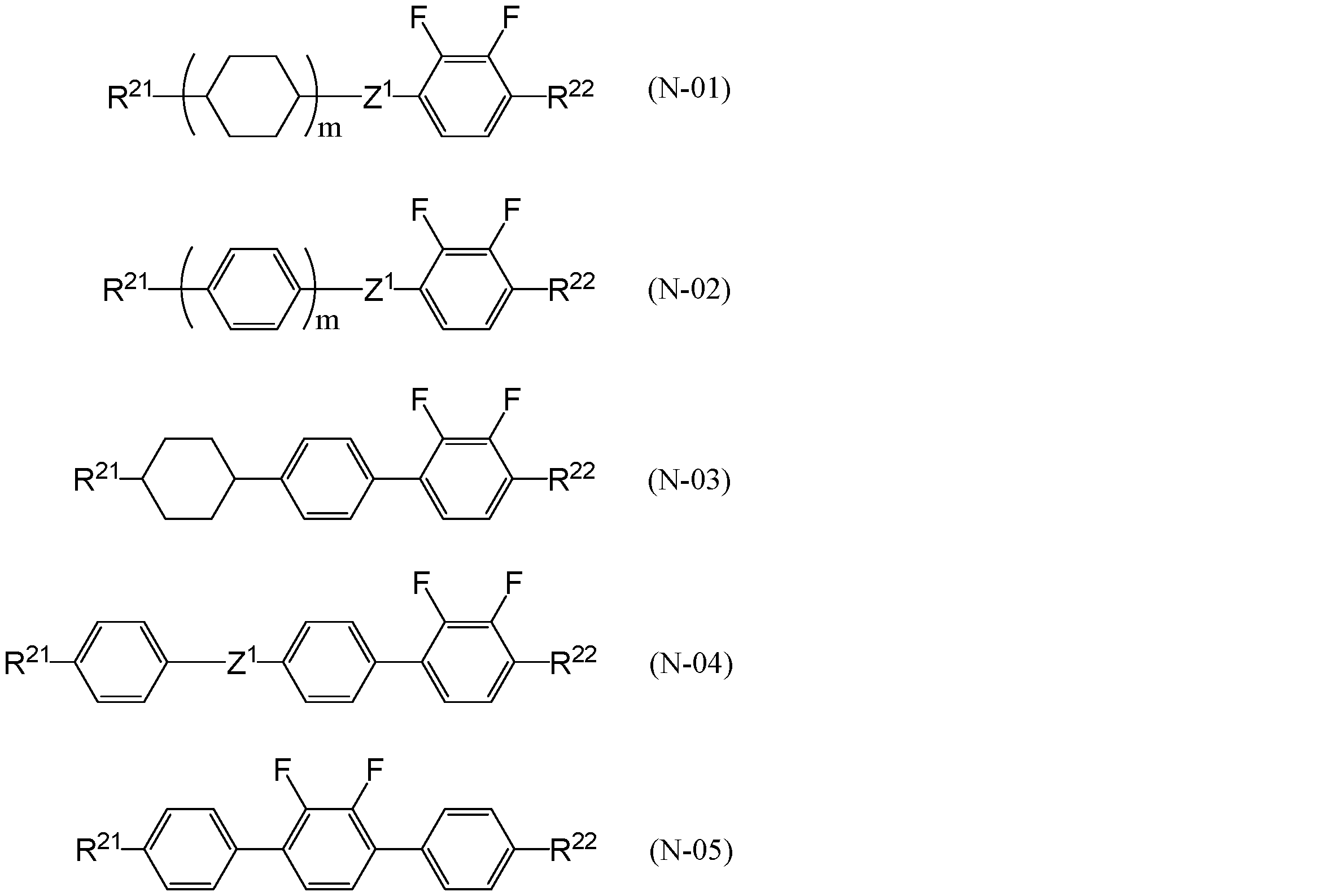
(式中、R21及びR22は、それぞれ独立して、炭素原子数1~8のアルキル基、炭素原子数1~8のアルコキシ基、炭素原子数2~8のアルケニル基、炭素原子数2~8のアルケニルオキシ基を表し、Z1は、それぞれ独立して、単結合、-CH2CH2-、-OCH2-又は-CH2O-を表し、mは、それぞれ独立して、1又は2を表す。)
一般式(N-01)で表される化合物としては、例えば一般式(N-01-1)、一般式(N-01-2)、一般式(N-01-3)及び一般式(N-01-4)で表される化合物群から選ばれる化合物が挙げられる。
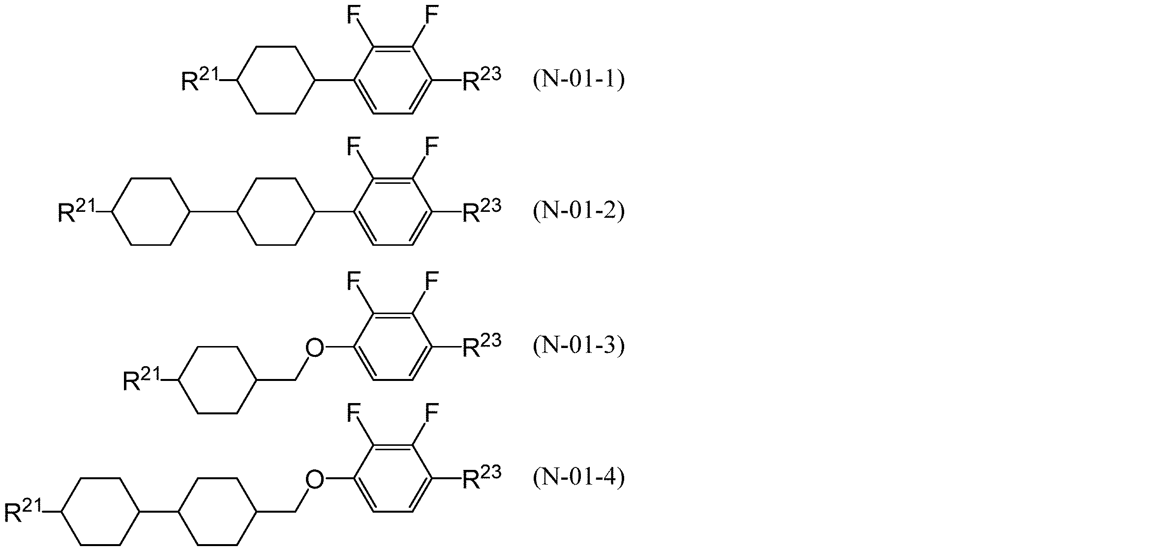
(式中、R21は、それぞれ独立して、炭素原子数1~5のアルキル基を表し、R23は、それぞれ独立して、炭素原子数1~4のアルコキシ基を表す。)
一般式(N-02)で表される化合物としては、例えば一般式(N-02-1)、一般式(N-02-2)、及び一般式(N-02-3)で表される化合物群から選ばれる化合物が挙げられる。
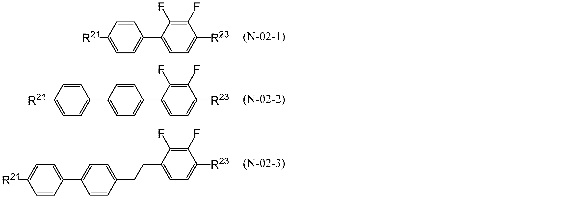
(式中、R21は、それぞれ独立して、炭素原子数1~5のアルキル基を表し、R23は、それぞれ独立して、炭素原子数1~4のアルコキシ基を表す。)
一般式(N-03)で表される化合物としては、例えば一般式(N-03-1)で表される化合物が挙げられる。

(式中、R21は、炭素原子数1~5のアルキル基を表し、R23は、炭素原子数1~4のアルコキシ基を表す。)
一般式(N-04)で表される化合物としては、例えば一般式(N-04-1)で表される化合物が挙げられる。

(式中、R21は、炭素原子数1~5のアルキル基を表し、R23は、炭素原子数1~4のアルコキシ基を表す。)
一般式(N-05)で表される化合物としては、例えば一般式(N-05-1)から一般式(N-05-3)で表される化合物が挙げられる。
液晶組成物は、誘電的に中性の化合物を1種類又は2種類以上、更に含有することができる。誘電的に中性の化合物とは、Δεが、-2より大きくかつ2より小さい値を示す化合物をいう。誘電的に中性の化合物としては、特に限定されないが、例えば一般式(NU-01)から一般式(NU-08)で表される化合物群から選ばれる化合物が挙げられる。
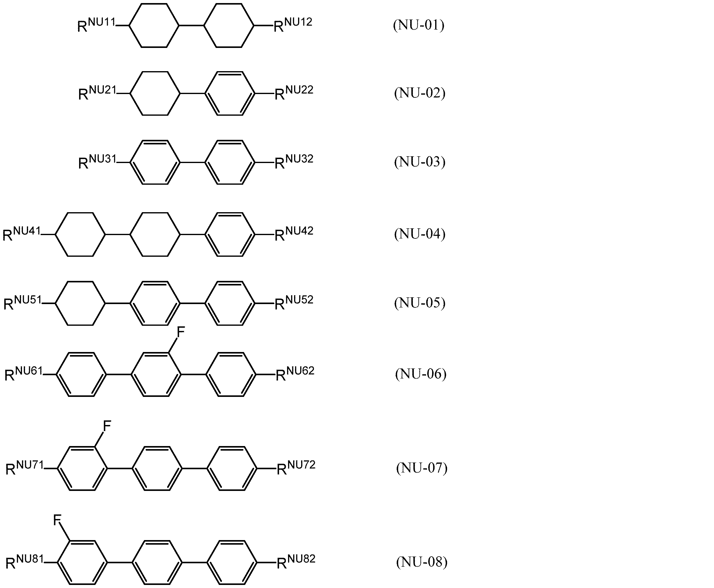
(式中、RNU11、RNU12、RNU21、RNU22、RNU31、RNU32、RNU41、RNU42、RNU51、RNU52、RNU61、RNU62、RNU71、RNU72、RNU81及びRNU82は、それぞれ独立して、炭素原子数1~8のアルキル基、炭素原子数1~8のアルコキシ基、炭素原子数2~8のアルケニル基又は炭素原子数2~8のアルケニルオキシ基を表す。)
液晶組成物は、上述の化合物の他に、重合性化合物を1種類又は2種類以上含有することができる。重合性化合物を含む液晶組成物は、重合性化合物の重合により良好な配向状態が得られるため、PSA型、PSVA型、NPS型の液晶表示素子や、配向膜を有さないPI-less型液晶表示素子に好適である。
重合性化合物としては、例えば下記一般式(RM)又は一般式(RM-13)で表される化合物からなる群から選択される化合物が挙げられる。これらは単独で用いても、2種又は3種以上を混合して用いてもよい。

(式中、R101、R102、R103、R104、R105、R106、R107及びR108は、それぞれ独立して、P13-S13-、フッ素原子に置換されてもよい炭素原子数1~18のアルキル基、フッ素原子に置換されてもよい炭素原子数1~18のアルコキシ基、フッ素原子又は水素原子のいずれかを表し、P11、P12及びP13は、それぞれ独立して、式(Re-1)から式(Re-9)

(式中、R11、R12、R13、R14及びR15は、それぞれ独立して、炭素原子数1~5のアルキル基、フッ素原子又は水素原子のいずれかを表し、mr5、mr7、nr5及びnr7は、それぞれ独立して、0、1、又は2を表すが、mr5、mr7、nr5及び/又はnr7が0を表す場合には単結合を表す。)
で表される重合性基を表し、S11、S12及びS13は、それぞれ独立して、単結合又は炭素原子数1~15のアルキレン基を表し、該アルキレン基中の1個の-CH2-又は隣接していない2個以上の-CH2-は、-O-、-OCO-又は-COO-で置換されてもよく、P13及びS13が複数存在する場合は、それぞれ、同一であっても異なっていてもよい。)

(式中、P3及びP4は、それぞれ独立して、式(PG-1)から式(PG-5)
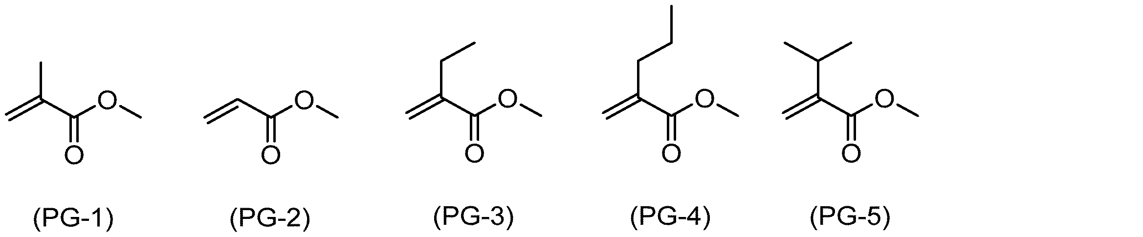
で表される重合性基を表し、S3は、単結合又は炭素原子数1~5のアルキレン基を表し、Y1からY12はそれぞれ独立してフッ素又は水素原子を表すが、少なくとも一つはフッ素原子を表す。)
で表される重合性基を表し、S11、S12及びS13は、それぞれ独立して、単結合又は炭素原子数1~15のアルキレン基を表し、該アルキレン基中の1個の-CH2-又は隣接していない2個以上の-CH2-は、-O-、-OCO-又は-COO-で置換されてもよく、P13及びS13が複数存在する場合は、それぞれ、同一であっても異なっていてもよい。)
重合性化合物は、1種又は2種以上を用いることができるが、液晶組成物中の、単独の含有量又は2以上の合計の含有量は、0.1質量%以上0.6質量%以下の範囲で調整することが好ましい。さらに、液晶組成物中の、一般式(RM)又は一般式(RM-13)で表される重合性化合物の含有量は、0.1質量%以上0.6質量%以下の範囲で調整することが好ましい。
液晶組成物は、配向助剤を1種類又は2種類以上含有してもよい。配向助剤とは、液晶分子を自発的に配向させる機能を有する化合物である。配向助剤を含む液晶組成物は、配向膜がなくても液晶分子が配向可能となるため、配向膜を有さないPI-less型液晶表示素子に好適である。
ここで配向助剤が液晶分子を自発的に配向させる機能を有するとは、配向助剤(自発配向性化合物)が、液晶組成物により構成される液晶層と直接当接する部材(電極(例えば、ITO)、基板(例えば、ガラス基板、アクリル基板、透明基板、フレキシブル基板等)、樹脂層(例えば、カラーフィルタ基板、配向膜、オーバーコート層等)、絶縁膜(例えば、無機材料膜、SiNx等))に対して相互作用し、液晶層に含まれる液晶分子のホメオトロピック配向を誘起する機能を有することをいう。
配向助剤は、重合するための重合性基と、液晶分子と類似するメソゲン基と、液晶層と直接当接する部材と相互作用可能な吸着基(極性基)と、液晶分子の配向を誘起する配向誘導基と、を有することが好ましい。
吸着基及び配向誘導基はメソゲン基に対して結合していることが好ましい。また、重合性基はメソゲン基、吸着基及び配向誘導基に直接又は必要に応じスペーサー基を介して置換していることが好ましい。
配向助剤中の配向誘導基は、液晶分子の配向を誘導する機能を有する。配向誘導基としては、例えば下記一般式(AK)で表される基が挙げられる。

(式(AK)中、RAK1は、直鎖状若しくは分岐状の炭素原子数1~20のアルキル基を表す。ただし、アルキル基中の1個又は2個以上の-CH2-は、酸素原子が直接結合することなく、それぞれ独立して、-CH=CH-、-C≡C-、-O-、-CO-、-COO-又は-OCO-で置換されてもよく、アルキル基中の1個又は2個以上の水素原子は、それぞれ独立して、ハロゲノ基で置換されてもよい。式中の*は結合手を表す。)。
配向助剤中の重合性基は、PAP1-SpAP1-で表されることが好ましい。PAP1は、下記一般式(AP-1)から一般式(AP-9)で表される群より選ばれる基であることが好ましい。

(式中、RAP1及びRAP2は、それぞれ独立して、水素原子、炭素原子数1~5のアルキル基又は炭素原子数1~10のハロゲン化アルキル基を表す。ただし、アルキル基中の1個又は2個以上の-CH2-は、-O-又は-CO-で置換されてもよく、アルキル基中の1個又は2個以上の水素原子は、それぞれ独立して、ハロゲン原子又は水酸基で置換されてもよい。WAP1は、単結合、-O-、-COO-又は-CH2-を表す。tAP1は、0、1又は2を表す。式中の*は結合手を表す。)
また、PAP1-SpAP1-で表される重合性基中、SpAP1は、単結合又は直鎖状若しくは分岐状の炭素原子数1~20のアルキレン基を表すことが好ましく、単結合又は直鎖状の炭素原子数1~20のアルキレン基を表すことがより好ましく、単結合又は直鎖状の炭素原子数2~10のアルキレン基を表すことがさらに好ましい。また、SpAP1において、アルキレン基中の1個又は隣接しない2個以上の-CH2-は、それぞれ独立して、-CH=CH-、-C≡C-、-O-、-CO-、-COO-又は-OCO-で置換されてもよい。
配向助剤において、重合性基(PAP1-SpAP1-)の数は、1以上5以下であることが好ましく、1以上4以下であることがより好ましく、2以上4以下であることがさらに好ましく、2又は3であることが特に好ましく、2であることが最も好ましい。
PAP1-SpAP1-中の水素原子は、重合性基、吸着基及び/又は配向誘導基で置換されてもよい。重合性基(PAP1-SpAP1-)は、重合性基、メソゲン基、吸着基及び/又は配向誘導基に対して結合してもよい。また、重合性基(PAP1-SpAP1-)は、メソゲン基、吸着基又は配向誘導基に対して結合することが好ましく、メソゲン基又は吸着基に対して結合することがより好ましい。なお、分子内にPAP1及び/又はSpAP1-が複数存在する場合に、それぞれ互いに同一であっても異なってもよい。
配向助剤中のメソゲン基は、剛直な部分を備えた基、例えば環式基を1つ以上備えた基をいい、環式基を2個~4個を備えた基が好ましく、環式基を3個~4個を備えた基がより好ましい。なお、必要に応じて、環式基は、連結基で連結されてもよい。メソゲン基は、液晶層に使用される液晶分子(液晶化合物)と類似の骨格を有することが好ましい。なお、「環式基」とは、構成する原子が環状に結合した原子団のことをいい、炭素環、複素環、飽和又は不飽和環式構造、単環、2環式構造、多環式構造、芳香族、非芳香族などを含む。
また、環式基は、少なくとも1つのヘテロ原子を含んでもよく、さらに、少なくとも1つの置換基(ハロゲノ基、重合性基、有機基(アルキル、アルコキシ、アリール等)で置換されてもよい。環式基が単環である場合には、メソゲン基は、2個以上の単環を含んでいることが好ましい。
上記メソゲン基は、例えば、一般式(AL)で表されることが好ましい。

(式(AL)中、ZAL1は、単結合、-CH=CH-、-CF=CF-、-C≡C-、-COO-、-OCO-、-OCOO-、-CF2O-、-OCF2-、-CH=CHCOO-、-OCOCH=CH-、-CH2-CH2COO-、-OCOCH2-CH2-、-CH=C(CH3)COO-、-OCOC(CH3)=CH-、-CH2-CH(CH3)COO-、-OCOCH(CH3)-CH2-、-OCH2CH2O-又は炭素原子数1~20のアルキレン基を表す。ただし、アルキレン基中の1個又は隣接しない2個以上の-CH2-は、-O-、-COO-又は-OCO-で置換されてもよい。AAL1及びAAL2は、それぞれ独立して、2価の環式基を表す。ZAL1、AAL1及びAAL2中の1個又は2個以上の水素原子は、それぞれ独立して、ハロゲノ基、吸着基、PAP1-SpAP1-又は1価の有機基で置換されてもよく、分子内にZAL1及びAAL1が複数存在する場合に、それぞれ互いに同一であっても異なってもよい。mAL1は、1~5の整数を表す。式中の*は結合手を表す。)
配向助剤中の吸着基は、基板、膜、電極など液晶組成物と当接する層である吸着媒と吸着する役割を備えた基である。吸着は、吸着媒と吸着質との間で化学結合(共有結合、イオン結合又は金属結合)が形成されることにより吸着する化学吸着であってもよく、化学吸着以外の物理吸着であってもよいが、物理吸着であることが好ましい。吸着基としては、例えば下記一般式(AT)で表される基が挙げられる。

(式(AT)中、SpAT1は、単結合、炭素原子数1~25の直鎖状若しくは分岐状のアルキレン基を表す。ただし、アルキレン基中の水素原子は、-OH、-CN、-WAT1-ZAT1又はPAP1-SpAP1-で置換されてもよく、アルキレン基中の-CH2-は、酸素原子が直接結合しないように環式基、-O-、-COO-、-C(=O)-、-OCO-、-CH=CH-又は-OCO-COO-で置換されてもよい。ZAT1は、極性要素を含む1価の基を表す。ただし、ZAT1中の水素原子は、-OH、-CN、-SpAT1-WAT1-ZAT1又はPAP1-SpAP1-で置換されてもよい。WAT1は、単結合又は下記一般式(WAT1)又は(WAT2)

(式(WAT1)及び(WAT2)中、SpWAT1及びSpWAT2は、それぞれ独立して、単結合、炭素原子数1~25の直鎖状若しくは分岐状のアルキレン基を表し、アルキレン基中の水素原子は、-OH、-CN、-SpAT1-WAT1-ZAT1又はPAP1-SpAP1-で置換されてもよく、アルキレン基中の-CH2-は、酸素原子が直接結合しないように環式基、-O-、-COO-、-C(=O)-、-OCO-又は-CH=CH-で置換されてもよい。式中の*は結合手を表す。)を表す。なお、式(AT)中の*は結合手を表す。)
液晶組成物中に含まれる配向助剤の量は、0.01質量%以上50質量%以下程度であることが好ましい。液晶組成物中の配向助剤の含有量のより好ましい下限値は、液晶分子を更に好適に配向させる観点から、0.05質量%であり、0.1質量%である。また、より好ましい上限値は、応答特性を改善する観点から、5質量%であり、3質量%であり、2質量%であり、1質量%である。
液晶組成物は、酸化防止剤を1種類又は2種類以上含むことが好ましく、中でもヒンダードフェノール系の酸化防止剤を含むことが好ましい。また、液晶組成物は、上述の化合物以外に、通常のネマチック液晶、スメクチック液晶、コレステリック液晶、紫外線吸収剤、光安定剤、赤外線吸収剤等を含有してもよい。
液晶組成物は、ネマチック相-等方性液体相転移温度(TNI)の下限が、60℃であることが好ましく、70℃が好ましく、80℃が好ましく、90℃が好ましく、一方、上限が、120℃であることが好ましく、110℃が好ましく、100℃が好ましく、90℃が好ましく、85℃が好ましく、80℃が好ましい。なお、60℃以上をTNIが高いと表現している。より詳しくは、液晶テレビ用途の場合、TNIは70℃以上80℃以下が好ましく、モバイル用途の場合、TNIは80℃以上90℃以下が好ましく、PID(Public Information Display)等の屋外表示用途の場合、TNIは90℃以上110℃以下が好ましい。
液晶組成物は、20℃における屈折率異方性(Δn)が0.08以上0.14以下であることが好ましく、0.09以上0.13以下がさらに好ましく、0.09以上0.12以下がより好ましく、0.098以上0.118以下が特に好ましい。更に詳述すると、薄いセルギャップに対応する場合は、20℃における屈折率異方性(Δn)が0.10以上0.13であることが好ましく、一方、厚いセルギャップに対応する場合は、20℃における屈折率異方性(Δn)が0.08以上0.10以下であることが好ましい。
液晶組成物は、20℃における回転粘性(γ1)が50Pa・s以上160mPa・s以下であることが好ましく、55Pa・s以上160mPa・s以下であることが好ましく、60Pa・s以上160mPa・s以下であることが好ましく、80Pa・s以上150mPa・s以下であることが好ましく、90Pa・s以上140mPa・s以下であることが好ましく、90Pa・s以上130mPa・s以下であることが好ましく、90Pa・s以上115mPa・s以下であることが好ましい。
液晶組成物は、20℃における誘電率異方性(Δε)が-1.7以上-4.0以下であることが好ましく、-2.5以上-3.8以下がさらに好ましく、-2.6以上-3.7以下がより好ましく、-2.7以上-3.6以下が特に好ましい。
画素電極5及び共通電極6は、それぞれ、例えば透明電極である。透明電極は、酸化物半導体(ZnO、InGaZnO、SiGe、GaAs、IZO(Indium Zinc Oxide)、ITO(Indium Tin Oxide)、SnO、TiO、AZTO(AlZnSnO)等)をスパッタリング等することにより形成される。透明電極は、アモルファスのITO膜を焼成することにより、多結晶のITO膜として形成されてもよい。
カラーフィルタ基板7は、ブラックマトリックス7aと、ブラックマトリックス7aに二次元に配列された複数の開口部(画素部)7bとを備え、複数の開口部7bのそれぞれには、光源(図示せず)からの光のうち特定波長域の光を選択透過する赤色、緑色又は青色のカラーフィルタ(図示せず)が設けられている。複数の開口部(画素部)7bは、設けられているカラーフィルタの色に応じて、赤色画素部(R)、緑色画素部(G)又は青色画素部(B)として機能する。
カラーフィルタ基板7の平面形状は、例えば長方形状であってよい。本実施形態では、カラーフィルタ基板7の平面形状は、図1に示すx方向を長手方向とする長方形状となっている。カラーフィルタ基板7においては、例えば、カラーフィルタ基板7の長手方向(x方向)に沿って、赤色画素部(R)、緑色画素部(G)及び青色画素部(B)がこの順で繰り返し配列されており、かつ、カラーフィルタ基板7の短手方向(y方向)に沿って、同色の画素部が配列されている。この場合、各画素部(開口部)7bの平面形状は、例えば、カラーフィルタ基板7の短手方向(y方向)に長い長方形状であってよい。
他の一実施形態では、カラーフィルタ基板7においては、例えば、カラーフィルタ基板7の短手方向(y方向)に沿って、赤色画素部(R)、緑色画素部(G)及び青色画素部(B)がこの順で繰り返し配列されており、かつ、カラーフィルタ基板7の長手方向(x方向)に沿って、同色の画素部が配列されている。この場合、各画素部(開口部)7bの平面形状は、例えば、カラーフィルタ基板7の長手方向(x方向)に長い長方形状であってよい。
言い換えれば、一実施形態では、後述するゲートバスライン11の延在方向に沿って、赤色画素部(R)、緑色画素部(G)及び青色画素部(B)がこの順で繰り返し配列されていてもよい。この場合、各画素部(開口部)7bの平面形状が、後述するデータバスライン12の延在方向に長い長方形状であってよい。また、他の一実施形態では、データバスライン12の延在方向に沿って赤色画素部(R)、緑色画素部(G)及び青色画素部(B)がこの順で繰り返し配列されていてもよい。この場合、各画素部(開口部)7bの平面形状が、ゲートバスライン11の方向に長い長方形状であってよい。
第1の偏光板8及び第2の偏光板9は、公知の偏光板であってよく、例えば、二色性有機色素偏光板、塗布型偏光板、ワイヤーグリッド型偏光板、コレステリック液晶型偏光板等であってよい。
液晶表示素子1は、液晶層4と第1の基板2との間、及び液晶層4と第2の基板3との間に、それぞれ配向膜(図示せず)が配置されていてもよい。配向膜は、液晶分子4aを配向させる機能を有するものであり、通常、液晶層4と直接接する部材である。配向膜としては、ポリイミド膜、ナイロン膜、ポリビニルアルコール膜などの有機高分子膜が好ましく用いられる。液晶層4を構成する液晶組成物が配向助剤を含む場合、液晶層4と第1の基板2との間、及び液晶層4と第2の基板3との間の少なくとも一方に、配向膜が配置されていなくてもよく、両方に配向膜が配置されていなくてもよい。配向助剤の存在により、配向膜が配置されていなくても、液晶分子4aが自発的に配向することが可能となる。この場合、液晶表示素子1は、第1の基板2及び第2の基板3の間に、重合性化合物及び/又は配向助剤の重合物を有することができる。
図2は、画素電極5の一実施形態を示す平面図(画素電極5を液晶層4側から見た平面図。以下同様。)である。図2に示すように、一実施形態に係る画素電極5Aは、走査信号を供給する一対のゲートバスライン11,11と、表示信号を供給する一対のデータバスライン12,12とで囲まれて画定される領域(単位画素)内に設けられている。
一対のゲートバスライン11,11同士は、略平行に一方向(x方向とする)に延在している。一対のデータバスライン12,12同士は、略平行に一方向(y方向とする)に延在している。ゲートバスライン11とデータバスライン12とは、互いに略直交している。
このような一対のゲートバスライン11,11及び一対のデータバスライン12,12によって形成される単位画素の平面形状は、例えば、正方形状、長方形状等の矩形状であってよく、好ましくは長方形状である。当該長方形状は、データバスライン12の延在方向(後述する第1~4の領域R1~R4の配列方向)に長い長方形状であってよく、ゲートバスライン11の延在方向に長い長方形状であってもよく、好ましくはデータバスライン12の延在方向(第1~4の領域R1~R4の配列方向)に長い長方形状である。単位画素の平面形状が長方形状である場合、正方形状である場合よりも、本実施形態における画素電極5を用いたときの単位画素あたりの光の透過領域の割合をより大きくすることができる(詳細は後述)。
同様の観点から、単位画素の長手方向の長さは、短手方向の長さに対して、好ましくは1.5倍以上、より好ましくは2倍以上、更に好ましくは2.5倍以上である。より高透過率及び高開口率を得ることができ、また高精細化の観点から、単位画素の長手方向の長さは、短手方向の長さに対して、好ましくは3倍以下である。単位画素の長手方向の長さは、短手方向の長さに対して、好ましくは1.5~3倍、より好ましくは2~3倍、更に好ましくは2.5~3倍であってもよい。
単位画素の平面形状が長方形状である場合、単位画素の長手方向の長さは、例えば、50μm以上又は100μm以上であってよく、1000μm以下又は600μm以下であってよい。単位画素の短手方向の長さは、透過率の向上といった効果がより顕著に得られ、かつ液晶分子4aの配向の均一化が図られる観点から、好ましくは15μm以上、より好ましくは30μm以上、更に好ましくは50μm以上である。単位画素の短手方向の長さは、液晶分子4aの配向具合(応答性)にばらつきが生じるのを抑制できる観点から、好ましくは1000μm以下、より好ましくは600μm以下、更に好ましくは300μm以下である。
ゲートバスライン11及びデータバスライン12は、それぞれ金属で形成されており、例えば、Al、Cu、Au、Ag、Cr、Ta、Ti、Mo、W、Ni又はその合金で形成されている。
一方のゲートバスライン11と一方のデータバスライン12とが互いに交差する交差部(単位画素の角部)近傍には、当該ゲートバスライン11及びデータバスライン12に接続されたソース電極13及びドレイン電極14を含む薄膜トランジスタ15が設けられている。
画素電極5Aは、液晶分子4aを互いに異なる方位へ傾斜させる第1の領域R1、第2の領域R2、第3の領域R3及び第4の領域R4を含んでいる。第1の領域R1、第2の領域R2、第3の領域R3及び第4の領域R4は、この順に一方向(y方向)に一列に配列されている。なお、図2で示す実施形態においては、第1の領域R1、第2の領域R2、第3の領域R3及び第4の領域R4は、データバスライン12の延在方向(y方向)に沿ってこの順に配置されているが、第1の領域R1、第2の領域R2、第3の領域R3及び第4の領域R4は、他の一実施形態では、ゲートバスライン11の延在方向(x方向)に沿ってこの順に配置されていてもよい。後者の場合、単位画素の平面形状は、好ましくは、ゲートバスライン11の延在方向(x方向)に長い長方形である。
画素電極5Aは、第1の領域R1及び第2の領域R2に沿って一方向(y方向)に延在する第1の幹部51aと、第3の領域R3及び第4の領域R4に沿って一方向(y方向)に延在する第2の幹部51bとを有している。第1の幹部51aは、第1の領域R1及び第2の領域R2の一方のデータバスライン12側に設けられている。第2の幹部51bは、第3の領域R3及び第4の領域R4の他方のデータバスライン12側に設けられている。つまり、第1の幹部51aと第2の幹部51bとは、同一直線上には存在していない。
画素電極5Aは、第1の幹部51aに接続され、第1の領域R1と第2の領域R2とを互いに隔てるように設けられた第3の幹部51cを更に有している。言い換えれば、第3の幹部51cは、第1の幹部51aと略垂直な方向(x方向)に延在するように、第1の領域R1と第2の領域R2との間に設けられている。
画素電極5Aは、第2の幹部51bに接続され、第3の領域R3と第4の領域R4とを互いに隔てるように設けられた第4の幹部51dを更に有している。言い換えれば、第4の幹部51dは、第2の幹部51bと略垂直な方向(x方向)に延在するように、第3の領域R3と第4の領域R4との間に設けられている。
画素電極5Aは、第1の領域R1において、第1の幹部51a及び第3の幹部51cのそれぞれから、所定の方向D1に向けて互いに略平行に延在する複数の第1の枝部52aを更に有している。第1の枝部52aは、第1の幹部51aを起点に第3の幹部51cが延在する方向を0°とし、反時計回りを正の角度としたときに(以下、角度を示すときの基準は同じ)、略45°の方向に延在している。これにより、第1の領域R1上に存在する液晶分子4aは、第1の枝部52a上で第1の枝部52aの延在方向D1と逆方向d1(略225°の方向)に沿った方位に傾斜(配向)する。
画素電極5Aは、第2の領域R2において、第1の幹部51a及び第3の幹部51cのそれぞれから、所定の方向D2に向けて互いに略平行に延在する複数の第2の枝部52bを更に有している。第2の枝部52bは、略315°の方向に延在している。言い換えれば、第1の枝部52aの延在方向D1と第2の枝部52bの延在方向D2とのなす角度は、略90°となっている。これにより、第2の領域R2上に存在する液晶分子4aは、第2の枝部52b上で第2の枝部52bの延在方向D2と逆方向d2(略135°の方向)に沿った方位に傾斜(配向)する。
画素電極5Aは、第3の領域R3において、第2の幹部51b及び第4の幹部51dのそれぞれから、所定の方向D3に向けて互いに略平行に延在する複数の第3の枝部52cを更に有している。第3の枝部52cは、略135°の方向に延在している。言い換えれば、第2の枝部52bの延在方向D2と第3の枝部52cの延在方向D3とのなす角度は、略180°となっている。
これにより、第3の領域R3上に存在する液晶分子4aは、第3の枝部52c上で第3の枝部52cの延在方向D3と逆方向d3(略315°の方向)に沿った方位に傾斜(配向)する。言い換えれば、第2の領域R2上に存在する液晶分子4aの傾斜方向と第3の領域R3上に存在する液晶分子4aの傾斜方向とのなす角度は、略180°である。すなわち、第2の領域R2上に存在する液晶分子4aの傾斜方向と第3の領域R3上に存在する液晶分子4aの傾斜方向とは、相反している。そのため、第2の領域R2上に存在する液晶分子4aの配向と第3の領域R3上に存在する液晶分子4aの配向との間で相互作用が生じにくく、第2の領域R2及び第3の領域R3の境界付近の液晶分子4aの配向安定性を高めることができる。
画素電極5Aは、第4の領域R4において、第2の幹部51b及び第4の幹部51dのそれぞれから、所定の方向D4に向けて互いに略平行に延在する複数の第4の枝部52dを更に有している。第4の枝部52dは、略225°の方向に延在している。言い換えれば、第3の枝部52cの延在方向D3と第4の枝部52dの延在方向D4とのなす角度は、略90°となっている。これにより、第4の領域R4上に存在する液晶分子4aは、第4の枝部52d上で第4の枝部52dの延在方向D4と逆方向d4(略45°の方向)に沿った方位に傾斜(配向)する。
第1の幹部51a、第2の幹部51b、第3の幹部51c及び第4の幹部51dの短手方向(延在方向と垂直な方向)の長さは、それぞれ、例えば、2μm以上又は5μm以上であってよく、10μm以下又は7μm以下であってよい。第1の枝部52a、第2の枝部52b、第3の枝部52c及び第4の枝部52dの短手方向(延在方向と垂直な方向)の長さは、それぞれ、例えば、1μm以上又は2μm以上であってよく、5μm以下又は4μm以下であってよい。
各領域R1~R4において、複数の枝部52a~52d同士は、所定の間隔(スペース)を空けて配置されている。すなわち、隣り合う枝部52a~52d間には、スペースが存在する。複数の枝部52a~52dにおけるラインアンドスペース(L/S)は、光の透過領域をより広くでき高透過率が得られる観点から、好ましくは1μm/1μm~5μm/5μm、より好ましくは2μm/2μm~4μm/4μm、更に好ましくは2μm/2μm~3μm/3μmである。ラインアンドスペースを上記の関係とすることで、光の透過領域をより確保でき高透過率が得られる。なお、L及びSは、それぞれ枝部の線幅(上記の枝部の短手方向の長さと同義)及び隣り合う枝部間の間隔を意味する。
画素電極5Aでは、例えば、第1の幹部51aの第1の領域R1側の先端が、薄膜トランジスタ15のドレイン電極14に接続されている。画素電極5Aでは、例えば、第1の幹部51aの第2の領域R2側の先端が、第3の枝部52cの少なくとも一つと電気的に接続され、また、第2の幹部51bの第3の領域R3側の先端が、第2の枝部52bの少なくとも一つと電気的に接続されていることによって、第2の領域R2と第3の領域R3との間の導通がとられている。これにより、薄膜トランジスタ15(ドレイン電極14)から画素電極5Aに給電することが可能となっている。
第2の領域R2と第3の領域R3との間には、幹部51a,51b及び枝部52a~52dのいずれもが配置されていない空間(領域)Sが設けられている。第2の領域R2と第3の領域R3とが空間Sにより互いに隔てられていることで、第2の領域R2及び第3の領域R3の境界付近に存在する第2の領域R2上の液晶分子4aと第3の領域R3上の液晶分子4aとが、互いの液晶配向に影響を及ぼすことを防ぐことができる。その結果、第2の領域R2及び第3の領域R3の境界付近の液晶分子4aの配向安定性を維持することができる。4つの領域R1~R4の配列方向(y方向)における空間Sの長さ(幅)は、狭いほど好ましく、より好ましくは、上述した各領域R1~R4において隣り合う枝部間の間隔より大きい。当該空間Sの長さ(幅)は、例えば、5μm以上であってよく、10μm以下であってよく、好ましくは7~9μmであり、8μmであってもよい。
この液晶表示素子1における画素電極5Aでは、液晶分子4aを互いに異なる方位へ傾斜させる4つの領域R1~R4が、一方向(y方向)に配列されている。そして、この画素電極5Aでは、所定の方向D1~D4に向けて延在する各枝部52a~52dが当該領域R1~R4にそれぞれ設けられていることにより、第1の幹部51a及び第2の幹部51bが、それぞれ、4つの領域R1~R4のうち2つの領域R1,R2及びR3,R4に沿って当該領域R1~R4の配列方向に延在してさえいれば、PSA型液晶表示素子に適用した場合に、4つの異なる液晶ドメインを形成することができる。つまり、この画素電極5Aでは、第1の幹部51a及び第2の幹部51bが、従来のように画素の中央に十字形状に設けられている必要がなく、例えば画素の端部に設けられてもよい。このように、この画素電極5Aは、PSA型液晶表示素子に適用可能な画素電極であって、第1の幹部51a及び第2の幹部51bを自在に配置することを可能にするものである。
このように、この画素電極5Aによれば、第1の幹部51a及び第2の幹部51bを自在に配置することができるため、単位画素における光の透過領域が広くなるように、第1の幹部51a及び第2の幹部51bを配置することが可能となる。
例えば、図2に示すように、第1の幹部51a及び第2の幹部51bは、一実施形態において、単位画素の端部(周縁部)に設けることができる。この場合、図3(a)に示すように、第1の基板2、液晶層4、第2の基板3等の各層の積層方向(以下、単に「積層方向」ともいう)から見たときに、第1の幹部51a及び第2の幹部51bの全部が、画素電極5Aに対応する画素の開口部(画素電極5Aの直上に配置されている開口部)7bと重ならない位置に設けられることになる。
一方、図3(b)に示すように、従来のいわゆるフィッシュボーン構造を有する画素電極500では、データバスライン12と略平行に延在する第1の幹部501aと、ゲートバスライン11と略平行に延在する第2の幹部501bとが、単位画素の略中央で互いに交差するような十字形状に配置されている。そして、第1の幹部501a及び第2の幹部501bによって画定される4つの領域ごとに、互いに延在方向が異なる枝部502a,502b,502c,502dが設けられていることにより、当該4つの領域に対応して、液晶分子4aのディレクタの方位が互いに異なる4つの液晶ドメインが形成されている。この場合、第1の幹部501aが、画素電極500に対応する画素の開口部(画素電極500の直上に配置されている開口部)7bと重なる位置に設けられることになる。
したがって、本実施形態に係る画素電極5Aでは、暗線の発生及び透過率の低下の原因となる第1の幹部51a及び第2の幹部51bが開口部7bと重ならないため、第1の幹部501aが開口部7bと重なるような構成を有する従来の画素電極500と比べて、単位画素における光の透過領域が更に広くなり、暗線の発生の抑制及び透過率の向上が可能となる。なお、積層方向から見たときに、第1の幹部51a及び第2の幹部51bの少なくとも一部が画素電極5Aに対応する画素の開口部(画素電極5Aの直上に配置されている開口部)7bと重ならない位置に設けられていれば、同様の効果を得ることができる。
また、このような効果は、上述したとおり、単位画素の平面形状が第1~4の領域R1~R4の配列方向に長い長方形状である場合に特に好適に得られる。すなわち、単位画素の平面形状が当該第1~4の領域R1~R4の配列方向に長い長方形状であると、当該配列方向に延在する第1の幹部51a及び第2の幹部51bの長さも長くなり、単位画素に占める第1の幹部51a及び第2の幹部51bの面積割合も大きくなるため、第1の幹部51a及び第2の幹部51bが開口部7bと重ならないように配置されることによる暗線の発生の抑制及び透過率の向上の効果が顕著となる。
また、例えば、他の一実施形態において、補助容量を形成させるためのCs電極(図示せず)が第1の基板2上に設けられている場合に、第1の幹部51a及び第2の幹部51bは、積層方向から見たときに、それらの少なくとも一部がCs電極と重なる位置に設けることもできる。この場合、暗線の発生及び透過率の低下の原因となる第1の幹部51a及び第2の幹部51bと、同じく暗線の発生及び透過率の低下の原因となり得るCs電極とが互いに重なって配置されるため、単位画素において光を透過させない領域が狭くなり(光を透過させる領域が広くなり)、その結果、暗線の発生の抑制及び透過率の向上が可能となる。
このような効果が好適に得られる観点から、積層方向から見たときに、第1の幹部51a及び第2の幹部51bの全部がCs電極と重なる位置に設けられていることが好ましく、第1の幹部51a及び第2の幹部51bの全部とCs電極とが、画素電極5Aに対応する画素の開口部(画素電極5Aの直上に配置されている開口部)7bと重ならない位置で互いに重なるように設けられていることがより好ましい。また、同様の観点から、積層方向から見たときに、第3の幹部51c及び第4の幹部51dも、好ましくは、Cs電極と重なる位置に設けられている。
以上説明した画素電極5では、上述したとおり、第1の幹部51a及び第2の幹部51bを自在に配置することができるため、画素電極5は、上記実施形態以外にも種々の実施形態をとり得る。
図4は、画素電極5の他の一実施形態を示す平面図である。上記実施形態では、第1の幹部51aは、第1の領域R1及び第2の領域R2に対応する位置のみに延在しており、第2の幹部51bは、第3の領域R3及び第4の領域R4に対応する位置のみに延在しているが、他の一実施形態では、図4に示すように、第1の幹部51a及び第2の幹部51bのそれぞれが、第1~4の領域R1~R4のすべてにわたって対応する位置に延在していてよい。
この場合、一対のデータバスライン12,12それぞれの全体にわたって、その近傍に第1の幹部51a及び第2の幹部51bが設けられているため、画素電極5Bとデータバスライン12との間の寄生容量が安定する。すなわち、この画素電極5Bは、例えば図2に示した画素電極5Aに比べて、第1~4の枝部52a~52dの寸法にばらつきが生じた場合であっても、第1の幹部51a及び第2の幹部51bがそのばらつきによって生じ得る寄生容量の変動を抑制できる。
図5は、画素電極5の他の一実施形態を示す平面図である。上記実施形態では、第1の幹部51a及び第2の幹部51bそれぞれの一方側のみに第1~4の枝部52a~52dが設けられているが、他の一実施形態では、図5に示すように、第1の幹部51a及び第2の幹部51bの第1~4の枝部52a~52dが設けられている側と反対側に補助枝部が更に設けられていてよい。
より具体的には、画素電極5Cは、第1の幹部51aに対して第1の枝部52aの延在方向D1と略対称の方向(略135°の方向)D5に延在する第1の補助枝部53aを更に有している。画素電極5Cは、第2の幹部51bに対して第2の枝部52bの延在方向D2と略対称の方向(略225°の方向)D6に延在する第2の補助枝部53bを更に有している。画素電極5Cは、第3の幹部51cに対して第3の枝部52cの延在方向D3と略対称の方向(略45°の方向)D7に延在する第3の補助枝部53cを更に有している。画素電極5Cは、第4の幹部51dに対して第4の枝部52dの延在方向D4と略対称の方向(略315°の方向)D8に延在する第4の補助枝部53dを更に有している。
第1~4の補助枝部53a~53dの短手方向(延在方向と垂直な方向)の長さは、例えば、1μm以上又は2μm以上であってよく、5μm以下又は4μm以下であってよい。第1~4の補助枝部53a~53dの長手方向(延在方向)の長さは、光透過率を向上させるのに有利である点から、好ましくは、第1~4の枝部52a~52dの長さより短く、3μm以上又は5μm以上であってよい。第1~4の補助枝部53a~53dの長手方向(延在方向)の長さは、第1の幹部51a及び第2の幹部51b近傍の液晶分子4aの配向を更に安定させる観点から、好ましくは、15μm以下又は10μm以下であってよい。
複数の補助枝部53a~53d同士は、所定の間隔(スペース)を空けて配置されている。すなわち、隣り合う補助枝部53a~53d間には、スペースが存在する。複数の補助枝部53a~53dにおけるラインアンドスペース(L/S)は、光の透過領域をより広くでき高透過率が得られる観点から、好ましくは1μm/1μm~5μm/5μm、より好ましくは2μm/2μm~4μm/4μmである。なお、L及びSは、それぞれ補助枝部の線幅(上記の補助枝部の短手方向の長さと同義)及び隣り合う枝部間の間隔を意味する。
この画素電極5Bでは、第1の枝部52aの延在方向D1と略対称の方向D5に延在する第1の補助枝部53aが設けられていることにより、第1の補助枝部53a上に存在する液晶分子4aは、第1の枝部52a上の液晶分子4aの傾斜(配向)方向d1と略対称の方向d5(略315°の方向)に沿った方位に傾斜(配向)する。また、第2の枝部52bの延在方向D2と略対称の方向D6に延在する第2の補助枝部53bが設けられていることにより、第2の補助枝部53b上に存在する液晶分子4aは、第2の枝部52b上の液晶分子4aの傾斜(配向)方向d2と略対称の方向d6(略225°の方向)に沿った方位に傾斜(配向)する。そのため、第1の幹部51a近傍の液晶分子4aの配向を安定化させることができる。
同様に、第3の枝部52cの延在方向D3と略対称の方向D7に延在する第3の補助枝部53cが設けられていることにより、第3の補助枝部53c上に存在する液晶分子4aは、第3の枝部52c上の液晶分子4aの傾斜(配向)方向d3と略対称の方向d7(略45°の方向)に沿った方位に傾斜(配向)する。また、第4の枝部52dの延在方向D4と略対称の方向D8に延在する第4の補助枝部53dとが設けられていることにより、第4の補助枝部53d上に存在する液晶分子4aは、第4の枝部52d上の液晶分子4aの傾斜(配向)方向d4と略対称の方向d8(略135°の方向)に沿った方位に傾斜(配向)する。そのため、第2の幹部51b近傍の液晶分子4aの配向を安定化させることができる。
図6は、画素電極5の他の一実施形態を示す平面図である。上記実施形態では、第1~4の領域R1~4の配列方向に延在する幹部として第1の幹部51a及び第2の幹部51bが設けられているが、他の一実施形態では、図6に示すように、第1~4の領域R1~R4の第1の幹部51a又は第2の幹部51bが設けられている側と反対側に、第1~4の領域R1~4の配列方向に延在する幹部が更に設けられていてよい。なお、図6は、このような実施形態の一例として、図5に示した実施形態に当該幹部が更に設けられた実施形態を示している。
より具体的には、画素電極5Dは、第1の領域R1及び第2の領域R2の第1の幹部51aが設けられている側と反対側に、第1~4の領域R1~4の配列方向(すなわち、第1の幹部51aの延在方向と略平行な方向)に延在する第5の幹部51eを更に有している。画素電極5Dは、第3の領域R3及び第4の領域R4の第2の幹部51bが設けられている側と反対側に、第1~4の領域R1~4の配列方向(すなわち、第2の幹部51bの延在方向と略平行な方向)に延在する第6の幹部51fを更に有している。
第5の幹部51eの第2の領域R2側の先端は、例えば第2の幹部51bに接続されている。第6の幹部51fの第3の領域R3側の先端は、例えば第1の幹部51aに接続されている。第5の幹部51e及び第6の幹部51fの短手方向(延在方向と垂直な方向)の長さは、それぞれ、例えば、2μm以上又は5μm以上であってよく、10μm以下又は7μm以下であってよい。
この画素電極5Dでは、第1~4の領域R1~R4の第1の幹部51a又は第2の幹部51bが設けられている側と反対側に第5の幹部51e及び第6の幹部51fが更に設けられているため、一対のデータバスライン12,12の両方の近傍に、データバスライン12,12の延在方向と略平行に延在する幹部が設けられることになる。したがって、画素電極5Cとデータバスライン12,12との間の容量の変化を抑えることができる。
図7は、画素電極5の他の一実施形態を示す平面図である。図6に示した実施形態では、第5の幹部51eは、第1の領域R1及び第2の領域R2に対応する位置のみに延在しており、第6の幹部51fは、第3の領域R3及び第4の領域R4に対応する位置のみに延在しているが、他の一実施形態では、図7に示すように、第5の幹部51e及び第6の幹部51fのそれぞれが、第1~4の領域R1~R4のすべてにわたって対応する位置に延在していてよい。
この場合、一対のデータバスライン12,12それぞれの全体にわたって、その近傍に第5の幹部51e及び第6の幹部51fが設けられているため、画素電極5Eとデータバスライン12との間の寄生容量が安定する。すなわち、この画素電極5Eは、例えば図6に示した画素電極5Dに比べて、第1~4の補助枝部53a~53dの寸法にばらつきが生じた場合であっても、第5の幹部51e及び第6の幹部51fがそのばらつきによって生じ得る寄生容量の変動を抑制できる。
以下、実施例に基づいて本発明を更に具体的に説明するが、本発明は以下の実施例に限定されるものではない。
図3に示す画素電極5A(実施例1)及び画素電極500(比較例1)のような画素電極をそれぞれ有する液晶表示素子について、透過率のシミュレーションを行った(シンテック社製LCDマスタ3Dを使用)。実施例1及び比較例1に共通する条件は、以下のとおりである。
液晶層:Δn=0.110、Δε=-3.3、K11=14.8、K33=13.6、厚み:3.2μm
共通電極:ベタ電極
単位画素:90μm×200μmの長方形状
開口部:単位画素の各辺から5μm内側に配置された80μm×190μmの長方形状
計算領域:単位画素を含む100μm×210μmの長方形状
電圧:8V
液晶層:Δn=0.110、Δε=-3.3、K11=14.8、K33=13.6、厚み:3.2μm
共通電極:ベタ電極
単位画素:90μm×200μmの長方形状
開口部:単位画素の各辺から5μm内側に配置された80μm×190μmの長方形状
計算領域:単位画素を含む100μm×210μmの長方形状
電圧:8V
また、画素電極5A(実施例1)及び画素電極500(比較例1)に関する条件は、以下のとおりである。
<画素電極5A(実施例1)>
第1~4の幹部51a~51dの短手方向の長さ:8μm
第1~4の枝部52a~52dのL/S:3μm/3μm
第2の領域R2と第3の領域R3との間の空間Sの長さ(幅):8μm
<画素電極500(比較例1)>
第1,2の幹部501a,b:8μm
第1~4の枝部502a~502dのL/S:3μm/3μm
<画素電極5A(実施例1)>
第1~4の幹部51a~51dの短手方向の長さ:8μm
第1~4の枝部52a~52dのL/S:3μm/3μm
第2の領域R2と第3の領域R3との間の空間Sの長さ(幅):8μm
<画素電極500(比較例1)>
第1,2の幹部501a,b:8μm
第1~4の枝部502a~502dのL/S:3μm/3μm
得られたシミュレーション結果に基づいて、比較例1の透過率を100としたときの実施例1の透過率の相対値を算出すると、104であった。このように、本発明に係る画素電極では、従来のいわゆるフィッシュボーン構造を有する画素電極に対して、単位画素あたり4%もの透過率向上が図られる。一般に、液晶表示素子全体で透過率の向上を試みても、透過率を1%向上させることすら難しいため、4%もの透過率向上はきわめて顕著な効果といえる。
1…液晶表示素子、2…第1の基板、3…第2の基板、4…液晶層、4a…液晶分子、5,5A,5B,5C…画素電極、7b…開口部、51a…第1の幹部、51b…第2の幹部、51c…第3の幹部、51d…第4の幹部、52a…第1の枝部、52b…第2の枝部、52c…第3の枝部、52d…第4の枝部、53a…第1の補助枝部、53b…第2の補助枝部、53c…第3の補助枝部、53d…第4の補助枝部、D1:第1の枝部の延在方向、D2:第2の枝部の延在方向、D3:第3の枝部の延在方向、D4:第4の枝部の延在方向、d1:第1の領域における液晶分子の傾斜方向、d2:第2の領域における液晶分子の傾斜方向、d3:第3の領域における液晶分子の傾斜方向、d4:第4の領域における液晶分子の傾斜方向、R1…第1の領域、R2…第2の領域、R3…第3の領域、R4…第4の領域。
Claims (9)
- 第1の基板と、前記第1の基板上に設けられた複数の画素電極と、液晶分子を含有する液晶層と、第2の基板と、をこの順に備える液晶表示素子であって、
前記画素電極は、前記液晶分子を互いに異なる方位へ傾斜させる第1の領域、第2の領域、第3の領域及び第4の領域を含み、
前記第1の領域、前記第2の領域、前記第3の領域及び前記第4の領域は、この順に一方向に配列されており、
前記画素電極は、
前記第1の領域及び前記第2の領域に沿って前記一方向に延在する第1の幹部と、
前記第3の領域及び前記第4の領域に沿って前記一方向に延在する第2の幹部と、
前記第1の領域において、前記第1の幹部から所定の方向に向けて互いに略平行に延在する複数の第1の枝部と、
前記第2の領域において、前記第1の幹部から所定の方向に向けて互いに略平行に延在する複数の第2の枝部と、
前記第3の領域において、前記第2の幹部から所定の方向に向けて互いに略平行に延在する複数の第3の枝部と、
前記第4の領域において、前記第2の幹部から所定の方向に向けて互いに略平行に延在する複数の第4の枝部と、
を有し、
前記第1の枝部の延在方向と前記第2の枝部の延在方向とのなす角度が略90°であり、前記第3の枝部の延在方向と前記第4の枝部の延在方向とのなす角度が略90°である、液晶表示素子。 - 前記画素電極は、
前記第1の幹部に接続され、前記第1の領域と前記第2の領域とを互いに隔てるように設けられた第3の幹部と、
前記第2の幹部に接続され、前記第3の領域と前記第4の領域とを互いに隔てるように設けられた第4の幹部と、
を更に有する、請求項1に記載の液晶表示素子。 - 前記第1の基板、前記液晶層及び前記第2の基板の積層方向から見たときに、前記第1の幹部及び前記第2の幹部の少なくとも一部が、前記画素電極に対応する単位画素の開口部と重ならない位置に設けられている、請求項1又は2に記載の液晶表示素子。
- 前記第1の基板、前記液晶層及び前記第2の基板の積層方向から見たときに、前記第1の幹部及び前記第2の幹部の全部が、前記画素電極に対応する単位画素の開口部と重ならない位置に設けられている、請求項1又は2に記載の液晶表示素子。
- 前記第1の基板、前記液晶層及び前記第2の基板の積層方向から見たときに、前記画素電極に対応する単位画素の平面形状が、前記一方向に長い長方形状であり、
前記長方形状の長手方向の長さが短手方向の長さの1.5倍以上である、請求項1~4のいずれか一項に記載の液晶表示素子。 - 前記第1の基板上に設けられたCs電極を更に備え、
前記第1の基板、前記液晶層及び前記第2の基板の積層方向から見たときに、前記第1の幹部及び前記第2の幹部の少なくとも一部が、前記Cs電極と重なる位置に設けられている、請求項1~5のいずれか一項に記載の液晶表示素子。 - 前記画素電極は、
前記第1の幹部に対して前記第1の枝部の延在方向と略対称の方向に延在する第1の補助枝部と、
前記第1の幹部に対して前記第2の枝部の延在方向と略対称の方向に延在する第2の補助枝部と、
前記第2の幹部に対して前記第3の枝部の延在方向と略対称の方向に延在する第3の補助枝部と、
前記第2の幹部に対して前記第4の枝部の延在方向と略対称の方向に延在する第4の補助枝部と、を更に有する、請求項1~6のいずれか一項に記載の液晶表示素子。 - PSA型の液晶表示素子である、請求項1~7のいずれか一項に記載の液晶表示素子。
- 前記液晶層と前記第1の基板との間、及び、前記液晶層と前記第2の基板との間の少なくとも一方に、配向膜が配置されていない、請求項1~8のいずれか一項に記載の液晶表示素子。
Applications Claiming Priority (2)
| Application Number | Priority Date | Filing Date | Title |
|---|---|---|---|
| JP2018-244313 | 2018-12-27 | ||
| JP2018244313A JP2022046830A (ja) | 2018-12-27 | 2018-12-27 | 液晶表示素子 |
Publications (1)
| Publication Number | Publication Date |
|---|---|
| WO2020137495A1 true WO2020137495A1 (ja) | 2020-07-02 |
Family
ID=71126049
Family Applications (1)
| Application Number | Title | Priority Date | Filing Date |
|---|---|---|---|
| PCT/JP2019/048139 Ceased WO2020137495A1 (ja) | 2018-12-27 | 2019-12-09 | 液晶表示素子 |
Country Status (2)
| Country | Link |
|---|---|
| JP (1) | JP2022046830A (ja) |
| WO (1) | WO2020137495A1 (ja) |
Cited By (2)
| Publication number | Priority date | Publication date | Assignee | Title |
|---|---|---|---|---|
| CN113703232A (zh) * | 2021-08-30 | 2021-11-26 | 惠州华星光电显示有限公司 | 阵列基板及液晶显示面板 |
| WO2023029060A1 (zh) * | 2021-08-30 | 2023-03-09 | Tcl华星光电技术有限公司 | 阵列基板及液晶显示面板 |
Citations (4)
| Publication number | Priority date | Publication date | Assignee | Title |
|---|---|---|---|---|
| JP2005258194A (ja) * | 2004-03-12 | 2005-09-22 | Fujitsu Display Technologies Corp | 液晶表示装置 |
| JP2015031961A (ja) * | 2013-08-02 | 2015-02-16 | 三星ディスプレイ株式會社Samsung Display Co.,Ltd. | 液晶表示装置 |
| US20170059949A1 (en) * | 2015-08-26 | 2017-03-02 | Innolux Corporation | Liquid crystal display |
| US9678395B1 (en) * | 2016-03-18 | 2017-06-13 | Au Optronics Corporation | Array substrate and curved liquid crystal display panel |
-
2018
- 2018-12-27 JP JP2018244313A patent/JP2022046830A/ja active Pending
-
2019
- 2019-12-09 WO PCT/JP2019/048139 patent/WO2020137495A1/ja not_active Ceased
Patent Citations (4)
| Publication number | Priority date | Publication date | Assignee | Title |
|---|---|---|---|---|
| JP2005258194A (ja) * | 2004-03-12 | 2005-09-22 | Fujitsu Display Technologies Corp | 液晶表示装置 |
| JP2015031961A (ja) * | 2013-08-02 | 2015-02-16 | 三星ディスプレイ株式會社Samsung Display Co.,Ltd. | 液晶表示装置 |
| US20170059949A1 (en) * | 2015-08-26 | 2017-03-02 | Innolux Corporation | Liquid crystal display |
| US9678395B1 (en) * | 2016-03-18 | 2017-06-13 | Au Optronics Corporation | Array substrate and curved liquid crystal display panel |
Cited By (6)
| Publication number | Priority date | Publication date | Assignee | Title |
|---|---|---|---|---|
| CN113703232A (zh) * | 2021-08-30 | 2021-11-26 | 惠州华星光电显示有限公司 | 阵列基板及液晶显示面板 |
| CN113703232B (zh) * | 2021-08-30 | 2022-07-12 | 惠州华星光电显示有限公司 | 阵列基板及液晶显示面板 |
| WO2023029060A1 (zh) * | 2021-08-30 | 2023-03-09 | Tcl华星光电技术有限公司 | 阵列基板及液晶显示面板 |
| WO2023029063A1 (zh) * | 2021-08-30 | 2023-03-09 | 惠州华星光电显示有限公司 | 阵列基板及液晶显示面板 |
| US12066720B2 (en) | 2021-08-30 | 2024-08-20 | Tcl China Star Optoelectronics Technology Co., Ltd. | Array substrate and liquid crystal display panel |
| US12153312B2 (en) | 2021-08-30 | 2024-11-26 | Huzhou China Star Optoelectronics Display Co., Ltd. | Array substrate comprising first and second electrodes each having a plurality of branch electrodes arranged at intervals and liquid crystal display panel |
Also Published As
| Publication number | Publication date |
|---|---|
| JP2022046830A (ja) | 2022-03-24 |
Similar Documents
| Publication | Publication Date | Title |
|---|---|---|
| JP5850287B2 (ja) | 液晶表示素子 | |
| JPWO2010137217A1 (ja) | 液晶パネルおよび液晶表示装置 | |
| US20110051065A1 (en) | Liquid crystal device and manufacturing method of the same | |
| WO2016017569A1 (ja) | 液晶表示素子 | |
| KR20100121005A (ko) | 액정 표시 장치 | |
| WO2016017519A1 (ja) | 液晶表示素子 | |
| WO2015072368A1 (ja) | 液晶表示素子 | |
| WO2014188613A1 (ja) | 液晶表示素子 | |
| US20130215346A1 (en) | Liquid crystal display | |
| KR101326507B1 (ko) | 액정표시장치 | |
| WO2020137495A1 (ja) | 液晶表示素子 | |
| US10221358B2 (en) | Liquid crystal composition and liquid crystal display including the same | |
| CN112368636B (zh) | 液晶显示元件 | |
| CN105860994A (zh) | 液晶组合物及包含其的液晶显示器 | |
| JPWO2017051787A1 (ja) | 液晶表示装置 | |
| US7976910B2 (en) | Liquid crystals and liquid crystal display apparatus employing the same | |
| US20170015904A1 (en) | Liquid crystal composition and liquid crystal display including the same | |
| US20130329177A1 (en) | Liquid-crystal display | |
| KR101965167B1 (ko) | 액정표시장치 | |
| JP2009167228A (ja) | 液晶表示装置 | |
| JP7183697B2 (ja) | 垂直配向型液晶表示素子 | |
| JP6697325B2 (ja) | 液晶組成物及び液晶表示装置 | |
| US20060118763A1 (en) | High-speed high-temperature nematic liquid crystal composition and liquid crystal display comprising the same | |
| WO2018105378A1 (ja) | 液晶組成物、液晶表示素子及び液晶ディスプレイ | |
| WO2018105379A1 (ja) | 液晶組成物、液晶表示素子及び液晶ディスプレイ |
Legal Events
| Date | Code | Title | Description |
|---|---|---|---|
| 121 | Ep: the epo has been informed by wipo that ep was designated in this application |
Ref document number: 19901427 Country of ref document: EP Kind code of ref document: A1 |
|
| NENP | Non-entry into the national phase |
Ref country code: DE |
|
| 122 | Ep: pct application non-entry in european phase |
Ref document number: 19901427 Country of ref document: EP Kind code of ref document: A1 |
|
| NENP | Non-entry into the national phase |
Ref country code: JP |