WO2020081220A1 - Chopped triangular wave pwm quantizer and pwm modulator having quantizer with controllable analog gain and calibratable for multi-non-ideal gain-affecting characteristics - Google Patents
Chopped triangular wave pwm quantizer and pwm modulator having quantizer with controllable analog gain and calibratable for multi-non-ideal gain-affecting characteristics Download PDFInfo
- Publication number
- WO2020081220A1 WO2020081220A1 PCT/US2019/053735 US2019053735W WO2020081220A1 WO 2020081220 A1 WO2020081220 A1 WO 2020081220A1 US 2019053735 W US2019053735 W US 2019053735W WO 2020081220 A1 WO2020081220 A1 WO 2020081220A1
- Authority
- WO
- WIPO (PCT)
- Prior art keywords
- triangular wave
- quantizer
- gain
- comparator
- pwm
- Prior art date
- Legal status (The legal status is an assumption and is not a legal conclusion. Google has not performed a legal analysis and makes no representation as to the accuracy of the status listed.)
- Ceased
Links
Classifications
-
- H—ELECTRICITY
- H03—ELECTRONIC CIRCUITRY
- H03K—PULSE TECHNIQUE
- H03K7/00—Modulating pulses with a continuously-variable modulating signal
- H03K7/08—Duration or width modulation ; Duty cycle modulation
-
- H—ELECTRICITY
- H03—ELECTRONIC CIRCUITRY
- H03F—AMPLIFIERS
- H03F3/00—Amplifiers with only discharge tubes or only semiconductor devices as amplifying elements
- H03F3/181—Low-frequency amplifiers, e.g. audio preamplifiers
- H03F3/183—Low-frequency amplifiers, e.g. audio preamplifiers with semiconductor devices only
- H03F3/187—Low-frequency amplifiers, e.g. audio preamplifiers with semiconductor devices only in integrated circuits
-
- H—ELECTRICITY
- H03—ELECTRONIC CIRCUITRY
- H03F—AMPLIFIERS
- H03F3/00—Amplifiers with only discharge tubes or only semiconductor devices as amplifying elements
- H03F3/181—Low-frequency amplifiers, e.g. audio preamplifiers
- H03F3/183—Low-frequency amplifiers, e.g. audio preamplifiers with semiconductor devices only
- H03F3/185—Low-frequency amplifiers, e.g. audio preamplifiers with semiconductor devices only with field-effect devices
-
- H—ELECTRICITY
- H03—ELECTRONIC CIRCUITRY
- H03F—AMPLIFIERS
- H03F3/00—Amplifiers with only discharge tubes or only semiconductor devices as amplifying elements
- H03F3/20—Power amplifiers, e.g. Class B amplifiers, Class C amplifiers
- H03F3/21—Power amplifiers, e.g. Class B amplifiers, Class C amplifiers with semiconductor devices only
- H03F3/217—Class D power amplifiers; Switching amplifiers
-
- H—ELECTRICITY
- H03—ELECTRONIC CIRCUITRY
- H03F—AMPLIFIERS
- H03F3/00—Amplifiers with only discharge tubes or only semiconductor devices as amplifying elements
- H03F3/20—Power amplifiers, e.g. Class B amplifiers, Class C amplifiers
- H03F3/21—Power amplifiers, e.g. Class B amplifiers, Class C amplifiers with semiconductor devices only
- H03F3/217—Class D power amplifiers; Switching amplifiers
- H03F3/2171—Class D power amplifiers; Switching amplifiers with field-effect devices
-
- H—ELECTRICITY
- H03—ELECTRONIC CIRCUITRY
- H03F—AMPLIFIERS
- H03F3/00—Amplifiers with only discharge tubes or only semiconductor devices as amplifying elements
- H03F3/38—DC amplifiers with modulator at input and demodulator at output; Modulators or demodulators specially adapted for use in such amplifiers
- H03F3/387—DC amplifiers with modulator at input and demodulator at output; Modulators or demodulators specially adapted for use in such amplifiers with semiconductor devices only
-
- H—ELECTRICITY
- H03—ELECTRONIC CIRCUITRY
- H03F—AMPLIFIERS
- H03F3/00—Amplifiers with only discharge tubes or only semiconductor devices as amplifying elements
- H03F3/45—Differential amplifiers
- H03F3/45071—Differential amplifiers with semiconductor devices only
- H03F3/45076—Differential amplifiers with semiconductor devices only characterised by the way of implementation of the active amplifying circuit in the differential amplifier
- H03F3/45475—Differential amplifiers with semiconductor devices only characterised by the way of implementation of the active amplifying circuit in the differential amplifier using IC blocks as the active amplifying circuit
-
- H—ELECTRICITY
- H03—ELECTRONIC CIRCUITRY
- H03K—PULSE TECHNIQUE
- H03K4/00—Generating pulses having essentially a finite slope or stepped portions
- H03K4/06—Generating pulses having essentially a finite slope or stepped portions having triangular shape
-
- H—ELECTRICITY
- H03—ELECTRONIC CIRCUITRY
- H03K—PULSE TECHNIQUE
- H03K4/00—Generating pulses having essentially a finite slope or stepped portions
- H03K4/06—Generating pulses having essentially a finite slope or stepped portions having triangular shape
- H03K4/066—Generating pulses having essentially a finite slope or stepped portions having triangular shape using a Miller-integrator
-
- H—ELECTRICITY
- H03—ELECTRONIC CIRCUITRY
- H03K—PULSE TECHNIQUE
- H03K4/00—Generating pulses having essentially a finite slope or stepped portions
- H03K4/06—Generating pulses having essentially a finite slope or stepped portions having triangular shape
- H03K4/08—Generating pulses having essentially a finite slope or stepped portions having triangular shape having sawtooth shape
- H03K4/48—Generating pulses having essentially a finite slope or stepped portions having triangular shape having sawtooth shape using as active elements semiconductor devices
- H03K4/50—Generating pulses having essentially a finite slope or stepped portions having triangular shape having sawtooth shape using as active elements semiconductor devices in which a sawtooth voltage is produced across a capacitor
-
- H—ELECTRICITY
- H03—ELECTRONIC CIRCUITRY
- H03K—PULSE TECHNIQUE
- H03K4/00—Generating pulses having essentially a finite slope or stepped portions
- H03K4/06—Generating pulses having essentially a finite slope or stepped portions having triangular shape
- H03K4/08—Generating pulses having essentially a finite slope or stepped portions having triangular shape having sawtooth shape
- H03K4/48—Generating pulses having essentially a finite slope or stepped portions having triangular shape having sawtooth shape using as active elements semiconductor devices
- H03K4/50—Generating pulses having essentially a finite slope or stepped portions having triangular shape having sawtooth shape using as active elements semiconductor devices in which a sawtooth voltage is produced across a capacitor
- H03K4/56—Generating pulses having essentially a finite slope or stepped portions having triangular shape having sawtooth shape using as active elements semiconductor devices in which a sawtooth voltage is produced across a capacitor using a semiconductor device with negative feedback through a capacitor, e.g. Miller integrator
-
- H—ELECTRICITY
- H03—ELECTRONIC CIRCUITRY
- H03M—CODING; DECODING; CODE CONVERSION IN GENERAL
- H03M1/00—Analogue/digital conversion; Digital/analogue conversion
- H03M1/10—Calibration or testing
- H03M1/1009—Calibration
-
- H—ELECTRICITY
- H03—ELECTRONIC CIRCUITRY
- H03M—CODING; DECODING; CODE CONVERSION IN GENERAL
- H03M3/00—Conversion of analogue values to or from differential modulation
- H03M3/30—Delta-sigma modulation
- H03M3/39—Structural details of delta-sigma modulators, e.g. incremental delta-sigma modulators
- H03M3/412—Structural details of delta-sigma modulators, e.g. incremental delta-sigma modulators characterised by the number of quantisers and their type and resolution
- H03M3/422—Structural details of delta-sigma modulators, e.g. incremental delta-sigma modulators characterised by the number of quantisers and their type and resolution having one quantiser only
-
- H—ELECTRICITY
- H03—ELECTRONIC CIRCUITRY
- H03M—CODING; DECODING; CODE CONVERSION IN GENERAL
- H03M3/00—Conversion of analogue values to or from differential modulation
- H03M3/30—Delta-sigma modulation
- H03M3/39—Structural details of delta-sigma modulators, e.g. incremental delta-sigma modulators
- H03M3/436—Structural details of delta-sigma modulators, e.g. incremental delta-sigma modulators characterised by the order of the loop filter, e.g. error feedback type
- H03M3/438—Structural details of delta-sigma modulators, e.g. incremental delta-sigma modulators characterised by the order of the loop filter, e.g. error feedback type the modulator having a higher order loop filter in the feedforward path
- H03M3/44—Structural details of delta-sigma modulators, e.g. incremental delta-sigma modulators characterised by the order of the loop filter, e.g. error feedback type the modulator having a higher order loop filter in the feedforward path with provisions for rendering the modulator inherently stable
- H03M3/442—Structural details of delta-sigma modulators, e.g. incremental delta-sigma modulators characterised by the order of the loop filter, e.g. error feedback type the modulator having a higher order loop filter in the feedforward path with provisions for rendering the modulator inherently stable by restricting the swing within the loop, e.g. gain scaling
-
- H—ELECTRICITY
- H03—ELECTRONIC CIRCUITRY
- H03M—CODING; DECODING; CODE CONVERSION IN GENERAL
- H03M3/00—Conversion of analogue values to or from differential modulation
- H03M3/30—Delta-sigma modulation
- H03M3/458—Analogue/digital converters using delta-sigma modulation as an intermediate step
- H03M3/478—Means for controlling the correspondence between the range of the input signal and the range of signals the converter can handle; Means for out-of-range indication
- H03M3/48—Means for controlling the correspondence between the range of the input signal and the range of signals the converter can handle; Means for out-of-range indication characterised by the type of range control, e.g. limiting
- H03M3/482—Means for controlling the correspondence between the range of the input signal and the range of signals the converter can handle; Means for out-of-range indication characterised by the type of range control, e.g. limiting by adapting the quantisation step size
- H03M3/484—Means for controlling the correspondence between the range of the input signal and the range of signals the converter can handle; Means for out-of-range indication characterised by the type of range control, e.g. limiting by adapting the quantisation step size by adapting the gain of the feedback signal, e.g. by adapting the reference values of the digital/analogue converter in the feedback path
-
- H—ELECTRICITY
- H03—ELECTRONIC CIRCUITRY
- H03F—AMPLIFIERS
- H03F2200/00—Indexing scheme relating to amplifiers
- H03F2200/03—Indexing scheme relating to amplifiers the amplifier being designed for audio applications
-
- H—ELECTRICITY
- H03—ELECTRONIC CIRCUITRY
- H03F—AMPLIFIERS
- H03F2200/00—Indexing scheme relating to amplifiers
- H03F2200/331—Sigma delta modulation being used in an amplifying circuit
-
- H—ELECTRICITY
- H03—ELECTRONIC CIRCUITRY
- H03F—AMPLIFIERS
- H03F2200/00—Indexing scheme relating to amplifiers
- H03F2200/351—Pulse width modulation being used in an amplifying circuit
-
- H—ELECTRICITY
- H03—ELECTRONIC CIRCUITRY
- H03F—AMPLIFIERS
- H03F2203/00—Indexing scheme relating to amplifiers with only discharge tubes or only semiconductor devices as amplifying elements covered by H03F3/00
- H03F2203/45—Indexing scheme relating to differential amplifiers
- H03F2203/45514—Indexing scheme relating to differential amplifiers the FBC comprising one or more switched capacitors, and being coupled between the LC and the IC
-
- H—ELECTRICITY
- H03—ELECTRONIC CIRCUITRY
- H03K—PULSE TECHNIQUE
- H03K3/00—Circuits for generating electric pulses; Monostable, bistable or multistable circuits
- H03K3/01—Details
- H03K3/017—Adjustment of width or dutycycle of pulses
-
- H—ELECTRICITY
- H03—ELECTRONIC CIRCUITRY
- H03M—CODING; DECODING; CODE CONVERSION IN GENERAL
- H03M3/00—Conversion of analogue values to or from differential modulation
- H03M3/30—Delta-sigma modulation
- H03M3/458—Analogue/digital converters using delta-sigma modulation as an intermediate step
Definitions
- Personal audio devices including wireless telephones, such as mobile/cellular telephones, cordless telephones, mp3 players, and other consumer audio devices, are in widespread use.
- Such personal audio devices may include circuitry for driving a pair of headphones or one or more speakers.
- Such circuitry often includes a power amplifier for driving an audio output signal to headphones or speakers.
- a power amplifier amplifies an audio signal by taking energy from a power supply and controlling an audio output signal to match an input signal shape but with a larger amplitude.
- a class-D amplifier (also known as a“switching amplifier”) may comprise an electronic amplifier in which the amplifying devices (e.g., transistors, typically metal-oxide-semiconductor field effect transistors) operate as electronic switches.
- the amplifying devices e.g., transistors, typically metal-oxide-semiconductor field effect transistors
- a signal to be amplified may be converted to a series of pulses by pulse-width modulation, pulse-density modulation, or another method of modulation, such that the signal is converted into a modulated signal in which a characteristic of the pulses of the modulated signal (e.g., pulse widths, pulse density, etc.) is a function of the magnitude of the signal.
- a characteristic of the pulses of the modulated signal e.g., pulse widths, pulse density, etc.
- the output pulse train may be converted to an unmodulated analog signal by passing through a passive low-pass filter, wherein such low-pass filter may be inherent in the class-D amplifier or a load driven by the class-D amplifier.
- Class-D amplifiers are often used due to the fact that they may be more power efficient than linear analog amplifiers, in that class-D amplifiers may dissipate less power as heat in active devices as compared to linear analog amplifiers.
- PWM pulse-width modulation
- TDD Total Harmonic Distortion
- PSRR Power Supply Rejection Ratio
- the present disclosure provides an apparatus in a pulse width modulation (PWM) modulator.
- the apparatus includes a triangular wave generator that generates a triangular wave and a comparator that is responsive to a signal input to generate a signal output.
- An output of the PWM modulator is responsive to the comparator signal output.
- the apparatus also includes a polarity inversion circuit, coupled between the triangular wave generator and the comparator, that is configured in one of the following ways: to provide the triangular wave to the comparator when the triangular wave has a first slope polarity and to provide a polarity-inverted version of the triangular wave to the comparator when the triangular wave has a second slope polarity opposite the first slope polarity; and to provide the signal input to the comparator when the triangular wave has the first slope polarity and to provide a polarity-inverted version of the signal input to the comparator when the triangular wave has the second slope polarity.
- a polarity inversion circuit coupled between the triangular wave generator and the comparator, that is configured in one of the following ways: to provide the triangular wave to the comparator when the triangular wave has a first slope polarity and to provide a polarity-inverted version of the triangular wave to the comparator when the triangular wave has a second slope
- the present disclosure provides a method in a pulse width modulation (PWM) modulator including a triangular wave generator that generates a triangular wave, a comparator that is responsive to a signal input to generate a signal output, wherein an output of the PWM modulator is responsive to the comparator signal output, and a polarity inversion circuit coupled between the triangular wave generator and the comparator.
- PWM pulse width modulation
- the method includes performing one of the following actions by the polarity inversion circuit: providing the triangular wave to the comparator when the triangular wave has a first slope polarity and providing a polarity-inverted version of the triangular wave to the comparator when the triangular wave has a second slope polarity opposite the first slope polarity; and providing the signal input to the comparator when the triangular wave has the first slope polarity and providing a polarity-inverted version of the signal input to the comparator when the triangular wave has the second slope polarity.
- the present disclosure provides a non-transitory computer-readable medium having instructions stored thereon that are capable of causing or configuring a pulse width modulation (PWM) modulator including a triangular wave generator that generates a triangular wave, a comparator that is responsive to a signal input to generate a signal output, wherein an output of the PWM modulator is responsive to the comparator signal output, and a polarity inversion circuit coupled between the triangular wave generator and the comparator, to perform one of the following actions by the polarity inversion circuit: providing the triangular wave to the comparator when the triangular wave has a first slope polarity and providing a polarity-inverted version of the triangular wave to the comparator when the triangular wave has a second slope polarity opposite the first slope polarity; and providing the signal input to the comparator when the triangular wave has the first slope polarity and providing a polarity-inverted version of the signal input to the comparator when the triang
- PWM pulse width modul
- the present disclosure provides a closed loop pulse width modulation (PWM) modulator includes a speaker driver that selectively receives distinct first and second PWM drive voltage swing ranges and a quantizer having an analog gain and that generates a PWM output signal to the speaker driver.
- the quantizer and speaker driver have a combined gain. While operating in a first mode in which the first PWM drive voltage swing range is supplied to the speaker driver, the analog gain of the quantizer is controlled to be a first gain value. While operating in a second mode in which the second PWM drive voltage swing range is supplied to the speaker driver, the analog gain of the quantizer is controlled to be a second gain value distinct from the first gain value.
- the first and second gain values of the analog gain of the quantizer cause the combined gain of the quantizer and driver to be approximately equal in the first and second modes.
- the present disclosure provides a method that includes operations performed in a closed loop pulse width modulation (PWM) modulator including a speaker driver that selectively receives distinct first and second PWM drive voltage swing ranges and a quantizer having an analog gain and that generates a PWM output signal to the speaker driver, wherein the quantizer and speaker driver have a combined gain.
- the method includes controlling the analog gain of the quantizer to be a first gain value while operating in a first mode in which the first PWM drive voltage swing range is supplied to the speaker driver and controlling the analog gain of the quantizer to be a second gain value while operating in a second mode in which the second PWM drive voltage swing range is supplied to the speaker driver.
- the second gain value is distinct from the first gain value.
- the first and second gain values of the analog gain of the quantizer cause the combined gain of the quantizer and driver to be approximately equal in the first and second modes.
- the present disclosure provides a pulse width modulation (PWM) modulator includes a quantizer having a ramp generator and a comparator.
- the quantizer has a gain and at least two measurable non-ideal characteristics that affect the gain.
- the quantizer is adjustable using measured first and second values to correct for respective first and second of the at least two non-ideal characteristics.
- the gain of the quantizer is calibratable while the quantizer is adjusted using the measured first and second measured values.
- the present disclosure provides a method performed in a pulse width modulation (PWM) modulator including a quantizer having a ramp generator and a comparator, the quantizer having a gain and at least two non-ideal characteristics that affect the gain.
- the method includes measuring a first value of a first of the at least two non-ideal characteristics, measuring a second value of a second of the at least two non-ideal characteristics, adjusting the quantizer using the measured first and second values to correct for the first and second of the at least two non-ideal characteristics, and calibrating the gain of the quantizer while the quantizer is adjusted using the measured first and second measured values.
- Figure 1 is an illustration of an example personal audio device.
- Figure 2 is a block diagram of selected components of an example audio IC of a personal audio device.
- FIG. 3 is a block diagram illustrating an example class-D modulator based on a pulse-width modulation (PWM) signal.
- PWM pulse-width modulation
- Figure 4 is a block diagram illustrating in more detail the PWM quantizer of Figure 3.
- Figure 5A is a block diagram illustrating the composition of an example combined linear gain of a quantizer and speaker driver.
- Figure 5B is a block diagram illustrating the composition of an example combined linear gain of a quantizer and speaker driver in a quantizer having an adjustable analog gain capability.
- Figure 6 is a table describing example gains and gain-related parameters for different PWM modulator speaker voltage operating modes.
- Figure 7 is a block diagram illustrating an example embodiment of the quantizer of Figure 3 that enables the analog gain KANA to be adjusted in order to compensate for a change in the speaker voltage between operating modes.
- Figure 8 is an example timing diagram that describes operation of the switched capacitor network of Figure 7 to accomplish different analog gain values over different speaker voltage operating modes.
- Figure 9 is a block diagram of an example conventional ramp generator.
- Figure 10 is an example timing diagram illustrating operation of the ramp generator of Figure 9.
- Figure 11 is a block diagram illustrating an example portion of a ramp generator of Figure 4 that employs a chopping technique to generate a triangular wave for use in a quantizer of Figure 3 of a PWM modulator of Figure 3.
- Figure 12 is an example timing diagram illustrating operation of the ramp generator of Figure 11
- Figure 13 is an example timing diagram describing operation of the switches of the ramp generator of Figure 11 to accomplish the waveforms described with respect to Figure 12.
- Figure 14 is an example block diagram illustrating a system for calibrating a gain of the quantizer of Figure 3.
- Figures 15A through 15E are example timing diagrams illustrating aspects of gain calibration of the quantizer of Figure 14.
- Figure 16 is a block diagram illustrating an example system for calibrating a gain of the quantizer of Figure 3.
- Figures 17A through 17C are example timing diagrams illustrating calibration of the gain of the quantizer of Figure 3.
- Figure 18 is a flowchart illustrating an example method for calibrating the quantizer of Figure 3.
- Figure 1 depicts personal audio device 1 coupled to a headset 3 in the form of a pair of earbud speakers 8 A and 8B.
- Headset 3 depicted in Figure 1 is merely an example, and it is understood that personal audio device 1 may be used in connection with a variety of audio transducers, including without limitation, headphones, earbuds, in- ear earphones, and external speakers.
- a plug 4 may provide for connection of headset 3 to an electrical terminal of personal audio device 1.
- Personal audio device 1 may provide a display to a user and receive user input using a touch screen 2, or alternatively, a standard liquid crystal display (LCD) may be combined with various buttons, sliders, and/or dials disposed on the face and/or sides of personal audio device 1.
- personal audio device 1 may include an audio integrated circuit (IC) 9 for generating an analog audio signal for transmission to headset 3 and/or another audio transducer (e.g., a loudspeaker).
- IC audio integrated circuit
- headset 3 e.g., a microphone
- another audio transducer e.g., a loudspeaker
- a microcontroller core 18 may supply a digital audio input signal DIG IN to a digital -to-analog converter (DAC) 14, which may convert the digital audio input signal to an analog input signal VIN.
- DAC 14 may supply analog signal VIN to an amplifier 16 which may amplify or attenuate analog input signal VIN to provide an audio output signal VOUT, which may operate a speaker, headphone transducer, a line level signal output, and/or other suitable output.
- FIG. 3 a block diagram illustrating a class-D modulator 100 based on a pulse-width modulation (PWM) signal is shown.
- the class-D modulator 100 receives an input signal VIN (e.g., of Figure 2) provided to a summing element 301, whose output is provided to a loop filter 302, whose output is provided to a quantizer 304, whose output is provided to a speaker driver 306.
- the output VOUT (e.g., of Figure 2) of the speaker driver 306 is fed back to a negating input of the summing element 301 to form a closed loop.
- the speaker driver 306 is coupled to a switch 308 that provides a driver supply voltage VSPK to the speaker driver 306.
- the driver supply voltage VSPK may also be referred to as the drive voltage swing range.
- the switch 308 is controlled to select either a high-voltage (HV) supply VBAT (e.g., battery supply) or a low-voltage (LV) supply VBST (e.g., boosted battery supply) to provide as the driver supply voltage VSPK, or drive voltage swing range VSPK, to the speaker driver 306.
- HV high-voltage
- LV low-voltage
- VBST low-voltage
- VBST low-voltage
- VBST low-voltage
- VBAT low-voltage
- the modulator 100 has HV and LV modes for the purpose of saving power.
- the class-D modulator 100 loop operates in the analog domain similar to a continuous-time delta-sigma analog-to-digital converter (ADC). Unlike a double-sampling ADC, which is based on pulse-density modulation (PDM), the class-D modulator 100 is based on PWM.
- the PWM quantizer 304 converts an analog signal into a PWM signal.
- the quantizer 304 and the speaker driver 306 have respective gain values. In particular, the gain of the speaker driver 306 is proportional to the driver supply voltage VSPK provided to the speaker driver 306.
- Embodiments are described below in which the gain of the quantizer 304 - more specifically an analog gain of the quantizer 304 - is advantageously adjusted commensurate with a change in the speaker driver gain when the driver supply voltage VSPK changes in order to maintain a fixed combined gain of the quantizer 304 and speaker driver 306.
- a voltage range and associated ramp slope of a sawtooth waveform (compared with a signal input to generate a PWM output signal) generated by the quantizer 304 may advantageously be kept close and in some embodiments fixed.
- the sawtooth waveform generator employs a chopping technique on an internally generated triangular wave to generate the sawtooth wave which results in reduced ramp capacitor reset times and swing voltages.
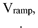
- the PWM quantizer 304 includes a ramp generator 402 that generates a sawtooth wave-shaped ramp voltage Vramp.
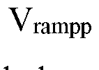
- the ramp voltage Vramp is a differential voltage pair comprising a positive ramp voltage Vrampp and negative ramp voltage Vrampm.
- the PWM quantizer 304 also includes a first switched-capacitor network (“SC Net.”) 404p and a second switched-capacitor network (“SC Net.”) 404n, each of which receives the positive and negative ramp voltages Vrampp and Vrampm.
- SC Net. switched-capacitor network
- the switched-capacitor network 404p/404n also receive a positive signal input voltage VIP and a negative signal input voltage VIM.
- the switched-capacitor network 404p/404n operate on the ramp voltages the signal input voltages VIP and VIM to generate respective
- the CEM block 408 generates a differential PWM output signal DPWM having a positive component denoted DPWM P and a negative component denoted Dpw Mn which are provided to the speaker driver 306 of Figure 3.
- the switched- capacitor network 404p/404n according to one embodiment are described in more detail with respect to Figure 7 below.
- FIG. 5 A a block diagram illustrating the composition of a combined linear gain KTOTAL of the quantizer 304 and driver 306 gain is shown.
- components that contribute to the combined linear gain KTOTAL include an analog gain KANA of the quantizer 304 (e.g., of switched capacitor network 404), a gain KDRV of the speaker driver 306, and a gain KCEM of the CEM block 408, as shown in Figure 5A and in equation (1) below.
- the combined gain KTOTAL of the quantizer 304 and driver 306 may be defined from linear analysis of the modulator 100 system as proportional to a product of the analog gain KANA, the driver gain KDRV, and the CEM gain KCEM.
- KTOTAL KANA * K DRV * K CEM (1)
- the driver gain KDRV is the ratio of the speaker voltage VSPK and the ramp voltage swing range Vramp(fd).
- the driver gain KDRV will be changed (assuming the ramp voltage swing range Vramp(fd) is maintained), and a change in the driver gain KDRV changes the combined gain KTOTAL.
- a change in the combined gain KTOTAL is undesirable because it changes the dynamics of the modulator 100 loop, e.g., changes the loop dynamics to be non-linear.
- Embodiments are described that advantageously, while maintaining a fixed combined gain KTOTAL, reduce the variation (or in some embodiments eliminate it) in the ramp voltage swing range Vramp ( fd ) and associated ramp slope between the two modes by adjusting the analog gain KANA of the quantizer 304, as shown in Figure 5B, to compensate for changes in the gain of the speaker driver 306 caused by a change of the speaker voltage VS PK values of the two modes.
- FIG. 7 a block diagram illustrating an embodiment of the quantizer 304 that enables the analog gain KANA to be adjusted in order to compensate for a change in the speaker voltage VS PK between operating modes is shown.
- the sawtooth wave- shaped ramp voltage V ramp is coupled to the comparator 406 through a switched capacitor network 404 (e.g., switched capacitor network 404 of Figure 4).
- the negative ramp voltage V rampm is coupled to the negative input of the comparator 406 through a switch controlled by a clock signal CLK f and then through a capacitor C2.
- the positive ramp voltage is coupled to the positive input of the
- comparator 406 through a switch controlled by clock signal CLK f and then through a capacitor C3.
- the node at the switch side of capacitor C2 is denoted node X
- the node at the switch side of capacitor C3 is denoted node Y.
- the other terminal of capacitor C2 is coupled to the negative ramp voltage V rampm through a switch controlled by a clock signal CLK r
- the other terminal of capacitor C3 is coupled to the positive ramp voltage through a switch controlled by clock signal CLK r .
- a common mode voltage V cm is also coupled to the positive and negative inputs of the comparator 406 through switches controlled by clock signal CLK r .
- the negative input to the comparator 406 is also coupled through a switch controlled by clock signal CLK f to a node that is coupled to a capacitor Cl and to positive signal input V IP through a switch controlled by clock signal CLK r .
- the positive input to the comparator 406 is also coupled through a switch controlled by clock signal CLK f to a node that is coupled to a capacitor C4 and to negative signal input V IM through a switch controlled by clock signal CLK r .
- the other terminal of capacitor Cl is coupled to node X, and the other terminal of capacitor C4 is coupled to node Y.
- Common mode voltage V cm is also coupled to node X and to node Y through switches controlled by a clock signal CLK r-hv .
- Negative signal input V IM is coupled to node X through a switch controlled by a clock signal CLK r -i v
- positive signal input V IP is coupled to node Y through a switch controlled by a clock signal CLK r-iv .
- the analog gain KANA has a gain value (first gain value) while operating in the HV mode (first mode) and a different gain value (second gain value) while operating in the LV mode (second mode), and the driver gain KDRV has a gain value (third gain value) while operating in the first mode and a different gain value (fourth gain value) while operating in the second mode, and the product of the first and third gain values is approximately the same as the product of the second and fourth gain values advantageously resulting in an approximately fixed combined gain KTOTAL across the two modes.
- controlling the respective analog gain KANA values of 0.5 and 1.0 accomplishes ramp voltage swing ranges Vramp(fd) of l .2vpp and 0.8vpp, respectively, for the two modes, which represents a significant reduction in the variation of the ramp voltage swing range V ramp(fd) over a conventional solution that does not adjust the analog gain KANA. More specifically, as shown in the table of Figure 6, the variation is advantageously reduced from a factor of 3 to a factor of 1.5.
- the analog gain KANA is adjustable by powers of two, yet the ratio of the speaker voltages VSPK may be non-powers of two, in which case the slope of the ramp voltage swing range V ramp(fd) may vary somewhat between the HV and LV modes; however, advantageously, the variation is significantly reduced with respect to a conventional amplifier not having the benefit of the variable analog gain KANA embodiments, and the benefits described may still be realized by the variable analog gain KANA embodiments.
- the analog gain KANA may be implemented to accomplish a non-power of two, as shown in the right-most column of the table of Figure 6 denoted LV (emb. 2).
- the ramp generator 902 includes an amplifier 904 having positive and negative inputs and positive and negative outputs. Coupled in parallel between the positive input and the negative output of the amplifier 904 are a first ramp capacitor C rampm and a first switch controlled by CLK rs t; additionally, coupled in parallel between the negative input and the positive output of the amplifier 904 are a second ramp capacitor C rampp and a second switch controlled by CLKrst. When the switches are open (e.g., CLK rs t is deasserted), two push-pull reference currents Iref (generated by current sources) are passing through the ramp capacitors Crampm and generating
- the reference current I ref is the quotient of a reference voltage Vref and a reference resistance R ref . Assertion of CLK rs t causes energy stored in the ramp capacitors C rampm and C rampp to dissipate causing the ramp voltages Vra mpp to be reset to a
- a resulting sawtooth wave is generated as the difference between the positive ramp voltage Vrampp and the negative ramp voltage Vrampm.
- a ramp voltage swing range Vramp(fd) is shown as the difference between the maximum value of Vrampp and the minimum value of Vrampm, which is also shown as the difference between the maximum value of the sawtooth wave and the common mode voltage V cm .
- a disadvantage of the prior art ramp generator 902 of Figures 9 and 10 that resets the sawtooth wave to the common mode voltage V cm is that it requires on each cycle a relatively wide reset time that is required to discharge the ramp capacitors Crampm and Crampp, which may reduce the modulation index (MI) associated with a PWM modulator that employs the ramp generator 902.
- MI modulation index
- Another disadvantage is that it requires the ramp voltages to reach relatively high voltage swing values.
- embodiments of an improved ramp generator are described below that address these disadvantages.
- FIG. 11 a block diagram illustrating a portion of a ramp generator 402 (e.g., ramp generator 402 of Figure 4) that employs a chopping technique to generate a triangular wave for use in a quantizer (e.g., quantizer 304 of Figure 3) of a PWM modulator (e.g., PWM modulator 100 of Figure 3) is shown.
- the ramp generator 402 includes an amplifier 1104 having positive and negative inputs and positive and negative outputs. Coupled between the positive input and the negative output of the amplifier 1104 is a ramp capacitor C rampm and coupled between the negative input and the positive output of the amplifier 1104 is a ramp capacitor Crampp.
- the ramp generator 402 also includes a chopping block 1106, or chopping switch 1106, whose first and second outputs are coupled to the positive and negative inputs of the amplifier 1104, respectively.
- the two inputs to the chopping switch 1106 are coupled to receive respective positive and negative reference currents I re fp and Irefm.
- the positive reference current I re fp is the quotient of positive reference voltage V re fp and a reference resistance R re f
- the negative reference current I re fm is the quotient of negative reference voltage V re fm and the reference resistance R re f.
- the chopping switch 1106 operates as a crossbar switch that may be dynamically controlled to operate in either a pass-through configuration or a cross configuration.
- the chopping switch 1106 connects the positive reference current I re f P to the positive input of the amplifier 1104 and the negative reference current I re fm to the negative input of the amplifier 1104. In the cross configuration, the chopping switch 1106 connects the positive reference current I re f P to the negative input of the amplifier 1104 and the negative reference current I re fm to the positive input of the amplifier 1104.
- the reference currents I re fp and Irefm selectively push-pull through the ramp capacitors C ra mpp and C ra mpm to generate respective negative and positive ramp voltages V ra mpm and V,-.-,m PP at the respective negative and positive outputs of the amplifier 1104, as described in more detail below.
- a common mode voltage V cm is selectively coupled to the positive and negative inputs of the amplifier 1104 through switches controlled by a clock signal CLK rs t.
- the node holding the negative ramp voltage V ra mpm is selectively coupled to the negative reference voltage Vrefm through a switch controlled by a clock signal CLK rs t 3 ⁇ 4 ii and is selectively coupled to the positive reference voltage V re fp through a switch controlled by a clock signal CLK rs t rise.
- the node holding the positive ramp voltage Vrampp is selectively coupled to the negative reference voltage Vrefm through a switch controlled by the clock signal CLK rs t rise and is selectively coupled to the positive reference voltage V re fp through a switch controlled by the clock signal CLK rs t f a ii.
- the ramp generator 402 also includes a de-chopping block 1108, or de-chopping switch 1108, whose first and second inputs are coupled to the negative and positive outputs of the amplifier 1104, respectively.
- the two outputs of the de-chopping switch 1108 are coupled to nodes that hold respective negative and positive output voltages V ou tm and V ou tp that may be provided to other portions of a quantizer (e.g., to switched capacitor network 404 for provision to comparator 406 of Figure 4 of quantizer 304 of Figure 3) for use in generating a PWM signal, e.g., for provision to a speaker driver (e.g., speaker driver 306 of Figure 3) for driving a speaker for audio generation.
- a quantizer e.g., to switched capacitor network 404 for provision to comparator 406 of Figure 4 of quantizer 304 of Figure 3
- a speaker driver e.g., speaker driver 306 of Figure 3
- the de-chopping switch 1108 operates as a crossbar switch that may be dynamically controlled to operate in either a pass-through configuration or a cross configuration, similar to the chopping switch 1106.
- the de-chopping switch 1108 connects the negative ramp voltage Vrampm to the negative output voltage Voutm node and the positive ramp voltage V,-.-,m PP to the positive output voltage Voutp node.
- the de-chopping switch 1108 connects the negative ramp voltage Vrampm to the positive output voltage Voutp node and the positive ramp voltage V r .-,m PP to the negative output voltage V ou tm node.
- FIG. 12 a timing diagram illustrating operation of the ramp generator 402 of Figure 11 is shown.
- CLK rs t is asserted to close the switches to apply the common mode voltage V cm to the inputs of the amplifier 1104.
- CLKrst fail is asserted to apply the negative reference voltage V re fm to the node holding the negative ramp voltage to apply the positive reference voltage V re fp to the node holding the positive
- the chopping switch 1106 is controlled to be in the cross configuration to connect the positive reference current I re f P to the negative input of the amplifier 1104 and to connect the negative reference current I re fm to the positive input of the amplifier 1104.
- the chopping switch 1106 is maintained in the cross configuration through the sampling period to cause the voltage across ramp capacitor C rampm to increase which increases the negative ramp voltage
- Vramp(fd) a positively sloping ramp voltage Vramp (shown in Figure 12 as a non-differential voltage Vrampm minus Vrampp) having a swing of approximately the difference between the positive reference voltage V re fp minus the negative reference voltage Vrefm, referred to as Vramp(fd), which is a first period of what will become a triangular wave, as shown.
- Vramp(fd) the de-chopping switch 1108 is controlled to be in the pass-through configuration to cause the negative ramp voltage V rampm to be provided as the negative output voltage Voutm and to cause the positive ramp voltage Vrampp to be provided as the positive output voltage V ou tp.
- the de-chopping switch 1108 in pass-through configuration results in the positively sloping ramp voltage Vramp of swing Vramp(fd) being passed through and provided on the output voltage VOUT, which is a first period of what will become a sawtooth wave, as shown.
- the ramp voltage Vramp is a negatively sloping ramp also having a swing of Vramp(fd) during the next sampling period, which will be polarity- inverted to form another positively sloping ramp of the sawtooth wave of the output voltage VOUT.
- This pattern repeats for subsequent sampling period pairs, resulting in a triangular wave ramp voltage Vramp, which is polarity-swapped on alternating periods (e.g., on periods in which the triangular wave ramp voltage negatively sloping) by the de-chopping switch 1 108 to form the sawtooth wave
- the ramp generator 402 advantageously enjoys the benefits perceived by smaller swings and reset times of the ramp capacitors, as described in more detail below.
- the chopping switch 1 106 is controlled to be in the pass-through configuration to connect the positive reference current I re fp to the positive input of the amplifier 1 104 and to connect the negative reference current I re fm to the negative input of the amplifier 1 104.
- the chopping switch 1 106 is maintained in the pass-through configuration through the second sampling period to cause the voltage across ramp capacitor C ra mpm to decrease which decreases the negative ramp voltage Vrampm from its positive peak to its negative peak and to cause the voltage across ramp capacitor C ra mpp to increase which increases the positive ramp voltage Vrampp from its negative peak to its positive peak, as shown.
- the de-chopping switch 1 108 is controlled to be in the cross configuration to cause the negative ramp voltage Vrampm to be provided as the positive output voltage Voutp and to cause the positive ramp voltage Vrampp to be provided as the negative output voltage Voutm.
- a negatively sloping ramp voltage Vramp is provided to the de- chopping switch 1 108 as a second period of a triangular wave having a swing of approximately Vramp(fd).
- the de-chopping switch 1 108 polarity- inverts the received negatively sloping ramp voltage Vra mp and provides the polarity-inverted version thereof as a positively sloping ramp having a swing of approximately V ra mp(fd) on the output voltage VOUT as a second period of the sawtooth wave.
- the de-chopping switch 1108 is controlled to be in the pass-through configuration to cause the positive ramp voltage V rampp to be provided as the positive output voltage Vou tp and to cause the negative ramp voltage Vrampm to be provided as the negative output voltage V outm .
- a positively sloping ramp voltage V ramp of a third period of a triangular wave is provided to and passed through by the de-chopping switch 1108 to provide a positively sloping ramp having a swing of approximately Vramp (fd) on the output voltage VOUT as a third period of the sawtooth wave.
- the purpose of the PWM modulator is to convert continuous voltage domain information into time domain information in which the time domain has a period T.
- a large reset time in the conventional ramp generator 902 of Figure 9 i.e., time required to reset the capacitors to the common mode voltage reduces the usable portion of the period T, which may result in a loss of dynamic range, for example.
- the large reset time may particularly exacerbate operation since it may detrimentally affect the ability to increase the duty cycle, for example.
- a sawtooth wave of swing Vramp(fd) (Vrefp minus V re fm) is provided on the output voltage VOU T of the ramp generator 402 similar to the sawtooth wave of Figure 10, which advantageously enables reuse of various system elements (e.g., comparator 406 or the switch capacitor network 404) with the added benefits of reduced capacitor reset time and swing values as a result of the manner in which the ramp generator 402 produces a sawtooth wave from an internally-generated triangular wave.
- the de-chopping switch 1108 provides a polarity-inverted version of the signal input V IN to the comparator 406 on alternating sampling periods, rather than a polarity- inverted version of the triangular wave, which may effectively accomplish a similar result.
- FIG 14 a block diagram illustrating a system for calibrating a gain of a quantizer (e.g., quantizer 304 of Figure 3) is shown.
- the system includes a ramp generator 402, switched capacitor network 404, and comparator 406 (e.g., of Figure 4).
- the system also includes a D flip-flop 1407 and a voltage reference generator 1405 that provides the reference voltage V re fp and Vrefm to the ramp generator 402.
- the ramp generator 402 provides the ramp voltage Vrampp and Vrampm to the switched capacitor network 404 which also receives the input signal V IP and V IM .
- the comparator 406 outputs a value Dp which is provides as the data input to the D flip-flop 1407.
- the output of the D flip-flop 1407 is value Deal.
- the D flip-flop 1407 is clocked by a calibration clock CLKcal.
- FIG. 15A through 15E timing diagrams illustrating aspects of gain calibration of the quantizer 304 of Figure 14 are shown.
- Process, voltage, and temperature variations may change the characteristics of the operation of the quantizer 304, such as the characteristics of the ramp generated by the ramp generator 402. The changes may be due to changes in the characteristics of the reference resistance R re f and ramp capacitance C ramp , for example.
- the ramp voltage as a function of time V ramp (t) is proportional to the ratio of the reference voltage V re f and the product of the reference resistance R re f and the ramp capacitance C ramp , as shown in equation (6).
- Gain calibration is performed in order to capture the gain error in the time domain and correct the gain error.
- V R, amp (t) (6) ref C ram p [0061]
- the common mode voltage V cm is connected to the signal inputs, and the comparator 406 compares the ramp voltage Vramp to the common mode voltage V cm .
- the calibration reference clock CLK cai causes the D flip-flop 1407 to latch the comparator 406 output Dp, as shown in Figure 15 A.
- the crossing occurs at the midpoint of the ramp. If the ramp slope is higher than normal (i.e., higher gain), a trim bit is changed in a step by step manner to reduce the slope of the ramp voltage Vramp until the polarity of D cai flips, as shown in Figure 15B. Conversely, if the ramp slope is lower than normal (i.e., lower gain), the trim bit is changed in a step by step manner to increase the slope of the ramp voltage the until the polarity of D cai flips, as shown in Figure
- the comparator 406 may have an offset which creates an error term on the gain calibration.
- the gain calibration process only looks for the crossing and perceives the offset as a gain error even when the slope of the ramp voltage Vmm p is correct. Adjusting to make the crossing mid-ramp creates an undesired gain error, shown in Figure 15D as an offset voltage Vos.
- the comparator 406 may have a time delay T d , shown in Figure 15E, which creates an error term on the gain calibration.
- the gain calibration process may perceive the time delay Td as a gain error even when the slope of the ramp voltage V ra mp is correct. More specifically, the delay error T d is treated like a voltage domain error. Adjusting to offset the time delay T d creates an undesired error in the slope of the ramp voltage as shown.
- FIG. 16 a block diagram illustrating an improved system for calibrating a gain of a quantizer (e.g., quantizer 304 of Figure 3) is shown.
- the system is similar in many respects to the system of Figure 14.
- the system of Figure 16 includes a chopping switch 1605 coupled between the output of the ramp generator 402 and the input of the switched capacitor network 404.
- the reference voltages V re fp and V re fm are passed through the ramp generator 402 to the chopping switch 1605 such that during the offset calibration process of quantizer 304, ramp voltages are not generated. That is, the ramp generator 402 is transparent to the reference voltages V refp and V refm .
- the chopping switch 1605 may operate in a pass-through configuration to connect the positive voltage reference V refp to the positive ramp voltage input of the switched capacitor network 404 and to connect the negative voltage reference V refm to the negative ramp voltage V rampm input.
- the chopping switch 1605 may operate in a cross configuration to connect the positive voltage reference V refp to the negative ramp voltage Vrampm input of the switched capacitor network 404 and to connect the negative voltage reference V refm to the positive ramp voltage V rampp input.
- the chopping switch 1605 is controlled by a clock signal CLK r ramp and CLK f ramp according to the normal operation of those signals within the ramp generator 402 as described with respect to Figure 13.
- the ramp voltage inputs to the switched capacitor network 404 are a chopped version of the reference voltage V refp and
- the common mode voltage V cm is connected to the signal inputs. Initially, higher than normal values of the reference voltage V refp and V refm are provided through the ramp generator 402 to the chopping switch 1605 and are scaled down over time until two consecutive values of the comparator 406 output Dp are the same, at which time the comparator 406 offset Vos is measured, as shown in the timing diagram of Figure 17A.
- FIG. 17B a timing diagram illustrating measurement of time delay T d of the comparator 406.
- the system set up is similar to that of the offset V os measurement. However, the smallest value of the reference voltage V refp and V refm is provided and remains fixed through the measurement process.
- the output Dp of comparator 406 is skewed from CLK r ramp by the comparator 406 delay T d .
- the calibration clock CLK cai whose rising edge is trimmable, retimes the comparator 406 output Dp.
- the rising edge of the calibration clock CLK cai starts from the rising edge of CLK r ramp and gets incremented.
- the delay T d is measured, as shown in Figure 17B.
- FIG. 17C a timing diagram illustrating calibration of the gain of the quantizer 304 is shown.
- the offset voltage Vos of comparator 406 measured according to the process described with respect to Figure 17A is applied to the reference voltage V refp and V refm to code shift them up or down.
- time delay T d of the comparator 406 measured according to the process described with respect to Figure 17B is applied to the calibration clock CLK cai to delay the edge of the calibration clock CLK cai to offset the effect of the comparator 406 delay T d .
- the gain error of the quantizer 304 e.g., the ramp slope
- non-ideal characteristics of the quantizer 304 may include the RC time constant used by the ramp generator to generate the ramp voltage; a bandgap used in a current source of the quantizer; a resistor, capacitor and/or transistor size ratio that controls a gain of the quantizer; a clock speed of the quantizer; and various circuit parasitic.
- These other non-ideal characteristics of the quantizer 304 may be measured in addition to, in place of, and/or in combination with the comparator 406 offset V os and time delay T d and adjusted for while the gain error of the quantizer 304 is calibrated.
- FIG. 18 a flowchart illustrating a method for calibrating a quantizer is shown. Operation begins at block 1802.
- a first non-ideality is measured (e.g., comparator offset V os per Figure 17A). The operation proceeds to block 1804.
- a second non-ideality is measured (e.g., comparator delay T d per Figure 17B). The operation proceeds to block 1806.
- additional non-idealities may be measured (e.g., RC time constant, current source bandgap, resistor/capaci tor/transistor size ratio clock speed). The operation proceeds to block 1808.
- the quantizer 304 is adjusted using the values of the non-idealities measured at blocks 1802 through 1806. The operation proceeds to block 1812.
- the gain of the quantizer 304 is calibrated while the quantizer 304 is adjusted using the non-ideality measured values.
- references in the appended claims to an apparatus or system or a component of an apparatus or system being adapted to, arranged to, capable of, configured to, enabled to, operable to, or operative to perform a particular function encompasses that apparatus, system, or component, whether or not it or that particular function is activated, turned on, or unlocked, as long as that apparatus, system, or component is so adapted, arranged, capable, configured, enabled, operable, or operative.
Landscapes
- Engineering & Computer Science (AREA)
- Power Engineering (AREA)
- Theoretical Computer Science (AREA)
- Multimedia (AREA)
- Microelectronics & Electronic Packaging (AREA)
- Amplifiers (AREA)
- Physics & Mathematics (AREA)
- Spectroscopy & Molecular Physics (AREA)
- Computer Networks & Wireless Communication (AREA)
- Signal Processing (AREA)
- Nonlinear Science (AREA)
- Analogue/Digital Conversion (AREA)
Abstract
Description





Claims
Priority Applications (3)
| Application Number | Priority Date | Filing Date | Title |
|---|---|---|---|
| GB2104544.8A GB2590585B (en) | 2018-10-14 | 2019-09-30 | Chopped triangular wave PWM quantizer |
| CN201980067772.8A CN113016138B (en) | 2018-10-14 | 2019-09-30 | A chopped triangular wave PWM quantizer and a PWM modulator with a controllable analog gain and a quantizer that can be calibrated for multiple non-ideal gains affecting characteristics |
| KR1020217011107A KR102690263B1 (en) | 2018-10-14 | 2019-09-30 | PWM modulator with chopping triangle wave PWM quantizer and quantizer with controllable analog gain and correctable for characteristics affecting multi-non-ideal gain |
Applications Claiming Priority (6)
| Application Number | Priority Date | Filing Date | Title |
|---|---|---|---|
| US201862745457P | 2018-10-14 | 2018-10-14 | |
| US62/745,457 | 2018-10-14 | ||
| US16/163,638 US10659029B2 (en) | 2018-10-14 | 2018-10-18 | Chopped triangular wave PWM quantizer |
| US16/163,638 | 2018-10-18 | ||
| US16/163,766 | 2018-10-18 | ||
| US16/163,766 US10819328B2 (en) | 2018-10-14 | 2018-10-18 | PWM modulator having quantizer with controllable analog gain and calibratable for multi-non-ideal gain-affecting characteristics |
Publications (1)
| Publication Number | Publication Date |
|---|---|
| WO2020081220A1 true WO2020081220A1 (en) | 2020-04-23 |
Family
ID=70159143
Family Applications (1)
| Application Number | Title | Priority Date | Filing Date |
|---|---|---|---|
| PCT/US2019/053735 Ceased WO2020081220A1 (en) | 2018-10-14 | 2019-09-30 | Chopped triangular wave pwm quantizer and pwm modulator having quantizer with controllable analog gain and calibratable for multi-non-ideal gain-affecting characteristics |
Country Status (5)
| Country | Link |
|---|---|
| US (3) | US10659029B2 (en) |
| KR (1) | KR102690263B1 (en) |
| CN (1) | CN113016138B (en) |
| GB (3) | GB2610918B (en) |
| WO (1) | WO2020081220A1 (en) |
Families Citing this family (5)
| Publication number | Priority date | Publication date | Assignee | Title |
|---|---|---|---|---|
| US10659029B2 (en) | 2018-10-14 | 2020-05-19 | Cirrus Logic, Inc. | Chopped triangular wave PWM quantizer |
| TWI674770B (en) * | 2019-01-18 | 2019-10-11 | 瑞昱半導體股份有限公司 | Sigma-delta analog-to-digital converter capable of reducing idle tones while alternately conducting signal conversion and comparator offset calibration |
| US12120797B2 (en) * | 2019-09-06 | 2024-10-15 | Signify Holding, B.V. | Power supply device, a power receiving device and power supply and receipt methods |
| CN113917837B (en) * | 2021-09-15 | 2024-04-19 | 南京晨光集团有限责任公司 | Digital electrohydraulic proportional servo valve command signal conditioning method |
| CN116599500B (en) * | 2023-07-17 | 2023-11-03 | 上海海栎创科技股份有限公司 | Voltage gain signal detection device and method |
Citations (1)
| Publication number | Priority date | Publication date | Assignee | Title |
|---|---|---|---|---|
| EP1788701A1 (en) * | 2005-11-17 | 2007-05-23 | STMicroelectronics S.r.l. | Class-D audio amplifier |
Family Cites Families (24)
| Publication number | Priority date | Publication date | Assignee | Title |
|---|---|---|---|---|
| US1039672A (en) | 1912-04-17 | 1912-09-24 | Titanium Alloy Mfg Co | Compound or composition of matter and method of producing same. |
| US5559467A (en) | 1995-01-27 | 1996-09-24 | The Regents Of The University Of California | Digital, pulse width modulation audio power amplifier with noise and ripple shaping |
| US5537027A (en) * | 1995-04-25 | 1996-07-16 | Analog Devices, Inc. | Calibration system for an asymmetrical ramp generator system |
| DE69635626T2 (en) * | 1995-05-26 | 2006-10-26 | Rambus Inc., Los Altos | Phase shifter for use in a quadrature clock generator |
| US5719528A (en) * | 1996-04-23 | 1998-02-17 | Phonak Ag | Hearing aid device |
| US6404251B1 (en) * | 2000-03-27 | 2002-06-11 | Linear Technology Corporation | Systems and methods for linearly varying a pulse-width modulation signal with a control signal |
| US6636124B1 (en) * | 2001-11-30 | 2003-10-21 | Analog Technologies, Inc. | Method and apparatus for accurate pulse width modulation |
| US6784710B2 (en) * | 2002-12-11 | 2004-08-31 | Cirrus Logic, Inc. | Multistage pulse width modulator |
| US6998910B2 (en) * | 2004-01-22 | 2006-02-14 | Texas Instruments Incorporated | Amplifier using delta-sigma modulation |
| US7146283B2 (en) * | 2004-08-16 | 2006-12-05 | National Instruments Corporation | Calibrating analog-to-digital systems using a precision reference and a pulse-width modulation circuit to reduce local and large signal nonlinearities |
| US7262658B2 (en) * | 2005-07-29 | 2007-08-28 | Texas Instruments Incorporated | Class-D amplifier system |
| EP1804374A3 (en) * | 2005-12-27 | 2008-05-28 | Sharp Kabushiki Kaisha | Switching amplifier |
| US7414471B2 (en) * | 2006-06-06 | 2008-08-19 | Texas Instruments Incorporated | Common-mode technique for a digital I/P class D loop |
| JP4833812B2 (en) * | 2006-11-30 | 2011-12-07 | パナソニック株式会社 | PWM drive device and output offset correction method thereof |
| US7554473B2 (en) * | 2007-05-02 | 2009-06-30 | Cirrus Logic, Inc. | Control system using a nonlinear delta-sigma modulator with nonlinear process modeling |
| JP2012015650A (en) * | 2010-06-29 | 2012-01-19 | Renesas Electronics Corp | Class-d amplifier |
| EP3229371B1 (en) * | 2016-04-06 | 2020-03-11 | Nxp B.V. | Audio amplifier system |
| US10581422B2 (en) * | 2016-09-09 | 2020-03-03 | Kabushiki Kaisha Toshiba | PWM modulator |
| CN206743199U (en) * | 2017-03-06 | 2017-12-12 | 恩平市奥达电子科技有限公司 | A kind of high power audio-frequency power amplifier |
| US10067478B1 (en) * | 2017-12-11 | 2018-09-04 | Silicon Laboratories Inc. | Use of a recirculating delay line with a time-to-digital converter |
| US10396724B1 (en) * | 2018-05-30 | 2019-08-27 | Semiconductor Components Industries, Llc | Amplifier with common mode loop and chop |
| US11115046B2 (en) * | 2018-06-11 | 2021-09-07 | Cirrus Logic, Inc. | Closed loop control in a camera module |
| US10476444B1 (en) * | 2018-09-26 | 2019-11-12 | Cirrus Logic, Inc. | Cross-fading in dual-path pulse width modulation system |
| US10659029B2 (en) | 2018-10-14 | 2020-05-19 | Cirrus Logic, Inc. | Chopped triangular wave PWM quantizer |
-
2018
- 2018-10-18 US US16/163,638 patent/US10659029B2/en active Active
- 2018-10-18 US US16/163,766 patent/US10819328B2/en active Active
-
2019
- 2019-09-30 GB GB2210457.4A patent/GB2610918B/en active Active
- 2019-09-30 GB GB2210456.6A patent/GB2610917B/en active Active
- 2019-09-30 GB GB2104544.8A patent/GB2590585B/en active Active
- 2019-09-30 KR KR1020217011107A patent/KR102690263B1/en active Active
- 2019-09-30 WO PCT/US2019/053735 patent/WO2020081220A1/en not_active Ceased
- 2019-09-30 CN CN201980067772.8A patent/CN113016138B/en active Active
-
2020
- 2020-08-18 US US16/996,779 patent/US11296685B2/en active Active
Patent Citations (1)
| Publication number | Priority date | Publication date | Assignee | Title |
|---|---|---|---|---|
| EP1788701A1 (en) * | 2005-11-17 | 2007-05-23 | STMicroelectronics S.r.l. | Class-D audio amplifier |
Non-Patent Citations (2)
| Title |
|---|
| MASAAKI SASAKI ET AL: "A Wide-Dynamic-Range CMOS Image Sensor Based on Multiple Short Exposure-Time Readout With Multiple-Resolution Column-Parallel ADC", IEEE SENSORS JOURNAL, IEEE SERVICE CENTER, NEW YORK, NY, US, vol. 7, no. 1, 1 January 2007 (2007-01-01), pages 151 - 158, XP011152878, ISSN: 1530-437X, DOI: 10.1109/JSEN.2006.888058 * |
| WITTMANN JUERGEN ET AL: "A configurable sawtooth based PWM generator with 2 ns on-time for >50 MHz DCDC converters", 2015 11TH CONFERENCE ON PH.D. RESEARCH IN MICROELECTRONICS AND ELECTRONICS (PRIME), IEEE, 29 June 2015 (2015-06-29), pages 41 - 44, XP033200746, DOI: 10.1109/PRIME.2015.7251089 * |
Also Published As
| Publication number | Publication date |
|---|---|
| GB2610917B (en) | 2023-06-07 |
| US10819328B2 (en) | 2020-10-27 |
| GB2610917A (en) | 2023-03-22 |
| US20210044285A1 (en) | 2021-02-11 |
| GB202104544D0 (en) | 2021-05-12 |
| GB2590585B (en) | 2023-03-29 |
| CN113016138A (en) | 2021-06-22 |
| US20200119702A1 (en) | 2020-04-16 |
| GB2610918A (en) | 2023-03-22 |
| GB202210456D0 (en) | 2022-08-31 |
| KR20210090166A (en) | 2021-07-19 |
| GB2590585A (en) | 2021-06-30 |
| CN113016138B (en) | 2022-07-15 |
| GB202210457D0 (en) | 2022-08-31 |
| GB2610918B (en) | 2023-06-07 |
| US20200119725A1 (en) | 2020-04-16 |
| KR102690263B1 (en) | 2024-07-31 |
| US11296685B2 (en) | 2022-04-05 |
| US10659029B2 (en) | 2020-05-19 |
Similar Documents
| Publication | Publication Date | Title |
|---|---|---|
| US11050433B1 (en) | Using a tracking switched-mode power supply to increase efficiency of a current digital-to-analog converter-based output stage | |
| US11296685B2 (en) | PWM modulator having quantizer calibratable for multi-non-ideal gain-affecting characteristics | |
| US11290069B2 (en) | Distortion reducing variable output impedance class-D amplifier | |
| US10008994B2 (en) | Audio amplifier system | |
| CN107623495B (en) | Low noise circuit | |
| US9917557B1 (en) | Calibration for amplifier with configurable final output stage | |
| US11750157B2 (en) | Common-mode leakage error calibration for current sensing in a Class-D stage using a pilot tone | |
| CN110582935B (en) | Switching in audio systems with multiple playback paths | |
| CN109004936B (en) | Digital-analog converter and digital power amplifier subsystem | |
| GB2564721A (en) | Reducing audio artifacts in an amplifier with configurable final output stage | |
| WO2017160556A1 (en) | Generation of voltage reference signals in a hybrid switched mode amplifier | |
| CN110603731B (en) | Switching in Amplifiers with Configurable Final Output Stages | |
| CN208433953U (en) | A kind of digital analog converter and digital power amplifier subsystem | |
| US20250219600A1 (en) | Amplification device and operation method thereof | |
| US20250219603A1 (en) | Amplifying circuit and amplifying device | |
| GB2564720A (en) | Reducing audio artifacts in an amplifier with configurable final output stage | |
| GB2550026A (en) | Generation of voltage reference signals in a hybrid switched mode amplifier |
Legal Events
| Date | Code | Title | Description |
|---|---|---|---|
| 121 | Ep: the epo has been informed by wipo that ep was designated in this application |
Ref document number: 19802326 Country of ref document: EP Kind code of ref document: A1 |
|
| ENP | Entry into the national phase |
Ref document number: 202104544 Country of ref document: GB Kind code of ref document: A Free format text: PCT FILING DATE = 20190930 |
|
| WWE | Wipo information: entry into national phase |
Ref document number: 2104544.8 Country of ref document: GB |
|
| ENP | Entry into the national phase |
Ref document number: 20217011107 Country of ref document: KR Kind code of ref document: A |
|
| NENP | Non-entry into the national phase |
Ref country code: DE |
|
| 122 | Ep: pct application non-entry in european phase |
Ref document number: 19802326 Country of ref document: EP Kind code of ref document: A1 |
|
| WWD | Wipo information: divisional of initial pct application |
Ref document number: 2104544.8 Country of ref document: GB Ref document number: 2210457.4 Country of ref document: GB |
|
| WWP | Wipo information: published in national office |
Ref document number: 2210457.4 Country of ref document: GB Ref document number: 2210456.6 Country of ref document: GB |
|
| WWG | Wipo information: grant in national office |
Ref document number: 2104544.8 Country of ref document: GB |
|
| WWG | Wipo information: grant in national office |
Ref document number: 2210457.4 Country of ref document: GB Ref document number: 2210456.6 Country of ref document: GB |