WO2020045273A1 - アンテナコイルの設計方法およびそのプログラム - Google Patents
アンテナコイルの設計方法およびそのプログラム Download PDFInfo
- Publication number
- WO2020045273A1 WO2020045273A1 PCT/JP2019/033009 JP2019033009W WO2020045273A1 WO 2020045273 A1 WO2020045273 A1 WO 2020045273A1 JP 2019033009 W JP2019033009 W JP 2019033009W WO 2020045273 A1 WO2020045273 A1 WO 2020045273A1
- Authority
- WO
- WIPO (PCT)
- Prior art keywords
- antenna
- antenna coil
- designed
- coil
- meshes
- Prior art date
- Legal status (The legal status is an assumption and is not a legal conclusion. Google has not performed a legal analysis and makes no representation as to the accuracy of the status listed.)
- Ceased
Links
Images







Classifications
-
- H—ELECTRICITY
- H02—GENERATION; CONVERSION OR DISTRIBUTION OF ELECTRIC POWER
- H02J—ELECTRIC POWER NETWORKS; CIRCUIT ARRANGEMENTS OR SYSTEMS FOR SUPPLYING OR DISTRIBUTING ELECTRIC POWER; SYSTEMS FOR STORING ELECTRIC ENERGY
- H02J50/00—Circuit arrangements or systems for wireless supply or distribution of electric power
- H02J50/40—Circuit arrangements or systems for wireless supply or distribution of electric power using two or more transmitting or receiving devices
-
- G—PHYSICS
- G06—COMPUTING OR CALCULATING; COUNTING
- G06F—ELECTRIC DIGITAL DATA PROCESSING
- G06F30/00—Computer-aided design [CAD]
- G06F30/10—Geometric CAD
-
- G—PHYSICS
- G06—COMPUTING OR CALCULATING; COUNTING
- G06F—ELECTRIC DIGITAL DATA PROCESSING
- G06F30/00—Computer-aided design [CAD]
- G06F30/20—Design optimisation, verification or simulation
-
- H—ELECTRICITY
- H02—GENERATION; CONVERSION OR DISTRIBUTION OF ELECTRIC POWER
- H02J—ELECTRIC POWER NETWORKS; CIRCUIT ARRANGEMENTS OR SYSTEMS FOR SUPPLYING OR DISTRIBUTING ELECTRIC POWER; SYSTEMS FOR STORING ELECTRIC ENERGY
- H02J50/00—Circuit arrangements or systems for wireless supply or distribution of electric power
- H02J50/10—Circuit arrangements or systems for wireless supply or distribution of electric power using inductive coupling
- H02J50/12—Circuit arrangements or systems for wireless supply or distribution of electric power using inductive coupling of the resonant type
Definitions
- the present invention relates to wireless power supply, and more particularly, to a technology for designing an antenna coil.
- Wireless power transmission can be broadly divided into near-field type and far-field type.
- the near-field type is a method of transmitting power by connecting a power transmission side and a power reception side via a magnetic field or an electric field, and can transmit large power with high efficiency, but has a short transmission distance.
- the far-field type is a method of receiving power by capturing and rectifying energy emitted as an electromagnetic wave by an antenna, and is capable of long-distance transmission, but has low transmission efficiency.
- the Wireless Power Consortium was established in 2008, an industry group that established international standards, and in 2010, the first international standard for wireless power supply, Qi, was formulated. Initially, it was designed to support low power of 5 W or less, but in 2015 a standard was established that supports up to 15 W. At present, the AirFuelAlliance, a standardization organization following WPC, has established a standard of up to 50W.
- the electromagnetic induction type has a feature that the transmission distance is limited to several centimeters and is susceptible to misalignment. Therefore, it has more significance as a non-contact power supply terminal than wireless power transmission.
- the magnetic resonance coupling type solves the problem of the electromagnetic induction type because it has features such as medium-range and high-efficiency transmission, resistance to misalignment, and simple expansion of the transmission distance by a relay coil. .
- FIG. 1 is a block diagram of a magnetic resonance coupling type wireless power supply system.
- the wireless power supply system 2 includes a power transmitting device (power @ transmitter) 10 and a power receiving device (power @ receiver) 20.
- a repeater that relays electric power is provided between the power transmitting device 10 and the power receiving device 20.
- the power transmission device 10 includes a power transmission coil L TX , a resonance capacitor C TX, and a drive circuit 12.
- the drive circuit 12 generates a magnetic field by passing an alternating current through the coil L TX on the power transmission side and exciting the coil, as in the principle of the electromagnetic induction method, and induces a current by capturing the magnetic field with the power receiving coil L RX . Transmit power.
- the power receiving device 20 includes a power receiving coil L RX , a resonance capacitor C RX, and a load 22.
- Load 22 including a rectifier circuit for rectifying an alternating current to flow in the receiving coil L RX.
- the magnetic resonance coupling type which resonates the magnetic field, has features such as medium-distance and high-efficiency transmission, resistance to misalignment, and easy expansion of the transmission distance using relay coils. It is being actively performed.
- the magnetic resonance coupling type is expected to be applied to various applications.
- FIGS. 2A and 2B are equivalent circuit diagrams of the wireless power supply system 2.
- the power transmission coil L TX and receiving coil L RX is coupled with mutual inductance L M. It is known that such a pair of power transmission and reception coils is represented by a T-type equivalent circuit as shown in FIG.
- the maximum transmission efficiency ⁇ max of wireless power is expressed by Expression (1) using the product of the coupling coefficient k and the quality coefficient Q.
- FIG. 3 is a diagram showing the maximum efficiency with k 2 Q 1 Q 2 as a parameter.
- the coupling coefficient k or the quality coefficient Q is used as a performance index of the resonator.
- the resonance improves the efficiency by increasing the quality factor Q value.
- the design of a resonator used in a real environment relies on experience, and optimization by cut and try is required. This is because the transmission efficiency depends on innumerable parameters such as the shape, size, number of turns, and pitch of the resonator, and metal pieces and electronic components of the power receiving device exist around the resonator, and loss in surrounding materials is reduced. This is because it occurs. Therefore, when designing the resonator, the parameters are adjusted by paying sufficient attention to these operating environments, and there is a problem that the design cost increases.
- the present invention has been made in such a situation, and one of the exemplary purposes of one embodiment of the present invention is to provide a technique for reducing the effort of trial and error design when designing an antenna coil.
- the antenna coil design method includes a step of modeling a surrounding environment including a pair of antenna coils, a step of dividing a space in which an antenna to be designed is to be arranged into a plurality of meshes, and an optimization of each mesh in the modeled surrounding environment. And calculating the shape of the antenna coil to be designed from the current distribution of the plurality of meshes.
- the antenna coil design method includes a step of modeling a surrounding environment including a pair of antenna coils, a step of dividing a space in which an antenna to be designed is to be arranged into a plurality of meshes, and an optimization of each mesh in the modeled surrounding environment. Calculating the magnetic dipole moment of the plurality of meshes, obtaining contour lines of the distribution of magnetic dipole moments of the plurality of meshes, and obtaining the shape of the antenna coil based on the contour lines.
- antenna design can be simplified. Can be provided.
- FIG. 1 is a block diagram of a magnetic resonance coupling type wireless power feeding system.
- 2A and 2B are equivalent circuit diagrams of the wireless power supply system.
- the k 2 Q 1 Q 2 is a diagram showing the maximum efficiency as parameters. It is a flowchart of the automatic design method of an antenna coil. It is a figure explaining a subdivided conductor mesh.
- FIG. 2 is a diagram illustrating a model of a wireless power supply system to be designed. It is a figure explaining the influence to Z matrix by sharing a conductor. It is a figure showing an example of the derived current distribution.
- FIG. 4 is a diagram illustrating a magnetic dipole moment in a minute region.
- FIG. 9 is a diagram illustrating an example of a magnetic dipole moment distribution derived from the current distribution in FIG. 8.
- FIGS. 11A and 11B are diagrams showing an example of the shape of the antenna coil obtained from the distribution of the magnetic dipole moment in FIG.
- FIG. 3 is an equivalent circuit diagram of a wireless power supply system including a plurality of transmission-side resonators. It is an equivalent circuit diagram of a transmission circuit.
- FIG. 4 is an equivalent circuit diagram illustrating dispersion reactance compensation.
- FIG. 3 is a diagram showing uniform current distribution by dispersion reactance compensation.
- the wireless power supply system 2 forms a resonator including a power transmission device 10 and a power reception device 20.
- a coil an automatic design method of an antenna coil (hereinafter, simply referred to as a coil) forming the resonator will be described.
- Coil L1 of automatic design object, the power transmission is one of a coil L TX and receiving coil L RX, the information such as the shape of the other (antenna coil L2 of the pair) to be known.
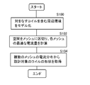
- FIG. 4 is a flowchart of an automatic antenna coil design method. This design method is embodied by a software program, which is loaded into a memory of a computer and causes a computer (specifically, a CPU) to execute each processing shown in the flowchart.
- a software program which is loaded into a memory of a computer and causes a computer (specifically, a CPU) to execute each processing shown in the flowchart.
- the surrounding environment including the coil L2 forming a pair is modeled (S100).
- the surrounding environment includes, in addition to the antenna coil L2, various metal and dielectric components existing around the antenna coil L2 and the coil L1 to be designed. For example, it is rare that the antenna coils L1 and L2 are exposed to space, and are usually covered with a dielectric cover. In this case, the surrounding environment includes the cover.
- the space in which the coil L1 to be designed is to be arranged is divided into a plurality of meshes, and the optimal current amount of each mesh in the modeled surrounding environment is calculated (S102).
- the space may be a two-dimensional plane or a three-dimensional space.
- the shape of the coil L1 to be designed is obtained from the current distribution of the plurality of meshes (S104).
- the paired resonator indicates a power receiving coil (power transmitting coil) if the design target is a power transmitting coil (power receiving coil).
- the efficiency is defined by the power efficiency.
- the loss is not considered in the RF inverter and the rectifier circuit, but is analyzed based on the coupling between the coils and the loss in the surrounding material.
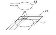
- FIG. 5 is a diagram for explaining the subdivided conductor mesh.
- the antenna coil L1 to be designed is provided at a position facing the pair of antenna coils L2.
- the antenna coil L1 forming a pair is simply shown as a loop coil having one turn.
- the space 30 in which the antenna coil L1 to be designed is to be incorporated is divided into a plurality of meshes.
- the space 30 is a plane with a negligible thickness, and in the drawing, it is assumed that there is no current component in a direction orthogonal to the coil surface of the antenna.
- the plane 30 has a conductor mesh 32 that is finely divided so as to approximate a conductor surface.
- the size of the conductor mesh 32 may be determined in consideration of the amount of calculation, required calculation accuracy, and the like. For example, the size is arranged in a 100 ⁇ 100, 50 ⁇ 50, 10 ⁇ 10 matrix.
- the mesh is not limited to a square, but may be rectangular according to the shape of the area where the antenna coil is set. Therefore, a matrix-like conductor mesh such as 50 ⁇ 100 may be employed.
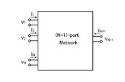
- FIG. 6 is a diagram illustrating a model of the wireless power supply system to be designed.
- N pieces of circular currents I 1 ⁇ I N is regarded as the N loop coil.
- a paired resonator is included, it can be considered as an N + 1 port circuit network. Therefore, the Z matrix of the (N + 1) th port is calculated using an electromagnetic field simulation or an equivalent circuit analysis, and the optimum current distribution is calculated using the Z matrix.
- MISO Multiple-Input-Single-Output
- FIG. 7 is a diagram for explaining the effect on the Z matrix by sharing a conductor.
- the impedance z included in both the loop i and the adjacent loop j is incorporated into Z as -z because the direction of the current flowing through the shared side is opposite.
- the matrix R of the conductor mesh is represented by the following equation.
- r ij is a resistance component of a conductor portion shared by adjacent loops i and j.
- the conductor mesh, the pair of antenna coils and the surrounding environment can be regarded as a passive network that does not include a power supply therein, the power consumption caused by an arbitrary current vector I is always non-negative. Therefore, the matrix R satisfies Equation (3) for any real vector I.
- the matrix R is a semi-definite value. That is, the current distribution of the loop coil that maximizes the efficiency in the conductor mesh can be obtained in the same manner as the efficiency maximization problem in the MISO system.
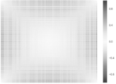
- FIG. 8 is a diagram showing an example of the derived current distribution.
- a positive (negative) value indicates a right (left) direction
- a positive (negative) value in a vertical direction indicates an upward (down) direction.
- the magnetic field at position r can be represented using a magnetic dipole moment.
- the magnetic dipole moment m is a vector d having a magnitude of the distance d between the magnetic poles, assuming a pair of positive and negative magnetic poles in which the magnitude of the magnetic charge is equal to q m and the positive magnetic charge is turned from the negative magnetic charge. And is defined as equation (4).
- the magnetic field B (r) is represented by Expression (5) using the magnetic dipole moment.
- loops with the same magnitude of magnetic dipole moment can be reproduced collectively by passing an appropriate current through a single loop surrounding them, and the current at that time is the area of the region Equation (7) can be obtained from the relationship between the magnitude of the magnetic dipole moment of each loop and the magnitude.
- S i is the area of the region surrounding loop
- m i is the magnetic dipole moment magnitude to produce a loop in the enclosed area
- mu 0 denotes the permeability of vacuum.
- FIG. 10 is a diagram showing an example of the distribution of the magnetic dipole moment derived from the current distribution in FIG.
- the contour of the resonator is presented by using the contour of the distribution of the magnetic dipole moment. Note that contour lines are drawn for each
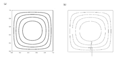
- FIGS. 11A and 11B are diagrams showing an example of the shape of the antenna coil obtained from the distribution of the magnetic dipole moment in FIG.
- the outline of the antenna coil is determined using the contour line of the magnetic dipole moment, and the number of turns of the coil is set to five.
- the shape of the antenna coil may be defined so as to follow the contour line.
- the antenna coil is finally formed. Can be designed as a single conductor as shown in FIG.
- the shape of the antenna coil derived by this design method is compared with the transmission efficiency of a coil shape that is generally considered to have high efficiency.
- the transmission efficiency is compared by the kQ product.
- FIGS. 12A and 12B are equivalent circuit diagrams of the wireless power supply system 2 including a plurality of transmission-side resonators.
- a number of resonators on the transmission side are combined as one resonator.
- the physical shape of an antenna is limited by frequency. This recognition is the same not only for the radiation type antenna but also for the resonator used in the magnetic resonance coupling type wireless power transmission. When the operating frequency is high and the resonator shape is large, the current distribution is biased, and sometimes the direction of the current is reversed inside the resonator. At this time, the magnetic field cancels out in the resonator, which leads directly to a decrease in the Q value, which is a performance index of the resonator.
- the non-uniformity of the current distribution is the reason for adjusting the parameters of the resonator design by trial and error. Also in this design method, it is assumed that the current flowing through one conductor (antenna coil) is uniform. Therefore, the applicable resonator shape may be limited to a range that can be regarded as electrically small. If the non-uniformity of the current distribution can be improved, the applicable range of the present design method will be greatly expanded.
- FIGS. 13A and 13B are equivalent circuit diagrams of lossy and lossless transmission circuits. Let L be the inductance per unit length, C be the capacitance per unit length, and R and G be the loss components associated with L and C, respectively. When R and G can be considered to be sufficiently small, a lossless line is obtained as shown in FIG.
- Non-Patent Document 3 DRC: Distributed ⁇ Reacquantance ⁇ Compensation
- This distributed reactance compensation was originally proposed as a technique for reducing the magnetic field strength around the antenna coil and reducing the dielectric loss by inserting a reactance compensation capacitor not only in the input port but also in the antenna coil.
- CRC Concentrated Reacquantance Compensation
- distributed reactance compensation realizes a resonance state in the coil by inserting a large number of capacitances in the antenna coil and reduces the voltage difference between lines. As a result, the charge stored in the parasitic capacitor is reduced.
- the present inventors have found that the distributed reactance compensation not only reduces the dielectric loss but also makes the current distribution of the antenna coil uniform. This phenomenon should not be regarded as a known technique.
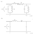
- FIG. 14 is an equivalent circuit diagram for explaining the distributed reactance compensation.
- the antenna coil is divided into a plurality of elements, and a compensating capacitor is inserted between them.
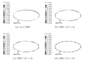
- FIGS. 15A to 15D are diagrams showing simulation results of current distribution by dispersion reactance compensation.
- the current distribution of the loop coil having a diameter of 5 m at an operating frequency of 6.78 MHz was calculated by an electromagnetic field simulation.
- the wire diameter of the loop coil was 1 mm, the material was copper, and FEKO manufactured by Altair Inc. was used for the simulator.
- FIG. 15A shows a case without compensation. No distributed reactance compensation is performed, and a reactance compensation capacitor is connected to the input port.
- the current distribution is normalized by the maximum value in the resonator.
- the current intensity is minimum at the input port portion, and is about 30% of the current intensity as compared with the portion farthest from the port. This result indicates that at an operating frequency of 6.78 MHz, even with an antenna having one turn, the current distribution can be greatly distorted, and the distortion of the current distribution further increases as the number of turns increases.
- FIGS. 15B to 15D show simulation results when dispersion reactance compensation is performed.
- the number N of capacitors used for dispersion reactance compensation is three, two, four, and eight.
- the intensity and direction of the current in each capacitor and the current flowing through the input port are equal.
- the capacitance at which the current distribution becomes uniform is considered.
- the factors that make the current distribution uniform by dispersion reactance compensation can be considered by transmission line theory.
- the conductor in the resonator is viewed as a kind of transmission line, the current distribution becomes non-uniform because charges are stored in a parasitic capacitor existing between the lines. It is considered that the distributed reactance compensation reduces the potential difference between the lines by arranging a large number of capacitances in the resonator, so that the charge stored in the parasitic capacitor is reduced and the current distribution is made uniform.
- the current distribution of the antenna coil can be made uniform. Therefore, it is preferable to incorporate dispersion reactance compensation into a software program using this design method when designing an antenna used in a frequency band of several MHz or more.
- the shape of the antenna coil is determined by the above-described design method. Then, additional processing related to dispersion compensation is performed on the antenna coil.
- the number N of capacitors to be inserted may be specified manually, or the non-uniformity of the current without compensation is calculated as shown in FIG. The number N may be determined.
- the S parameter (Z parameter) when it is regarded as a transmission line can be calculated.
- the capacitance value of the capacitor to be inserted can be calculated by solving equation (11) using the Z parameter.
- the present invention can be used for wireless power supply.
- Wireless power supply system 10 Power transmission device 20 Power reception device L TX power transmission coil C TX resonance capacitor L RX power reception coil C RX resonance capacitor
Landscapes
- Engineering & Computer Science (AREA)
- Physics & Mathematics (AREA)
- Theoretical Computer Science (AREA)
- General Physics & Mathematics (AREA)
- Geometry (AREA)
- Evolutionary Computation (AREA)
- Computer Hardware Design (AREA)
- General Engineering & Computer Science (AREA)
- Computer Networks & Wireless Communication (AREA)
- Power Engineering (AREA)
- Pure & Applied Mathematics (AREA)
- Mathematical Optimization (AREA)
- Mathematical Analysis (AREA)
- Computational Mathematics (AREA)
- Charge And Discharge Circuits For Batteries Or The Like (AREA)
Abstract
設計対象のアンテナコイルと対を成すアンテナコイルを含む周囲環境をモデル化する(S100)。そして設計対象のアンテナを配置すべき空間を複数のメッシュに区切り、各メッシュの最適な電流量を計算する(S102)。そして、複数のメッシュの電流分布から設計対象のアンテナコイルの形状を取得する(S104)。
Description
本発明は、無線給電に関し、特にアンテナコイルの設計技術に関する。
無線電力伝送は近傍界型と遠方界型に大別することができる。近傍界型は、磁界や電界を介して送電側と受電側を結びつけることで電力を送る手法であり、大きな電力を高効率で伝送することが可能であるが、伝送距離が短い。一方、遠方界型は、電磁波として飛ばしたエネルギーをアンテナで捕捉・整流することで電力を受け取る手法であり、長距離の伝送が可能であるが、伝送効率は低い。
家電機器やスマートフォン、電気自動車への給電を行う場合、数十Wから数kWという比較的大きな電力が必要なため、近傍界方式である、電磁誘導方式、もしくは磁界共振結合型が用いられる。
電磁誘導型については、2008年に国際標準規格を策定する業界団体であるWireless Power Consortium(WPC)が立ち上げられ、2010年には非接触給電として初の国際規格であるQiが策定された。策定された当初は5W以下の小電力をサポートするものであったが、2015年には15Wまでサポートする規格が制定された。また現在では、WPCに続く標準化団体であるAirFuelAllianceが最大50Wの規格を制定している。しかし、電磁誘導型は伝送距離は数cmに限られ、位置ずれに弱いという特徴のため、無線電力伝送というよりは電源端末の非接触化としての意味合いが強い。
一方、磁界共振結合型は、中距離かつ高効率な伝送、位置ズレへの耐性、中継コイルによる簡易な伝送距離の拡大などの特徴を有しており、電磁誘導型の問題を解決している。
磁界共振結合型無線力伝送方式は、2007年にマサチューセッツ工科大学の研究グループから発表され、1~2mの距離において伝送効率50%以上を実現している(非特許文献1)。ここで、磁界共振結合型の基本的な原理について述べる。図1は、磁界共振結合型の無線給電システムのブロック図である。無線給電システム2は、送電装置(power transmitter)10と受電装置(power receiver)20を備える。送電装置10と受電装置20の間には、電力を中継する中継器が設けられる場合もある。
送電装置10は、送電コイルLTX,共振用キャパシタCTXおよび駆動回路12を備える。駆動回路12は、電磁誘導方式の原理と同様、送電側のコイルLTXに交流電流を流して励振することによって磁界が発生させ、その磁界を受電コイルLRXで取り込むことで電流を誘起し、電力を伝達する。
受電装置20は、受電コイルLRX、共振用キャパシタCRXおよび負荷22を備える。負荷22は、受電コイルLRXに流れる交流電流を整流する整流回路などを含む。
共振結合型の無線電力伝送は、近接電磁場を送受信の共振器で共振させ、エネルギー伝送を行う。特に、磁界を共振させる磁界共振結合型は、中距離かつ高効率な伝送、位置ズレへの耐性、中継コイルによる簡易な伝送距離の拡大などの特徴を有し、実用化に向けて研究開発が盛んに行われている。磁界共振結合型は様々なアプリケーションへの応用が期待されている。
図2(a)、(b)は、無線給電システム2の等価回路図である。図2(a)に示すように、送電コイルLTXと受電コイルLRXは、相互インダクタンスLMで結合している。このような送受電コイルのペアは、図2(b)に示すようにT型等価回路で表されることが知られている。図2(b)の等価回路解析から、無線電力の最大伝送効率ηmaxは、結合係数kと品質係数Qの積を用いて式(1)で表される。

図3は、k2Q1Q2をパラメータとした最大効率を示す図である。図3からわかるように、最大効率はkQについて単調に増加であるため、結合係数kもしくは品質係数Qは共振器の性能指標として用いられる。磁界共振方式は共振はこの品質係数Q値を高めることによって効率を改善していると理解できる。
A. Kurs, et.al., "Wireless power transfer via strongly coupled magnetic resonances", science, vol.317,no.5834,pp.83-86,July 2007.
H. D. Lang et.al., "Convex optimization of wireless power transfer systems with multiple transmitters." IEEE transactions on Antennas and Propagation, vol.62, no.9, pp.4623-4636, Sept. 2014
Y. Narusue et.al., "Distributed reactance compensation for printed spiral coils in wileress power transfer," Wireless Power Transfer Conference (WPTC) IEEE, pp.1-4 May 2017.
従来では、実環境下で用いられる共振器の設計は、経験に頼ったものであり、カットアンドトライによる最適化が必要とされている。これは、伝送効率が共振器の形状、サイズ、巻き数、ピッチなど無数のパラメータに依存することに加え、共振器周辺には受電機器の金属片や電子部品が存在し、周辺物質における損失が生じるためである。したがって共振器の設計を行う際には、これらの動作環境に十分注意を払いパラメータの調整を行っており、設計コストが高くなるという問題があった。
本発明は係る状況においてなされたものであり、そのある態様の例示的な目的のひとつは、アンテナコイル設計時の試行錯誤的な設計の労力を軽減する技術の提供にある。
本発明のある態様は、アンテナコイルの設計方法に関する。アンテナコイルの設計方法は、対を成すアンテナコイルを含む周囲環境をモデル化するステップと、設計対象のアンテナを配置すべき空間を複数のメッシュに区切り、モデル化された周辺環境における各メッシュの最適な電流量を計算するステップと、複数のメッシュの電流分布から設計対象のアンテナコイルの形状を取得するステップと、を備える。
本発明の別の態様は、アンテナコイルの設計方法である。アンテナコイルの設計方法は、対を成すアンテナコイルを含む周囲環境をモデル化するステップと、設計対象のアンテナを配置すべき空間を複数のメッシュに区切り、モデル化された周辺環境における各メッシュの最適な磁気双極子モーメントを計算するステップと、複数のメッシュの磁気双極子モーメントの分布の等高線を取得するステップと、等高線にもとづいてアンテナコイルの形状を取得するステップと、を備える。
なお、以上の構成要素の任意の組合せ、本発明の表現を装置、方法、システム、記録媒体、コンピュータプログラムなどの間で変換したものもまた、本発明の態様として有効である。
本発明によれば、アンテナ設計を容易化できる。
を提供できる。
を提供できる。
以下、本発明を好適な実施の形態をもとに図面を参照しながら説明する。各図面に示される同一または同等の構成要素、部材、処理には、同一の符号を付するものとし、適宜重複した説明は省略する。また、実施の形態は、発明を限定するものではなく例示であって、実施の形態に記述されるすべての特徴やその組み合わせは、必ずしも発明の本質的なものであるとは限らない。
1. 概要
図1に示すように、無線給電システム2は、送電装置10および受電装置20を含む共振器を形成している。本実施の形態では、この共振器を形成するアンテナコイル(以下、単にコイルともいう)の自動設計方法について説明する。自動設計対象のコイルL1は、送電コイルLTXおよび受電コイルLRXの一方であり、他方(対をなすアンテナコイルL2)の形状などの情報を既知であるとする。
図1に示すように、無線給電システム2は、送電装置10および受電装置20を含む共振器を形成している。本実施の形態では、この共振器を形成するアンテナコイル(以下、単にコイルともいう)の自動設計方法について説明する。自動設計対象のコイルL1は、送電コイルLTXおよび受電コイルLRXの一方であり、他方(対をなすアンテナコイルL2)の形状などの情報を既知であるとする。
図4は、アンテナコイルの自動設計方法のフローチャートである。この設計方法は、ソフトウェアプログラムによって具現化され、ソフトウェアプログラムは、コンピュータのメモリにロードされ、コンピュータ(具体的にはCPU)に、フローチャートに示される各処理を実行させる。
はじめに、対をなすコイルL2を含む周辺環境をモデル化する(S100)。周辺環境には、アンテナコイルL2のほか、アンテナコイルL2および設計対象のコイルL1の周辺に存在する金属や誘電体のさまざまな部品などを含む。たとえば、アンテナコイルL1,L2が空間に露出していることは希であり、通常は誘電体のカバーで覆われており、この場合、周辺環境は、このカバーを含む。
続いて、設計対象のコイルL1を配置すべき空間を複数のメッシュに区切り、モデル化された周辺環境における各メッシュの最適な電流量を計算する(S102)。空間は、2次元平面であってもよいし、3次元空間であってもよい。
続いて、複数のメッシュの電流分布から設計対象のコイルL1の形状を取得する(S104)。
以上が実施の形態に係るアンテナコイルの設計方法の概要である。以下、この設計方法についてより具体的に説明する。
2. 周辺環境のモデル化と導体メッシュの導入
アンテナコイルの自動設計を行う際には、アンテナコイルを組み込む物理的位置とその周辺に存在する物質の3次元形状および材質、それに加え、ペアとなるアンテナコイルの形状を所与とし、アンテナコイルを組み込む物理位置において効率が最大となる電流分布を導出する。ここでペアとなる共振器とは、設計対象が送電コイル(受電コイル)であれば受電コイル(送電コイル)のことを指す。
アンテナコイルの自動設計を行う際には、アンテナコイルを組み込む物理的位置とその周辺に存在する物質の3次元形状および材質、それに加え、ペアとなるアンテナコイルの形状を所与とし、アンテナコイルを組み込む物理位置において効率が最大となる電流分布を導出する。ここでペアとなる共振器とは、設計対象が送電コイル(受電コイル)であれば受電コイル(送電コイル)のことを指す。
本実施の形態において、効率は電力効率によって定義するが、RFインバータおよび整流回路での損失は考慮せず、コイル間結合および周辺物質における損失に基づいて解析する。
図5は、細分化された導体メッシュを説明する図である。設計対象となるアンテナコイルL1は、対となるアンテナコイルL2と対向する位置に設けられる。ここでは対をなすアンテナコイルL1を巻数1のループコイルとして簡略化して示す。設計対象となるアンテナコイルL1を組み込むべき空間30は、複数のメッシュに分割される。この例では、空間30は厚さが無視できる平面であり、図中、アンテナのコイル面と直交する方向の電流成分は存在しないものとして扱う。効率が最大となる電流分布を導出する際、この平面30に、導体面と近似できるほど細分化された導体メッシュ32を想定する。導体メッシュ32のサイズは、計算量と、要求される計算精度等を考慮して決めればよく、たとえば、100x100、50x50、10×10のマトリクス状に配置される。なおメッシュは正方形に限定されず、アンテナコイルを設定する領域の形状に応じて、長方形に設定してもよく、したがって50×100などのマトリクス状の導体メッシュを採用することもできる。
3. 電流分布の導出
電流分布の導出に際しては、導体メッシュ32の各ループに流れる円電流Iiを考える。そして、効率が最大となる各円電流Iiの値を計算することで、効率が最大となる電流分布を得られる。
電流分布の導出に際しては、導体メッシュ32の各ループに流れる円電流Iiを考える。そして、効率が最大となる各円電流Iiの値を計算することで、効率が最大となる電流分布を得られる。
図6は、設計対象の無線給電システムのモデルを示す図である。ループの数をNとすると、N個の円電流I1~INはN個のループコイルと捉えられる。このときペアとなる共振器を含めると、N+1ポートの回路網として考えることができる。ゆえに、電磁界シミュレーションまたは等価回路解析などを用いてN+1ポートのZ行列を計算し、これを用いて最適な電流分布を算出する。
V=Z・I
V={v1,v2,…vN+1}
I={I1,I2,…IN+1}
V={v1,v2,…vN+1}
I={I1,I2,…IN+1}
ここで、ループ電流により生じる電磁界と周辺物質との間に相互作用が生じる場合、それは導体メッシュ中のインピーダンスの変化、つまり、Z行列の変化として観測することが可能である。
独立したN個の送電側のアンテナコイルと、ペアとなるひとつの受電側のアンテナコイルにおいて、効率を最大化するN個のループコイルの電流分布は、MISO(Multiple-Input Single-Output)システムにおける効率最大化問題として扱うことができ、その解は既知である(非特許文献2)。Z行列の実数成分の行列R(R=Re[Z])が半正定値であることから、効率を最大化する電流の導出を凸最適化問題に帰着させている。
本実施の形態における導体メッシュに関しても、行列Rが半正定値であれば、MISOシステムと同様に効率が最大となる電流分布を導出することができる。導体メッシュとMISOシステムの差異は、前者が隣り合うループ間で導体を共有しているのに対して、後者がそうでない点である。図7は、導体を共有することによるZ行列への影響を説明する図である。ループiと隣り合うループjの両方に含まれているインピーダンスzは、共有する辺を流れる電流の向きが逆であることから、-zとしてZに組み込むこととなる。その結果、導体メッシュの行列Rは以下の式で表される。

ここで、rijは隣り合うループiおよびループjが共有する導体部分の抵抗成分である。導体メッシュおよびペアとなるアンテナコイルと周辺環境は、内部に電源を含まない受動回路網とみなせるため、任意の電流ベクトルIにより生じる消費電力は常に非負である。したがって、行列Rは任意の実ベクトルIに対して式(3)を満たす。
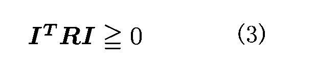
任意の実ベクトルIに対して式(4)が成立するため、行列Rは半正定値である。つまり、導体メッシュにおける効率を最大化するループコイルの電流分布はMISOシステムにおける効率最大化問題と同様に解を得ることができる。
4. 電流分布導出の例
初期検討として、100x100の導体メッシュを想定し、各ループを構成する1辺の抵抗値をr、各ループと受電共振器間の相互インダクタンスがMで一定という条件の下で電流分布を導出する。ここで相互インダクタンスが一定であるということは、受電共振器が生じる磁界分布が均一であるということを意味している。
初期検討として、100x100の導体メッシュを想定し、各ループを構成する1辺の抵抗値をr、各ループと受電共振器間の相互インダクタンスがMで一定という条件の下で電流分布を導出する。ここで相互インダクタンスが一定であるということは、受電共振器が生じる磁界分布が均一であるということを意味している。
図8は、導出した電流分布の一例を示す図である。ここで横方向については正(負)の値は右(左)向きを表し、縦方向の正(負)の値は上(下)方向を表している。
5. 磁気双極子モーメントによるアンテナコイルの形状の導出
図8に示されるような電流分布を再現するアンテナコイルの形状の導出について説明する。各電流ループの導出された電流分布は各ループ間で離散的な値をとるため、与えられた電流分布を一つのコイルによって直接再現することは困難である。そこで、磁界共振結合型の基本原理が電磁誘導型と同様、電流が生み出す磁界を介している点に注目し、各ループが生み出す磁界を再現するように共振器を設計する。
図8に示されるような電流分布を再現するアンテナコイルの形状の導出について説明する。各電流ループの導出された電流分布は各ループ間で離散的な値をとるため、与えられた電流分布を一つのコイルによって直接再現することは困難である。そこで、磁界共振結合型の基本原理が電磁誘導型と同様、電流が生み出す磁界を介している点に注目し、各ループが生み出す磁界を再現するように共振器を設計する。
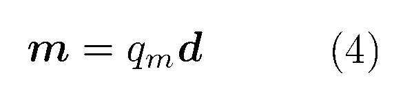
位置rにおける磁界は、磁気双極子モーメントを用いて表現することが可能である。磁気双極子モーメントmとは、磁荷の大きさがqmで等しい正負の磁極対を仮定し、負の磁荷から正の磁荷を向き、磁極間の距離dの大きさを持つベクトルdを用いて、式(4)として定義される。
磁界B(r)は磁気双極子モーメントを用いて式(5)で表される。

実際には、単独で存在する磁極は見出されておらず、磁気双極子モーメントmは、位置rでの電流密度Je(r)によって式(6)で定義され、式(4)と同値である。

ここで、r’は原点から電流が存在する領域までの位置ベクトル、Vは、電流が分布する領域である。以上から、導体メッシュの各ループが生み出す磁気双極子モーメント求め、再現することで電流分布による磁界を生み出すことができる。電流ループによって囲まれる領域の磁気双極子モーメントは式(6)によって定義されたが、それぞれの磁気双極子モーメントを再現するため、ループをさらに微小なループに分割した際の各微小領域の持つ磁気双極子モーメントについて考える。
図9は、微小領域の磁気双極子モーメントを説明する図である。導電電流Iが流れる閉ループCを囲まれた面を面積ΔSiの無数の微小面積に分割し、全ての微小ループに同じ電流Iを仮想的に流したとする。各微小ループは、モーメントmi=μ0IΔSiを持つ磁気双極子に置き換えることができる。
微小ループの隣り合う電流は互いに打ち消しあって、全体としては閉ループCに流れる電流だけが残り、各微小ループの持つ磁気双極子モーメントの和は元々のループCにおける磁気双極子モーメントと一致する。
つまり、同じ大きさの磁気双極子モーメントを持つループは、それらを囲ったひとつのループに適当な電流を流すことで、まとめて再現することが可能であり、その際の電流は、領域の面積と各ループの磁気双極子モーメントの大きさの関係から、式(7)と求めることができる。

ここで、Siはループが囲う領域の面積、miは囲まれた領域内のループが生み出す磁気双極子モーメントの大きさ、μ0は真空の透磁率を表す。
図10は、図8の電流分布から導出される磁気双極子モーメントの分布の一例を示す図である。
6. アンテナコイルの形状の導出
本実施の形態では、磁気双極子モーメントの分布の等高線を利用することで、共振器の外形を提示する。なお、等高線は|mmax|/n巻数ごとに引く。mmaxは、磁気双極子モーメントの最大値である。
本実施の形態では、磁気双極子モーメントの分布の等高線を利用することで、共振器の外形を提示する。なお、等高線は|mmax|/n巻数ごとに引く。mmaxは、磁気双極子モーメントの最大値である。
図11(a)、(b)は、図10の磁気双極子モーメントの分布から得られるアンテナコイルの形状の一例を示す図である。ここでは100x100の導体メッシュの電流分布について、磁気双極子モーメントの等高線を用いて、アンテナコイルの概形決定を行っており、コイルの巻数は5としている。図10(a)に示すように、アンテナコイルの形状は、等高線に沿うように規定すればよいが、すべてのアンテナコイルに流れる電流が同一であることを前提としているから、最終的にアンテナコイルは、図10(b)に示すように、1本の導体として設計することができる。
7. 伝送効率の検証
本設計方法により導出されたアンテナコイルの形状と、一般的に効率が高いとされるコイル形状の伝送効率について比較する。ここではkQ積によって伝送効率を比較する。
本設計方法により導出されたアンテナコイルの形状と、一般的に効率が高いとされるコイル形状の伝送効率について比較する。ここではkQ積によって伝送効率を比較する。
送電装置10と受電装置20の等価回路からkQ積を求め、kQ積によって効率の改善を確認する。図12(a)、(b)は、複数の送信側共振器を備える無線給電システム2の等価回路図である。kQ積を求める際、図12(b)に示されるように、送信側の多数の共振器を一つの共振器としてまとめる。各微小ループでの、電流の比率をSi=Ii/Imaxとして定義すると、一つにまとめた際の抵抗成分rtotalは共振器アレイによって生じる損失成分に基づいて、式(8)で表される。

ここで、iとjは辺を共有するループである。受電側のコイルに生じる電圧は、共振器の共振角周波数ωを用いて式(9)となるから、Mtotal=MΣiSiと定義できる。
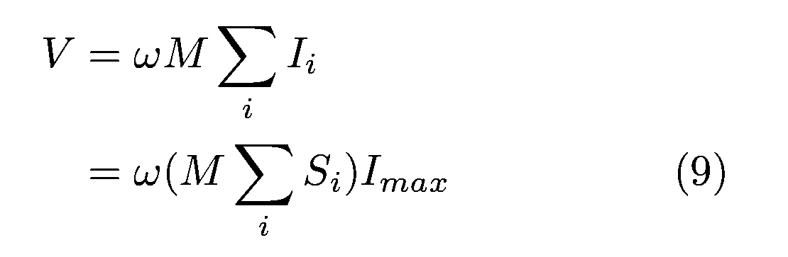
その結果、一つにまとめられた送電側の共振器と受電側の共振器のkQ積は式(10)となる。

本手法の有用性を確認するため、一般に効率が高いとされる外側に巻線を集中させたアンテナコイルと本手法によって提示されたアンテナコイルについて比較を行った。巻数を5に固定し、導体メッシュの数を10x10,50x50,100x100と変化させた場合のkQ積の比をとった結果、それぞれ1.24,1.93,3.30となり、いずれのメッシュ数においても、本設計方法による共振器の方がkQ積が高くなった。また、メッシュ数を増やすほど、kQ積の改善量は大きくなることがわかる。
また、メッシュ数を100x100に固定し、巻き数を3,5,7と変化させた場合においても、それぞれ5.18,3.30,2.51となり本設計方法による共振器の方がkQ積が高くなり、効率の改善を確認できた。
8. 分散リアクタンス補償
アンテナの物理形状は周波数により制限される。この認識は放射型のアンテナのみならず、磁界共振結合型無線電力伝送で用いる共振器に対しても同様である。動作周波数が高く、また、共振器形状が大きくなると、電流分布に偏りが生じ、ときには共振器内部で電流の向きが逆転する。その際、共振器内で磁界が相殺されることにより、共振器の性能指標であるQ値の低下に直結する。
アンテナの物理形状は周波数により制限される。この認識は放射型のアンテナのみならず、磁界共振結合型無線電力伝送で用いる共振器に対しても同様である。動作周波数が高く、また、共振器形状が大きくなると、電流分布に偏りが生じ、ときには共振器内部で電流の向きが逆転する。その際、共振器内で磁界が相殺されることにより、共振器の性能指標であるQ値の低下に直結する。
共振器設計のパラメータ調整がいまだ試行錯誤的に行われている一因も電流分布の不均一性にある。本設計方法においても、1本の導体(アンテナコイル)に流れる電流は、均一であることを前提としたものである。ゆえに、適用できる共振器形状は電気的に小型とみなせる範囲に制限される可能性がある。もし、電流分布の不均一性を改善できれば、本設計方法の適用範囲は格段に拡大される。
電流分布の不均一性は、アンテナコイルである導線を一種の伝送線路とした際に、線路間に存在する寄生キャパシタに電荷が蓄えられることに起因する。図13(a)、(b)は、損失ありおよび無損失の伝送回路の等価回路図である。単位長あたりのインダクタンスをL、単位長あたりの容量をC、LとCに付随した損失成分をそれぞれRとGとする。RとGが十分小さいとみなせる場合には、図13(b)に示すように、無損失線路となる。
本発明者らは、分散リアクタンス補償(DRC:Distributed Reacquantance Compensation)について提案している(非特許文献3)。この分散リアクタンス補償は、もともと、入力ポートだけでなくアンテナコイル中にリアクタンス補償のキャパシタを挿入することで、アンテナコイル周辺の磁界強度を弱め、誘電体損失を低減する技術として提案したものである。
従来の集中リアクタンス補償(CRC: Concentrated ReacquantanceCompensation)とは異なり、分散リアクタンス補償では、アンテナコイル内に多数のキャパシタンスを挿入することで、コイル内で共振状態を実現し、線路間での電圧差を低減させ、寄生キャパシタに蓄えられる電荷が減少させている。
本発明者らは、分散リアクタンス補償により、誘電体損失の低減のみでなく、アンテナコイルの電流分布の均一化される現象を見いだした。なおこの現象を公知技術とみなしてはならない。
図14は、分散リアクタンス補償を説明する等価回路図である。アンテナコイルは、複数の要素に分割され、それらの間に補償用のキャパシタが挿入されている。
図15(a)~(d)は、分散リアクタンス補償による電流分布のシミュレーション結果を示す図である。動作周波数6.78MHzにおける直径5mのループコイルの電流分布を電磁界シミュレーションにより計算した。ループコイルの線径は1mm、材質は銅とし、シミュレータにはAltair inc.社製のFEKOを用いた。
図15(a)は、補償無しの場合を示す。分散リアクタンス補償は施さず、リアクタンス補償用のキャパシタは入力ポートに接続する。電流分布は共振器内における最大値で正規化している。入力ポート部分で電流強度は最小となり、ポートから最も離れた部分と比較すると約30%程度の電流強度に留まっている。この結果は、動作周波数6.78MHzにおいて、巻数1のアンテナであっても電流分布が大きく歪みうることを示しており、電流分布の歪みは巻数が増えるに従ってさらに増大する。
図15(b)~(d)は、分散リアクタンス補償を施した場合のシミュレーション結果を示す。分散リアクタンス補償に用いるキャパシタの数Nは2,4,8の3通りである。電流分布が均一であるとき、各キャパシタにおける電流と入力ポートを流れる電流とは、その強度および向きが等しくなる。この条件に基づき、電流分布が均一となるキャパシタンスを考える。
キャパシタンスの導出には、キャパシタを接続する箇所をポートとして電磁界シミュレーションを行い、N+1ポートの回路網として導出したSパラメータを使用する。Sパラメータを変換して得られるZパラメータを用いると、各ポートの電流が等しくIとなる条件は、-ZcI=Z’(1,1,1,…,1)TIにより記述できる。ここで、Z’はインピーダンス行列Zから入力ポートに該当する行を削除したN×(N+1)行列、Zcは接続するキャパシタのインピーダンスから成るN次の行ベクトルである。接続すべきキャパシタンスは式(11)を解くことによって求められる。
Zc=-Z’(1,1,1,…,1)T (11)
Zc=-Z’(1,1,1,…,1)T (11)
直径5mのループコイルに等間隔でキャパシタを配置し、式(11)によりキャパシタンスを計算したところ、対称性により値は位置に依存せず、N=2のとき56.7pF、N=4のとき98.1pF、N=8のとき179.4pFとなった。
図15(b)~(d)においては、電流分布をより詳細に示すため、各図により、濃淡と電流値との対応が異なることに注意されたい。入力ポートおよびキャパシタ挿入部分における電流分布が等しくなっており、また、分散リアクタンス補償に用いるキャパシタの個数が増えるほどに電流分布が均一になることを確認できる。N=8のとき、共振器内における電流強度の差異は1%以下に抑えられる。
分散リアクタンス補償によって電流分布が均一になる要因は伝送線路理論により考察できる。共振器内の導線を一種の伝送線路としてみたとき、電流分布が不均一となるのは、線路間に存在する寄生キャパシタに電荷が蓄えられることによる。分散リアクタンス補償は共振器内に多数のキャパシタンスを配置することで線路間の電位差を低減させるため、寄生キャパシタに蓄えられる電荷が減少し、電流分布が均一化したものと考えられる。
このように、分散リアクタンス補償を行うことで、アンテナコイルの電流分布が均一化できる。そこで本設計方法を利用したソフトウェアプログラムには、数MHzあるいはそれ以上の周波数帯域で使用されるアンテナ設計に際しては、分散リアクタンス補償を組み込むことが好ましい。
上述の本設計手法により、アンテナコイルの形状が決定される。そして、アンテナコイルに対して分散補償に関する追加の処理が実行される。挿入すべきキャパシタの個数Nは、マニュアルで指定してもよいし、図15(a)に示すように補償無しのときの電流の不均一性を計算し、不均一性にもとづいて、キャパシタの個数Nを決定してもよい。
そして、アンテナコイルの形状が既知であれば、それを伝送線路とみなしたときのSパラメータ(Zパラメータ)が計算できる。Nが定まると、Zパラメータを利用して、式(11)を解くことにより、挿入すべきキャパシタの容量値を計算することができる。
実施の形態にもとづき、具体的な用語を用いて本発明を説明したが、実施の形態は、本発明の原理、応用を示しているにすぎず、実施の形態には、請求の範囲に規定された本発明の思想を逸脱しない範囲において、多くの変形例や配置の変更が認められる。
本発明は、無線給電に利用できる。
2 無線給電システム
10 送電装置
20 受電装置
LTX 送電コイル
CTX 共振キャパシタ
LRX 受電コイル
CRX 共振キャパシタ
10 送電装置
20 受電装置
LTX 送電コイル
CTX 共振キャパシタ
LRX 受電コイル
CRX 共振キャパシタ
Claims (8)
- アンテナコイルの設計方法であって、
対を成すアンテナコイルを含む周囲環境をモデル化するステップと、
設計対象のアンテナを配置すべき空間を複数のメッシュに区切り、前記モデル化された前記周辺環境における各メッシュの最適な電流量を計算するステップと、
前記複数のメッシュの電流分布から前記設計対象のアンテナコイルの形状を取得するステップと、
を備えることを特徴とするアンテナコイルの設計方法。 - 前記複数のメッシュの電流分布から、磁気双極子モーメントの分布を計算するステップと、
前記磁気双極子モーメントの分布の等高線を取得するステップと、
をさらに備え、前記設計対象のアンテナコイルの形状は、前記等高線に応じていることを特徴とする請求項1に記載の設計方法。 - アンテナコイルの設計方法であって、
対を成すアンテナコイルを含む周囲環境をモデル化するステップと、
設計対象のアンテナを配置すべき空間を複数のメッシュに区切り、前記モデル化された前記周辺環境における各メッシュの最適な磁気双極子モーメントを計算するステップと、
前記複数のメッシュの磁気双極子モーメントの分布の等高線を取得するステップと、
前記等高線にもとづいて前記アンテナコイルの形状を取得するステップと、
を備えることを特徴とするアンテナコイルの設計方法。 - 前記設計対象のアンテナを複数の要素に分割し、分割された要素の間に、キャパシタを挿入するステップをさらに備えることを特徴とする請求項1から3のいずれかに記載のアンテナコイルの設計方法。
- コンピュータに、
対を成すアンテナコイルを含む周囲環境をモデル化させるステップと、
設計対象のアンテナを配置すべき空間を複数のメッシュに区切り、前記モデル化された前記周辺環境における各メッシュの最適な電流量を計算させるステップと、
前記複数のメッシュの電流分布からアンテナコイルの形状を取得させるステップと、
を実行させるためのプログラム。 - 前記コンピュータに、
前記複数のメッシュの電流分布から、磁気双極子モーメントの分布を計算するステップと、
前記磁気双極子モーメントの分布の等高線を取得するステップと、
前記等高線に応じて前記設計対象のアンテナコイルの形状を取得するステップと、
をさらに実行させることを特徴とする請求項5に記載のプログラム。 - コンピュータに、
対を成すアンテナコイルを含む周囲環境をモデル化するステップと、
設計対象のアンテナを配置すべき空間を複数のメッシュに区切り、前記モデル化された前記周辺環境における各メッシュの最適な磁気双極子モーメントを計算するステップと、
前記複数のメッシュの磁気双極子モーメントの分布の等高線を取得するステップと、
前記等高線にもとづいて前記設計対象のアンテナコイルの形状を取得するステップと、
を実行させることを特徴とするプログラム。 - コンピュータに、
前記設計対象のアンテナを複数の要素に分割し、分割された要素の間に、キャパシタを挿入するステップをさらに実行させることを特徴とする請求項5から7のいずれかに記載のプログラム。
Applications Claiming Priority (2)
| Application Number | Priority Date | Filing Date | Title |
|---|---|---|---|
| JP2018158726A JP7236717B2 (ja) | 2018-08-27 | 2018-08-27 | アンテナコイルの設計方法およびそのプログラム |
| JP2018-158726 | 2018-08-27 |
Publications (1)
| Publication Number | Publication Date |
|---|---|
| WO2020045273A1 true WO2020045273A1 (ja) | 2020-03-05 |
Family
ID=69643275
Family Applications (1)
| Application Number | Title | Priority Date | Filing Date |
|---|---|---|---|
| PCT/JP2019/033009 Ceased WO2020045273A1 (ja) | 2018-08-27 | 2019-08-23 | アンテナコイルの設計方法およびそのプログラム |
Country Status (2)
| Country | Link |
|---|---|
| JP (1) | JP7236717B2 (ja) |
| WO (1) | WO2020045273A1 (ja) |
Cited By (3)
| Publication number | Priority date | Publication date | Assignee | Title |
|---|---|---|---|---|
| CN115828647A (zh) * | 2023-02-22 | 2023-03-21 | 广东电网有限责任公司湛江供电局 | 一种无线供电系统线圈模型确定方法、系统、设备和介质 |
| CN121145777A (zh) * | 2025-09-16 | 2025-12-16 | 中国石油集团长城钻探工程有限公司 | 片上线圈天线、天线集总参数模型构建方法和装置 |
| CN121145777B (zh) * | 2025-09-16 | 2026-05-19 | 中国石油集团长城钻探工程有限公司 | 片上线圈天线、天线集总参数模型构建方法和装置 |
-
2018
- 2018-08-27 JP JP2018158726A patent/JP7236717B2/ja active Active
-
2019
- 2019-08-23 WO PCT/JP2019/033009 patent/WO2020045273A1/ja not_active Ceased
Non-Patent Citations (1)
| Title |
|---|
| SASATANI, TAKUYA ET AL.: "Genetic Algorithm-Based Design of Recieving Resonator Arrays for Wireless Power Transfer via Magnetic Resonant Coupling", PROCEEDINGS OF THE 2016 IEEE WIRELESS POWER TRANSFER CONFERENCE, 5 May 2016 (2016-05-05), pages 1 - 4, XP032916228, DOI: 10.1109/WPT.2016.7498842 * |
Cited By (3)
| Publication number | Priority date | Publication date | Assignee | Title |
|---|---|---|---|---|
| CN115828647A (zh) * | 2023-02-22 | 2023-03-21 | 广东电网有限责任公司湛江供电局 | 一种无线供电系统线圈模型确定方法、系统、设备和介质 |
| CN121145777A (zh) * | 2025-09-16 | 2025-12-16 | 中国石油集团长城钻探工程有限公司 | 片上线圈天线、天线集总参数模型构建方法和装置 |
| CN121145777B (zh) * | 2025-09-16 | 2026-05-19 | 中国石油集团长城钻探工程有限公司 | 片上线圈天线、天线集总参数模型构建方法和装置 |
Also Published As
| Publication number | Publication date |
|---|---|
| JP2020035028A (ja) | 2020-03-05 |
| JP7236717B2 (ja) | 2023-03-10 |
Similar Documents
| Publication | Publication Date | Title |
|---|---|---|
| Jonah et al. | Wireless power transfer in concrete via strongly coupled magnetic resonance | |
| CN107453790B (zh) | 无线天线结构 | |
| Ahn et al. | Enhanced wireless power transmission using strong paramagnetic response | |
| KR101584800B1 (ko) | 다중 모바일 기기들의 무선 충전을 위한 자기공진방식 무선전력전송 안테나 | |
| Lim et al. | Reconfigurable coil array for near-field beamforming to compensate for misalignment in WPT systems | |
| Hirayama | Equivalent circuit and calculation of its parameters of magnetic-coupled-resonant wireless power transfer | |
| Hirayama et al. | A consideration of electro-magnetic-resonant coupling mode in wireless power transmission | |
| Mirbozorgi et al. | Multi‐resonator arrays for smart wireless power distribution: comparison with experimental assessment | |
| Tan et al. | Output power stabilisation of wireless power transfer system with multiple transmitters | |
| Wang et al. | Optimisation analysis of coil configuration and circuit model for asymmetric wireless power transfer system | |
| US10291067B2 (en) | Computer modeling for resonant power transfer systems | |
| Honjo et al. | Suppressing leakage magnetic field in wireless power transfer using Halbach array-based resonators | |
| Poon | A general solution to wireless power transfer between two circular loop | |
| CN110912283B (zh) | 一种无线电能传输系统的参数调整方法及装置 | |
| Chen et al. | Metamaterial for wireless power transfer system at 13.56 MHz with coil misalignment | |
| Lee et al. | Effect of quality factor on determining the optimal position of a transmitter in wireless power transfer using a relay | |
| JP7236717B2 (ja) | アンテナコイルの設計方法およびそのプログラム | |
| Huang et al. | A spiral electrically small magnetic antenna with high radiation efficiency for wireless power transfer | |
| Rong et al. | A novel coil array compensation structure design with high-misalignment tolerance for UAV-enable WPT system | |
| CN102769341B (zh) | 一种用非共振磁耦合线圈阵列构建无线供电装置的方法 | |
| Lee et al. | Simultaneous information and power transfer using magnetic resonance | |
| Ali et al. | Analysis of symmetric two and four-coil magnetic resonant coupling wireless power transfer | |
| Nguyen et al. | Magnetic resonance wireless power transfer for laptop computer with a ground plane | |
| Mishra et al. | Development of WiTricity based wireless power transmission system | |
| Moshfegh et al. | Conditions of maximum efficiency for wireless power transfer between two helical wires |
Legal Events
| Date | Code | Title | Description |
|---|---|---|---|
| NENP | Non-entry into the national phase |
Ref country code: DE |
|
| 122 | Ep: pct application non-entry in european phase |
Ref document number: 19854215 Country of ref document: EP Kind code of ref document: A1 |