WO2020032352A1 - 유전체 장벽 방전 시스템 - Google Patents
유전체 장벽 방전 시스템 Download PDFInfo
- Publication number
- WO2020032352A1 WO2020032352A1 PCT/KR2019/005871 KR2019005871W WO2020032352A1 WO 2020032352 A1 WO2020032352 A1 WO 2020032352A1 KR 2019005871 W KR2019005871 W KR 2019005871W WO 2020032352 A1 WO2020032352 A1 WO 2020032352A1
- Authority
- WO
- WIPO (PCT)
- Prior art keywords
- pattern
- barrier discharge
- dielectric barrier
- discharge system
- plasma
- Prior art date
- Legal status (The legal status is an assumption and is not a legal conclusion. Google has not performed a legal analysis and makes no representation as to the accuracy of the status listed.)
- Ceased
Links
Images



Classifications
-
- H—ELECTRICITY
- H05—ELECTRIC TECHNIQUES NOT OTHERWISE PROVIDED FOR
- H05H—PLASMA TECHNIQUE; PRODUCTION OF ACCELERATED ELECTRICALLY-CHARGED PARTICLES OR OF NEUTRONS; PRODUCTION OR ACCELERATION OF NEUTRAL MOLECULAR OR ATOMIC BEAMS
- H05H1/00—Generating plasma; Handling plasma
- H05H1/24—Generating plasma
- H05H1/2406—Generating plasma using dielectric barrier discharges, i.e. with a dielectric interposed between the electrodes
- H05H1/2437—Multilayer systems
-
- H—ELECTRICITY
- H05—ELECTRIC TECHNIQUES NOT OTHERWISE PROVIDED FOR
- H05H—PLASMA TECHNIQUE; PRODUCTION OF ACCELERATED ELECTRICALLY-CHARGED PARTICLES OR OF NEUTRONS; PRODUCTION OR ACCELERATION OF NEUTRAL MOLECULAR OR ATOMIC BEAMS
- H05H1/00—Generating plasma; Handling plasma
- H05H1/24—Generating plasma
-
- H—ELECTRICITY
- H05—ELECTRIC TECHNIQUES NOT OTHERWISE PROVIDED FOR
- H05H—PLASMA TECHNIQUE; PRODUCTION OF ACCELERATED ELECTRICALLY-CHARGED PARTICLES OR OF NEUTRONS; PRODUCTION OR ACCELERATION OF NEUTRAL MOLECULAR OR ATOMIC BEAMS
- H05H2277/00—Applications of particle accelerators
- H05H2277/10—Medical devices
Definitions
- the present invention relates to a dielectric barrier discharge plasma, and more particularly to a dielectric barrier discharge system.
- DBD Dielectric Barrier Discharge
- the dielectric barrier discharge system consists of two parallel metal electrodes, at least one of which is covered with a dielectric layer.
- Atomic layer deposition (ALD), E-beam evaporation, sputter, lithography techniques can be used to fabricate the electrodes of the dielectric barrier discharge system.
- the electrode may be manufactured by bending or cutting a metal wire and a metal film.
- Atomic layer deposition, electron beam deposition, sputtering, lithography and the like have advantages in that fine electrode manufacturing is possible, but requires expensive equipment and has problems in that electrode formation speed is slow. And when using a metal wire and a metal film, although a manufacturing method is simple and an electrode can be manufactured easily, there exists a problem that manufacture of a fine electrode structure is difficult. As a result, there is a need for a new pattern electrode manufacturing technology that can solve these problems.
- An object of the present invention is to provide a dielectric barrier discharge system in which the dielectric barrier discharge plasma discharge intensity is controlled and the plasma discharge intensity is excellent even when a lower voltage is applied.
- Dielectric barrier discharge system for one object of the present invention comprises a dielectric layer formed on the second electrode; A pattern seed layer formed on the dielectric layer and having a pattern; And a pattern metal layer formed on the pattern seed layer and having a pattern.
- An exemplary pattern of the patterned metal layer in the example may be a contour length (Contour length) / area (Area) ratios (C / A) is 1.3cm -1 to 500cm -1.
- the pattern metal layer may be formed in a zigzag pattern.
- the thickness of the pattern seed layer may be 1 nm to 10 nm.
- the dielectric barrier discharge system can be used in small plasma apparatus and plasma medicine applications.
- the dielectric barrier discharge system of the present invention is more economical, more productive, and has a higher profile contour length due to lower process costs than the prior art, so that plasma discharge intensity can be increased even when a relatively low voltage is applied.
- the dielectric barrier discharge system of the present invention may be applicable to various fields such as plasma medicine, plasma actuator, and micro reactor.
- FIG. 1 is a schematic diagram illustrating a part of a method of manufacturing a dielectric barrier discharge system according to an embodiment of the present invention.
- FIG. 2 illustrates a seed layer pattern according to an embodiment of the present invention.
- FIG 3 is a view showing the surface of the patterned metal layer by the electroless plating time according to an embodiment of the present invention.
- FIG. 4 is a schematic diagram of a dielectric barrier discharge system in accordance with an embodiment of the present invention.
- 5 to 7 are diagrams showing plasma characteristics of a dielectric barrier discharge system according to an embodiment of the present invention.
- FIG. 8 is a diagram illustrating an electrode pattern manufactured according to an exemplary embodiment.
- 9 and 10 are views showing the effect of the electrode shape according to an embodiment of the present invention.
- the present invention relates to a dielectric barrier discharge (DBD) system with increased discharge intensity of a plasma.
- DBD dielectric barrier discharge
- Stronger electric fields are formed at the edges of the electrodes, and the dielectric barrier discharge system of the present invention increases the contour length of the electrodes by forming patterns on the electrodes included in the system, thereby increasing the relative length of the electrodes. Even if a low voltage is applied, a higher intensity plasma can be obtained.
- the dielectric barrier discharge system of the present invention can control the plasma intensity by adjusting the pattern shape of the electrode.
- the dielectric barrier discharge system of the present invention comprises a dielectric layer formed on a second electrode; A pattern seed layer formed on the dielectric layer and having a pattern; And a pattern metal layer formed on the pattern seed layer and having a pattern.
- the dielectric barrier discharge system may include a structure in which the second electrode, the dielectric layer, the pattern seed layer, and the pattern metal layer are sequentially stacked.
- the pattern metal layer means a first electrode having a pattern.
- the second electrode may include the same metal as the pattern metal layer, and may include different metals.
- the pattern metal layer may include copper
- the second electrode may include iron
- the second electrode may be a wire mesh.
- the dielectric layer may include a material having a high dielectric constant
- the pattern seed layer and the pattern metal layer may include a metal
- the dielectric layer may include quartz, glass, alumina (aluminum oxide), titania (titanium oxide), zirconia (zirconium oxide), zinc oxide, iron oxide, carbon nanotubes, and the metal may be gold, silver, platinum, or the like. , Copper, aluminum, tungsten and alloys thereof.
- the pattern seed layer and the pattern metal layer may include the same metal, and may include different metals.
- the pattern seed layer may include gold
- the pattern metal layer may include copper.
- the pattern seed layer may be formed using platinum or palladium.
- platinum or palladium has a disadvantage in that a seed layer is formed from a solution containing fluorine, and thus a high risk is used and a high cost of materials is used.
- the pattern seed layer is formed using gold by sputtering, the process may be relatively more expensive than using platinum or palladium and may be manufactured at a relatively low cost.
- the pattern layer may be formed of a metal having high conductivity, such as copper, gold, silver, or platinum, but in the case of forming the pattern metal layer using copper, there is an advantage in that the conductivity is high and the manufacturing cost is low. .
- An exemplary pattern of the patterned metal layer in the example may be a contour length (Contour length) / area (Area) ratios (C / A) is 1.3cm -1 to 500cm -1.
- the contour length / area ratio of the pattern may be a 6.5cm -1 to 500cm -1.
- the pattern of the pattern metal layer is not limited thereto, and may be formed in various patterns such as a square, dumbbell, saw, star, and zigzag patterns. Can be.
- the pattern metal layer may be a zigzag pattern.
- the thickness of the pattern metal layer may be 100 nm to 50 ⁇ m.
- the thickness of the pattern seed layer may be 1 nm to 10 nm.
- the thickness of the pattern seed layer may be 1 nm to 10 nm.
- the pattern seed layer may be difficult to be stably maintained, the pattern metal layer may be difficult to be stacked on the pattern seed layer, and the pattern seed layer may be If the thickness is greater than 10nm may cause a variety of problems in the manufacturing process, there may occur a problem that the effect of increasing the plasma intensity is relatively small.
- the method of manufacturing a pattern electrode structure included in the dielectric barrier discharge system of the present invention includes a first step of forming a pattern seed layer on a dielectric layer; And a second step of forming a pattern metal layer on the pattern seed layer through electroless plating.
- the first step may be a step of forming a seed layer on the surface of the dielectric thin film or the dielectric layer.
- the seed layer may be the pattern seed layer having a predetermined pattern.
- the dielectric may be a ceramic, a polymer having a high dielectric constant, and may be used without limitation.
- the first step may be to form the pattern seed layer on the dielectric surface through sputtering.
- the pattern seed layer may be formed on a dielectric layer to form the pattern seed layer, and then the seed layer material is deposited to form the pattern seed layer.
- the seed layer material may be deposited only in the open space of the pattern mask through sputtering.
- the seed layer material may be used as gold, silver, platinum, copper, zinc, nickel, cobalt, phosphorus, manganese, and the like, but is not limited thereto, and various materials capable of serving as seed layers of electroless plating may be used. Can be.
- the pattern mask may be simply manufactured using a 3D printer.
- the pattern size of the pattern seed layer may be variously adjusted according to the size and shape of the pattern mask, and the pattern mask may be removed after the sputtering process and may be reused.
- the thickness of the seed layer may be adjusted by adjusting the time and / or current amount of sputtering.
- the sputtering conditions may be adjusted such that the thickness of the pattern seed layer is 1 nm to 10 nm.
- the second step may be to form the pattern metal layer by depositing a metal on the pattern seed layer through electroless plating.
- an electroless plating bath may be prepared for the electroless plating, and may be used without limiting the material used for the electroless plating.
- a material comprising copper may be used to produce a copper electroless plating bath.
- the electroless plating of the second step may be an electroless plating using a material containing copper.
- the plating temperature for the electroless plating may be 50 ° C to 90 ° C.
- the plating temperature may be 70 °C.
- a plating rate may be lowered, and at a temperature above 75 ° C., a plating solution may evaporate.
- the pH range of the electroless plating bath may be 11 to 13.
- the electroless plating bath may be pH 12. If the pH is 11 or less, a problem that the plating rate is significantly reduced may occur.
- the electroless plating process time may be performed for 0.1 to 30 minutes.
- FIG. 1 is a schematic diagram illustrating a part of a method of manufacturing a dielectric barrier discharge system according to an embodiment of the present invention.
- a pattern seed layer is formed on the surface of the dielectric through sputtering, and then a copper electroless plating bath is manufactured, and the copper electroless plating bath is manufactured.
- a copper thin film on the pattern seed layer is formed on the pattern seed layer to form a pattern electrode structure usable for a dielectric barrier discharge system.
- FIG. 2 illustrates a pattern of a pattern seed layer according to an exemplary embodiment of the present invention.
- a pattern seed layer having various patterns may be formed through the pattern mask, and an example of a pattern that may be formed is illustrated in FIG. 2.
- the pattern of the pattern seed layer may be rectangular, dumbbell, saw, star, zigzag, or the like.
- An electroless plating bath was prepared according to an embodiment of the present invention. Copper electroless plating baths were treated with CuSO 4 ⁇ 5H 2 O (9 g / L), HCHO (8.5 g / L), Ethylenediaminetetraacetic acid tetrasodium salt hydrate (35 g / L) in secondary distilled water. It was prepared by dissolving. The pH of the plating bath was adjusted to 12 using 1 M NaOH solution at room temperature.
- a pattern electrode structure for a dielectric barrier discharge system was manufactured. At this time, a zirconia plate was used as the dielectric.
- a pattern mask was formed by placing a pattern mask on the zirconia plate surface, and then depositing a gold seed layer on the zirconia plate surface by applying 4 mA for 20 seconds in an ion sputter device.
- the copper electroless plating bath prepared according to one embodiment of the present invention was used, the stirring speed was 150rpm, the plating temperature was adjusted to 70 °C.
- the zirconia plate in which the seed layer was formed was immersed in the copper electroless plating bath, taken out after a predetermined time, and washed and dried. Regardless of the pattern shape, the area of the copper thin film was about 9.5 cm 2, which was similar to minimize the effect of the area on the plasma intensity.
- the pattern metal layer is formed on the pattern seed layer, for example, a copper thin film is plated on a gold pattern seed layer having a pattern. Appeared the same.
- FIG. 3 is a view showing the surface of the patterned metal layer by the electroless plating according to an embodiment of the present invention.
- FIG. 3 illustrates an electroless plating pattern metal layer of a pattern electrode structure in which a dielectric layer is a zirconia plate, a pattern seed layer is a gold seed layer, and a pattern metal layer is a copper thin film, that is, electroless plating is performed according to time. The surface change of the thin film is shown.
- electroless plating was performed for about 5 minutes, a uniform copper thin film was formed on the surface of the zirconia plate, and a pattern was formed on the entire surface to a thickness of about 8 ⁇ m.
- the dielectric barrier discharge system of the present invention was manufactured by using the pattern electrode structure manufactured according to the above embodiment.
- 4 is a schematic view of a dielectric barrier discharge system according to an embodiment of the present invention.
- the dielectric barrier discharge system illustrated in FIG. 4A includes a pattern electrode structure manufactured according to an embodiment of the present invention, and specifically includes a substrate, a pattern metal layer, a dielectric layer, and a second electrode.
- the pattern metal layer represents a pattern metal layer of the pattern electrode structure of the present invention
- the pattern metal layer and the dielectric layer of FIG. 4A are examples of the pattern electrode structure of the present invention.
- the 4B includes a pattern electrode structure manufactured according to an embodiment of the present invention, specifically, a Teflon substrate, a copper thin film having a pattern with the pattern metal layer, and a zirconia plate with a dielectric layer.
- the patterned electrode structure including, and the wire mesh (SUS mesh) as a second electrode, each thickness is shown in FIG.
- an AC power of 25 kHz frequency was applied at 15 kV to the dielectric barrier discharge system manufactured according to one embodiment.
- the discharge gas was discharged using air without using any other gas.
- the temperature was kept constant at 25 degreeC.
- OES optical emission spectroscopy
- FIG. 5 to 7 are diagrams illustrating dielectric barrier discharge plasma characteristics according to an embodiment of the present invention, wherein the same voltage is applied to dielectric barrier discharge systems fabricated using various pattern electrode structures. The results of the analysis are shown.
- FIG. 5 is a diagram illustrating dielectric barrier discharge plasma characteristics according to an embodiment of the present invention
- FIG. 5 (a) shows an OES spectrum result of the dielectric barrier discharge plasma according to the shape of the pattern electrode structure.
- b) shows the contour length and plasma intensity of each pattern.
- the peak intensity of the OES spectrum increased as the contour length of the pattern increased, and the plasma intensity increased as the contour length increased.
- the peak intensity of the OES spectrum was similar in the case of the saw and star patterns having different patterns but having the same area and contour length. Therefore, it can be seen that the plasma intensity is influenced by the contour length rather than the shape of the pattern.
- FIG. 6 illustrates the concentration of gas generated in the plasma according to the contour length of the pattern electrode structure according to the exemplary embodiment of the present invention. It can be seen that when the contour length of the pattern of the pattern electrode structure increases, the concentration of ozone (O 3 ) and nitrogen dioxide (NO 2 ) increases. If the plasma discharge intensity is increased, the concentration of chemical species in the plasma may be increased, thereby increasing the reaction rate for generating gas. Therefore, increasing the contour length of the pattern electrode structure improves the plasma intensity, thereby increasing the concentration of the reaction gas generated.
- O 3 ozone
- NO 2 nitrogen dioxide
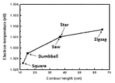
- FIG. 7 shows a change in electron temperature according to the contour length of the pattern electrode structure according to the exemplary embodiment of the present invention. It can be seen that the electron temperature increases as the contour length of the pattern electrode structure increases. The higher the strength of the electric field, the higher the electron temperature, since the electron can accumulate more energy. Referring to FIG. 7, it can be seen that the electron temperature increases as the contour length increases, so that the strength of the electric field increases as the contour length increases. As a result, even when the same voltage is applied through the present invention, when the contour length of the pattern electrode structure is increased, it can be seen that the plasma intensity, the concentration of the generated gas, and the electron temperature increase.
- One embodiment of the contour length and the area of the pattern by the pattern electrode structure prepared by non-(C / A) is square (Square) is 1.3cm -1, a dumbbell type (Dumbbell) 1.6cm -1, tophyeong (Saw ) was 3.9cm -1 , Star was 3.9cm -1 and Zigzag was 6.7cm -1 .
- the ratio of the contour length to the area is less than 1.6 cm -1 , the change of plasma characteristics according to the contour length is relatively large.
- the C / A is 1.6 cm -1 or more, the variation of plasma characteristics according to the contour length gradually decreases, and when 3.9 cm -1 or more, the characteristic change according to the contour length is relatively small.
- the zigzag pattern electrode structure and the micro-scale zigzag pattern electrode structure were prepared and compared to check the plasma intensity variation with respect to the contour length.
- Table 1 below shows the area and contour length of square, zigzag and micro-sized zigzag.
- the micro-zigzag pattern electrode structure was fabricated by evaporation-depositing gold after forming a pattern mask using expensive lithography techniques to reduce the line width to micro size.
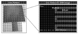
- FIG. 8 is a view illustrating an electrode pattern manufactured according to an embodiment. Specifically, FIG. 8 illustrates an entire image and an SEM image of a micro-zigzag pattern electrode structure.
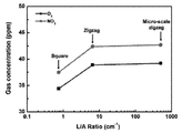
- FIG. 9 and 10 are views showing the effect of the electrode shape according to an embodiment of the present invention. Specifically, FIG. 9 shows the gas concentration according to the contour length, and FIG. 10 shows the concentration according to the ratio C / A of the contour length and the area.
- FIG. 9 and 10 in the case of the micro-zigzag pattern electrode structure manufactured using the lithography technique, the contour length was increased by 63 times more than that of the zigzag pattern electrode structure manufactured using the electroless plating. It can be seen that the concentrations of ozone and nitrogen dioxide gas produced are almost no difference. Therefore, it can be seen that optimal plasma characteristics can be obtained by using an inexpensive and easy method using an electroless plating method as in the present invention, without using a lithography and evaporation-deposition method having high manufacturing cost.
- the pattern electrode structure of the dielectric barrier discharge system of the present invention increases the contour length of the pattern electrode structure as the fine pattern is repeated and the size of the pattern is small.
- the discharge intensity of the dielectric barrier discharge plasma may be further increased compared to the pattern electrode structure having a relatively short contour length even when the same voltage is applied.
- contour length / area C / A
- C / A when C / A is lower than 1.6 cm -1 , the effect of increasing plasma discharge intensity may be relatively low, and as C / A increases by 1.6 cm -1 or more, The effect of increasing the plasma discharge intensity may also increase. At about 6.5 cm ⁇ 1 , the effect of increasing the plasma discharge intensity may be excellent.
- the C / A is 500cm -1 or more, there may be a problem that the manufacturing process cost increases significantly compared to the plasma discharge intensity increase degree.
- the dielectric barrier discharge system of the present invention can be applied to a small plasma apparatus or a bioplasma apparatus.
- the dielectric barrier discharge system includes a plasma chip, a plasma emission detector, a gas flow control, a plasma actuator, and a capillary plasma electrode (CPE) discharge. It can be applied to the back.
- CPE capillary plasma electrode
- carbon thin film generation and organic compound detection can be performed by plasma CVD, and frictional resistance can be reduced on the surface where air flow is generated.
- it can be used in the plasma reactor for chemical modification due to the molecular decomposition effect of the plasma generation, can also be used for the purification of volatile organic compounds.
- the contour length is relatively large compared to the area, it can be used in a small dielectric barrier discharge system and can also be used in the bio field.
- Plasma medical devices using the dielectric barrier discharge system of the present invention can be used for cell regeneration, sterilization, hemostasis and cancer cell death.
Landscapes
- Physics & Mathematics (AREA)
- Engineering & Computer Science (AREA)
- Plasma & Fusion (AREA)
- Spectroscopy & Molecular Physics (AREA)
- Plasma Technology (AREA)
Abstract
본 발명은 유전체 장벽 방전(dielectric barrier discharge, DBD) 플라즈마의 방전 세기를 조절하기 위한 무전해 도금을 이용하여 제조된 유전체 장벽 방전 시스템을 제공한다.
Description
본 발명은 유전체 장벽 방전 플라즈마에 관한 것으로, 보다 구체적으로는 유전체 장벽 방전 시스템에 관한 것이다.
유전체 장벽 방전(DBD) (Dielectric Barrier Discharge) 시스템은 간격이 있는 두 개의 전극에 높은 전압이 공급될 때 방전에 의해 두 개의 전극 사이에 생성되는 플라즈마를 이용하기 위한 장치이다.
유전체 장벽 방전 시스템은 두 개의 평행한 금속 전극으로 구성되어 있고, 전극 중 최소 한 개는 유전체층으로 덮여있다. 유전체 장벽 방전 시스템의 전극을 제조하기 위해서 원자층 증착(atomic layer deposition, ALD), 전자빔 증착(E-beam evaporation), 스퍼터(sputter), 리소그래피(lithography) 기술들이 이용될 수 있다. 또한 금속선(metal wire)과 금속필름(metal film)을 구부리거나 잘라내어서 전극을 제조할 수도 있다.
원자층 증착, 전자빔 증착, 스퍼터링, 리소그래피 등의 기술은 미세 전극 제조가 가능하다는 장점이 있지만, 고가의 장비가 필요하며, 전극 형성 속도가 느리다는 문제점들이 있다. 그리고 금속선 및 금속 필름을 이용하는 경우에는, 제조 방법이 간단하여 전극을 쉽게 제조할 수 있지만, 미세 전극 구조의 제조가 어렵다는 문제점이 있다. 결과적으로 이러한 문제점들을 해결할 수 있는 새로운 패턴 전극 제조 기술이 필요한 실정이다.
본 발명의 일 목적은 유전체 장벽 방전 플라즈마 방전 세기 조절되고, 보다 낮은 전압을 인가하여도 플라즈마 방전 세기가 우수하게 나타나는 유전체 장벽 방전 시스템을 제공하는 것이다.
본 발명의 일 목적을 위한 유전체 장벽 방전 시스템은 제2 전극 상에 형성된 유전체층; 상기 유전체층 상에 형성되고 패턴을 갖는 패턴 시드층; 및 상기 패턴 시드층 상에 형성되고, 패턴을 갖는 패턴 금속층;을 포함한다.
일 실시예에서 상기 패턴 금속층의 패턴은 윤곽길이(Contour length)/면적(Area) 비율(C/A)이 1.3cm-1 내지 500cm-1 일 수 있다.
일 실시예에서 상기 패턴 금속층은 지그재그(zigzag) 패턴으로 형성된 것일 수 있다.
일 실시예에서 상기 패턴 시드층의 두께는 1nm 내지 10nm일 수 있다.
일 실시예에서 상기 유전체 장벽 방전 시스템은 소형 플라즈마 장치 및 플라즈마 의학 분야에서 사용될 수 있다.
본 발명의 유전체 장벽 방전 시스템은 종래 기술보다 공정 비용이 저렴하여 경제적이고, 생산성이 높으며, 패턴의 윤곽길이가 증가하여, 상대적으로 낮은 전압을 인가하여도, 플라즈마 방전 세기를 증가시킬 수 있다. 이러한 본 발명의 유전체 장벽 방전 시스템은 플라즈마 의학(plasma medicine), 플라즈마 액츄에이터(plasma actuator), 마이크로 반응기(micro reactor) 등 다양한 분야에서 응용성을 나타낼 수 있다.
도 1은 본 발명의 일 실시예에 따른 유전체 장벽 방전 시스템의 제조 방법 일부를 나타낸 개략도이다.
도 2는 본 발명의 일 실시예에 따른 시드층 패턴을 나타낸 도면이다.
도 3은 본 발명의 일 실시예에 따른 무전해 도금 시간별 패턴 금속층 표면을 나타낸 도면이다.
도 4는 본 발명의 일 실시예에 따른 유전체 장벽 방전 시스템의 개략도를 나타낸 도면이다.
도 5 내지 도 7은 본 발명의 일 실시예에 따른 유전체 장벽 방전 시스템의 플라즈마 특성을 나타낸 도면들이다.
도 8은 일 실시예에 따라 제조된 전극 패턴을 나타낸 도면이다.
도 9 및 도 10은 본 발명의 일 실시예에 따른 전극 형태에 따른 효과를 나타낸 도면들이다.
본 출원에서 사용한 용어는 단지 특정한 실시 예를 설명하기 위해 사용된 것으로서 본 발명을 한정하려는 의도가 아니다. 단수의 표현은 문맥상 명백하게 다르게 뜻하지 않는 한, 복수의 표현을 포함한다. 본 출원에서, "포함하다" 또는 "가지다" 등의 용어는 명세서 상에 기재된 특징, 단계, 동작, 구성요소, 부분품 또는 이들을 조합한 것이 존재함을 지정하려는 것이지, 하나 또는 그 이상의 다른 특징들이나 단계, 동작, 구성요소, 부분품 또는 이들을 조합한 것들의 존재 또는 부가 가능성을 미리 배제하지 않는 것으로 이해되어야 한다.
다르게 정의되지 않는 한, 기술적이거나 과학적인 용어를 포함해서 여기서 사용되는 모든 용어들은 본 발명이 속하는 기술 분야에서 통상의 지식을 가진 자에 의해 일반적으로 이해되는 것과 동일한 의미를 가지고 있다. 일반적으로 사용되는 사전에 정의되어 있는 것과 같은 용어들은 관련 기술의 문맥 상 가지는 의미와 일치하는 의미를 가지는 것으로 해석되어야 하며, 본 출원에서 명백하게 정의하지 않는 한, 이상적이거나 과도하게 형식적인 의미로 해석되지 않는다.
본 발명은 플라즈마의 방전 세기가 증가된 유전체 장벽 방전(dielectric barrier discharge, DBD) 시스템에 관한 것이다. 전극의 가장자리(윤곽)에서 보다 더 강한 전기장이 형성되는데, 본 발명의 유전체 장벽 방전 시스템은 상기 시스템에 포함된 전극에 패턴을 형성함으로서 전극의 윤곽길이(Contour length)를 증가시키고, 이로 인해 상대적으로 낮은 전압을 인가하여도 보다 높은 세기의 플라즈마를 얻을 수 있다. 다시말해서 본 발명의 유전체 장벽 방전 시스템은 전극의 패턴 형태를 조절함으로써 플라즈마 세기를 조절할 수 있다.
본 발명의 유전체 장벽 방전 시스템은 제2 전극 상에 형성된 유전체층; 상기 유전체층 상에 형성되고 패턴을 갖는 패턴 시드층; 및 상기 패턴 시드층 상에 형성되고, 패턴을 갖는 패턴 금속층;을 포함한다.
일 실시예에서 상기 유전체 장벽 방전 시스템은 상기 제2 전극, 상기 유전체층, 상기 패턴 시드층, 상기 패턴 금속층이 순서대로 적층된 구조를 포함할 수 있다. 이때, 상기 패턴 금속층은 패턴을 갖는 제1 전극을 의미한다.
일 실시예에서 상기 제2 전극은 상기 패턴 금속층과 동일한 금속을 포함할 수 있고, 서로 다른 금속을 포함할 수 있다. 예를 들어 상기 패턴 금속층은 구리를 포함하고, 상기 제2 전극은 철을 포함할 수 있으며, 상기 제2 전극은 철망이 사용될 수 있다.
*일 실시예에서 상기 유전체층은 유전상수가 높은 물질을 포함할 수 있고, 상기 패턴 시드층 및 패턴 금속층은 금속을 포함할 수 있다. 예를 들어 상기 유전체층은 석영, 유리, 알루미나(산화알루미늄), 티타니아(산화티타늄), 지르코니아(산화지르코늄), 산화아연, 산화철, 카본나노튜브 등을 포함할 수 있고 상기 금속은 금, 은, 백금, 구리, 알루미늄, 텅스텐 및 이들의 합금등을 포함할 수 있다. 일 실시예에서 상기 패턴 시드층 및 상기 패턴 금속층은 동일한 금속을 포함할 수 있고, 서로 다른 금속을 포함할 수 있다. 예를 들어 상기 패턴 시드층은 금을 포함하고, 상기 패턴 금속층은 구리를 포함할 수 있다. 상기 패턴 시드층은 백금 또는 팔라듐을 이용하여 형성할 수 있다. 이때 백금 또는 팔라듐은 불소가 포함된 용액에서 시드층을 형성하게 되어 위험성이 높고 재료의 가격이 높아 비용이 크게 사용되는 단점이 있다. 스퍼터링으로 금을 이용하여 상기 패턴 시드층을 형성하게 되면, 백금 또는 팔라듐을 이용하는 것보다는 상대적으로 공정이 간다하며 비교적 저렴한 비용으로 제조가 가능하다. 또한 상기 패턴층은 구리, 금, 은, 백금 등 전도성이 큰 금속으로 형성될 수 있으나, 이중에서 구리를 이용하여 상기 패턴 금속층을 형성하는 경우에는, 전도성이 크면서도 제조 비용이 저렴하다는 장점이 있다.
일 실시예에서 상기 패턴 금속층의 패턴은 윤곽길이(Contour length)/면적(Area) 비율(C/A)이 1.3cm-1 내지 500cm-1일 수 있다. 예를 들어 상기 패턴의 윤곽길이/면적 비율은 6.5cm-1 내지 500cm-1일 수 있다. 상기 윤곽길이/면적 비율인, C/A가 1.3 cm-1 미만인 경우, 플라즈마 세기가 증가하는 효과가 크게 나타나지 않을 수 있으며, C/A가 500 cm-1 이 넘는 경우에는 플라즈마 세기가 증가하는 효과에 비해 제조 비용이 크게 증가하고 공정이 상대적으로 어려운 문제점이 발생할 수 있다.
일 실시예에서 상기 패턴 금속층의 패턴은 이에 제한하는 것이 아니라, 사각(Square)형, 덤벨(Dumbbell)형, 톱(Saw)형, 별(Star)형, 지그재그(zigzag)형 등 다양한 패턴으로 형성될 수 있다. 예를 들어 상기 패턴 금속층은 지그재그형 패턴일 수 있다.
일 실시예에서 상기 패턴 금속층의 두께는 100nm 내지 50μm 일 수 있다.
일 실시예에서 상기 패턴 시드층의 두께는 1nm 내지 10nm 일 수 있다. 예를 들어 상기 패턴 시드층의 두께가 1nm 미만인 경우, 상기 패턴 시드층이 안정적으로 유지되기 어려울 수 있고, 상기 패턴 시드층 상에 상기 패턴 금속층이 적층되기 어려울 수 있으며, 또한, 상기 패턴 시드층의 두께가 10nm보다 두꺼운 경우에는 제조 공정 상에서 다양한 문제점이 발생할 수 있고, 플라즈마 세기 증가 효과가 상대적으로 미미하게 나타나는 문제점이 발생할 수 있다.
본 발명의 유전체 장벽 방전 시스템에 포함되는 패턴 전극 구조체의 제조 방법은 유전체층 상에 패턴 시드(seed)층을 형성하는 제1 단계; 및 무전해 도금을 통해 상기 패턴 시드층 상에 패턴 금속층을 형성하는 제2 단계;를 포함한다.
일 실시예에서 상기 제1 단계는 유전체 박막 또는 유전체 층 표면에 시드층을 형성하는 단계일 수 있다. 일 실시예에서 상기 시드층은 일정한 패턴을 갖는 상기 패턴 시드층일 수 있다. 일 실시예에서 상기 유전체는 유전상수가 높은 세라믹, 고분자 일 수 있으며, 이에 제한하지 않고 사용할 수 있다.
일 실시예에서 상기 제1 단계는 스퍼터링을 통해 상기 유전체 표면에 상기 패턴 시드층을 형성하는 것 일 수 있다. 일 실시예에서 상기 패턴 시드층을 형성하기 위해서 유전체층 상에 패턴 마스크를 위치시킨 다음, 시드층 물질을 증착시켜 상기 패턴 시드층을 형성할 수 있다. 일 실시예에서 스퍼터링을 통해 상기 패턴 마스크의 열린 공간에만 상기 시드층 물질이 증착될 수 있다.
일 실시예에서 상기 시드층 물질은 금, 은, 백금, 구리, 아연, 니켈, 코발트, 인, 망간 등이 사용될 수 있으며, 이에 제한하지 않고, 무전해 도금의 시드층 역할이 가능한 다양한 물질들이 사용될 수 있다.
일 실시예에서 상기 패턴 마스크는 3D 프린터를 이용하여 간단하게 제조될 수 있다. 일 실시예에서 상기 패턴 시드층의 패턴 크기는 상기 패턴 마스크의 크기 및 형태에 따라 다양하게 조절할 수 있고 상기 패턴 마스크는 스퍼터링 공정 후 제거될 수 있고, 재사용 될 수 있다.
일 실시예에서 스퍼터링의 시간 및/또는 전류량을 조절함으로서 상기 시드층의 두께를 조절할 수 있다. 일 예로 상기 패턴 시드층의 두께가 1nm 내지 10nm 가 되도록 스퍼터링 조건을 조절할 수 있다.
일 실시예에서 상기 제2 단계는 무전해 도금을 통해서 상기 패턴 시드층 상에 금속을 증착시켜 상기 패턴 금속층을 형성하는 것일 수 있다.
일 실시예에서 상기 무전해 도금을 하기 위해 무전해 도금 욕을 제조할 수 있으며, 무전해 도금에 사용되는 물질을 제한하지 않고 사용할 수 있다. 예를 들어 구리 무전해 도금 욕을 제조하기 위해서는 구리를 포함하는 물질이 사용될 수 있다. 예를 들어 상기 제2 단계의 무전해 도금은 구리를 포함하는 물질을 이용한 무전해 도금일 수 있다.
일 실시예에서 상기 무전해 도금을 위한 도금 온도는 50℃ 내지 90℃일 수 있다. 예를 들어 상기 도금 온도는 70℃일 수 있다. 65℃ 이하의 온도에서는 도금 속도가 느려지는 문제점이 발생할 수 있으며, 75℃ 이상의 온도에서는 도금 용액이 증발하는 문제점이 발생할 수 있다.
일 실시예에서 상기 무전해 도금 욕의 pH 범위는 11 내지 13일 수 있다. 예를 들어 상기 무전해 도금 욕은 pH 12일 수 있다. pH가 11 이하인 경우에는 도금 속도가 현저히 감소하는 문제점이 발생할 수 있다.
일 실시예에서 상기 무전해 도금 공정 시간은 0.1분 내지 30분 동안 수행되는 것일 수 있다.
도 1은 본 발명의 일 실시예에 따른 유전체 장벽 방전 시스템의 제조 방법 일부를 나타낸 개략도이다. 일 실시예에서 본 발명의 유전체 장벽 방전 시스템을 제조하기 위해 먼저, 스퍼터링을 통해 유전체 표면에 패턴 시드층을 형성한 다음, 구리 무전해 도금 욕을 제조하고, 제조된 상기 구리 무전해 도금 욕을 이용하여 상기 패턴 시드층 상에 구리 박막을 도금하는 공정을 수행하여 유전체 장벽 방전 시스템에 사용가능한 패턴 전극 구조체를 제조할 수 있다.
도 2는 본 발명의 일 실시예에 따른 패턴 시드층의 패턴을 나타낸 도면이다. 일 실시예에서 상기 패턴 마스크를 통해 다양한 형태의 패턴을 갖는 패턴 시드층을 형성할 수 있고, 형성 가능한 패턴의 예를 도 2에 나타내었다. 예를 들어 상기 패턴 시드층의 패턴은 사각형, 덤벨형, 톱형, 별형, 지그재그형 등이 있다.
실시예
무전해 도금 욕 제조
본 발명의 실시예에 따라 무전해 도금 욕을 제조하였다. 구리 무전해 도금 욕은 2차 증류수에 CuSO4·5H2O(9g/L), HCHO(8.5g/L), 에틸렌 디아민 테트라 아세트산 테트라 소듐 염 하이드레이트(Ethylenediaminetetraacetic acid tetrasodium salt hydrate)(35g/L)를 용해하여 제조하였다. 상온에서 1M의 NaOH 용액을 이용하여 상기 도금 욕의 pH를 12로 조절하였다.
유전체 장벽 방전 시스템용 패턴 전극 구조체 제조
본 발명의 일 실시예에 따라 유전체 장벽 방전 시스템용 패턴 전극 구조체를 제조하였다. 이때 유전체로는 지르코니아 플레이트(zirconia plate)를 사용하였다.
먼저, 지르코니아 플레이트 표면 상에 패턴 마스크를 위치시킨 다음, 이온 스퍼터(ion sputter) 기기에서 20초 동안 4mA를 인가하여 지르코니아 플레이트 표면에 금 시드층을 증착함으로서 패턴 시드층을 형성하였다.
그리고 제조된 상기 패턴 시드층 상에 구리 박막을 형성하기 위해서, 구리 무전해 도금을 수행하였다. 이때, 본 발명의 일 실시예에 따라 제조된 구리 무전해 도금 욕을 사용하였고, 교반 속도는 150rpm, 도금 온도는 70℃으로 조절하였다. 상기 구리 무전해 도금 욕에 상기 시드층이 형성된 지르코니아 플레이트를 담그고 일정 시간 이후 꺼내어 세척과 건조를 실시하였다. 제조 시, 패턴 형태와 관계없이 구리 박막의 면적은 약 9.5cm2로 비슷하게 제조되어 면적이 플라즈마 세기에 미치는 영향은 최소화하였다. 본 발명의 패턴 전극 구조체는 상기 패턴 시드층 위에 상기 패턴 금속층이 형성되는 것, 예를 들어 패턴을 갖는 금 패턴 시드층 상에 구리 박막이 도금되는 것이므로 구리 박막의 패턴은 금 패턴 시드층의 패턴과 동일하게 나타났다.
도 3은 본 발명의 일 실시예에 따른 무전해 도금 시간별 패턴 금속층 표면을 나타낸 도면이다. 구체적으로 도 3은 본 발명의 일 실시예에 따라 유전체층이 지르코니아 플레이트, 패턴 시드층이 금 시드층, 패턴 금속층이 구리 박막인 패턴 전극 구조체의 무전해 도금 시간별 패턴 금속층, 다시말해서 무전해 도금 시간별 구리 박막의 표면 변화를 나타낸 것이다. 약 5분 간 무전해 도금을 수행하였을 때, 지르코니아 플레이트 표면에 균일한 형상의 구리 박막이 형성되었으며 약 8μm 두께로 표면 전체에 패턴이 형성되었다.
본 발명의 유전체 장벽 방전 시스템에 따른 플라즈마의 방전 세기를 비교하기 위해서 상기 실시예를 통해 제조된 상기 패턴 전극 구조체를 이용하여 본 발명의 유전체 장벽 방전 시스템을 제조하였다. 도 4는 본 발명의 일 실시예에 따른 유전체 장벽 방전 시스템을 개략적으로 나타낸 도면이다. 먼저 도 4의 (a)에 나타낸 유전체 장벽 방전 시스템은 본 발명의 일 실시예에 따라 제조된 패턴 전극 구조체를 포함하며, 구체적으로 기판, 패턴 금속층, 유전체층, 제2 전극을 포함한다. 도 4의 (a)에서 상기 패턴 금속층은 본 발명의 패턴 전극 구조체의 패턴 금속층을 나타내는 것으로, 도 4의 (a)의 상기 패턴 금속층 및 유전체층이 본 발명의 패턴 전극 구조체의 일 예이다. 도 4의 (b)에 나타낸 유전체 장벽 방전 시스템은 본 발명의 일 실시예에 따라 제조된 패턴 전극 구조체를 포함하며, 구체적으로 테프론 기판, 상기 패턴 금속층으로 패턴을 갖는 구리 박막 그리고 유전체층으로 지르코니아 플레이트를 포함하는 패턴 전극 구조체, 그리고 제2 전극으로 철망(SUS mesh)을 포함하고, 각각의 두께는 도 4에 나타내었다.
방전 세기를 비교하기 위해서, 일 실시예에 따라 제조된 유전체 장벽 방전 시스템에 25 kHz 주파수의 AC 파워를 15 kV로 인가하였다. 이 때, 방전 가스는 별도의 가스를 사용하지 않고 대기를 이용하여 방전시켰다. 그리고 온도는 25℃로 일정하게 유지하였다. 비교 결과, 다양한 형태의 패턴 전극 구조체에서 안정적인 플라즈마가 방전되었으며, 다양한 형태의 패턴 전극 구조체에 따른 플라즈마의 세기는 광학적 분석 장비인 OES(optical emission spectroscopy)를 이용하여 구체적으로 비교되었다.
도 5 내지 도 7은 본 발명의 일 실시예에 따른 유전체 장벽 방전 플라즈마 특성을 나타낸 도면들로, 다양한 패턴 전극 구조체를 사용하여 제작한 유전체 장벽 방전 시스템에 동일한 전압을 인가하였을 때, 발생되는 플라즈마의 특성을 분석한 결과를 나타낸 것이다. 구체적으로 도 5는 본 발명의 일 실시예에 따른 유전체 장벽 방전 플라즈마 특성을 나타낸 도면으로, 도 5의 (a)는 패턴 전극 구조체의 형태에 따른 유전체 장벽 방전 플라즈마의 OES 스펙트럼 결과, 도 5의 (b)는 각 패턴의 윤곽길이와 플라즈마 세기를 나타낸 것이다. 비교 결과, 패턴의 윤곽 길이가 증가함에 따라 OES 스펙트럼의 피크 세기(peak intensity)가 증가하였고, 윤곽길이가 증가할수록 플라즈마 세기가 증가하는 것을 알 수 있었다. 또한 패턴의 형태는 다르지만 면적과 윤곽길이가 동일한 톱형(Saw)와 별형(Star) 패턴의 경우에는 OES 스펙트럼의 피크 세기가 비슷하게 나타났다. 따라서 플라즈마 세기가 패턴의 형태보다는 윤곽길이에 영향을 받는 것을 알 수 있다.
구체적으로 도 6은 본 발명의 일 실시예에 따른 패턴 전극 구조체의 윤곽길이에 따른 플라즈마에서 생성된 가스의 농도를 나타낸 것이다. 패턴 전극 구조체의 패턴의 윤곽길이가 증가할 때, 오존(O3)과 이산화질소(NO2)의 농도가 증가한 것을 알 수 있다. 플라즈마 방전 세기가 증가하면, 플라즈마 내 화학종의 농도가 증가하여 가스 생성을 위한 반응속도가 증가할 수 있다. 따라서 패턴 전극 구조체의 윤곽길이 증가는 플라즈마 세기를 향상시키므로 생성되는 반응 가스의 농도를 증가시킬 수 있다.
그리고 도 7은 본 발명의 일 실시예에 따른 패턴 전극 구조체의 윤곽길이에 따른 전자온도의 변화를 나타낸 것이다. 패턴 전극 구조체의 윤곽길이가 증가함에 따라 전자온도가 증가하는 것을 알 수 있다. 전기장의 세기가 강할수록 전자는 더욱 많은 에너지를 축적할 수 있으므로 전자온도가 증가한다. 도 7을 보면 윤곽길이가 증가할수록 전자온도가 증가하므로 윤곽길이가 증가할수록 전기장의 세기가 강해지는 것을 알 수 있다. 결과적으로 본 발명을 통해서 동일한 전압을 인가하더라도 패턴 전극 구조체의 윤곽길이가 증가될 경우, 플라즈마 세기, 발생하는 가스의 농도 및 전자온도가 증가하는 것을 알 수 있다.
일 실시예를 통해 제조된 각 패턴별 패턴 전극 구조체의 윤곽길이와 면적의 비(C/A)는 사각형(Square)이 1.3cm-1, 덤벨형(Dumbbell)이 1.6cm-1, 톱형(Saw)이 3.9cm-1, 별형(Star)이 3.9cm-1 그리고 지그재그형(Zigzag)이 6.7cm-1였다. 윤곽길이와 면적의 비가 1.6 cm-1 미만인 경우에는 윤곽길이에 따른 플라즈마 특성 변화가 상대적으로 크게 나타났다. 반면 C/A가 1.6 cm-1 이상인 경우에는 윤곽길이에 따른 플라즈마 특성의 변화폭이 점차 감소하여, 3.9 cm-1 이상인 경우에는 윤곽길이에 따른 특성 변화가 상대적으로 작게 나타났다.
위에서 확인한 것과 같이, 윤곽길이에 대한 플라즈마 세기 변화를 확인해보기위해 지그재그형 패턴 전극 구조체와 마이크로 사이즈의 지그재그형(Micro-scale zigzag) 패턴 전극구조체를 제조하여 비교하였다. 아래 표 1에 사각형, 지그재그형 및 마이크로 사이즈 지그재그형(Micro-지그재그)의 면적과 윤곽길이를 나타내었다.
| 구분 | 사각 | 지그재그 | micro-지그재그 |
| 면적(cm2) | 9.00 | 9.69 | 8.00 |
| 윤곽길이(cm) | 12.0 | 63.2 | 4000 |
일 실시예에서 Micro-지그재그형 패턴 전극 구조체는 선폭을 마이크로 사이즈로 감소시키기위해, 고가의 리소그래피(lithography) 기술을 이용하여 패턴 마스크를 형성한 다음, 금을 evaporation-증착하여 제조하였다.
도 8은 일 실시예에 따라 제조된 전극 패턴을 나타낸 도면으로, 구체적으로는 Micro-지그재그형 패턴 전극 구조체의 전체 이미지와 SEM 이미지를 나타낸 것이다.
도 9 및 도 10은 본 발명의 일 실시예에 따른 전극 형태에 따른 효과를 나타낸 도면들이다. 구체적으로 도 9는 윤곽길이에 따른 가스 농도, 도 10은 윤곽길이와 면적의 비(C/A)에 따른 농도를 나타낸 것이다. 도 9 및 도 10을 보면, 리소그래피 기술을 이용하여 제조된 Micro-지그재그형 패턴 전극 구조체의 경우, 윤곽길이가 무전해 도금을 이용하여 제조된 지그재그형 패턴 전극 구조체 보다 63배 이상 증가되었으나, 플라즈마에서 생성되는 오존 및 이산화질소 가스의 농도는 거의 차이가 없는 것을 알 수 있다. 따라서 제작비용이 높은 리소그래피 및 evaporation-증착 방법을 사용하지 않고, 본 발명과 같이 무전해 도금 방법을 이용하여 저렴하고 쉬운 방법을 통해 최적의 플라즈마 특성을 얻을 수 있다는 것을 알 수 있다.
결과적으로 본 발명의 유전체 장벽 방전 시스템의 패턴 전극 구조체는 미세 패턴이 반복되고 패턴의 크기가 작을수록 상기 패턴 전극 구조체의 윤곽길이가 증가되는 것을 알 수 있다. 그리고 패턴 전극 구조체의 윤곽길이가 증가되면 동일한 전압을 인가하더라도 상대적으로 윤곽길이가 짧은 패턴 전극 구조체에 비해서 유전체 장벽 방전 플라즈마의 방전 세기를 더 증가시킬 수 있다. 이를 윤곽길이/면적(C/A)으로 나타내면, C/A가 1.6cm-1 보다 낮은 경우에는 플라즈마 방전 세기 증가의 효과가 상대적으로 낮게 나타날 수 있으며, C/A가 1.6cm-1 이상 증가할수록 플라즈마 방전 세기 증가 효과 역시 증가할 수 있다. 6.5cm-1 정도에서 플라즈마 방전 세기 증가 효과가 우수하게 나타날 수 있다. 또한 C/A가 500cm-1 이상인 경우, 플라즈마 방전 세기 증가 정도에 비해 제조 공정 비용이 크게 증가하는 문제점이 발생할 수 있다.
본 발명의 유전체 장벽 방전 시스템은 소형 플라즈마 장치 또는 바이오 플라즈마 장치에 응용이 가능하다. 일 실시예에서 상기 유전체 장벽 방전 시스템은 플라즈마 칩(Plasma chip), 플라즈마 방출 검출기(Molecular emission detector), 기체 흐름 제어, 플라즈마 반응기(plasma actuator), 모세관 플라즈마 전극(Capillary plasma electrode (CPE) discharge) 방전 등에 응용 가능하다. 구체적으로 본 발명의 유전체 장벽 방전 시스템을 이용해서, 플라즈마 CVD 방식으로 탄소 박막 생성 및 유기화합물 검출이 가능하며, 공기 흐름이 발생하는 표면에서 마찰에 의한 저항력을 감소시킬 수 있다. 또한 플라즈마 반응기에 사용하여 플라즈마 발생으로 인한 분자 분해 효과로 화학적 변형에 사용될 수 있으며, 휘발성 유기 화합물의 정화에도 사용될 수 있다. 또한 면적에 비해 윤곽길이가 상대적으로 큰 특징을 나타내므로 소형 유전체 장벽 방전 시스템에 사용할 수 있으며, 바이오 분야에서도 사용될 수 있다. 본 발명의 유전체 장벽 방전 시스템을 이용한 플라즈마 의학기기의 경우 세포의 재생, 살균, 지혈 및 암세포 사멸 등을 위해 사용될 수 있다.
상기에서는 본 발명의 바람직한 실시예를 참조하여 설명하였지만, 해당 기술 분야의 숙련된 당업자는 하기의 특허 청구 범위에 기재된 본 발명의 사상 및 영역으로부터 벗어나지 않는 범위 내에서 본 발명을 다양하게 수정 및 변경시킬 수 있음을 이해할 수 있을 것이다.
Claims (7)
- 제2 전극 상에 형성된 유전체층;상기 유전체층 상에 형성되고 패턴을 갖는 패턴 시드층; 및상기 패턴 시드층 상에 형성되고, 패턴을 갖는 패턴 금속층;을 포함하는,유전체 장벽 방전 시스템.
- 제1항에 있어서,상기 패턴 금속층의 패턴은 윤곽길이(Contour length)/면적(Area) 비율(C/A)이 1.3cm-1 내지 500cm-1인 것을 특징으로 하는,유전체 장벽 방전 시스템.
- 제2항에 있어서,상기 패턴 금속층은 지그재그(zigzag) 패턴으로 형성된 것을 특징으로 하는,유전체 장벽 방전 시스템.
- 제1항에 있어서,상기 패턴 시드층의 두께는 1nm 내지 10nm인 것을 특징으로 하는,유전체 장벽 방전 시스템.
- 제1항에 있어서,상기 유전체 장벽 방전 시스템은 플라즈마 의학기기에 사용되는 것을 특징으로 하는,유전체 장벽 방전 시스템.
- 제1항에 있어서,상기 유전체 장벽 방전 시스템은 플라즈마 액츄에이터(plasma actuator)에 사용되는 것을 특징으로 하는,유전체 장벽 방전 시스템.
- 제1항에 있어서,상기 유전체 장벽 방전 시스템은 마이크로 반응기에 사용되는 것을 특징으로 하는,유전체 장벽 방전 시스템.
Applications Claiming Priority (2)
| Application Number | Priority Date | Filing Date | Title |
|---|---|---|---|
| KR1020180093899A KR20200018101A (ko) | 2018-08-10 | 2018-08-10 | 유전체 장벽 방전 시스템 |
| KR10-2018-0093899 | 2018-08-10 |
Publications (1)
| Publication Number | Publication Date |
|---|---|
| WO2020032352A1 true WO2020032352A1 (ko) | 2020-02-13 |
Family
ID=69414203
Family Applications (1)
| Application Number | Title | Priority Date | Filing Date |
|---|---|---|---|
| PCT/KR2019/005871 Ceased WO2020032352A1 (ko) | 2018-08-10 | 2019-05-16 | 유전체 장벽 방전 시스템 |
Country Status (2)
| Country | Link |
|---|---|
| KR (1) | KR20200018101A (ko) |
| WO (1) | WO2020032352A1 (ko) |
Citations (5)
| Publication number | Priority date | Publication date | Assignee | Title |
|---|---|---|---|---|
| JP2006253118A (ja) * | 2005-02-10 | 2006-09-21 | Konica Minolta Holdings Inc | プラズマ放電処理用ガス、プラズマ放電処理用ガスの生成方法およびプラズマ放電処理方法 |
| JP2012518256A (ja) * | 2009-02-17 | 2012-08-09 | マックス プランク ゲゼルシャフト ツゥアー フェデルゥン デル ヴィッセンシャフテン エー フォー | 非熱プラズマを生成するための電極列 |
| KR20130081687A (ko) * | 2013-06-27 | 2013-07-17 | 박진옥 | 오존 및 프리라디칼 생성장치 및 이를 이용한 미생물 제거 시스템 |
| KR20150031763A (ko) * | 2013-09-16 | 2015-03-25 | 한국기계연구원 | 표면 처리를 위한 유전체 장벽 방전 반응기 |
| KR20170040654A (ko) * | 2015-10-05 | 2017-04-13 | 주식회사 에프티넷 | 연면방전과 공간방전을 동시에 사용하는 복합형 유전체 장벽 방전 전극 |
-
2018
- 2018-08-10 KR KR1020180093899A patent/KR20200018101A/ko not_active Ceased
-
2019
- 2019-05-16 WO PCT/KR2019/005871 patent/WO2020032352A1/ko not_active Ceased
Patent Citations (5)
| Publication number | Priority date | Publication date | Assignee | Title |
|---|---|---|---|---|
| JP2006253118A (ja) * | 2005-02-10 | 2006-09-21 | Konica Minolta Holdings Inc | プラズマ放電処理用ガス、プラズマ放電処理用ガスの生成方法およびプラズマ放電処理方法 |
| JP2012518256A (ja) * | 2009-02-17 | 2012-08-09 | マックス プランク ゲゼルシャフト ツゥアー フェデルゥン デル ヴィッセンシャフテン エー フォー | 非熱プラズマを生成するための電極列 |
| KR20130081687A (ko) * | 2013-06-27 | 2013-07-17 | 박진옥 | 오존 및 프리라디칼 생성장치 및 이를 이용한 미생물 제거 시스템 |
| KR20150031763A (ko) * | 2013-09-16 | 2015-03-25 | 한국기계연구원 | 표면 처리를 위한 유전체 장벽 방전 반응기 |
| KR20170040654A (ko) * | 2015-10-05 | 2017-04-13 | 주식회사 에프티넷 | 연면방전과 공간방전을 동시에 사용하는 복합형 유전체 장벽 방전 전극 |
Also Published As
| Publication number | Publication date |
|---|---|
| KR20200018101A (ko) | 2020-02-19 |
Similar Documents
| Publication | Publication Date | Title |
|---|---|---|
| DE69733530T3 (de) | Flexibler verbundstoff ohne klebstoff und verfahren zu seiner herstellung | |
| KR102626372B1 (ko) | Rf 집적형 전력 조절 커패시터 | |
| US7455757B2 (en) | Deposition method for nanostructure materials | |
| DE69607967T2 (de) | ELEKTROKATALYTISCHE STRUKTUR MIT EINER MATRIX AUS SiOxCyHz UND DARIN EINGEBETTETEN TEILCHEN AUS KATALYTISCH AKTIVEM MATERIAL | |
| US4557796A (en) | Method of dry copper etching and its implementation | |
| DE3402971C2 (ko) | ||
| KR20060125883A (ko) | 접착 본드 및 그 제조 방법 | |
| Mahajan et al. | Carbon nanotube–nanocrystal heterostructures fabricated by electrophoretic deposition | |
| WO2018038495A1 (ko) | 나노포러스 구조 막 형성용 스퍼터링 장치 | |
| DE3874069T2 (de) | Oberflaechenbehandlung von polymeren. | |
| EP1264330B1 (de) | Verfahren und vorrichtung zur plasmagestützten oberflächenbehandlung und verwendung des verfahrens | |
| WO2017039055A1 (ko) | 그래핀 복합 금속와이어 및 그의 제조방법 | |
| WO2020032352A1 (ko) | 유전체 장벽 방전 시스템 | |
| KR20220142535A (ko) | 초고표면적 집적 커패시터 | |
| EP3142467A1 (en) | Large area, uniform, atmospheric pressure plasma processing device | |
| EP4105359A1 (de) | Ionen-austausch-membran, verfahren zum herstellen der ionen-austausch-membran, elektrolyse-vorrichtung mit der ionen-austausch-membran und verwendung der elektrolyse-vorrichtung | |
| CN110806130B (zh) | 电沉积蒸发器的环路热管及其制备方法 | |
| JP3145764B2 (ja) | 導体コイルパターンの製造方法及び製造装置 | |
| EP0087151A2 (de) | Verfahren zum Herstellen von Schichten aus hochschmelzenden Metallen bzw. Metallverbindungen durch Abscheidung aus der Dampfphase | |
| CN101532177B (zh) | 用模板法制备硫化锌量子线的方法 | |
| CN1535110A (zh) | 防电磁干扰遮蔽罩的制造方法 | |
| KR102665090B1 (ko) | 마이크로 히터 제작을 위한 투명전극 제작 공정 방법 | |
| WO1989010336A1 (en) | Superconducting ceramics by electrodeposition | |
| KR102660721B1 (ko) | 유리기판 상에 금속 박막을 형성하는 방법 | |
| CN112601840B (zh) | 金属膜形成用组合物的制造方法、金属膜的制造方法、金属膜、金属膜层叠体和金属膜形成用组合物的制造装置 |
Legal Events
| Date | Code | Title | Description |
|---|---|---|---|
| 121 | Ep: the epo has been informed by wipo that ep was designated in this application |
Ref document number: 19847624 Country of ref document: EP Kind code of ref document: A1 |
|
| NENP | Non-entry into the national phase |
Ref country code: DE |
|
| 122 | Ep: pct application non-entry in european phase |
Ref document number: 19847624 Country of ref document: EP Kind code of ref document: A1 |