WO2019176209A1 - 固体撮像装置 - Google Patents
固体撮像装置 Download PDFInfo
- Publication number
- WO2019176209A1 WO2019176209A1 PCT/JP2018/046505 JP2018046505W WO2019176209A1 WO 2019176209 A1 WO2019176209 A1 WO 2019176209A1 JP 2018046505 W JP2018046505 W JP 2018046505W WO 2019176209 A1 WO2019176209 A1 WO 2019176209A1
- Authority
- WO
- WIPO (PCT)
- Prior art keywords
- pixel
- incident
- light
- unit
- imaging device
- Prior art date
- Legal status (The legal status is an assumption and is not a legal conclusion. Google has not performed a legal analysis and makes no representation as to the accuracy of the status listed.)
- Ceased
Links
Images


Classifications
-
- G—PHYSICS
- G02—OPTICS
- G02B—OPTICAL ELEMENTS, SYSTEMS OR APPARATUS
- G02B5/00—Optical elements other than lenses
- G02B5/20—Filters
-
- G—PHYSICS
- G02—OPTICS
- G02B—OPTICAL ELEMENTS, SYSTEMS OR APPARATUS
- G02B5/00—Optical elements other than lenses
- G02B5/30—Polarising elements
-
- H—ELECTRICITY
- H04—ELECTRIC COMMUNICATION TECHNIQUE
- H04N—PICTORIAL COMMUNICATION, e.g. TELEVISION
- H04N23/00—Cameras or camera modules comprising electronic image sensors; Control thereof
- H04N23/10—Cameras or camera modules comprising electronic image sensors; Control thereof for generating image signals from different wavelengths
- H04N23/12—Cameras or camera modules comprising electronic image sensors; Control thereof for generating image signals from different wavelengths with one sensor only
-
- H—ELECTRICITY
- H04—ELECTRIC COMMUNICATION TECHNIQUE
- H04N—PICTORIAL COMMUNICATION, e.g. TELEVISION
- H04N25/00—Circuitry of solid-state image sensors [SSIS]; Control thereof
- H04N25/70—SSIS architectures; Circuits associated therewith
-
- H—ELECTRICITY
- H10—SEMICONDUCTOR DEVICES; ELECTRIC SOLID-STATE DEVICES NOT OTHERWISE PROVIDED FOR
- H10F—INORGANIC SEMICONDUCTOR DEVICES SENSITIVE TO INFRARED RADIATION, LIGHT, ELECTROMAGNETIC RADIATION OF SHORTER WAVELENGTH OR CORPUSCULAR RADIATION
- H10F39/00—Integrated devices, or assemblies of multiple devices, comprising at least one element covered by group H10F30/00, e.g. radiation detectors comprising photodiode arrays
- H10F39/10—Integrated devices
- H10F39/12—Image sensors
Definitions
- This technology relates to a solid-state imaging device so that polarization information can be obtained for each color component.
- Patent Document 1 describes that an optical resonance structure is formed in a light receiving element (photoelectric conversion layer), and color separation is performed using the property of localized plasmon resonance or waveguide mode resonance.
- Non-Patent Document 1 describes that a visible range plasmonic filter is configured using an Al nanowire array having a periodic structure that can excite wavelengths in the visible range.
- Hiroaki Honma "Study on anomalous transmission control technology for surface plasmons using MEMS technology" Toyohashi University of Technology, Degree Number No. 741, 2016-03-23, Internet (URL: http://id.nii.ac.jp / 1117/00001948 /)
- Patent Literature 1 and Non-Patent Literature 1 cannot acquire polarization information indicating the polarization characteristics of the subject.
- an object of this technique is to provide a solid-state imaging device that can easily acquire polarization information for each color component.
- the first aspect of this technology is An optical element in which the arrangement direction of the metal wires is a direction in which desired polarization information is obtained and the arrangement period of the metal wires is a period for transmitting light of a desired wavelength from incident light is provided on the incident surface of the imaging element It is in a solid-state imaging device.
- a wire grid polarizer is provided on the incident surface of the image sensor as an optical element.
- the arrangement direction of the wire grid is a direction in which desired polarization information is obtained, and the arrangement period is a period for transmitting light of a desired wavelength from incident light.
- the arrangement direction and arrangement period of the wire grid are set in units of pixels. For example, in a pixel block composed of a plurality of pixels, the wire grids are arranged in different directions in each pixel. In the pixel block composed of a plurality of pixels, the arrangement period of the wire grids in each pixel is set to be equal.
- a lens is provided for each pixel or each pixel block, and incident light is incident on the incident surface through the lens and the wire grid. Further, the position of the lens with respect to the pixel or the pixel block is moved in the direction of the incident light according to the incident angle of the incident light. Furthermore, the arrangement period is adjusted according to the incident angle of the incident light, and light having a desired wavelength is transmitted.
- the arrangement period is adjusted according to the incident angle of the incident light through the aspheric lens.
- the optical element in which the arrangement direction of the metal wires is a direction in which desired polarization information is obtained, and the arrangement period of the metal wires is a period in which light having a desired wavelength is transmitted from incident light is an imaging element. Provided on the incident surface. For this reason, polarization information can be easily acquired for each color component. Note that the effects described in the present specification are merely examples and are not limited, and may have additional effects.
- the surface plasmon is a longitudinal wave caused by plasma electrons existing in a region near 100 nm of the metal surface, and excitation, that is, transfer of energy is performed under these conditions.
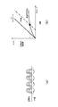
- FIG. 1 is a diagram for explaining surface plasmons.
- a plasmon (plasma wave) in a metal has a surface mode that interacts with light near the surface, and is called a surface plasmon.
- FIG. 1A is a conceptual diagram of surface plasmons. Near the surface, there is an electric field component in the surface normal direction due to the electron dense wave, and surface plasmon can be excited by using p-polarized incident light having an electric field component in the surface normal direction. It is known that It is also known that surface plasmons exhibit a dispersion relationship different from that of light propagating in free space.
- the dispersion relationship can be expressed as equation (1) using the surface plasmon wave number kx at the interface, the dielectric constant ⁇ 1 of the metal medium, and the dielectric constant ⁇ 2 of the peripheral medium.
- ⁇ is the angular frequency
- c is the speed of light in vacuum.
- (B) in FIG. 1 shows the dispersion relation of surface plasmons.
- the dispersion curve of the surface plasmon on the flat metal surface is always on the right side of the light line LL and does not have an intersection with the light line LL. That is, surface plasmons cannot be excited by light propagating in free space. Therefore, for example, a diffraction grating is used to excite surface plasmons.
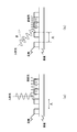
- FIG. 2 shows the optical arrangement of surface plasmon excitation.
- the wave number kx of the diffracted light is represented by the formula (2).
- K0 is the wave number of the propagating light
- m is the diffraction order, which is an integer.
- K is a lattice vector.
- kx k0 ⁇ Sin ⁇ + mK (2)
- ⁇ is the period of the diffraction grating. Therefore, by adjusting the incident angle ⁇ of the light and the period ⁇ of the diffraction grating, the dispersion curves of the diffracted light and the surface plasmon are made coincident so that energy transfer, that is, excitation light (transmitted light) can be generated.
- the wave number shift increases as the incident angle ⁇ increases, and the wavelength of the excitation light (transmitted light) generated by energy transfer (excitation wavelength, transmission wavelength). ) Shifts to shorter wavelengths. Therefore, in order to excite (transmit) the same wavelength, the period ⁇ of the diffraction grating is increased in accordance with the incident angle.
- the incident light to be excited is p-polarized light parallel to the periodic structure (periodic direction).
- the metal used for the diffraction grating has a wider wavelength selection (surface plasmon) range as the plasma frequency is higher.
- the plasma vibration is a longitudinal wave, and light having a frequency equal to or lower than the plasma frequency is totally reflected on the metal surface.
- the plasma frequency ⁇ p can be converted into the wavelength ⁇ based on the equation (3).
- ⁇ 2 ⁇ c / ⁇ p (3)
- the visible light wavelength ⁇ v can be converted into the angular frequency ⁇ based on the equation (4).
- ⁇ 2 ⁇ c / ⁇ v (4)
- Equation (5) 1 ⁇ ( ⁇ p 2 / ⁇ 2 ) (5)
- the period ⁇ of the periodic structure necessary for excitation can be calculated based on the equation (6).
- the dielectric constant ⁇ 2 is a dielectric constant ⁇ ( ⁇ ) calculated based on the equation (5).
- M is an integer
- k is a wave vector
- ⁇ is an incident angle.
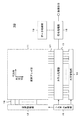
- FIG. 3 shows a schematic configuration of a solid-state imaging device to which the present technology is applied, for example, an XY address type CMOS image sensor.
- the CMOS image sensor is an image sensor created by applying or partially using a CMOS process.
- the CMOS image sensor 10 includes a pixel array unit 11 formed on a semiconductor substrate (chip) (not shown) and a peripheral circuit unit integrated on the same semiconductor substrate as the pixel array unit 11.
- the peripheral circuit unit includes, for example, a vertical drive unit 12, a column processing unit 13, a horizontal drive unit 14, and a system control unit 15.
- the CMOS image sensor 10 includes a signal processing unit 18 and a data storage unit 19.
- the signal processing unit 18 and the data storage unit 19 may be mounted on the same substrate as the CMOS image sensor 10 or may be disposed on a different substrate from the MOS image sensor 10.
- each processing of the signal processing unit 18 and the data storage unit 19 may be processing by an external signal processing unit or software provided on a substrate different from the CMOS image sensor 10.
- the pixel array unit 11 has a configuration in which a plurality of unit pixels are arranged in the row direction and the column direction.
- the row direction is the pixel arrangement direction (for example, horizontal direction) of the pixel row
- the column direction is the pixel arrangement direction (for example, vertical direction) of the pixel column.
- the arrangement direction of the metal wires is a direction in which desired polarization information is obtained
- the arrangement period of the metal wires (corresponding to the period of the diffraction grating) is a period for transmitting light of a desired wavelength from incident light.
- An optical element such as a wire grid polarizer is provided on an incident surface described later, and is configured to have a polarization pixel. Details of the polarization pixel will be described later.
- the pixel array unit 11 unit pixel includes a photoelectric conversion unit (for example, a photodiode) that generates and accumulates charges according to the received light amount, and a plurality of pixel transistors.
- the plurality of pixel transistors can be constituted by three transistors, for example, a transfer transistor, a reset transistor, and an amplification transistor.
- the plurality of pixel transistors can be configured by four transistors by further adding a selection transistor. Since the equivalent circuit of each pixel is the same as a general circuit, detailed description is omitted here.
- pixel drive lines 16 as row signal lines are wired along the row direction for each pixel row, and vertical signal lines 17 as column signal lines are wired along the column direction for each pixel column. Yes.
- the pixel drive line 16 transmits a drive signal for driving when reading a signal from the pixel.
- the pixel drive line 16 is shown as one wiring, but is not limited to one.
- One end of the pixel drive line 16 is connected to an output end corresponding to each row of the vertical drive unit 12.
- the vertical drive unit 12 is configured by a shift register, an address decoder, and the like, and drives each pixel of the pixel array unit 11 at the same time or in units of rows. That is, the vertical drive unit 12 constitutes a drive unit that controls the operation of each pixel of the pixel array unit 11 together with the system control unit 15 that controls the vertical drive unit 12.
- the vertical drive unit 12 is not shown in the figure for its specific configuration, but generally has a configuration having two scanning systems, a reading scanning system and a sweeping scanning system.
- the readout scanning system selectively scans the unit pixels of the pixel array unit 11 in units of rows in order to read out signals from the unit pixels.
- the signal read from the unit pixel is an analog signal.
- the sweep-out scanning system performs sweep-out scanning on the readout line on which readout scanning is performed by the readout scanning system prior to the readout scanning by the exposure time.
- the signal read out by the readout operation by the readout scanning system corresponds to the amount of light received after the immediately preceding readout operation or electronic shutter operation.
- a period from the read timing by the immediately preceding read operation or the sweep timing by the electronic shutter operation to the read timing by the current read operation is the charge exposure period in the unit pixel.
- a signal output from each unit pixel of the pixel row selectively scanned by the vertical driving unit 12 is input to the column processing unit 13 through each of the vertical signal lines 17 for each pixel column.
- the column processing unit 13 performs predetermined signal processing on signals output from the pixels in the selected row through the vertical signal line 17 for each pixel column of the pixel array unit 11, and temporarily outputs the pixel signals after the signal processing. Hold on.
- the column processing unit 13 performs noise removal processing, A / D (analog-digital) conversion, and the like as signal processing.
- the horizontal drive unit 14 includes a shift register, an address decoder, and the like, and sequentially selects unit circuits corresponding to the pixel columns of the column processing unit 13. By the selective scanning by the horizontal drive unit 14, pixel signals subjected to signal processing for each unit circuit in the column processing unit 13 are sequentially output.
- the system control unit 15 includes a timing generator that generates various timing signals, and the vertical driving unit 12, the column processing unit 13, and the horizontal driving unit 14 based on various timings generated by the timing generator. Drive control is performed.
- the signal processing unit 18 performs various signal processing on the pixel signal output from the column processing unit 13.
- the pixel array unit 11 can acquire polarization information for each color component, as will be described later. Therefore, the signal processing unit 18 acquires polarization characteristic information as described later based on the polarization information for each color component.
- the signal processing unit 18 performs separation and extraction of the reflection component based on the polarization characteristic information by using, for example, a technique disclosed in a patent document (International Publication No. 2016/136085). Further, the signal processing unit 18 may perform subject recognition, orientation / posture determination, and the like using, for example, a technique disclosed in a patent document (International Publication No. 2016/174915).
- the data storage unit 19 temporarily stores data necessary for the signal processing in the signal processing unit 18.
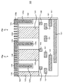
- FIG. 4 is a cross-sectional view schematically showing a configuration example of a CMOS image sensor.
- FIG. 4 shows a cross section of the polarizing pixel portion.
- the light incident side (upper side in FIG. 4) is above the CMOS image sensor 10, and the opposite side (lower side in FIG. 4) is below the CMOS image sensor 10.
- the CMOS image sensor 10 has a so-called back-illuminated structure in which light enters from the back side opposite to the surface on which the wiring layer 101 of the semiconductor substrate 102 is laminated.
- the back surface of the semiconductor substrate 102 is referred to as an incident surface or an imaging surface.
- wiring 121 is laminated over a plurality of layers.
- a gate electrode 122 is formed for each pixel in the vicinity of the boundary between the wiring layer 101 and the semiconductor substrate 102.
- a photoelectric conversion element 123 is formed in the region of the polarization pixel.
- the photoelectric conversion element 123 is configured by, for example, a photodiode.
- a trench is formed between the photoelectric conversion elements 123 from the incident surface side of the semiconductor substrate 102.
- An insulating film 124 is formed on the incident surface of the semiconductor substrate 102 and the wall surface of the trench.
- a vertical portion 125 a of the light shielding film 125 is embedded in the trench of the semiconductor substrate 102.
- the horizontal portion 125 b of the light shielding film 125 and the polarizer 126 are formed via the insulating film 124.
- the horizontal portion 125 b of the light shielding film 125 covers the incident surface of the semiconductor substrate 102, and an opening is formed above the photoelectric conversion element 123. That is, the horizontal portion 125b of the light shielding film 125 is formed so as to fill in between adjacent pixels. Incidence of light in an oblique direction from adjacent pixels is suppressed by the vertical portion 125a and the horizontal portion 125b of the light shielding film 125.
- the polarizer 126 is formed in the opening above the photoelectric conversion element 123 in the horizontal portion 125 b of the light shielding film 125 and covers the upper surface (incident surface) of the photoelectric conversion element 123.
- the polarizer 126 is, for example, a wire grid polarizer.
- the polarizer 126 passes a polarized wave having an electric field component perpendicular to the direction in which the wire grid extends, and suppresses the passage of a polarized wave having an electric field component parallel to the direction in which the wire grid extends.
- As a material of the polarizer 126 for example, aluminum, copper, gold, silver, platinum, tungsten, or an alloy containing these metals is used.
- the polarizer 126 has a configuration in which a wire grid is provided in a direction in which desired polarization information can be obtained, and the arrangement period of the wire grid is set according to the transmitted color and the incident angle of incident light as described later. ing.
- the pixel array unit 11 is configured using polarized pixels or polarized images and non-polarized pixels.
- the arrangement direction of the wire grid is a direction in which desired polarization information can be obtained.
- the arrangement period of the wire grid is a period for transmitting (exciting) light having a desired wavelength from incident light. As described above, this wire grid is provided above the photoelectric conversion element 123, that is, on the incident surface of the CMOS image sensor.
- the wire grid array direction and array cycle are set in units of pixels. Further, for example, in the pixel block composed of a plurality of pixels, the polarization pixels are arranged in different directions from each other in the wire grid arrangement direction of each pixel. Therefore, a plurality of pieces of polarization information having different polarization directions can be acquired for each pixel block.
- the arrangement direction of the wire grid is set so that the polarization characteristic information can be acquired using the pixel values of the polarization pixels of different arrangement directions.
- the polarization angle ⁇ pol when the maximum luminance Idmax is observed is the azimuth angle ⁇ d
- a predetermined change caused by a change in the luminance Idpol observed when the polarization angle is rotated that is, a difference in the polarization angle.
- the polarization model equation showing the luminance change can be expressed as equation (7).
- Equation (7) the polarization angle ⁇ pol is obvious when the polarization image is generated, and the maximum luminance Idmax, the minimum luminance Idmin, and the azimuth angle ⁇ d are variables. Accordingly, since there are three variables, the normal vector information generation unit 35 performs fitting to the function shown in Expression (7) using the luminance of the polarization image having three or more polarization directions, and the luminance and the polarization angle. The polarization characteristic information indicating the relationship can be acquired.
- the wire grid array period in each pixel is set to an equal period. Therefore, it becomes possible to acquire the polarization characteristic information for the color component corresponding to the array period of the wire grid for each pixel block.
- FIG. 5 exemplifies the pixel arrangement of the pixel array unit.
- the peripheral pixel block BPb incident light is incident.
- the angle ⁇ b is “ ⁇ b> 0 degree”.
- FIG. 6 illustrates the configuration of the pixel block BPa.
- the pixel block of 2 ⁇ 2 pixels has any one of four directions in which the arrangement direction of the wire grids is different and is different from each other.
- the arrangement period of the wire grid is an arrangement period ⁇ a .
- FIG. 6 shows the case where the wire grid has a horizontal direction and a tilt of 135 °, but the arrangement period is the same when the wire grid has a vertical direction and a tilt of 45 °.
- FIG. 7 illustrates the pixel block BPa in the central portion and the pixel block BPb in the peripheral portion.
- FIG. 7A shows the configuration of the pixel block BPa in the central portion.
- the wire grid has an arrangement period ⁇ ⁇ a in the pixel block of 2 ⁇ 2 pixels.
- FIG. 7B shows the configuration of the pixel block BPb in the peripheral portion.
- the transmission (excitation) wavelength shifts to a short wavelength when the incident angle increases. Therefore, in order to transmit (excite) the same wavelength as the pixel block BPa in the central portion, the wire grid is set to an arrangement period ⁇ ⁇ b (> ⁇ ⁇ a ) corresponding to the incident angle. As described above, when the arrangement period is set in accordance with the incident angle, polarization information having the same wavelength can be acquired not only in the central portion but also in the peripheral portion of the pixel array portion.
- a 2 ⁇ 2 pixel block is set as a color array unit (4 ⁇ 4 pixels), and four pixel blocks are set as a red unit, a blue unit, and two green units.
- FIG. 8 illustrates the pixel block BPa at the center when the pixel array portion is a Bayer array.
- the arrangement period of the wire grid is set to an arrangement period ⁇ r ⁇ a so that the red wavelength is transmitted (excited).
- the arrangement period of the wire grid is set to an arrangement period ⁇ g ⁇ a so that the green wavelength is transmitted (excited).
- the arrangement period of the wire grid is set to the arrangement period ⁇ b ⁇ a so that the blue wavelength is transmitted (excited).
- polarization characteristic information can be acquired for each color component without using a color filter.
- polarization characteristic information can be acquired for each color component not only in the central part but also in the peripheral part of the pixel array part.
- polarization information can be acquired for each color component by using a wire grid having a thickness of 100 to several hundred nm without using a color filter having a thickness of several hundred to several hundreds of nm.
- a low profile structure can be realized as compared with a CMOS image sensor in which a color filter is provided in the sensor.
- the low-profile structure makes it possible to reduce the amount of pupil correction and realize a narrow band of a desired signal, and to secure various manufacturing margins and characteristic margins.
- the basic unit may be two directions of 0 degree and 90 degrees, or two directions of 45 degrees and 135 degrees. Further, for example, 22.5 degrees, 67.5 degrees, 112.5 degrees, 157.5 degrees, and the like may be added to the polarization direction to increase the basic unit from four directions. In this case, polarization information can be acquired with high accuracy.
- polarization information for each color component may be acquired by using a plurality of CMOS image sensors each having a pixel array having the configuration shown in FIGS.
- the arrangement period of the wire grid in the central portion of the pixel array is set to the arrangement period ⁇ r ⁇ a so that the red wavelength is transmitted (excited).
- the arrangement period of the wire grid in the peripheral portion is an arrangement period corresponding to the incident angle, for example, an arrangement period ⁇ r ⁇ b when the incident angle is ⁇ b.
- the arrangement period of the wire grid in the center portion of the pixel array is set to an arrangement period ⁇ g ⁇ a so as to transmit (excite) the green wavelength.
- the arrangement period of the wire grid in the peripheral portion is an arrangement period corresponding to the incident angle, for example, an arrangement period ⁇ g ⁇ b when the incident angle is ⁇ b.
- the arrangement period of the wire grid in the central portion of the pixel array is set to the arrangement period ⁇ b ⁇ a so that the blue wavelength is transmitted (excited).
- the arrangement period of the wire grid in the peripheral portion is an arrangement period corresponding to the incident angle, for example, an arrangement period ⁇ b ⁇ b when the incident angle is ⁇ b.
- FIG. 9 exemplifies a configuration in the case of acquiring polarization information for each color component using a plurality of CMOS image sensors.
- Incident light is divided into, for example, three by the light dividing unit 20.
- the divided light is input to the CMOS image sensor 10R that acquires the polarization information of the red component, the CMOS image sensor 10G that acquires the polarization information of the green component, and the CMOS image sensor 10B that acquires the polarization information of the blue component.
- the CMOS image sensor 10R the polarization information of the red component is generated as described above.
- the CMOS image sensor 10G generates green component polarization information as described above.
- the CMOS image sensor 10B generates blue component polarization information as described above. Therefore, polarization information for each desired color component can be generated without using a color separation prism or the like. Further, by providing a CMOS image sensor for each color component, it is possible to obtain detailed polarization information while maintaining the resolution.
- CMOS image sensors when a color separation prism is used instead of the light splitting unit 20 as in the past, if the arrangement period of the wire grid is adjusted according to the wavelength of the color separation light, light of a desired wavelength can be transmitted accurately ( Excitation). Furthermore, if four or more CMOS image sensors are provided, detailed polarization information can be acquired for each more detailed color component while maintaining the resolution.
- CMOS image sensor has the configuration shown in FIG. 4, the incident angle becomes large in the peripheral pixels, so that it is difficult for light to enter the photoelectric conversion element 123. Therefore, in another configuration of the solid-state imaging device shown in FIG. 10, a condensing element 127, for example, an on-chip lens is formed above the wire grid (on the side opposite to the incident surface). As described above, when the light collecting element 127 is provided, incident light can be efficiently incident on the photoelectric conversion element 123.
- the on-chip lens may be provided for each pixel, for example, or may be provided for each pixel block that is greatly omitted by a plurality of polarization pixels having different polarization directions.
- FIG. 10 illustrates the case where each pixel is provided.
- FIG. 11 shows a case where the position of the on-chip lens with respect to the pixel or the pixel block is moved according to the incident angle.
- the position of the on-chip lens with respect to the pixel or the pixel block is adjusted according to the incident angle, and as the incident angle increases, the optical axis position LPc of the on-chip lens is changed, for example, from the center position GPc of the pixel. Move more in the direction.
- incident light can be efficiently incident on the photoelectric conversion element 123 via the polarizer 126, compared to the case where the center position of the on-chip lens is the center position of the pixel.
- incident light may be incident on the CMOS image sensor 10 via an aspheric lens (or a lens group configured using a plurality of lenses).
- an aspheric lens or a lens group configured using a plurality of lenses.
- the relationship between the incident light incident on the aspherical lens and the image height has nonlinear characteristics. Therefore, when the incident light incident on the CMOS image sensor 10 is incident through the aspheric lens, the arrangement period is adjusted according to the incident angle of the incident light through the aspheric lens.
- the arrangement direction and the arrangement period of the wire grid polarizer may be set so that polarization information of a desired color component can be obtained and provided on the incident surface of the image sensor.
- the configuration is not limited to those shown in FIGS. 4, 10, and 11.
- the image sensor is not limited to a CMOS image sensor, and may be an image sensor of another type (for example, a CCD image sensor).
- the filling material is silicon dioxide, and the dielectric constant is 2.25.
- the wavelength of the red component is “2898 THz” when an angular frequency is set based on the equation (4).
- the plasma frequency of aluminum is “24000 THz”.
- the arrangement period ⁇ r ⁇ b is “549.173 nm” based on the equation (2) and the like.
- the plasma frequency of aluminum is “24000 THz”.
- the arrangement period ⁇ g ⁇ b is “460.501 nm” based on the equation (2) and the like.
- the solid-state imaging device of the present technology can also have the following configuration.
- An optical element in which the arrangement direction of the metal wires is a direction in which desired polarization information is obtained, and the arrangement period of the metal wires is a period for transmitting light of a desired wavelength from incident light is defined as an incident surface of the imaging element.
- Solid-state imaging device provided in (2) The solid-state imaging device according to (1), wherein the optical element is a wire grid polarizer.
- the solid-state imaging device according to (2), wherein the arrangement direction of the wire grid and the arrangement period are set in units of pixels.
- the solid-state imaging device according to (3), wherein the arrangement direction of the wire grid in each pixel is different from each other in a pixel block including a plurality of pixels.
- the solid-state imaging device In the pixel block including the plurality of pixels, the solid-state imaging device according to (4), wherein the array period of the wire grid in each pixel is set to an equal period.
- the solid-state imaging device (7) The solid-state imaging device according to (6), wherein the position of the lens with respect to the pixel or the pixel block is moved in the direction of the incident light according to an incident angle of the incident light.
- an electronic device having the following configuration can be provided.
- the arrangement direction of the metal wires is a direction in which desired polarization information can be obtained, and the arrangement period of the metal wires is desired from incident light.
- a solid-state imaging device in which an optical element having a period for transmitting light of the wavelength is provided on the incident surface of the imaging element;
- An electronic apparatus comprising: a signal processing unit that performs signal processing using polarization information of a desired wavelength obtained by the solid-state imaging device.
- the arrangement direction of the metal wires is a direction in which desired polarization information is obtained
- the arrangement period of the metal wires is a period in which light having a desired wavelength is transmitted from incident light.
- the element is provided on the incident surface of the imaging element. Therefore, polarization information can be easily acquired for each color component.
- polarization information is used for each color component, various signal processes such as removal of reflection components and detection of the orientation and orientation of a subject can be performed, which is suitable for a monitoring system, a mobile control system, and the like.
Landscapes
- Physics & Mathematics (AREA)
- Engineering & Computer Science (AREA)
- Multimedia (AREA)
- Signal Processing (AREA)
- General Physics & Mathematics (AREA)
- Optics & Photonics (AREA)
- Polarising Elements (AREA)
- Solid State Image Pick-Up Elements (AREA)
- Transforming Light Signals Into Electric Signals (AREA)
- Color Television Image Signal Generators (AREA)
- Studio Devices (AREA)
- Optical Filters (AREA)
Abstract
光学素子としてワイヤーグリッド偏光子を撮像素子の入射面に設ける。ワイヤーグリッドの配列方向は所望の偏光情報が得られる方向で、配列周期は入射光から所望の波長の光を透過する周期とする。配列方向と配列周期は画素単位で設定する。例えば、2×2画素の画素ブロックでは、各画素の配列方向は、互いに異なる4つの偏光方向とする。また、画素ブロックでは、各画素における配列周期が等しい周期とする。例えば赤色成分の偏光情報を取得する赤色単位UPrの画素ブロックは赤色成分に応じた配列周期Λrθa、緑色成分の偏光情報を取得する緑色単位UPgの画素ブロックは緑色成分に応じた配列周期Λgθa、青色成分の偏光情報を取得する青色単位UPbの画素ブロックは青色成分に応じた配列周期Λbθaとする。また、入射光の入射角に応じて配列周期等を調整する。色成分毎に偏光情報を容易に取得できるようになる。
Description
この技術は、固体撮像装置に関し、色成分毎に偏光情報を得られるようにする。
従来、例えば特許文献1では、受光素子(光電変換層)に光共鳴構造体を形成し、局在プラズモン共鳴または導波モード共鳴の性質を利用して色分解を行うことが記載されている。また、非特許文献1では、可視領域の波長を励起可能な程度の周期構造を有するAlナノワイヤーアレイを用いて、可視域プラスモニックフィルタを構成することが記載されている。
本間浩章「MEMS技術を用いた表面プラズモンの異常透過制御技術の研究」豊橋技術科学大学 学位授与番号 甲第741号 2016-03-23、インターネット(URL:http://id.nii.ac.jp/1117/00001948/)
ところで、多波長分光特性を有するためには、特許文献1や非特許文献1のように、表面プラズモン特性を利用することが一般的である。しかし、特許文献1や非特許文献1の技術では、被写体の偏光特性を示す偏光情報を取得することができない。
そこで、この技術では、色成分毎に偏光情報を容易に取得できる固体撮像装置を提供することを目的とする。
この技術の第1の側面は、
金属ワイヤーの配列方向が所望の偏光情報が得られる方向であり、前記金属ワイヤーの配列周期が入射光から所望の波長の光を透過する周期である光学素子を、撮像素子の入射面に設けた
固体撮像装置にある。
金属ワイヤーの配列方向が所望の偏光情報が得られる方向であり、前記金属ワイヤーの配列周期が入射光から所望の波長の光を透過する周期である光学素子を、撮像素子の入射面に設けた
固体撮像装置にある。
この技術においては、光学素子としてワイヤーグリッド偏光子を撮像素子の入射面に設ける。ワイヤーグリッドの配列方向は所望の偏光情報が得られる方向であり、配列周期は入射光から所望の波長の光を透過する周期とされている。また、ワイヤーグリッドの配列方向と配列周期は画素単位で設定されている。例えば、複数画素からなる画素ブロックにおいて、各画素におけるワイヤーグリッドの配列方向が互いに異なる方向とされている。また、複数画素からなる画素ブロックでは、各画素におけるワイヤーグリッドの配列周期が等しい周期とされている。
また、画素毎または画素ブロック毎にレンズを設けて、入射光をレンズとワイヤーグリッドを介して入射面に入射させる。また、入射光の入射角に応じて、画素または画素ブロックに対するレンズの位置を入射光の方向へ移動する。さらに、入射光の入射角に応じて配列周期を調整して、所望の波長の光を透過させる。
また、非球面レンズを介して入射光が入射される場合、非球面レンズを介した入射光の入射角に応じて配列周期を調整する。
この技術によれば、金属ワイヤーの配列方向が所望の偏光情報が得られる方向であり、前記金属ワイヤーの配列周期が入射光から所望の波長の光を透過する周期である光学素子が、撮像素子の入射面に設けられる。このため、色成分毎に偏光情報を容易に取得できるようになる。なお、本明細書に記載された効果はあくまで例示であって限定されるものではなく、また付加的な効果があってもよい。
以下、本技術を実施するための形態について説明する。なお、説明は以下の順序で行う。
1.プラズモン励起に必要な周期構造について
2.固体撮像装置の構成について
3.固体撮像装置の他の構成について、
4.具体例
1.プラズモン励起に必要な周期構造について
2.固体撮像装置の構成について
3.固体撮像装置の他の構成について、
4.具体例
<1.プラズモン励起に必要な周期構造について>
表面プラズモンは、金属の表面100nm近傍の領域に存在するプラズマ電子による縦波であり、これらがある条件下で励起すなわちエネルギーの授受が行われる。
表面プラズモンは、金属の表面100nm近傍の領域に存在するプラズマ電子による縦波であり、これらがある条件下で励起すなわちエネルギーの授受が行われる。
図1は、表面プラズモンを説明するための図である。金属中のプラズモン(プラズマ波)は、表面近傍で光と相互作用する表面モードが存在しており、表面プラズモンと呼ばれている。図1の(a)は、表面プラズモンの概念図である。表面近傍では,電子の粗密波に起因した面法線方向の電場成分が存在しており、面法線方向の電場成分を有するp偏光の入射光を用いることで表面プラズモンを励起することが可能であることが知られている。また、表面プラズモンが自由空間中を伝搬する光とは異なる分散関係を示すことが知られている。分散関係は、界面における表面プラズモンの波数kx、金属媒質の誘電率ε1と周辺媒質の誘電率ε2を用いて、式(1)として表すことができる。ここで、「ω」は角振動数、「c」は真空中の光速である。

図1の(b)は表面プラズモンの分散関係を示している。ここで、入射光(k=ω/c)を示すライトラインLLの左側の領域にあれば,光による励起が可能である。しかし、平坦な金属表面での表面プラズモンの分散曲線は常にライトラインLLの右側にありライトラインLLとの交点を持たない。すなわち,自由空間を伝搬する光では表面プラズモンを励起できない。そこで、表面プラズモンを励起するために例えば回折格子を用いる。
図2は、表面プラズモン励起の光学配置を示している。回折光の波数kxは、式(2)の関係となる。なお、「k0」は伝搬光の持つ波数、「m」は回折次数であり整数である。「K」は格子ベクトルである。
kx=k0・Sinθ+mK ・・・(2)
kx=k0・Sinθ+mK ・・・(2)
また、光が回折格子に入射すると分散曲線は格子ベクトルK=2π/Λの整数倍だけシフトして、回折光と表面プラズモンの分散曲線の交わる点が生じる。なお、「Λ」は回折格子の周期である。したがって、光の入射角θや回折格子の周期Λを調整して、回折光と表面プラズモンの分散曲線を一致させて、エネルギー授受すなわち励起光(透過光)を生成できるようにする。
さらに、光の入射角θが「0」である場合に比べて、入射角θが大きくなると、波数のシフトが大きくなり、エネルギー授受によって生じる励起光(透過光)の波長(励起波長,透過波長)は短波長にシフトする。したがって、同一波長を励起(透過)するために、入射角に応じて回折格子の周期Λを広げるようにする。
次に、回折格子の周期構造について説明する。励起される入射光は周期構造(周期方向)に対して平行なp偏光である。回折格子に用いる金属は、プラズマ周波数が高いほど波長選択(表面プラズモン)範囲が広くなる。また、プラズマ振動は縦波であり、プラズマ周波数以下の周波数の光は金属表面で全反射される。ここで、プラズマ周波数ωpは、式(3)に基づき波長λに換算することができる。
λ = 2πc/ωp ・・・(3)
λ = 2πc/ωp ・・・(3)
また、式(4)に基づき可視光波長λvを角周波数ωに変換できる。
ω = 2πc/λv ・・・(4)
ω = 2πc/λv ・・・(4)
さらに、回折格子に用いる金属の誘電率の周波数依存性は、無損失ドルーデモデルである式(5)に基づき算出できる。
ε(ω) = 1-(ωp 2/ω2) ・・・(5)
ε(ω) = 1-(ωp 2/ω2) ・・・(5)
また、埋め込み材の誘電率ε1とすると、励起に必要な周期構造の周期Λは式(6)に基づき算出できる。なお、誘電率ε2は、式(5)に基づいて算出された誘電率ε(ω)である。「m」は整数,「k」は波数ベクトル、「θ」は入射角である。

<2.固体撮像装置の構成について>
図3は、本技術が適用される固体撮像装置、例えばX-Yアドレス方式のCMOSイメージセンサの概略構成を示している。ここで、CMOSイメージセンサとは、CMOSプロセスを応用して、または、部分的に使用して作成されたイメージセンサである。
図3は、本技術が適用される固体撮像装置、例えばX-Yアドレス方式のCMOSイメージセンサの概略構成を示している。ここで、CMOSイメージセンサとは、CMOSプロセスを応用して、または、部分的に使用して作成されたイメージセンサである。
CMOSイメージセンサ10は、図示せぬ半導体基板(チップ)上に形成された画素アレイ部11と、画素アレイ部11と同じ半導体基板上に集積された周辺回路部とを有する構成となっている。周辺回路部は、例えば、垂直駆動部12、カラム処理部13、水平駆動部14及びシステム制御部15から構成されている。
また、CMOSイメージセンサ10は、信号処理部18及びデータ格納部19を備えている。信号処理部18及びデータ格納部19については、CMOSイメージセンサ10と同じ基板上に搭載しても構わないし、本MOSイメージセンサ10と別の基板上に配置するようにしても構わない。また、信号処理部18及びデータ格納部19の各処理については、CMOSイメージセンサ10とは別の基板に設けられる外部信号処理部やソフトウェアによる処理でも構わない。
画素アレイ部11は、複数の単位画素が行方向及び列方向に配置された構成となっている。ここで、行方向とは画素行の画素の配列方向(例えば水平方向)であり、列方向とは画素列の画素の配列方向(例えば垂直方向)とする。
画素アレイ部11には、金属ワイヤーの配列方向を所望の偏光情報が得られる方向として、金属ワイヤーの配列周期(回折格子の周期に相当)を入射光から所望の波長の光を透過する周期とした光学素子、例えばワイヤーグリッド偏光子が後述する入射面に設けられて、偏光画素を有するように構成されている。なお、偏光画素の詳細については後述する。
画素アレイ部11単位画素は、受光した光量に応じた電荷を生成しかつ蓄積する光電変換部(例えば、フォトダイオード)、及び、複数の画素トランジスタを有する。複数の画素トランジスタは、例えば、転送トランジスタ、リセットトランジスタ、および増幅トランジスタの3つのトランジスタで構成することができる。あるいは、複数の画素トランジスタは、さらに選択トランジスタを追加して4つのトランジスタで構成することもできる。なお、各画素の等価回路は一般的なものと同様であるので、ここでは詳細な説明は省略する。
画素アレイ部11において、画素行毎に行信号線としての画素駆動線16が行方向に沿って配線され、画素列毎に列信号線としての垂直信号線17が列方向に沿って配線されている。画素駆動線16は、画素から信号を読み出す際の駆動を行うための駆動信号を伝送する。図3では、画素駆動線16について1本の配線として示しているが、1本に限られるものではない。画素駆動線16の一端は、垂直駆動部12の各行に対応した出力端に接続されている。
垂直駆動部12は、シフトレジスタやアドレスデコーダなどによって構成され、画素アレイ部11の各画素を全画素同時あるいは行単位等で駆動する。すなわち、垂直駆動部12は、垂直駆動部12を制御するシステム制御部15と共に、画素アレイ部11の各画素の動作を制御する駆動部を構成している。この垂直駆動部12はその具体的な構成については図示を省略するが、一般的に、読出し走査系と掃出し走査系の2つの走査系を有する構成となっている。
読出し走査系は、単位画素から信号を読み出すために、画素アレイ部11の単位画素を行単位で順に選択走査する。単位画素から読み出される信号はアナログ信号である。掃出し走査系は、読出し走査系によって読出し走査が行われる読出し行に対して、その読出し走査よりも露光時間分だけ先行して掃出し走査を行う。
この掃出し走査系による掃出し走査により、読出し行の単位画素の光電変換部から不要な電荷が掃き出されることによって当該光電変換部がリセットされる。そして、この掃出し走査系による不要電荷の掃き出す(リセットする)ことにより、いわゆる電子シャッタ動作が行われる。
読出し走査系による読出し動作によって読み出される信号は、その直前の読出し動作または電子シャッタ動作以降に受光した光量に対応するものである。そして、直前の読出し動作による読出しタイミングまたは電子シャッタ動作による掃出しタイミングから、今回の読出し動作による読出しタイミングまでの期間が、単位画素における電荷の露光期間となる。
垂直駆動部12によって選択走査された画素行の各単位画素から出力される信号は、画素列毎に垂直信号線17の各々を通してカラム処理部13に入力される。カラム処理部13は、画素アレイ部11の画素列毎に、選択行の各画素から垂直信号線17を通して出力される信号に対して所定の信号処理を行うとともに、信号処理後の画素信号を一時的に保持する。例えば、カラム処理部13は、信号処理として、ノイズ除去処理やA/D(アナログ-デジタル)変換等を行う。
水平駆動部14は、シフトレジスタやアドレスデコーダなどによって構成され、カラム処理部13の画素列に対応する単位回路を順番に選択する。この水平駆動部14による選択走査により、カラム処理部13において単位回路毎に信号処理された画素信号が順番に出力される。
システム制御部15は、各種のタイミング信号を生成するタイミングジェネレータなどによって構成され、当該タイミングジェネレータで生成された各種のタイミングを基に、垂直駆動部12、カラム処理部13、及び、水平駆動部14などの駆動制御を行う。
信号処理部18は、カラム処理部13から出力される画素信号に対して種々の信号処理を行う。画素アレイ部11では、後述するように色成分毎の偏光情報を取得できる。したがって、信号処理部18は、色成分毎の偏光情報に基づき、後述するように偏光特性情報を取得する。また、信号処理部18は、例えば特許文献(国際公開第2016/136085号)の技術を用いることで、偏光特性情報に基づき反射成分の分離や抽出等を行う。さらに、信号処理部18は、例えば特許文献(国際公開第2016/174915号)の技術を用いることで、被写体の認識や向き・姿勢の判別等を行ってもよい。
データ格納部19は、信号処理部18での信号処理に当たって、その処理に必要なデータを一時的に格納する。
図4は、CMOSイメージセンサの構成例を模式的に示す断面図である。なお、図4では、偏光画素の部分の断面を示している。
なお、以下、光の入射側(図4の上側)をCMOSイメージセンサ10の上方とし、光の入射側と反対側(図4の下側)をCMOSイメージセンサ10の下方とする。
CMOSイメージセンサ10は、半導体基板102の配線層101が積層されている表面とは逆の裏面側から光が入射する、いわゆる裏面照射型の構造を有している。なお、以下、半導体基板102の裏面を入射面あるいは撮像面と称する。
配線層101には、配線121が複数の層にわたって積層されている。また、配線層101の半導体基板102との境界付近に、各画素に対してゲート電極122が形成されている。
半導体基板102には、偏光画素の領域内に光電変換素子123が形成されている。なお、光電変換素子123は、例えばフォトダイオードにより構成される。
各光電変換素子123間には、半導体基板102の入射面側からトレンチが形成されている。半導体基板102の入射面及びトレンチの壁面には絶縁膜124が形成されている。また、半導体基板102のトレンチ内には、遮光膜125の垂直部125aが埋め込まれている。
半導体基板102の入射面上には、絶縁膜124を介して、遮光膜125の水平部125b、偏光子126が形成されている。
遮光膜125の水平部125bは、半導体基板102の入射面を覆うとともに、光電変換素子123の上方に開口部が形成されている。すなわち、遮光膜125の水平部125bは、隣接する画素の間を埋めるように形成されている。この遮光膜125の垂直部125a及び水平部125bにより、隣接する画素からの斜め方向の光の入射が抑制される。
偏光子126は、遮光膜125の水平部125bの光電変換素子123の上方の開口部に形成され、光電変換素子123の上面(入射面)を覆っている。偏光子126は、例えばワイヤーグリッド偏光子である。偏光子126は、ワイヤーグリッドの延びる方向と直行する方向の電界成分を持つ偏光波を通過させ、ワイヤーグリッドの延びる方向と平行な電界成分を持つ偏光波の通過を抑制する。偏光子126の材料としては、例えば、アルミニウム、銅、金、銀、白金、タングステン、あるいは、これらの金属を含む合金等が用いられる。偏光子126では、ワイヤーグリッドを所望の偏光情報が得られる方向として設けた構成とされており、ワイヤーグリッドの配列周期は、後述するように透過する色および入射光の入射角に応じて設定されている。なお、図4および後述する図10,図11では、赤色画素PXrと赤色画素よりも波長の短い例えば緑色画素PXbを示している。
次に、画素アレイ部11について説明する。画素アレイ部11は偏光画素あるいは偏光画像と無偏光画素を用いて構成されている。偏光画素では、ワイヤーグリッドの配列方向を所望の偏光情報が得られる方向とする。また、偏光画素では、ワイヤーグリッドの配列周期を入射光から所望の波長の光を透過(励起)する周期とする。このワイヤーグリッドを、上述したように光電変換素子123の上方、すなわちCMOSイメージセンサの入射面に設ける。
ワイヤーグリッドの配列方向と配列周期は画素単位で設定されている。また、偏光画素は、例えば複数画素からなる画素ブロックにおいて、各画素のワイヤーグリッドの配列方向が互いに異なる方向とされている。したがって、画素ブロック毎に、偏光方向が異なる複数の偏光情報を取得できる。
また、ワイヤーグリッドの配列方向は、異なる配列方向の偏光画素の画素値を用いて偏光特性情報を取得できるように設定する。例えば、拡散反射の場合、最大輝度Idmaxが観測されたときの偏光角υpolを方位角φdとすると、偏光角を回転させたときに観測される輝度Idpolの変化、すなわち偏光角の違いによって生じる所定の輝度変化を示す偏光モデル式は、式(7)のように表すことができる。

式(7)では、偏光角υpolが偏光画像の生成時に明らかであり、最大輝度Idmaxと最小輝度Idminおよび方位角φdが変数となる。したがって、法線情報生成部35は、変数が3つであることから、偏光方向が3方向以上の偏光画像の輝度を用いて式(7)に示す関数へのフィッティングを行い、輝度と偏光角の関係を示す偏光特性情報を取得できる。
また、複数画素からなる画素ブロックでは、各画素におけるワイヤーグリッドの配列周期を等しい周期とする。したがって、画素ブロック毎に、ワイヤーグリッドの配列周期に対応する色成分についての偏光特性情報を取得できるようになる。
図5は、画素アレイ部の画素配置を例示しており、中央部分の画素ブロックBPaは、入射光の入射角θaが「θa=0度」、周辺部分の画素ブロックBPbでは、入射光の入射角θbが「θb>0度」となる。
図6は、画素ブロックBPaの構成を例示している。2×2画素の画素ブロックは、ワイヤーグリッドの配列方向が異なる4つの方向の何れかであって、互いに異なる配列方向とされている。また、2×2画素の画素ブロック内ではワイヤーグリッドの配列周期が配列周期Λθaとされている。なお、図6ではワイヤーグリッドが水平方向および135°の傾きを生じている場合を示しているが、ワイヤーグリッドが垂直方向および45°の傾きを生じている場合も配列周期は同様である。
図7は、中央部分の画素ブロックBPaと周辺部分の画素ブロックBPbを例示している。図7の(a)は、中央部分の画素ブロックBPaの構成を示しており、図6と同様に、2×2画素の画素ブロック内ではワイヤーグリッドが配列周期Λθaとされている。
図7の(b)は周辺部分の画素ブロックBPbの構成を示している。上述の「プラズモン励起に必要な周期構造について」で説明したように、入射角が大きくなると透過(励起)波長は短波長にシフトする。したがって、中央部分の画素ブロックBPaと同一波長を透過(励起)するために、ワイヤーグリッドを入射角に応じた配列周期Λθb(>Λθa)とする。このように、入射角に応じた配列周期とすれば、画素アレイ部の中央部だけでなく周辺部でも、同一波長の偏光情報を取得できるようになる。
また、画素アレイ部をベイヤー配列とする場合、2×2画素ブロックを色配列単位(4×4画素)として、4つの画素ブロックを赤色単位と青色単位と2つの緑色単位とする。図8は、画素アレイ部がベイヤー配列である場合の中央部分の画素ブロックBPaを例示している。
赤色単位UPrである2×2画素ブロック内ではワイヤーグリッドの配列周期が赤色の波長を透過(励起)するように配列周期Λrθaとされている。緑色単位UPgである2×2画素ブロック内ではワイヤーグリッドの配列周期が緑色の波長を透過(励起)するように配列周期Λgθaとされている。さらに、青色単位UPbである2×2画素ブロック内ではワイヤーグリッドの配列周期が青色の波長を透過(励起)するように配列周期Λbθaとされている。
このように、ワイヤーグリッドの配列周期を調整すれば、カラーフィルタを用いることなく、色成分毎に偏光特性情報を取得できるようになる。また、図示せずも、入射角に応じて各色の配列周期を調整すれば、画素アレイ部の中央部だけでなく周辺部でも、色成分毎に偏光特性情報を取得できるようになる。
また、本技術では、数百~千数百nmの厚さのカラーフィルタを用いることなく100~数百nmの厚さのワイヤーグリッドによって色成分毎に偏光情報を取得できる。このため、カラーフィルタをセンサ内に設けるCMOSイメージセンサに比べて、低背化構造を実現できる。また、低背化構造によって、瞳補正の補正量を少なくして所望の信号の狭帯域を実現することができ、各種製造上のマージンや特性上のマージンの確保が可能となる。
なお、図6乃至図8では、偏光方向が4方向である場合を示したが、偏光情報を粗にしても支障がない状況の場合(例えば凹凸のみを判別するような場合)、偏光方向を0度と90度の2方向、あるいは45度と135度の2方向を基本単位としてもよい。また、偏光方向に、例えば22.5度、67.5度、112.5度、157.5度等を追加して、基本単位を4方向よりも多くしてもよい。この場合、偏光情報を高精度に取得することが可能となる。
また、図6および図7に示す構成の画素アレイを有するCMOSイメージセンサを複数用いて、色成分毎の偏光情報を取得してもよい。例えば、赤色成分の偏光情報を取得するCMOSイメージセンサ10Rでは、画素アレイの中央部におけるワイヤーグリッドの配列周期は赤色の波長を透過(励起)するように配列周期Λrθaとする。また、周辺部におけるワイヤーグリッドの配列周期は、入射角に応じた配列周期として、例えば入射角θbのときは配列周期Λrθbとする。
同様に、緑色成分の偏光情報を取得するCMOSイメージセンサ10Gでは、画素アレイの中央部におけるワイヤーグリッドの配列周期は緑色の波長を透過(励起)するように配列周期Λgθaとする。また、周辺部におけるワイヤーグリッドの配列周期は、入射角に応じた配列周期として、例えば入射角θbのときは配列周期Λgθbとする。
さらに、青色成分の偏光情報を取得するCMOSイメージセンサ10Bでは、画素アレイの中央部におけるワイヤーグリッドの配列周期は青色の波長を透過(励起)するように配列周期Λbθaとする。また、周辺部におけるワイヤーグリッドの配列周期は、入射角に応じた配列周期として、例えば入射角θbのときは配列周期Λbθbとする。
図9は、CMOSイメージセンサを複数用いて色成分毎の偏光情報を取得する場合の構成を例示している。入射光は光分割部20で例えば3つに分割される。分割された光は、赤色成分の偏光情報を取得するCMOSイメージセンサ10Rと、緑色成分の偏光情報を取得するCMOSイメージセンサ10Gと、青色成分の偏光情報を取得するCMOSイメージセンサ10Bに入力される。CMOSイメージセンサ10Rでは、上述のように赤色成分の偏光情報を生成する。また、CMOSイメージセンサ10Gでは、上述のように緑色成分の偏光情報を生成する。さらに、CMOSイメージセンサ10Bでは、上述のように青色成分の偏光情報を生成する。したがって、色分解プリズム等を用いなくとも、所望の色成分毎の偏光情報を生成できるようになる。また、色成分毎にCMOSイメージセンサを設けることで、解像度を維持しつつ、詳細な偏光情報を得ることも可能である。
また、光分割部20に代えて従来のように色分解プリズムを用いた場合、色分解光の波長に対応させてワイヤーグリッドの配列周期を調整すれば、所望の波長の光を精度よく透過(励起)することも可能である。さらに、CMOSイメージセンサを4以上設けるようにすれば、解像度を維持しつつ、詳細な偏光情報をさらに詳細な色成分毎に取得することが可能となる。
<3.固体撮像装置の他の構成について>
CMOSイメージセンサが図4に示す構成である場合、周辺部の画素では入射角が大きくなるため、光電変換素子123に光が入射しにくい。そこで、図10に示す固体撮像装置の他の構成では、ワイヤーグリッドの上方(入射面面とは逆側)に、集光素子127例えばオンチップレンズを形成する。このように、集光素子127を設ければ、入射光を効率よく光電変換素子123に入射させることができる。
CMOSイメージセンサが図4に示す構成である場合、周辺部の画素では入射角が大きくなるため、光電変換素子123に光が入射しにくい。そこで、図10に示す固体撮像装置の他の構成では、ワイヤーグリッドの上方(入射面面とは逆側)に、集光素子127例えばオンチップレンズを形成する。このように、集光素子127を設ければ、入射光を効率よく光電変換素子123に入射させることができる。
オンチップレンズは、例えば画素毎に設けてもよく、偏光方向が異なる複数の偏光画素で猛省された画素ブロック毎に設けてもよい。なお、図10では画素毎に設けた場合を例示している。
さらに、入射光の入射角が大きくなる場合は、入射角に応じて、画素または画素ブロックに対するオンチップレンズの位置を入射光の方向へ移動してもよい。図11は、入射角に応じて画素や画素ブロックに対するオンチップレンズの位置を移動した場合を示している。このように、入射角に応じて画素や画素ブロックに対するオンチップレンズの位置を調整して、入射角が大きくなる伴い、オンチップレンズの光軸位置LPcを例えば画素の中心位置GPcから入射光の方向により多く移動させる。この場合、オンチップレンズの中心位置が画素の中心位置とされている場合に比べて、偏光子126を介して光電変換素子123に効率よく入射光を入射させることができる。
また、CMOSイメージセンサ10には、非球面レンズ(あるいは複数枚のレンズを用いて構成されたレンズ群)を介して入射光が入射される場合がある。ここで、非球面レンズに入射される入射光と像高の関係は非線形特性を有している。したがって、CMOSイメージセンサ10に入射される入射光が、非球面レンズを介して入射される場合は、非球面レンズを介した入射光の入射角に応じて配列周期を調整する。
なお、本技術は、ワイヤーグリッド偏光子の配列方向や配列周期を所望の色成分の偏光情報が得られるように設定して、イメージセンサの入射面に設ければよく、CMOSイメージセンサの構成は、図4や図10,図11に示す構成に限られない。また、CMOSイメージセンサに限らず他の方式のイメージセンサ(例えばCCDイメージセンサ)等であってもよい。
<4.具体例>
次に、偏光子126の材料として、例えばアルミニウムを用いた場合のワイヤーグリッドの配列周期について説明する。なお、埋め込み材は二酸化シリコンであり、誘電率は2.25とする。
次に、偏光子126の材料として、例えばアルミニウムを用いた場合のワイヤーグリッドの配列周期について説明する。なお、埋め込み材は二酸化シリコンであり、誘電率は2.25とする。
例えば赤色成分(λ=650nm)の偏光情報を取得する場合、赤色成分の波長を式(4)に基づき角周波数とすると「2898THz」となる。また、アルミニウムのプラズマ周波数は「24000THz」である。アルミニウムの誘電率の周波数依存性についてドルーデモデルを用いると、式(5)に基づき赤色成分の波長(λ=650nm)におけるアルミニウムの誘電率は「-67.56」となる。従って、式(6)に基づき、入射角θa(=0度)の配列周期Λrθaは「426.057nm」となる。また、入射角θb(=20度)である場合、式(2)等に基づき、配列周期Λrθbは「549.173nm」となる。
緑色成分(λ=550nm)の偏光情報を取得する場合、緑色成分の波長を式(4)に基づき角周波数とすると「3425THz」となる。また、アルミニウムのプラズマ周波数は「24000THz」である。アルミニウムの誘電率の周波数依存性についてドルーデモデルを用いると、式(5)に基づき緑色成分の波長(λ=550nm)におけるアルミニウムの誘電率は「-48.09」となる。従って、式(6)に基づき、入射角θa(=0度)の配列周期Λgθaは「357.986nm」となる。また、入射角θb(=20度)である場合、式(2)等に基づき、配列周期Λgθbは「460.501nm」となる。
青色成分(λ=450nm)の偏光情報を取得する場合、青色成分の波長を式(4)に基づき角周波数とすると「4187THz」となる。また、アルミニウムのプラズマ周波数は「24000THz」である。アルミニウムの誘電率の周波数依存性についてドルーデモデルを用いると、式(5)に基づき青色成分の波長(λ=450nm)におけるアルミニウムの誘電率は「-31.86」となる。従って、式(6)に基づき、入射角θa(=0度)の配列周期Λbθaは「289.213nm」となる。また、入射角θb(=20度)である場合、式(2)等に基づき、配列周期Λbθbは「370.698nm」となる。
このように、アルミニウムを用いたワイヤーグリッドを偏光部材として用いて、ワイヤーグリッドの配列周期を図10に示す周期として、配列方向を所定の偏光方向数以上とすれば、赤色成分と緑色成分と青色成分毎に偏光情報を得られる
なお、本明細書に記載した効果はあくまで例示であって限定されるものではなく、記載されていない付加的な効果があってもよい。また、本技術は、上述した技術の実施の形態に限定して解釈されるべきではない。この技術の実施の形態は、例示という形態で本技術を開示しており、本技術の要旨を逸脱しない範囲で当業者が実施の形態の修正や代用をなし得ることは自明である。すなわち、本技術の要旨を判断するためには、請求の範囲を参酌すべきである。
なお、本明細書に記載した効果はあくまで例示であって限定されるものではなく、記載されていない付加的な効果があってもよい。また、本技術は、上述した技術の実施の形態に限定して解釈されるべきではない。この技術の実施の形態は、例示という形態で本技術を開示しており、本技術の要旨を逸脱しない範囲で当業者が実施の形態の修正や代用をなし得ることは自明である。すなわち、本技術の要旨を判断するためには、請求の範囲を参酌すべきである。
また、本技術の固体撮像装置は以下のような構成も取ることができる。
(1) 金属ワイヤーの配列方向が所望の偏光情報が得られる方向であり、前記金属ワイヤーの配列周期が入射光から所望の波長の光を透過する周期である光学素子を、撮像素子の入射面に設けた固体撮像装置。
(2) 前記光学素子は、ワイヤーグリッド偏光子である(1)に記載の固体撮像装置。
(3) ワイヤーグリッドの前記配列方向と前記配列周期を画素単位で設定した(2)に記載の固体撮像装置。
(4) 複数画素からなる画素ブロックにおいて、各画素における前記ワイヤーグリッドの配列方向を互いに異なる方向とした(3)に記載の固体撮像装置。
(5) 前記複数画素からなる画素ブロックでは、各画素における前記ワイヤーグリッドの配列周期を等しい周期とする(4)に記載の固体撮像装置。
(6) 画素毎または前記画素ブロック毎にレンズを設けて、前記入射光を前記レンズと前記ワイヤーグリッドを介して前記入射面に入射させる(2)乃至(5)の何れかに記載の固体撮像装置。
(7) 前記入射光の入射角に応じて、前記画素または前記画素ブロックに対する前記レンズの位置を前記入射光の方向へ移動する(6)に記載の固体撮像装置。
(8) 前記入射光の入射角に応じて前記配列周期を調整して、前記所望の波長の光を透過させる(1)乃至(7)の何れかに記載の固体撮像装置。
(9) 非球面レンズを介して入射光が入射される場合、前記非球面レンズを介した入射光の入射角に応じて前記配列周期を調整する(1)乃至(8)の何れかに記載の固体撮像装置。
(1) 金属ワイヤーの配列方向が所望の偏光情報が得られる方向であり、前記金属ワイヤーの配列周期が入射光から所望の波長の光を透過する周期である光学素子を、撮像素子の入射面に設けた固体撮像装置。
(2) 前記光学素子は、ワイヤーグリッド偏光子である(1)に記載の固体撮像装置。
(3) ワイヤーグリッドの前記配列方向と前記配列周期を画素単位で設定した(2)に記載の固体撮像装置。
(4) 複数画素からなる画素ブロックにおいて、各画素における前記ワイヤーグリッドの配列方向を互いに異なる方向とした(3)に記載の固体撮像装置。
(5) 前記複数画素からなる画素ブロックでは、各画素における前記ワイヤーグリッドの配列周期を等しい周期とする(4)に記載の固体撮像装置。
(6) 画素毎または前記画素ブロック毎にレンズを設けて、前記入射光を前記レンズと前記ワイヤーグリッドを介して前記入射面に入射させる(2)乃至(5)の何れかに記載の固体撮像装置。
(7) 前記入射光の入射角に応じて、前記画素または前記画素ブロックに対する前記レンズの位置を前記入射光の方向へ移動する(6)に記載の固体撮像装置。
(8) 前記入射光の入射角に応じて前記配列周期を調整して、前記所望の波長の光を透過させる(1)乃至(7)の何れかに記載の固体撮像装置。
(9) 非球面レンズを介して入射光が入射される場合、前記非球面レンズを介した入射光の入射角に応じて前記配列周期を調整する(1)乃至(8)の何れかに記載の固体撮像装置。
また、本技術によれば、下記のような構成の電子機器を提供できる
(1) 金属ワイヤーの配列方向が所望の偏光情報が得られる方向であり、前記金属ワイヤーの配列周期が入射光から所望の波長の光を透過する周期である光学素子を、撮像素子の入射面に設けた固体撮像装置と、
前記固体撮像装置で得られた所望の波長の偏光情報を用いて信号処理を行う信号処理部と
を備える電子機器。
(1) 金属ワイヤーの配列方向が所望の偏光情報が得られる方向であり、前記金属ワイヤーの配列周期が入射光から所望の波長の光を透過する周期である光学素子を、撮像素子の入射面に設けた固体撮像装置と、
前記固体撮像装置で得られた所望の波長の偏光情報を用いて信号処理を行う信号処理部と
を備える電子機器。
この技術の固体撮像装置と電子機器では、金属ワイヤーの配列方向が所望の偏光情報が得られる方向であり、前記金属ワイヤーの配列周期が入射光から所望の波長の光を透過する周期である光学素子が、撮像素子の入射面に設けられる。したがって、色成分毎に偏光情報を容易に取得できるようになる。また、色成分毎に偏光情報を用いて、種々の信号処理例えば反射成分の除去や被写体の向きや姿勢の検出等を行うことができるので、監視システムや移動体制御システム等に適している。
10,10R,10G,10B・・・CMOSイメージセンサ
11・・・画素アレイ部
12・・・垂直駆動部
13・・・カラム処理部
14・・・水平駆動部
15・・・システム制御部
16・・・画素駆動線
17・・・垂直信号線
18・・・信号処理部
19・・・データ格納部
20・・・光分割部
35・・・法線情報生成部
101・・・配線層
102・・・半導体基板
121・・・配線
122・・・ゲート電極
123・・・光電変換素子
124・・・絶縁膜
125・・・遮光膜
126・・・偏光子
127・・・集光素子
11・・・画素アレイ部
12・・・垂直駆動部
13・・・カラム処理部
14・・・水平駆動部
15・・・システム制御部
16・・・画素駆動線
17・・・垂直信号線
18・・・信号処理部
19・・・データ格納部
20・・・光分割部
35・・・法線情報生成部
101・・・配線層
102・・・半導体基板
121・・・配線
122・・・ゲート電極
123・・・光電変換素子
124・・・絶縁膜
125・・・遮光膜
126・・・偏光子
127・・・集光素子
Claims (9)
- 金属ワイヤーの配列方向が所望の偏光情報が得られる方向であり、前記金属ワイヤーの配列周期が入射光から所望の波長の光を透過する周期である光学素子を、撮像素子の入射面に設けた
固体撮像装置。 - 前記光学素子は、ワイヤーグリッド偏光子である
請求項1に記載の固体撮像装置。 - ワイヤーグリッドの前記配列方向と前記配列周期を画素単位で設定した
請求項2に記載の固体撮像装置。 - 複数画素からなる画素ブロックにおいて、各画素における前記ワイヤーグリッドの配列方向を互いに異なる方向とした
請求項3に記載の固体撮像装置。 - 前記複数画素からなる画素ブロックでは、各画素における前記ワイヤーグリッドの配列周期を等しい周期とする
請求項4に記載の固体撮像装置。 - 画素毎または複数画素からなる画素ブロック毎にレンズを設けて、前記入射光を前記レンズと前記ワイヤーグリッドを介して前記入射面に入射させる
請求項2に記載の固体撮像装置。 - 前記入射光の入射角に応じて、前記画素または前記画素ブロックに対する前記レンズの位置を前記入射光の方向へ移動する
請求項6に記載の固体撮像装置。 - 前記入射光の入射角に応じて前記配列周期を調整して、前記所望の波長の光を透過させる
請求項1に記載の固体撮像装置。 - 非球面レンズを介して入射光が入射される場合、前記非球面レンズを介した入射光の入射角に応じて前記配列周期を調整する
請求項8に記載の固体撮像装置。
Applications Claiming Priority (2)
| Application Number | Priority Date | Filing Date | Title |
|---|---|---|---|
| JP2018-045147 | 2018-03-13 | ||
| JP2018045147A JP2019159080A (ja) | 2018-03-13 | 2018-03-13 | 固体撮像装置 |
Publications (1)
| Publication Number | Publication Date |
|---|---|
| WO2019176209A1 true WO2019176209A1 (ja) | 2019-09-19 |
Family
ID=67907614
Family Applications (1)
| Application Number | Title | Priority Date | Filing Date |
|---|---|---|---|
| PCT/JP2018/046505 Ceased WO2019176209A1 (ja) | 2018-03-13 | 2018-12-18 | 固体撮像装置 |
Country Status (2)
| Country | Link |
|---|---|
| JP (1) | JP2019159080A (ja) |
| WO (1) | WO2019176209A1 (ja) |
Cited By (3)
| Publication number | Priority date | Publication date | Assignee | Title |
|---|---|---|---|---|
| CN111200724A (zh) * | 2020-01-13 | 2020-05-26 | Oppo广东移动通信有限公司 | 一种偏振式cis、图像处理方法及存储介质和终端设备 |
| JPWO2022209226A1 (ja) * | 2021-03-31 | 2022-10-06 | ||
| JP2023509867A (ja) * | 2019-12-27 | 2023-03-10 | ソニーグループ株式会社 | 偏光撮像システムおよび偏光撮像方法 |
Families Citing this family (1)
| Publication number | Priority date | Publication date | Assignee | Title |
|---|---|---|---|---|
| CN116724401A (zh) * | 2021-01-26 | 2023-09-08 | 国立大学法人静冈大学 | 固体拍摄装置以及固体拍摄装置的制造方法 |
Citations (5)
| Publication number | Priority date | Publication date | Assignee | Title |
|---|---|---|---|---|
| JP2004134790A (ja) * | 2002-09-20 | 2004-04-30 | Sony Corp | 固体撮像装置及びその製造方法並びに電子機器 |
| JP2005195824A (ja) * | 2004-01-07 | 2005-07-21 | Asahi Kasei Chemicals Corp | ワイヤグリッド型偏光子 |
| JP2011187857A (ja) * | 2010-03-11 | 2011-09-22 | Toshiba Corp | 固体撮像装置 |
| WO2015015722A1 (ja) * | 2013-07-29 | 2015-02-05 | パナソニックIpマネジメント株式会社 | 光学フィルタおよびそれを用いた偏光撮像装置 |
| JP2017076684A (ja) * | 2015-10-14 | 2017-04-20 | ソニーセミコンダクタソリューションズ株式会社 | 撮像素子及び撮像装置 |
-
2018
- 2018-03-13 JP JP2018045147A patent/JP2019159080A/ja active Pending
- 2018-12-18 WO PCT/JP2018/046505 patent/WO2019176209A1/ja not_active Ceased
Patent Citations (5)
| Publication number | Priority date | Publication date | Assignee | Title |
|---|---|---|---|---|
| JP2004134790A (ja) * | 2002-09-20 | 2004-04-30 | Sony Corp | 固体撮像装置及びその製造方法並びに電子機器 |
| JP2005195824A (ja) * | 2004-01-07 | 2005-07-21 | Asahi Kasei Chemicals Corp | ワイヤグリッド型偏光子 |
| JP2011187857A (ja) * | 2010-03-11 | 2011-09-22 | Toshiba Corp | 固体撮像装置 |
| WO2015015722A1 (ja) * | 2013-07-29 | 2015-02-05 | パナソニックIpマネジメント株式会社 | 光学フィルタおよびそれを用いた偏光撮像装置 |
| JP2017076684A (ja) * | 2015-10-14 | 2017-04-20 | ソニーセミコンダクタソリューションズ株式会社 | 撮像素子及び撮像装置 |
Cited By (8)
| Publication number | Priority date | Publication date | Assignee | Title |
|---|---|---|---|---|
| JP2023509867A (ja) * | 2019-12-27 | 2023-03-10 | ソニーグループ株式会社 | 偏光撮像システムおよび偏光撮像方法 |
| US12320741B2 (en) | 2019-12-27 | 2025-06-03 | Sony Group Corporation | Polarization imaging system and polarization imaging method |
| CN111200724A (zh) * | 2020-01-13 | 2020-05-26 | Oppo广东移动通信有限公司 | 一种偏振式cis、图像处理方法及存储介质和终端设备 |
| CN111200724B (zh) * | 2020-01-13 | 2022-02-25 | Oppo广东移动通信有限公司 | 一种偏振式cis、图像处理方法及存储介质和终端设备 |
| JPWO2022209226A1 (ja) * | 2021-03-31 | 2022-10-06 | ||
| WO2022209226A1 (ja) * | 2021-03-31 | 2022-10-06 | ソニーセミコンダクタソリューションズ株式会社 | 撮像素子、電子機器 |
| US20240178250A1 (en) * | 2021-03-31 | 2024-05-30 | Sony Semiconductor Solutions Corporation | Imaging element and electronic apparatus |
| JP7826288B2 (ja) | 2021-03-31 | 2026-03-09 | ソニーセミコンダクタソリューションズ株式会社 | 撮像素子、電子機器 |
Also Published As
| Publication number | Publication date |
|---|---|
| JP2019159080A (ja) | 2019-09-19 |
Similar Documents
| Publication | Publication Date | Title |
|---|---|---|
| US10403665B2 (en) | Two-dimensional solid-state image capture device with polarization member, color filter and light shielding layer for sub-pixel regions and polarization-light data processing method to obtain polarization direction and polarization component intensity | |
| JP6566749B2 (ja) | 撮像素子、イメージセンサ、および情報処理装置 | |
| KR102306670B1 (ko) | 이미지 센서 및 그 제조 방법 | |
| TWI655759B (zh) | 攝像元件、影像感測器、攝像裝置、及資訊處理裝置 | |
| JP6693712B2 (ja) | 撮像装置および情報処理装置 | |
| WO2019176209A1 (ja) | 固体撮像装置 | |
| US9425229B2 (en) | Solid-state imaging element, imaging device, and signal processing method including a dispersing element array and microlens array | |
| CN107615485A (zh) | 固态成像装置和电子设备 | |
| TWI828734B (zh) | 攝像元件、攝像裝置及攝像方法 | |
| US9099369B2 (en) | Solid-state image sensor | |
| WO2020100431A1 (ja) | 受光装置 | |
| JPWO2019078340A1 (ja) | 撮像装置および方法、並びに、画像処理装置および方法 | |
| JP2014239290A (ja) | 焦点検出装置、電子機器、製造装置、製造方法 | |
| WO2019039177A1 (ja) | 撮像素子および撮像装置 | |
| US20060066743A1 (en) | Solid-state imaging device | |
| US9071722B2 (en) | Solid-state imaging element, imaging device, and signal processing method | |
| US20220130879A1 (en) | Image sensor and imaging apparatus | |
| US20130135493A1 (en) | Soild-state imaging element, imaging device and signal processing method | |
| JP2010067829A (ja) | 固体撮像素子及び撮像装置 | |
| JP2015095879A (ja) | 撮像装置及び偏光フィルタ | |
| WO2021029130A1 (ja) | 撮像素子、撮像装置および撮像方法 | |
| US20250208393A1 (en) | Light detection element and electronic apparatus |
Legal Events
| Date | Code | Title | Description |
|---|---|---|---|
| 121 | Ep: the epo has been informed by wipo that ep was designated in this application |
Ref document number: 18909459 Country of ref document: EP Kind code of ref document: A1 |
|
| NENP | Non-entry into the national phase |
Ref country code: DE |
|
| 122 | Ep: pct application non-entry in european phase |
Ref document number: 18909459 Country of ref document: EP Kind code of ref document: A1 |