WO2019104458A1 - 电容触摸屏 - Google Patents
电容触摸屏 Download PDFInfo
- Publication number
- WO2019104458A1 WO2019104458A1 PCT/CN2017/113271 CN2017113271W WO2019104458A1 WO 2019104458 A1 WO2019104458 A1 WO 2019104458A1 CN 2017113271 W CN2017113271 W CN 2017113271W WO 2019104458 A1 WO2019104458 A1 WO 2019104458A1
- Authority
- WO
- WIPO (PCT)
- Prior art keywords
- touch
- conductive
- electrode
- electrodes
- touch screen
- Prior art date
- Legal status (The legal status is an assumption and is not a legal conclusion. Google has not performed a legal analysis and makes no representation as to the accuracy of the status listed.)
- Ceased
Links
Images




Classifications
-
- G—PHYSICS
- G06—COMPUTING OR CALCULATING; COUNTING
- G06F—ELECTRIC DIGITAL DATA PROCESSING
- G06F3/00—Input arrangements for transferring data to be processed into a form capable of being handled by the computer; Output arrangements for transferring data from processing unit to output unit, e.g. interface arrangements
- G06F3/01—Input arrangements or combined input and output arrangements for interaction between user and computer
- G06F3/03—Arrangements for converting the position or the displacement of a member into a coded form
- G06F3/041—Digitisers, e.g. for touch screens or touch pads, characterised by the transducing means
- G06F3/044—Digitisers, e.g. for touch screens or touch pads, characterised by the transducing means by capacitive means
Definitions
- the present invention relates to the field of touch, and in particular to a capacitive touch screen.
- An existing capacitive touch screen includes a touch chip 130 , a plurality of strip-shaped touch electrodes 110 , and a plurality of transmission lines 120 , wherein the touch chip 130 is located at a lower end of the capacitive touch screen.
- the touch electrodes 110 are located on the upper side of the touch chip 130, and the plurality of touch electrodes 110 are parallel to each other and extend along the X-axis direction, and the left and right sides of each of the touch electrodes 110 are respectively
- the touch chip 130 is electrically connected through the transmission line 120. Therefore, the touch chip 130 sends a sensing signal to the plurality of touch electrodes 110 through the transmission line 120, and the touch electrode 110 forms a first capacitance with the ground.
- This capacitive touch screen detects slip and one-dimensional position.
- the user's finger forms a second capacitance with the touch electrode 110, thereby causing a change in the charge on the touch electrode 110.
- the touch chip 130 detects the change, and further Get the position or action of the user's finger.
- the capacitive touch screen since the left and right edges of the capacitive touch screen need to leave a space for the transmission line 120 to be routed, when the user touches the position where the transmission line 120 is located, the touch electrode 110 cannot be recognized at this time, that is, The area where the transmission line 120 is located is a touch dead zone, resulting in a poor user experience.
- a technical problem to be solved by embodiments of the present invention is to provide a capacitive touch screen. Improved user touch experience and reduced touch dead zone.
- an embodiment of the present invention provides a capacitance detecting touch screen, including:
- a conductive layer comprising a conductive region and a trace region, wherein the conductive region is provided with a plurality of separated conductive electrodes, wherein the trace region is provided with a plurality of separate transmission lines, and each conductive electrode passes through the transmission line and the Touch Chip electrical connection;
- the touch layer which is located above the insulating layer, the touch layer includes a plurality of separate touch electrodes, the touch electrodes correspond to the conductive electrodes, and at least a portion of the touch electrodes extend to the Above the line area; among them,
- the change in the charge on the touch electrode causes a change in the charge on the corresponding conductive electrode, and the touch chip knows the change in the charge on the conductive electrode through the transmission line for determining the touch position.
- the touch electrode extends to the routing area, so that when the user touches the capacitive touch screen area corresponding to the routing area, the third capacitance of the user's finger and the corresponding touch electrode appears, thereby causing the corresponding touch electrode to be sensed.
- the amount of charge changes, which in turn causes a change in the amount of charge on the corresponding conductive electrode, and the change is detected by the touch chip, so that the touch chip can obtain the touch position by calculation. Therefore, even if the user's finger touches the capacitive touch screen area corresponding to the routing area, the touch chip can detect the touch position, thereby improving the problem of the touch dead zone in the background art, thereby improving the user experience.
- the capacitive touch screen of the embodiment of the invention has a simple structure and a low cost.
- FIG. 1 is a schematic diagram of a capacitive touch screen of the prior art
- Figure 2 is a schematic view showing a conductive layer of a first embodiment of the present invention
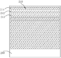
- FIG. 3 is a schematic view of a touch layer according to a first embodiment of the present invention.
- FIG. 4 is a schematic view of a capacitive touch screen according to a first embodiment of the present invention (the insulating layer is hidden);
- Figure 5 is a cross-sectional view showing a capacitive touch screen according to a first embodiment of the present invention
- FIG. 6 is a schematic diagram of the capacitive touch screen of the first embodiment of the present invention when it is not touched;
- FIG. 7 is a schematic diagram of a capacitive touch screen according to a first embodiment of the present invention.
- Figure 8 is a schematic view showing a conductive layer of a second embodiment of the present invention.
- FIG. 9 is a schematic view of a capacitive touch screen according to a second embodiment of the present invention (the insulating layer is hidden);
- the embodiment of the invention provides a capacitive touch screen.
- the capacitive touch screen includes a touch chip 230 , a conductive layer, an insulating layer 250 and a touch layer.
- the touch chip 230 can be used to emit a sensing signal for detecting a touch position, or can receive a signal of a charge change and process the signal, thereby obtaining a position where a charge change is generated, thereby obtaining a current position. Touch location.
- the touch chip 230 is located at the location The upper or lower side of the capacitive touch screen is located on the lower side of the capacitive touch screen in FIG.
- the conductive layer includes a conductive region 260 and a trace region 270, and the trace region 270 is located outside the conductive region 260, for example, at the left of the trace region 270.
- the conductive region 260 includes a plurality of separated conductive electrodes 240 that are parallel to each other and extend in the X-axis direction, that is, the conductive electrodes 240 extend from the left side to the left side.
- the conductive electrode 240 extends from the left end of the capacitive touch screen to a position at a distance from the right end, that is, a certain distance from the right end.
- the conductive electrode may also extend from the upper side to the lower side.
- the conductive electrodes 240 are elongated, and the lengths of the plurality of conductive electrodes 240 are different, and the left ends are on the same vertical line, but the right ends are on different vertical lines.
- the right ends of the plurality of conductive electrodes 240 from top to bottom are gradually inwardly retracted, that is, to the left, that is, sorted from top to bottom, at all the conductive electrodes 240.
- the right end of the first conductive electrode 241 is located at the rightmost side
- the right end of the second conductive electrode 242 is located on the right side
- the right end of the second conductive electrode 243 is located on the right side of the second
- the right end of the other conductive electrode 240 is located at the leftmost side.
- the present invention is not limited thereto.
- the lengths of the plurality of conductive electrodes are different, and the left and right ends of the plurality of conductive electrodes are gradually retracted from top to bottom, that is, gradually shrinking toward the middle. .
- the lengths of the plurality of conductive electrodes are different. Specifically, the right ends of the plurality of conductive electrodes are located on the same vertical line, and the left end thereof is gradually retracted from top to bottom.
- the trace area 270 is located at the right end of the conductive region 260 , specifically, the trace region 270 is the second conductive electrode 242 - the last conductive electrode 240 The area where the first conductive electrode 241 is vacated, so that the boundary line between the wiring area 270 and the conductive area 260 is stepped (see the broken line in FIG. 2).
- a plurality of separated transmission lines 220 are disposed in the routing area 270, the number of the transmission lines 220 is the same as the number of the conductive electrodes 240, and each of the conductive electrodes 240 is electrically connected to one of the above-mentioned conductive electrodes 240. Transmission line 220.
- the lower end of the right side of the conductive electrode 240 is electrically connected to the transmission line 220, where the transmission line 220 is perpendicular to the conductive electrode 240 electrically connected thereto, and thus the right end of the conductive electrode 240 is known.
- the transmission line 220 is perpendicular to the conductive electrode 240 electrically connected thereto, and thus the right end of the conductive electrode 240 is known.
- the transmission line 220 on the right side of the first conductive electrode 241 there is no transmission line 220 on the right side of the first conductive electrode 241 (the transmission line 220 electrically connected to the first conductive electrode 241 is on the lower side thereof), and a transmission line on the right side of the second conductive electrode 242
- the end of the transmission line 220 is electrically connected to the touch chip 230.
- the lower end of the transmission line 220 is electrically connected to the touch chip 230.
- the insulating layer 250 is located on the conductive layer, and the insulating layer 250 covers the conductive electrode 240 and the transmission line 220 .
- the material of the insulating layer 250 is SiO 2 , a silicon nitride compound, or the like.
- the touch layer is disposed on the insulating layer 250, the touch layer includes a plurality of separate touch electrodes 210, and the touch electrodes 210 and the The conductive electrodes 240 correspond to each other.
- the plurality of touch electrodes 210 are elongated, and the plurality of touch electrodes 210 are parallel to each other and extend along the X-axis direction, that is, the touch electrodes 210 extend from the left end of the capacitive touch screen.
- each touch electrode 210 is located above the corresponding one of the conductive electrodes 240 and parallel to the conductive electrodes 240. Additionally, in other embodiments of the invention, the conductive electrode may also extend from top to bottom. In this embodiment, the plurality of touch electrodes 210 have the same size, specifically the same length and width. In this embodiment, the area of the touch electrode 210 is greater than or equal to the area of any one of the conductive electrodes 240.
- the length dimension of the plurality of touch electrodes 210 is equal to the length dimension of the first conductive electrode 240, and the width of the plurality of touch electrodes 210 in the width direction is equal to the first conductive electrode 240.
- the width dimension, that is, the area of the first conductive electrode 241 is the same as the area of any one of the touch electrodes 210, and the area of the lower conductive electrode 240 is smaller than the area of any one of the touch electrodes 210.
- the touch electrode 210 of the touch layer is suspended from the conductive electrode 240. That is, the touch electrode 210 is not electrically connected to the conductive electrode 240 or the touch chip 230, but to the conductive electrode 240 and the touch chip 230. Maintain electrical insulation. Since the touch electrode 210 is not connected to the conductive electrode 240 and the touch chip 230 through the wire, the touch electrode 210 itself does not pass current, but generates an induced charge by inducing the charge of the conductive electrode 240. The induced charge of the touch electrode 210 is formed upward The electric field, and at the same time, forms a closed electric field with the charge of the conductive electrode 240. Therefore, the touch electrode 210 substantially forms a self-capacitance by the conductive electrode 240, and is not a mutual capacitance.
- the touch electrode 210 extends from above the conductive region 260 to above the trace region 270 .
- the first touch electrodes 211 cover the first conductive electrodes 241
- the second touch electrodes 212 cover the second conductive electrodes 242 and extend to the second conductive electrodes 242.
- the third touch electrode 213 covers the third conductive electrode 243 and extends to the two transmission lines 220 on the right side of the third conductive electrode 243
- the fourth touch electrode 210 covers the fourth.
- the conductive electrode 240 extends to the three transmission lines 220 on the right side of the fourth conductive electrode 240.
- the nth touch electrode 210 covers the nth conductive electrode 240 and extends to the right side of the nth conductive electrode 240. 1 transmission line 220, ....
- the touch electrode 210 and the corresponding conductive electrode 240 form a first capacitor C1
- the first capacitor C1 is a self-capacitance
- the touch electrode 210 forms a second capacitor C2 with the ground GND.
- Capacitor C1 and second capacitor C2 are connected in series (see Figure 6).
- the sensing signal is a voltage signal or a current signal
- the conductive electrode 240 is on the conductive electrode 240.
- a negative charge is accumulated.
- the corresponding touch electrode 210 is filled with a positive charge. Since the entire touch electrode 210 is an equipotential body, the corresponding touch electrode 210 on the transmission line 220 is also full. positive charge. Referring to FIG. 4 and FIG. 6 , when the touch chip 230 sends an inductive signal to the conductive electrode 240 , the sensing signal is a voltage signal or a current signal, and the conductive electrode 240 is on the conductive electrode 240. For example, a negative charge is accumulated. Due to the principle of capacitive coupling, the corresponding touch electrode 210 is filled with a positive charge. Since the entire touch electrode 210 is an equipotential body, the corresponding touch electrode 210 on the transmission line 220 is also full. positive charge. Referring to FIG.
- the touch chip 230 can detect the current through the transmission line 220. According to the current, the touch chip 230 can obtain which conductive electrode 240 or which conductive electrodes 240 change, when the conductive electrode is obtained. When there is a current on the transmission line 220 corresponding to 240, the current is a one-dimensional touch. When there is a current on the transmission line 220 corresponding to the plurality of conductive electrodes 240, the sliding control is performed at this time, and the user's finger is controlled by a touch electrode 210. The area slides to another area or touch areas.
- the touch electrode 210 extends to the routing area 270, so that when the user touches the capacitive touch screen area corresponding to the routing area 270, the user's finger and the corresponding touch electrode 210 appear.
- the three capacitors C3 cause the charge on the corresponding touch electrode 210 to change, thereby causing a change in the amount of charge on the corresponding conductive electrode 240, and the change is touched by current
- the control chip 230 detects that the touch chip 230 can obtain the touch position by calculation. Therefore, even if the user's finger touches the capacitive touch screen area corresponding to the routing area 270, the touch chip 230 can detect the touch position, thereby improving the problem of the touch dead zone in the background art, thereby improving the user experience.
- the capacitive touch screen of the embodiment of the invention has a simple structure and a low cost.
- the sensing signal sent by the touch chip 230 to the conductive electrode 240 through the transmission line 220 is an alternating current signal, so that the polarity of the charge on the conductive electrode 240 changes periodically, for example, at a certain time period.
- the conductive electrode 240 has a negative charge, and the conductive electrode 240 has a positive charge for the next period of time, and the polarity of the charge on the touch electrode 210 changes periodically.
- the insulating layer 250 between the conductive electrode 240 and the touch electrode 210 may not be too thick; and, in order to prevent the first capacitor from being easily broken down, The insulating layer 250 should also not be too thin.
- the thickness of the insulating layer 250 ranges from 0.01 mm to 1.0 mm, for example, 0.01 mm, 0.05 mm, 0.1 mm, 0.2 mm, 0.3 mm, 0.4 mm, 0.5 mm, 0.6 mm, 0.7 mm, 0.8mm, 0.9mm, 1.0mm, etc.
- the capacitive touch screen further includes a protective layer 280 and a base substrate 290.
- the protective layer 280 is located on the touch electrode 210, and the base substrate 290 is located below the conductive layer. .
- the touch electrode 210 is located on the protection layer 280
- the insulating layer 250 is located on the touch electrode 210
- the conductive layer is located on the insulating layer 250
- the base substrate 290 is located on the conductive layer.
- the touch chip 230 is actually located on the base substrate 290.
- the capacitive touch screen further includes a flexible circuit board, the flexible circuit board is bonded on the base substrate, and the touch chip is located The flexible circuit board.
- FIG. 9 is a schematic diagram of a capacitive touch screen according to a second embodiment of the present invention.
- the schematic diagram of FIG. 9 is similar to the schematic diagram of FIG. 4, and thus the same component symbols represent the same components.
- the main difference between this embodiment and the second embodiment is the connection of the transmission line and the conductive electrode.
- the conductive layer includes a conductive region 360 and a trace region 370 , and the trace regions 370 are located on opposite sides of the conductive region 360 .
- the conductive region 360 is provided with a plurality of separated conductive electrodes 340, and the conductive electrodes 340 are elongated and extend from the left side to the right side.
- the plurality of conductive electrodes 340 have the same area, that is, their lengths and widths are the same.
- the routing area 370 is located on the left and right sides of the conductive area 260, that is, has two routing areas 370, wherein a plurality of transmission lines are disposed in the left side routing area 370.
- the number of the transmission lines 320 in the routing area 370 on the left side is equal to the number of the conductive electrodes 340. One end of each transmission line 320 is electrically connected to the corresponding conductive electrode 340, and the other end is electrically connected to the touch chip 230. Similarly, the same number of transmission lines 320 are provided in the routing area 370 on the right side, and the corresponding one of the transmission lines 370 in the right side line area 370 is electrically connected to the corresponding conductive electrode 340. One end is electrically connected to the touch chip 230. That is, the left and right ends of the same conductive electrode 340 are electrically connected to the touch chip 230 through a transmission line 320, respectively. Therefore, the touch chip 230 is more sensitive to receive the current signal and transmit the sensing signal.
- the touch layer includes a plurality of separate touch electrodes 310, the touch electrodes 310 extend from the left side to the right side, and the number of the touch electrodes 310 and the conductive electrodes 340
- the number of touch electrodes 310 is the same as that of one conductive electrode 340.
- the plurality of touch electrodes 310 have the same area, that is, the plurality of touch electrodes 310 have the same length and width.
- the area of any one of the touch electrodes 310 is larger than the area of any one of the conductive electrodes 340.
- any one of the touch electrodes 310 is greater than or equal to the width of any one of the conductive electrodes 340, and any one of the touch electrodes 310 The length is greater than the length of any one of the conductive electrodes 340.
- any one of the touch electrodes 310 covers the corresponding conductive electrode 340 and covers the transmission line 320 connected to the corresponding one of the conductive electrodes 340.
- the touch electrode 310 extends to the left to the left trace area 370.
- a transmission line 320 on the left side connected to the corresponding conductive electrode 340 is covered, extending rightward to the right of the right wiring area 370, covering the transmission line 320 on the right side connected to the corresponding conductive electrode 340.
- the transmission line 320 includes a first segment adjacent to the conductive electrode 340 electrically connected thereto and a second segment electrically connected to the conductive electrode 340 away therefrom, and the conductive electrode
- the corresponding touch electrode 310 of the 340 covers the first electrode of the conductive electrode 340 and the transmission line 320 electrically connected to the conductive electrode 340.
- the first segment is a horizontal setting
- the second segment is longitudinally disposed, and the second segment of the transmission line 320 is covered by the touch electrode 310 corresponding to the lower conductive electrode 340.
- the transmission line 320 also includes a first segment adjacent to the conductive electrode 340 electrically connected thereto and a second segment remote from the conductive electrode 340 electrically connected thereto, corresponding to the conductive electrode 340
- the touch electrode 310 covers the conductive electrode 340 and a first segment of the transmission line 320 electrically connected to the conductive electrode 340.
- the second segment of the transmission line 320 is covered by the touch electrode 310 corresponding to the lower conductive electrode 340.
Landscapes
- Engineering & Computer Science (AREA)
- General Engineering & Computer Science (AREA)
- Theoretical Computer Science (AREA)
- Human Computer Interaction (AREA)
- Physics & Mathematics (AREA)
- General Physics & Mathematics (AREA)
- Position Input By Displaying (AREA)
Abstract
本发明实施例公开了一种电容触摸屏,包括:触控芯片;导电层,其包括导电区和走线区,所述导电区内设有多条分离的导电电极,所述走线区设有多条分离的传输线,每条导电电极通过所述传输线与所述触控芯片电连接;绝缘层,其位于所述导电层上;触控层,其位于绝缘层的上方,所述触控层包括多条分离的触控电极,所述触控电极与所述导电电极相对应,且至少部分所述触控电极延伸到所述走线区的上方;其中,当触摸所述电容触摸屏时,所述触控电极上的电荷变化引起对应导电电极上的电荷变化,所述触控芯片通过传输线获知导电电极上的电荷变化以用于判断触摸位置。采用本发明,具有改善用户的触摸体验的优点。
Description
本发明涉及一种触摸领域,特别涉及一种电容触摸屏。
现有的电容触摸屏,请参见图1,包括触控芯片130、多条长条形的触控电极110、多条传输线120,其中,所述触控芯片130位于所述电容触摸屏的下端,多条所述触控电极110位于所述触控芯片130的上侧,多条所述触控电极110彼此互相平行,并沿X轴方向延伸,每个所述触控电极110的左右两侧分别通过传输线120电连接到所述触控芯片130。从而,触控芯片130通过传输线120发送感应信号给多条所述触控电极110,所述触控电极110与地形成第一电容。此种电容式触摸屏可以侦测滑控和一维位置。当用户的手指触摸所述触控电极110时,用户手指会与触控电极110形成第二电容,从而造成触控电极110上电荷发生变化,所述触控芯片130侦测到该变化,进而获得用户的手指的位置或动作。
在使用上述的电容触摸屏时,由于电容触摸屏的左右两侧边缘需要留下空间供传输线120走线,而当用户触摸到传输线120所处的位置时,此时触控电极110不能识别,也即传输线120所处的区域为触控盲区,从而造成用户的体验较差。
发明内容
本发明实施例所要解决的技术问题在于,提供一种电容触摸屏。改善了用户的触摸体验,减少了触控盲区。
为了解决上述技术问题,本发明实施例提供了一种检电容触摸屏,包括:
触控芯片;
导电层,其包括导电区和走线区,所述导电区内设有多条分离的导电电极,所述走线区设有多条分离的传输线,每条导电电极通过所述传输线与所述触控
芯片电连接;
绝缘层,其位于所述导电层上;
触控层,其位于绝缘层的上方,所述触控层包括多条分离的触控电极,所述触控电极与所述导电电极相对应,且至少部分所述触控电极延伸到所述走线区的上方;其中,
当触摸所述电容触摸屏时,所述触控电极上的电荷变化引起对应导电电极上的电荷变化,所述触控芯片通过传输线获知导电电极上的电荷变化以用于判断触摸位置。
实施本发明实施例,具有如下有益效果:
由于所述触控电极延伸到走线区,从而当用户手指触摸到走线区对应的电容触摸屏区域时,用户手指与对应的触控电极出现第三电容,从而导致对应的触控电极上感应的电荷量发生变化,进而导致对应的导电电极上的电荷量发生变化,该变化被触控芯片侦测到,从而触控芯片可以通过计算获得触控位置。从而,即使用户的手指触摸到走线区对应的电容触摸屏区域,触控芯片也能侦测得到触控位置,从而改善了背景技术中触控盲区的问题,从而改善了用户的体验。而且本发明实施例的电容触摸屏结构简单、成本较低。
为了更清楚地说明本发明实施例或现有技术中的技术方案,下面将对实施例或现有技术描述中所需要使用的附图作简单地介绍,显而易见地,下面描述中的附图仅仅是本发明的一些实施例,对于本领域普通技术人员来讲,在不付出创造性劳动的前提下,还可以根据这些附图获得其他的附图。
图1是现有技术一种电容触摸屏的示意图;
图2是本发明第一实施例导电层的示意图;
图3是本发明第一实施例触控层的示意图;
图4是本发明第一实施例电容触摸屏的示意图(隐藏了绝缘层);
图5是本发明第一实施例电容触摸屏的剖视图;
图6是本发明第一实施例电容触摸屏未触摸时的示意图;
图7是本发明第一实施例电容触摸屏被触摸时的示意图;
图8是本发明第二实施例导电层的示意图;
图9是本发明第二实施例电容触摸屏的示意图(隐藏了绝缘层);
图示标号:
110、210、310-触控电极;211-第一条触控电极;212-第二条触控电极;213-第三条触控电极;120、220、320-传输线;130、230-触控芯片;240、340-导电电极;241-第一条导电电极;242-第二条导电电极;243-第三条导电电极;250-绝缘层;260、360-导电层;270、370-走线区;280-保护层;290-衬底基板。
下面将结合本发明实施例中的附图,对本发明实施例中的技术方案进行清楚、完整地描述,显然,所描述的实施例仅仅是本发明一部分实施例,而不是全部的实施例。基于本发明中的实施例,本领域普通技术人员在没有作出创造性劳动前提下所获得的所有其他实施例,都属于本发明保护的范围。
本申请说明书、权利要求书和附图中出现的术语“包括”和“具有”以及它们任何变形,意图在于覆盖不排他的包含。例如包含了一系列步骤或单元的过程、方法、系统、产品或设备没有限定于已列出的步骤或单元,而是可选地还包括没有列出的步骤或单元,或可选地还包括对于这些过程、方法、产品或设备固有的其它步骤或单元。此外,术语“第一”、“第二”和“第三”等是用于区别不同的对象,而并非用于描述特定的顺序。
第一实施例
本发明实施例提供一种电容触摸屏,请参见图2-图7,所述电容触摸屏包括触控芯片230、导电层、绝缘层250和触控层。
在本实施例中,所述触控芯片230可以用于发出感应信号以用于侦测触摸位置,也可以接收电荷变化的信号并对信号进行处理,从而获得产生电荷变化的位置,进而获得当前的触控位置。在本实施例中,所述触控芯片230位于所
述电容触摸屏的上侧或者下侧,在图2中为位于电容触摸屏的下侧。
在本实施例中,请参见图2,所述导电层包括导电区260和走线区270,所述走线区270位于所述导电区260的外侧,例如位于所述走线区270的左侧、右侧、上侧(此时触控芯片230位于左侧或右侧)、下侧(此时触控芯片230位于左侧或右侧)等,在本实施例中所述走线区270位于所述导电区260的右侧。在本实施例中,所述导电区260包括多条分离的导电电极240,所述多条分离的导电电极240彼此互相平行且沿X轴方向延伸,也即导电电极240均从左侧延伸到右侧,在本实施例中,所述导电电极240从电容触摸屏的左端延伸到距离右端有一定距离的位置,也即距离右端具有一定间隔。当然,在本发明的其他实施例中,所述导电电极还可以从上侧延伸到下侧。在本实施例中,所述导电电极240呈长条形,多条所述导电电极240的长度不相同,其左端位于同一条竖直线上,但右端在不同的竖直线上。具体说来,在本实施例中,从上到下多条所述导电电极240的右端依序逐步向内缩,也即向左缩,也即:从上到下排序,在所有导电电极240中第一条导电电极241的右端位于最右侧,第二条导电电极242的右端位于次右侧,第二条导电电极243的右端位于次次右侧,…,最后一条导电电极240的右端相对其他导电电极240的右端位于最左侧。但本发明不限于此,在发明的实施例中,多条所述导电电极的长度不相同,从上到下多条所述导电电极的左右两端均逐步内缩,也即逐步向中间收缩。在本发明的其他实施例中,多条所述导电电极的长度不相同,具体为多条所述导电电极的右端位于同一竖直线上,其左端从上到下逐步内缩。
在本实施例中,请继续参见图2,所述走线区270位于所述导电区260的右端,具体说来,所述走线区270为第二条导电电极242-最后一条导电电极240相对第一条导电电极241空出的区域,从而,所述走线区270与所述导电区260之间的分界线呈阶梯型(请参见图2中的虚线)。在本实施例中,所述走线区270内设有多条分离的传输线220,所述传输线220的数量与所述导电电极240的数量相同,每条所述导电电极240电连接一条所述传输线220。具体说来,所述导电电极240的右侧下端电连接所述传输线220,在此处所述传输线220垂直于与其电连接的导电电极240,由此可知,所述导电电极240的右端之所以要向内缩,是为了空出右侧区域用于传输线220的走线,避免传输
线220与导电电极240互相干涉。在本实施例中,第一条导电电极241的右侧没有传输线220存在(与第一条导电电极241电连接的传输线220在其下侧),第二条导电电极242的右侧有一条传输线220存在,第三条导电电极243的右侧有两条传输线220存在,…,第n条导电电极240的右侧有n-1条传输线220存在(n为大于或等于2的整数),…。在本实施例中,所述传输线220远离导电电极240的一端电连接所述触控芯片230,在本实施例中,所述传输线220的下端电连接所述触控芯片230。
在本实施例中,请参见图5,所述绝缘层250位于所述导电层上,所述绝缘层250覆盖所述导电电极240、传输线220。在本实施例中,所述绝缘层250的材料为SiO2、氮硅化合物等。
在本实施例中,请参见图2-图4,所述触控层位于所述绝缘层250上,所述触控层包括多条分离的触控电极210,所述触控电极210与所述导电电极240相对应。在本实施例中,多条所述触控电极210呈长条形,多条所述触控电极210彼此互相平行且沿X轴方向延伸,也即触控电极210均从电容触摸屏的左端延伸到相对的另一端,也即右端,且触控电极210的数目与所述导电电极240的数目相同,每条触控电极210位于对应一条导电电极240的上方,且与导电电极240平行。另外,在本发明的其他实施例中,所述导电电极还可以从上向下延伸。在本实施例中,多条所述触控电极210的尺寸相同,具体为长度尺寸、宽度尺寸相同。在本实施例中,所述触控电极210的面积大于或等于任意一个导电电极240的面积。具体说来,多条所述触控电极210的长度尺寸等于第一条所述导电电极240的长度尺寸,多条所述触控电极210宽度方向的尺寸等于第一条所述导电电极240的宽度尺寸,也即第一条导电电极241的面积与任意一个触控电极210的面积相同,下面的导电电极240的面积小于任意一个触控电极210的面积。
触控层的触控电极210相对于导电电极240为悬浮设置,也就是说,触控电极210未与导电电极240或是触控芯片230电连接,而是与导电电极240及触控芯片230保持电绝缘的状态。由于触控电极210并未通过导线与导电电极240和触控芯片230连接,因此触控电极210本身无电流通过,而是通过感应导电电极240的电荷产生感应电荷。触控电极210的感应电荷向上形成开放
电场,并同时向下与导电电极240的电荷形成封闭电场。因此,触控电极210借助导电电极240实质上形成了自电容,而并非互电容。
在本实施例中,请参见图4,至少部分所述触控电极210从导电区260的上方延伸到走线区270的上方。具体说来,从上往下排序,第一条触控电极211覆盖所述第一条导电电极241,第二条触控电极212覆盖第二条导电电极242并延伸到第二条导电电极242右侧的一条传输线220上,第三条触控电极213覆盖第三条导电电极243并延伸到第三条导电电极243右侧的两条传输线220上,第四条触控电极210覆盖第四条导电电极240并延伸到第四条导电电极240右侧三条传输线220上,…,第n条触控电极210覆盖第n条导电电极240并延伸到第n条导电电极240右侧的n-1条传输线220上,…。在本实施例中,所述触控电极210与对应的导电电极240形成第一电容C1,该第一电容C1为自电容,所述触控电极210与地GND形成第二电容C2,第一电容C1和第二电容C2串联(请参见图6)。
在本实施例中,请参见图4和图6,当所述触控芯片230发送感应信号给所述导电电极240时,该感应信号为电压信号或电流信号,此时所述导电电极240上积满例如负电荷,由于电容耦合原理,对应的触控电极210上积满正电荷,由于整条触控电极210为一个等势体,从而传输线220上对应的触控电极210部分也积满正电荷。请参见图7,当用户手指触摸电容触摸屏时,此时用户手指与触控电极210形成第三电容C3,从而使触控电极210上的正电荷的电荷量发生变化,进而导致对应导电电极240上电荷量发生变化,此时触控芯片230通过传输线220可以侦测到电流,触控芯片230根据该电流可以获得是哪条导电电极240或者哪些导电电极240发生变化,当获得是一条导电电极240对应的传输线220上存在电流时,此时为一维触控,当获得是多条导电电极240对应的传输线220上存在电流时,此时为滑控,用户手指由一条触控电极210的区域滑到另外一条或者多条触控的区域。
从而,在本实施例中,由于所述触控电极210延伸到走线区270,从而当用户手指触摸到走线区270对应的电容触摸屏区域时,用户手指与对应的触控电极210出现第三电容C3,从而导致对应的触控电极210上的电荷发生变化,进而导致对应的导电电极240上的电荷量发生变化,该变化以电流的方式被触
控芯片230侦测到,从而触控芯片230可以通过计算获得触控位置。从而,即使用户的手指触摸到走线区270对应的电容触摸屏区域,触控芯片230也能侦测得到触控位置,从而改善了背景技术中触控盲区的问题,从而改善了用户的体验。而且本发明实施例的电容触摸屏结构简单、成本较低。
在本实施例中,所述触控芯片230通过传输线220发送给导电电极240的感应信号为交流信号,从而所述导电电极240上的电荷的极性呈周期性变化,例如在某个时间段导电电极240上为负电荷,在接下来的时间段导电电极240上为正电荷,所述触控电极210上电荷的极性对应呈周期性变化。
在本实施例中,为了使第一电容比较灵敏,所述导电电极240与所述触控电极210之间的绝缘层250不能太厚;而且,为了防止第一电容被轻易击穿,所述绝缘层250也不能太薄。在本实施例中,所述绝缘层250的厚度范围为0.01mm-1.0mm,例如为0.01mm、0.05mm、0.1mm、0.2mm、0.3mm、0.4mm、0.5mm、0.6mm、0.7mm、0.8mm、0.9mm、1.0mm等。
另外,在本实施例中,所述电容触摸屏还包括保护层280和衬底基板290,所述保护层280位于所述触控电极210上,所述衬底基板290位于所述导电层的下方。实际如果从上往下看,请参见图5,也可以看做所述触控电极210位于所述保护层280上,所述绝缘层250位于所述触控电极210上,所述导电层位于所述绝缘层250上,所述衬底基板290位于所述导电层上。从而,用户触摸电容触摸屏时,用户实际是触摸到该保护层280。
另外,在本实施例中,所述触控芯片230实际位于所述衬底基板290上。但本发明不限于此,在本发明的其他实施例中,所述电容触摸屏还包括柔性电路板,所述柔性电路板绑定(bonding)在所述衬底基板上,所述触控芯片位于所述柔性电路板上。
第二实施例
图9是本发明第二实施例的电容触摸屏的示意图,图9的示意图与图4的示意图相似,因此相同的元件符号代表相同的元器件。本实施例与第二实施例的主要不同点为传输线与导电电极的连接。
请参见图8、图9,在本实施例中,所述导电层包括导电区360和走线区370,所述走线区370位于所述导电区360的相对两侧。具体说来,所述导电区360内设有多条分离的导电电极340,所述导电电极340呈长条形,且由左侧延伸到右侧。在本实施例中,多条所述导电电极340的面积相等,也即它们的长度和宽度相同。在本实施例中,所述走线区370位于所述导电区260的左侧和右侧,也即具有两个走线区370,其中,左侧的走线区370内设有多条传输线320,左侧的走线区370内设有的传输线320的数目等于所述导电电极340的数目,每条传输线320的其中一端电连接对应的导电电极340,另一端电连接到触控芯片230;同样,右侧的走线区370内设有与左侧的走线区370内相同数目的传输线320,右侧走线区370内每条传输的其中一端电连接对应的导电电极340,另一端电连接到触控芯片230。也即,同一条导电电极340的左右两端分别通过一条传输线320电连接到触控芯片230。从而,触控芯片230接收电流信号和传输感应信号都比较灵敏。
在本实施例中,所述触控层包括多条分离的触控电极310,所述触控电极310从左侧延伸到右侧,所述触控电极310的数目与所述导电电极340的数目相同,一条触控电极310对应一条导电电极340设置。在本实施例中,多条所述触控电极310的面积相同,也即多条所述触控电极310的长度和宽度相同。在本实施例中,任意一条触控电极310的面积大于任意一条导电电极340的面积,具体为任意一条触控电极310的宽度大于或等于任意一条导电电极340的宽度,任意一条触控电极310的长度大于任意一条导电电极340的长度。具体说来,任意一条触控电极310覆盖相应的导电电极340,并覆盖与该相应的一导电电极340连接的传输线320,具体为所述触控电极310向左延伸到左侧走线区370的上方,覆盖了与相应的导电电极340连接的左侧的传输线320,向右延伸到右侧走线区370的上方,覆盖了与相应的导电电极340连接的右侧的传输线320。
在本实施例中,请参见左侧的走线区370,所述传输线320包括靠近与其电连接的导电电极340的第一段和远离与其电连接导电电极340的第二段,与该导电电极340相对应的触控电极310覆盖该导电电极340及与该导电电极340电连接的传输线320的第一段。在本实施例中,所述第一段为横向设置,
所述第二段为纵向设置,所述传输线320的第二段被下面的导电电极340对应的触控电极310所覆盖。同样,在右侧的走线区370,所述传输线320也包括靠近与其电连接的导电电极340的第一段和远离与其电连接导电电极340的第二段,与该导电电极340相对应的触控电极310覆盖该导电电极340及与该导电电极340电连接的传输线320的第一段,该传输线320的第二段被下面的导电电极340对应的触控电极310所覆盖。
需要说明的是,本说明书中的各个实施例均采用递进的方式描述,每个实施例重点说明的都是与其它实施例的不同之处,各个实施例之间相同相似的部分互相参见即可。对于装置实施例而言,由于其与方法实施例基本相似,所以描述的比较简单,相关之处参见方法实施例的部分说明即可。
以上所揭露的仅为本发明较佳实施例而已,当然不能以此来限定本发明之权利范围,因此依本发明权利要求所作的等同变化,仍属本发明所涵盖的范围。
Claims (18)
- 一种电容触摸屏,其特征在于,包括:触控芯片;导电层,其包括导电区和走线区,所述导电区内设有多条分离的导电电极,所述走线区设有多条分离的传输线,每条导电电极通过所述传输线与所述触控芯片电连接;绝缘层,其位于所述导电层上;触控层,其位于绝缘层的上方,所述触控层包括多条分离的触控电极,所述触控电极与所述导电电极相对应,且至少部分所述触控电极延伸到所述走线区的上方;其中,当触摸所述电容触摸屏时,所述触控电极上的电荷变化引起对应导电电极上的电荷变化,所述触控芯片通过传输线获知导电电极上的电荷变化以用于判断触摸位置。
- 如权利要求1所述的电容触摸屏,其特征在于,触控电极向上形成开放电场,触控电极向下与导电电极形成封闭电场。
- 如权利要求1所述的电容触摸屏,其特征在于,触控电极未电连接导电电极及触控芯片。
- 如权利要求1所述的电容触摸屏,其特征在于,触控电极上的电荷为感应导电电极的电荷所产生的感应电荷。
- 如权利要求1所述的电容触摸屏,其特征在于,多条所述导电电极的第一端向内依序逐渐收缩,所述走线区位于所述导电电极收缩的位置处。
- 如权利要求5所述的电容触摸屏,其特征在于,所述走线区邻近导电区的边缘线为阶梯型。
- 如权利要求1所述的电容触摸屏,其特征在于,所述绝缘层的厚度范围为0.01mm-1.0mm。
- 如权利要求1所述的电容触摸屏,其特征在于,所述传输线的一端与所述导电电极靠近触控芯片一侧电连接。
- 如权利要求1所述的电容触摸屏,其特征在于,所述触控电极覆盖相应的一导电电极及与该相应的一导电电极连接的传输线。
- 如权利要求9所述的电容触摸屏,其特征在于,该相应的一导电电极连接的传输线垂直于该相应的一导电电极。
- 如权利要求9所述的电容触摸屏,其特征在于,该相应的一导电电极连接的传输线包括靠近该相应的一导电电极的第一段及远离该相应的一导电电极的第二段,每一触控电极覆盖该相应的一导电电极及与该相应的一导电电极连接的传输线的第一段。
- 如权利要求11所述的电容触摸屏,其特征在于,与该相应的一导电电极连接的传输线的第二段被另一触控电极所覆盖。
- 如权利要求1所述的电容触摸屏,其特征在于,触控电极与地之间形成第二电容,触控电极与导电电极之间形成第一电容,第一电容与第二电容串联。
- 如权利要求1所述的电容触摸屏,其特征在于,所述走线区位于所述导电区的相对两侧,每条导电电极的两端分别与传输线电连接,两条该传输线电连接到触控芯片。
- 如权利要求1所述的电容触摸屏,其特征在于,任意一个所述导电电极的面积小于或等于任意一个触控电极的面积。
- 如权利要求1所述的电容触摸屏,其特征在于,所述导电电极上电荷的极性呈周期性变化。
- 如权利要求4所述的电容触摸屏,其特征在于,当触碰触控电极时,触碰引起触控电极上原有的感应电荷量发生变化,触控电极的感应电荷量变化导致导电电极上的电荷变化,进而判断出被触碰的触控电极的位置。
- 如权利要求1所述的电容触摸屏,其特征在于,触控电极从电容触摸屏的一端延伸至相对另一端,导电电极从电容触摸屏的一端延伸至与相对另一端间隔的位置。
Priority Applications (2)
| Application Number | Priority Date | Filing Date | Title |
|---|---|---|---|
| CN201780096910.6A CN111356973A (zh) | 2017-11-28 | 2017-11-28 | 电容触摸屏 |
| PCT/CN2017/113271 WO2019104458A1 (zh) | 2017-11-28 | 2017-11-28 | 电容触摸屏 |
Applications Claiming Priority (1)
| Application Number | Priority Date | Filing Date | Title |
|---|---|---|---|
| PCT/CN2017/113271 WO2019104458A1 (zh) | 2017-11-28 | 2017-11-28 | 电容触摸屏 |
Publications (1)
| Publication Number | Publication Date |
|---|---|
| WO2019104458A1 true WO2019104458A1 (zh) | 2019-06-06 |
Family
ID=66663711
Family Applications (1)
| Application Number | Title | Priority Date | Filing Date |
|---|---|---|---|
| PCT/CN2017/113271 Ceased WO2019104458A1 (zh) | 2017-11-28 | 2017-11-28 | 电容触摸屏 |
Country Status (2)
| Country | Link |
|---|---|
| CN (1) | CN111356973A (zh) |
| WO (1) | WO2019104458A1 (zh) |
Citations (4)
| Publication number | Priority date | Publication date | Assignee | Title |
|---|---|---|---|---|
| US5432671A (en) * | 1990-02-19 | 1995-07-11 | Mors Composants | Device forming tactile screen of the capacitive type |
| CN101566900A (zh) * | 2008-04-15 | 2009-10-28 | 株式会社日立显示器 | 显示装置 |
| CN104111749A (zh) * | 2013-04-19 | 2014-10-22 | 三星显示有限公司 | 显示装置 |
| CN106325622A (zh) * | 2015-06-26 | 2017-01-11 | 小米科技有限责任公司 | 自电容式压力触摸装置及终端设备 |
Family Cites Families (1)
| Publication number | Priority date | Publication date | Assignee | Title |
|---|---|---|---|---|
| CN105117081B (zh) * | 2015-08-14 | 2019-02-19 | 京东方科技集团股份有限公司 | 触控基板及其制造方法、触摸显示装置 |
-
2017
- 2017-11-28 WO PCT/CN2017/113271 patent/WO2019104458A1/zh not_active Ceased
- 2017-11-28 CN CN201780096910.6A patent/CN111356973A/zh active Pending
Patent Citations (4)
| Publication number | Priority date | Publication date | Assignee | Title |
|---|---|---|---|---|
| US5432671A (en) * | 1990-02-19 | 1995-07-11 | Mors Composants | Device forming tactile screen of the capacitive type |
| CN101566900A (zh) * | 2008-04-15 | 2009-10-28 | 株式会社日立显示器 | 显示装置 |
| CN104111749A (zh) * | 2013-04-19 | 2014-10-22 | 三星显示有限公司 | 显示装置 |
| CN106325622A (zh) * | 2015-06-26 | 2017-01-11 | 小米科技有限责任公司 | 自电容式压力触摸装置及终端设备 |
Also Published As
| Publication number | Publication date |
|---|---|
| CN111356973A (zh) | 2020-06-30 |
Similar Documents
| Publication | Publication Date | Title |
|---|---|---|
| US8970523B2 (en) | Two-dimensional capacitive touch panel with single sensor layer | |
| US10067615B2 (en) | Electrostatic capacitive touch-sensitive panel improving touch accuracy of edge regions | |
| CN104182081B (zh) | 触控感测电极结构及触控装置 | |
| US8988383B2 (en) | Electrostatic capacitive type touch screen panel | |
| US10394404B2 (en) | Touch display panel | |
| US10248265B2 (en) | Touch detecting panel | |
| TWI543053B (zh) | 觸控感應裝置 | |
| KR102247135B1 (ko) | 정전용량식 터치 감지 패널 | |
| US20140110236A1 (en) | Touch screen panel | |
| KR20160021379A (ko) | 터치 스크린 패널 | |
| US20170350771A1 (en) | Force sensor with noise shielding layer | |
| KR20150077133A (ko) | 터치 패널 및 이를 포함하는 표시 장치 | |
| CN103309494A (zh) | 位于触控感测元件上的电极单元 | |
| CN106406644A (zh) | 触摸屏面板 | |
| KR101956139B1 (ko) | 터치 패널 | |
| WO2019104458A1 (zh) | 电容触摸屏 | |
| WO2015043047A1 (zh) | 一种互电容式的触摸屏 | |
| TW201241708A (en) | Capacitance sensor structure | |
| TWM486811U (zh) | 感應層電路結構 | |
| TWI567623B (zh) | 觸控面板以及在觸控表面有改良電阻特徵之均勻敏感度的觸控輸入裝置 | |
| CN103336643A (zh) | 触控面板 | |
| CN109308145A (zh) | 一种等电阻驱动线布线结构及制备方法 | |
| CN109766033B (zh) | 触控显示面板 | |
| KR102095241B1 (ko) | 터치 스크린 패널 | |
| KR102325082B1 (ko) | 터치 스크린 패널 |
Legal Events
| Date | Code | Title | Description |
|---|---|---|---|
| 121 | Ep: the epo has been informed by wipo that ep was designated in this application |
Ref document number: 17933834 Country of ref document: EP Kind code of ref document: A1 |
|
| NENP | Non-entry into the national phase |
Ref country code: DE |
|
| 122 | Ep: pct application non-entry in european phase |
Ref document number: 17933834 Country of ref document: EP Kind code of ref document: A1 |