WO2019065003A1 - レーザ照射装置、レーザ照射方法及び投影マスク - Google Patents
レーザ照射装置、レーザ照射方法及び投影マスク Download PDFInfo
- Publication number
- WO2019065003A1 WO2019065003A1 PCT/JP2018/030866 JP2018030866W WO2019065003A1 WO 2019065003 A1 WO2019065003 A1 WO 2019065003A1 JP 2018030866 W JP2018030866 W JP 2018030866W WO 2019065003 A1 WO2019065003 A1 WO 2019065003A1
- Authority
- WO
- WIPO (PCT)
- Prior art keywords
- projection
- microlenses
- transmittance
- thin film
- openings
- Prior art date
- Legal status (The legal status is an assumption and is not a legal conclusion. Google has not performed a legal analysis and makes no representation as to the accuracy of the status listed.)
- Ceased
Links
Images






Classifications
-
- H—ELECTRICITY
- H10—SEMICONDUCTOR DEVICES; ELECTRIC SOLID-STATE DEVICES NOT OTHERWISE PROVIDED FOR
- H10P—GENERIC PROCESSES OR APPARATUS FOR THE MANUFACTURE OR TREATMENT OF DEVICES COVERED BY CLASS H10
- H10P14/00—Formation of materials, e.g. in the shape of layers or pillars
- H10P14/20—Formation of materials, e.g. in the shape of layers or pillars of semiconductor materials
- H10P14/38—Formation of materials, e.g. in the shape of layers or pillars of semiconductor materials characterised by treatments done after the formation of the materials
- H10P14/3802—Crystallisation or recrystallisation of non-monocrystalline semiconductor materials, e.g. regrowth
- H10P14/3808—Crystallisation or recrystallisation of non-monocrystalline semiconductor materials, e.g. regrowth using laser beams
- H10P14/381—Beam shaping, e.g. using a mask
-
- B—PERFORMING OPERATIONS; TRANSPORTING
- B23—MACHINE TOOLS; METAL-WORKING NOT OTHERWISE PROVIDED FOR
- B23K—SOLDERING OR UNSOLDERING; WELDING; CLADDING OR PLATING BY SOLDERING OR WELDING; CUTTING BY APPLYING HEAT LOCALLY, e.g. FLAME CUTTING; WORKING BY LASER BEAM
- B23K26/00—Working by laser beam, e.g. welding, cutting or boring
- B23K26/02—Positioning or observing the workpiece, e.g. with respect to the point of impact; Aligning, aiming or focusing the laser beam
- B23K26/06—Shaping the laser beam, e.g. by masks or multi-focusing
- B23K26/064—Shaping the laser beam, e.g. by masks or multi-focusing by means of optical elements, e.g. lenses, mirrors or prisms
- B23K26/066—Shaping the laser beam, e.g. by masks or multi-focusing by means of optical elements, e.g. lenses, mirrors or prisms by using masks
-
- B—PERFORMING OPERATIONS; TRANSPORTING
- B23—MACHINE TOOLS; METAL-WORKING NOT OTHERWISE PROVIDED FOR
- B23K—SOLDERING OR UNSOLDERING; WELDING; CLADDING OR PLATING BY SOLDERING OR WELDING; CUTTING BY APPLYING HEAT LOCALLY, e.g. FLAME CUTTING; WORKING BY LASER BEAM
- B23K26/00—Working by laser beam, e.g. welding, cutting or boring
- B23K26/50—Working by transmitting the laser beam through or within the workpiece
- B23K26/53—Working by transmitting the laser beam through or within the workpiece for modifying or reforming the material inside the workpiece, e.g. for producing break initiation cracks
-
- G—PHYSICS
- G02—OPTICS
- G02B—OPTICAL ELEMENTS, SYSTEMS OR APPARATUS
- G02B3/00—Simple or compound lenses
- G02B3/0006—Arrays
- G02B3/0037—Arrays characterized by the distribution or form of lenses
-
- G—PHYSICS
- G02—OPTICS
- G02B—OPTICAL ELEMENTS, SYSTEMS OR APPARATUS
- G02B3/00—Simple or compound lenses
- G02B3/0006—Arrays
- G02B3/0037—Arrays characterized by the distribution or form of lenses
- G02B3/0056—Arrays characterized by the distribution or form of lenses arranged along two different directions in a plane, e.g. honeycomb arrangement of lenses
-
- G—PHYSICS
- G02—OPTICS
- G02B—OPTICAL ELEMENTS, SYSTEMS OR APPARATUS
- G02B3/00—Simple or compound lenses
- G02B3/0006—Arrays
- G02B3/0037—Arrays characterized by the distribution or form of lenses
- G02B3/0062—Stacked lens arrays, i.e. refractive surfaces arranged in at least two planes, without structurally separate optical elements in-between
- G02B3/0068—Stacked lens arrays, i.e. refractive surfaces arranged in at least two planes, without structurally separate optical elements in-between arranged in a single integral body or plate, e.g. laminates or hybrid structures with other optical elements
-
- G—PHYSICS
- G02—OPTICS
- G02B—OPTICAL ELEMENTS, SYSTEMS OR APPARATUS
- G02B5/00—Optical elements other than lenses
- G02B5/003—Light absorbing elements
-
- H—ELECTRICITY
- H10—SEMICONDUCTOR DEVICES; ELECTRIC SOLID-STATE DEVICES NOT OTHERWISE PROVIDED FOR
- H10D—INORGANIC ELECTRIC SEMICONDUCTOR DEVICES
- H10D30/00—Field-effect transistors [FET]
- H10D30/01—Manufacture or treatment
- H10D30/021—Manufacture or treatment of FETs having insulated gates [IGFET]
- H10D30/031—Manufacture or treatment of FETs having insulated gates [IGFET] of thin-film transistors [TFT]
- H10D30/0312—Manufacture or treatment of FETs having insulated gates [IGFET] of thin-film transistors [TFT] characterised by the gate electrodes
- H10D30/0314—Manufacture or treatment of FETs having insulated gates [IGFET] of thin-film transistors [TFT] characterised by the gate electrodes of lateral top-gate TFTs comprising only a single gate
-
- H—ELECTRICITY
- H10—SEMICONDUCTOR DEVICES; ELECTRIC SOLID-STATE DEVICES NOT OTHERWISE PROVIDED FOR
- H10D—INORGANIC ELECTRIC SEMICONDUCTOR DEVICES
- H10D30/00—Field-effect transistors [FET]
- H10D30/60—Insulated-gate field-effect transistors [IGFET]
- H10D30/67—Thin-film transistors [TFT]
-
- H—ELECTRICITY
- H10—SEMICONDUCTOR DEVICES; ELECTRIC SOLID-STATE DEVICES NOT OTHERWISE PROVIDED FOR
- H10D—INORGANIC ELECTRIC SEMICONDUCTOR DEVICES
- H10D30/00—Field-effect transistors [FET]
- H10D30/60—Insulated-gate field-effect transistors [IGFET]
- H10D30/67—Thin-film transistors [TFT]
- H10D30/6729—Thin-film transistors [TFT] characterised by the electrodes
- H10D30/673—Thin-film transistors [TFT] characterised by the electrodes characterised by the shapes, relative sizes or dispositions of the gate electrodes
- H10D30/6731—Top-gate only TFTs
-
- H—ELECTRICITY
- H10—SEMICONDUCTOR DEVICES; ELECTRIC SOLID-STATE DEVICES NOT OTHERWISE PROVIDED FOR
- H10P—GENERIC PROCESSES OR APPARATUS FOR THE MANUFACTURE OR TREATMENT OF DEVICES COVERED BY CLASS H10
- H10P14/00—Formation of materials, e.g. in the shape of layers or pillars
- H10P14/20—Formation of materials, e.g. in the shape of layers or pillars of semiconductor materials
- H10P14/29—Formation of materials, e.g. in the shape of layers or pillars of semiconductor materials characterised by the substrates
- H10P14/2901—Materials
- H10P14/2922—Materials being non-crystalline insulating materials, e.g. glass or polymers
-
- H—ELECTRICITY
- H10—SEMICONDUCTOR DEVICES; ELECTRIC SOLID-STATE DEVICES NOT OTHERWISE PROVIDED FOR
- H10P—GENERIC PROCESSES OR APPARATUS FOR THE MANUFACTURE OR TREATMENT OF DEVICES COVERED BY CLASS H10
- H10P14/00—Formation of materials, e.g. in the shape of layers or pillars
- H10P14/20—Formation of materials, e.g. in the shape of layers or pillars of semiconductor materials
- H10P14/34—Deposited materials, e.g. layers
- H10P14/3402—Deposited materials, e.g. layers characterised by the chemical composition
- H10P14/3404—Deposited materials, e.g. layers characterised by the chemical composition being Group IVA materials
- H10P14/3411—Silicon, silicon germanium or germanium
-
- H—ELECTRICITY
- H10—SEMICONDUCTOR DEVICES; ELECTRIC SOLID-STATE DEVICES NOT OTHERWISE PROVIDED FOR
- H10P—GENERIC PROCESSES OR APPARATUS FOR THE MANUFACTURE OR TREATMENT OF DEVICES COVERED BY CLASS H10
- H10P14/00—Formation of materials, e.g. in the shape of layers or pillars
- H10P14/20—Formation of materials, e.g. in the shape of layers or pillars of semiconductor materials
- H10P14/34—Deposited materials, e.g. layers
- H10P14/3402—Deposited materials, e.g. layers characterised by the chemical composition
- H10P14/3436—Deposited materials, e.g. layers characterised by the chemical composition being chalcogenide semiconductor materials not being oxides, e.g. ternary compounds
-
- H—ELECTRICITY
- H10—SEMICONDUCTOR DEVICES; ELECTRIC SOLID-STATE DEVICES NOT OTHERWISE PROVIDED FOR
- H10P—GENERIC PROCESSES OR APPARATUS FOR THE MANUFACTURE OR TREATMENT OF DEVICES COVERED BY CLASS H10
- H10P14/00—Formation of materials, e.g. in the shape of layers or pillars
- H10P14/20—Formation of materials, e.g. in the shape of layers or pillars of semiconductor materials
- H10P14/34—Deposited materials, e.g. layers
- H10P14/3451—Structure
- H10P14/3452—Microstructure
- H10P14/3456—Polycrystalline
-
- H—ELECTRICITY
- H10—SEMICONDUCTOR DEVICES; ELECTRIC SOLID-STATE DEVICES NOT OTHERWISE PROVIDED FOR
- H10P—GENERIC PROCESSES OR APPARATUS FOR THE MANUFACTURE OR TREATMENT OF DEVICES COVERED BY CLASS H10
- H10P34/00—Irradiation with electromagnetic or particle radiation of wafers, substrates or parts of devices
- H10P34/40—Irradiation with electromagnetic or particle radiation of wafers, substrates or parts of devices with high-energy radiation
- H10P34/42—Irradiation with electromagnetic or particle radiation of wafers, substrates or parts of devices with high-energy radiation with electromagnetic radiation, e.g. laser annealing
-
- H—ELECTRICITY
- H10—SEMICONDUCTOR DEVICES; ELECTRIC SOLID-STATE DEVICES NOT OTHERWISE PROVIDED FOR
- H10P—GENERIC PROCESSES OR APPARATUS FOR THE MANUFACTURE OR TREATMENT OF DEVICES COVERED BY CLASS H10
- H10P72/00—Handling or holding of wafers, substrates or devices during manufacture or treatment thereof
- H10P72/04—Apparatus for manufacture or treatment
- H10P72/0431—Apparatus for thermal treatment
- H10P72/0436—Apparatus for thermal treatment mainly by radiation
Definitions
- the present invention relates to the formation of thin film transistors, and more particularly to a laser irradiation apparatus, a laser irradiation method and a projection mask for forming a polysilicon thin film by irradiating an amorphous silicon thin film with a laser beam.
- a thin film transistor having a reverse stagger structure there is one using an amorphous silicon thin film in a channel region.
- the amorphous silicon thin film has a small electron mobility
- using the amorphous silicon thin film for the channel region has a drawback that the mobility of the charge in the thin film transistor becomes small.
- a polycrystalline silicon film is formed by instantaneously heating a predetermined region of an amorphous silicon thin film by laser light to form a polycrystalline silicon thin film having high electron mobility and the polysilicon thin film is used for a channel region.
- Patent Document 1 an amorphous silicon thin film is formed on a substrate, and then the amorphous silicon thin film is irradiated with a laser beam such as an excimer laser and laser annealing is performed to melt polysilicon in a short time. It is disclosed to perform a process of crystallizing a thin film. According to Patent Document 1, by performing the process, the channel region between the source and the drain of the thin film transistor can be made to be a polysilicon thin film having high electron mobility, and it is possible to speed up the transistor operation. Have been described.
- Patent Document 1 describes that laser light is transmitted through a plurality of microlenses included in a microlens array, and laser annealing is performed on a plurality of locations on a substrate by single laser light irradiation.
- the shapes of the plurality of microlenses included in the microlens array may be different from one another. Therefore, the energy densities of the laser beams transmitted through the plurality of microlenses may vary with each other, and the electron mobility of the polysilicon thin film formed using the laser beams may also vary.
- the characteristics of the thin film transistor depend on the electron transfer density, there is a problem that the variations in the energy density of the laser light passing through each of the plurality of microlenses cause the variations in the characteristics of the plurality of thin film transistors on the substrate. It occurs.
- the object of the present invention is to provide a laser irradiation apparatus, a laser irradiation method and a projection mask capable of suppressing the dispersion of the characteristics of a plurality of thin film transistors included in a substrate. .
- a laser irradiation apparatus includes a light source for generating laser light, a projection lens for irradiating the laser light to a predetermined region of an amorphous silicon thin film deposited on a substrate, and the projection lens. And a projection mask pattern provided with a plurality of openings so that the laser light is irradiated to a predetermined region of the amorphous silicon thin film, each of the plurality of openings being It has a transmittance based on the projection magnification of the projection lens.
- the projection lens is a plurality of microlenses included in a microlens array capable of separating the laser light, and each of the plurality of openings is of the microlenses. It may be characterized by having a transmittance based on the projection magnification.
- each of the plurality of openings is based on a difference between a maximum value of projection magnifications of the plurality of microlenses and a projection magnification of the microlenses. It may be characterized by having the determined transmittance.
- the transmittance of one microlens at which the projection magnification is the maximum value among the plurality of microlenses is a predetermined transmittance
- the plurality of micro lenses Another microlens of the lenses has a transmittance determined based on the predetermined transmittance and a difference between the maximum value and a projection magnification of the other microlens. Good.
- each of the plurality of openings may have a size determined based on a projection magnification of each of the plurality of microlenses.
- each of the plurality of openings is rectangular, and the length and width of the rectangular are determined based on the projection magnification of each of the plurality of microlenses. May be characterized.
- the projection lens irradiates laser light to an amorphous silicon thin film deposited in a region corresponding to a region between a source electrode and a drain electrode included in a thin film transistor to form poly.
- a silicon thin film may be formed.
- a projection mask pattern including a plurality of openings is provided in a first step of generating a laser beam and a predetermined region of an amorphous silicon thin film deposited on a substrate. And a second step of irradiating the laser light using the projection lens, and a third step of moving the substrate in a predetermined direction each time the laser light is irradiated, Each of the apertures has a transmittance based on the projection magnification of the projection lens.
- the projection lens is a plurality of microlenses included in a microlens array capable of separating the laser light, and each of the plurality of openings is the microlens. It may be characterized by having a transmittance based on the projection magnification.
- each of the plurality of openings is based on a difference between a maximum value among projection magnifications of the plurality of microlenses and a projection magnification of the microlenses. It may be characterized by having the determined transmittance.
- each of the plurality of openings may have a size determined based on a projection magnification of each of the plurality of microlenses.
- the projection mask in one embodiment of the present invention is a projection mask disposed on a projection lens that emits laser light generated from a light source, and the projection mask is deposited on a substrate that moves in a predetermined direction.
- a plurality of openings are provided so that the laser light is irradiated to a predetermined region of the amorphous silicon thin film, and each of the plurality of openings has a transmittance based on a projection magnification of the projection lens. It is characterized by
- the projection lens is a plurality of microlenses included in a microlens array capable of separating the laser light, and each of the plurality of openings is a projection of the microlens It may be characterized by having a transmittance based on magnification.
- each of the plurality of openings is determined based on a difference between a maximum value of projection magnifications of each of the plurality of microlenses and a projection magnification of the microlenses. It may be characterized by having a predetermined transmittance.
- each of the plurality of openings may have a size determined based on a projection magnification of each of the plurality of microlenses.
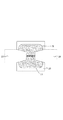
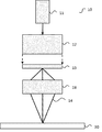
- FIG. 2 is a view showing an example of the configuration of a laser irradiation apparatus 10;
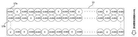
- FIG. 2 is a view showing an example of the configuration of a microlens array 13; It is a schematic diagram which shows the example of the thin-film transistor 20 by which the predetermined area
- FIG. FIG. 7 is a view showing another configuration example of the microlens array 13;
- FIG. 7 is a table showing an example of correspondences regarding a plurality of microlenses 17 included in the microlens array 13.
- FIG. 7 is a view showing another configuration example of the microlens array 13;
- FIG. 2 is a view showing an example of the configuration of a microlens array 13 and a projection mask pattern 15;
- FIG. 16 is a table showing another example of the correspondence relationship between the plurality of microlenses 17 included in the microlens array 13;
- FIG. 16 is a table showing another example of the correspondence relationship between the plurality of microlenses 17 included in the microlens array 13;
- FIG. FIG. 6 is a view showing another configuration example of the laser irradiation device 10;
- FIG. 1 is a view showing an example of the arrangement of a laser irradiation apparatus 10 according to the first embodiment of the present invention.
- the laser irradiation device 10 performs, for example, annealing treatment by irradiating the channel region formation planned region with laser light. It is an apparatus for polycrystallizing a channel region formation scheduled region.
- the laser irradiation device 10 is used, for example, when forming a thin film transistor of a pixel such as a peripheral circuit of a liquid crystal display device.
- a gate electrode made of a metal film such as Al is patterned on the substrate 30 by sputtering.
- a gate insulating film made of a SiN film is formed on the entire surface of the substrate 30 by low temperature plasma CVD.
- an amorphous silicon thin film 21 is formed on the gate insulating film, for example, by plasma CVD. That is, the amorphous silicon thin film 21 is formed (deposited) on the entire surface of the substrate 30.
- a silicon dioxide (SiO 2 ) film is formed on the amorphous silicon thin film 21.
- the laser irradiation device 10 illustrated in FIG. 1 applies a laser beam 14 to a predetermined region (a region to be a channel region in the thin film transistor 20) on the gate electrode of the amorphous silicon thin film 21 to perform annealing treatment.
- the region is polycrystallized and polysiliconized.
- the substrate 30 is, for example, a glass substrate, but the substrate 30 is not necessarily a glass material, and may be a substrate of any material such as a resin substrate formed of a material such as a resin.
- the beam system of the laser light 14 emitted from the laser light source 11 is expanded by the coupling optical system 12, and the luminance distribution is made uniform.
- the laser light source 11 is an excimer laser which emits, for example, laser light 14 having a wavelength of 308 nm or 248 nm at a predetermined repetition cycle.
- the laser beam 14 is separated into a plurality of laser beams 14 by a plurality of openings (transmission regions) of a projection mask pattern 15 (not shown) provided on the microlens array 13, and a predetermined amount of amorphous silicon thin film 21 is obtained. It is irradiated to the area of The microlens array 13 is provided with a projection mask pattern 15, and the projection mask pattern 15 irradiates a predetermined area with the laser light 14. Then, a predetermined region of the amorphous silicon thin film 21 is instantaneously heated and melted, and a part of the amorphous silicon thin film 21 becomes a polysilicon thin film 22.
- the projection mask pattern 15 may be called a projection mask.
- the polysilicon thin film 22 has electron mobility higher than that of the amorphous silicon thin film 21 and is used in the thin film transistor 20 as a channel region for electrically connecting the source 23 and the drain 24.
- the example using the micro lens array 13 is shown, it is not necessary to necessarily use the micro lens array 13, and the laser beam 14 may be irradiated using one projection lens. .
- the case where the polysilicon thin film 22 is formed using the microlens array 13 will be described as an example.
- FIG. 2 is a view showing a configuration example of the microlens array 13 used for the annealing process.
- the microlens array 13 As shown in FIG. 2, in the microlens array 13, twenty microlenses 17 are disposed in one column (or one row) in the scanning direction.
- the laser irradiation apparatus 1 uses at least a portion of the twenty microlenses 17 included in one column (or one row) of the microlens array 13 with respect to a predetermined region of the amorphous silicon thin film 21 to form a laser beam 14. Irradiate.
- the number of microlenses 17 in one column (or one row) included in the microlens array 13 is not limited to 20, but may be any number.
- the microlens array 13 includes twenty microlenses 17 in one column (or row), but includes, for example, 165 microlenses 17 in one row (or one column). Needless to say, one hundred sixty-five is an example, and any number may be used.
- FIG. 3 is a schematic view showing an example of the thin film transistor 20 in which a predetermined region is annealed.
- the thin film transistor 20 is formed by first forming the polysilicon thin film 22 and then forming the source 23 and the drain 24 at both ends of the formed polysilicon thin film 22.
- a polysilicon thin film 22 is formed between the source 23 and the drain 24.
- the laser irradiation apparatus 10 uses, for example, twenty microlenses 17 included in one column (or one row) of the microlens array 13 shown in FIG. 3 with respect to a predetermined region of the amorphous silicon thin film 21. Irradiate. That is, the laser irradiation apparatus 10 irradiates 20 shots of laser light 14 to a predetermined region of the amorphous silicon thin film 21. As a result, in the region to be the thin film transistor 20, the predetermined region of the amorphous silicon thin film 21 is instantaneously heated and melted to form the polysilicon thin film 22.
- FIG. 4 is a schematic view showing an example of the substrate 30 on which the laser irradiation apparatus 10 irradiates the laser light 14.
- the substrate 30 is not necessarily a glass material, and may be a substrate of any material such as a resin substrate formed of a material such as a resin.
- the substrate 30 includes a plurality of pixels 31, and each of the pixels 31 includes a thin film transistor 20.
- the thin film transistor 20 executes transmission control of light in each of the plurality of pixels 31 by electrically turning ON / OFF.
- An amorphous silicon thin film 21 is provided on the entire surface of the substrate 30.
- the predetermined region of the amorphous silicon thin film 21 is a portion to be a channel region of the thin film transistor 20.
- the laser irradiation apparatus 10 irradiates a predetermined region (a region to be a channel region in the thin film transistor 20) of the amorphous silicon thin film 21 with the laser light.
- the laser irradiation device 10 irradiates the laser light 14 with a predetermined cycle, moves the substrate 30 during the time when the laser light 14 is not irradiated, and the laser light 14 is moved to a predetermined region of the next amorphous silicon thin film 21.
- the amorphous silicon thin film 21 is disposed on the entire surface of the substrate 30.
- the laser irradiation apparatus 10 irradiates the laser light 14 to a predetermined region of the amorphous silicon thin film 21 disposed on the substrate 30 at a predetermined cycle.
- the laser irradiation apparatus 10 irradiates the laser light 14 to a predetermined region of the amorphous silicon thin film 21 on the substrate using the microlens array 13.
- the laser irradiation apparatus 10 irradiates, for example, the region A of the amorphous silicon thin film 21 provided (deposited) on the entire surface of the substrate 30 as shown in FIG.
- the laser irradiation apparatus 10 also irradiates the laser beam 14 to the region B shown in FIG. 4 of the amorphous silicon thin film 21 provided (deposited) on the entire surface of the substrate 30.
- the laser irradiation apparatus 10 irradiates the laser beam 14 using each of the twenty microlenses 17 included in one row (or one row) of the microlens array 13 shown in FIG. 2 in order to perform the annealing process. It is possible to do.
- the region A in FIG. 4 of the amorphous silicon thin film 21 provided (deposited) on the entire surface of the substrate 30 is, first, the first micro of the row A of the microlens array 13 shown in FIG.
- the laser beam 14 is irradiated using the lens 17.
- the substrate 30 is moved by a predetermined interval "H".
- the laser irradiation apparatus 10 may stop the irradiation of the laser light 14.
- the region A of FIG. 4 in the amorphous silicon thin film 21 uses the second microlenses 17 of the B row of the microlens array 13 shown in FIG. It is irradiated with 14.
- the laser irradiation apparatus 10 may stop the irradiation of the laser beam 14 while the substrate 30 is moving, or may irradiate the laser beam 14 to the substrate 30 which is moving continuously.
- the irradiation head (that is, the laser light source 11, the coupling optical system 12, the microlens array 13, and the projection mask pattern 15) of the laser irradiation apparatus 10 may move relative to the substrate 30.
- the laser irradiation apparatus 10 repeatedly executes this, and finally, with respect to the region A of FIG. 4 in the amorphous silicon thin film 21, the microlenses 17 of T rows of the microlens array 13 shown in FIG.
- the laser beam 14 is irradiated using the micro lens 17) of
- the region A of the amorphous silicon thin film 21 is irradiated with the laser beam 14 using each of the twenty microlenses 17 included in one row (or one row) of the microlens array 13 shown in FIG. become.
- the laser irradiation apparatus 10 also applies to the region B in FIG. 4 of the amorphous silicon thin film 21 of the twenty microlenses 17 included in one column (or one row) of the microlens array 13 shown in FIG. Each is used to emit a laser beam 14.
- the region B is different in position by “H” in the moving direction of the substrate 30 compared to the region A, the timing at which the laser light 14 is irradiated is delayed by one irradiation. That is, when the region A is irradiated with the laser beam 14 using the second microlens 17 in the B row in FIG. 2, the region B uses the first microlens 17 in the A row in FIG. 14 is irradiated.
- the region A is irradiated with the laser light 14 using the twentieth microlens 17 (ie, the last microlens 17) of the T row in FIG.
- Laser light is emitted using the lens 17.
- the region B laser light is emitted using the micro-lenses 17 of the T-row (that is, the last micro-lenses 17) at the next irradiation timing of the laser light.
- the projection magnification for each of the plurality of microlenses 17 is (The projection magnification of the laser beam 14 on the substrate 30) may be different.
- the projection magnification is different, the energy density of the laser beam irradiated to the substrate 30 varies, which causes the result of the annealing process to vary.
- the electron mobility of the polysilicon thin film formed on the substrate 30 also varies, and as a result, the characteristic of the thin film transistor 20 varies.
- the projection magnification of each of the plurality of microlenses 17 included in the microlens array 13 is measured, and a plurality of projection magnifications among the measured projection magnifications are used.
- the transmittance of each of the laser beams 14 of the microlenses 17 is adjusted.
- the laser beams 14 irradiated by each of the plurality of microlenses 17 have substantially the same energy density on the substrate.
- the electron mobility of the polysilicon thin film formed by the laser beam 14 irradiated by each of the plurality of microlenses 17 is also substantially the same, which makes it possible to reduce the variation in the characteristics of the thin film transistor 20.
- the transmittance of the opening (transmission region) of the corresponding projection mask pattern 15 is set.
- the other microlenses 17 may be used. Adjust the transmittance of For example, the transmittance of the other microlens 17 is set in accordance with the transmittance of the microlens 17 having the largest projection magnification being 100%.
- the transmittance of the microlens 17 having the largest projection magnification is not necessarily 100%, and may be less than 100%.
- FIG. 5 is a schematic view showing projection magnifications of the plurality of microlenses 17 included in the microlens array 13.
- the projection magnification is shown by increase and decrease from the predetermined value with reference to the predetermined value.
- the microlenses 17 have projection magnifications different from one another.
- the projection magnification of the microlens 17a is "+ 0.001%”
- the projection magnification of the microlens 17b is "-0.005%”.
- each of the microlenses 17 included in the microlens array 13 has different projection magnifications.
- the projection magnification is a projection magnification when the laser beam 14 transmitted through each of the plurality of microlenses 17 is projected onto the substrate 30.
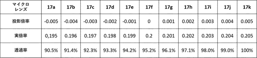
- FIG. 6 is a table showing the correspondence between the projection magnification of the microlens 17, the actual projection magnification, and the transmittance set to the opening of the projection mask pattern 15.
- the transmittance of the microlens 17 k having the lowest projection magnification is set to be 100%.
- the transmittance of the laser beam 14 from the microlens 17 K is Set “100%”.
- the transmittance of laser light from the other microlens 17 is set to the other microlens 17 based on the projection magnification of the microlens 17 k having a transmittance of 100%.
- the microlens 17a whose projection magnification is "-0.005" (the actual projection magnification is "0.195") is the projection magnification "0.005" of the microlens 17k (the actual projection magnification is "0. 0").
- the transmittance is set to" 90.5% ".
- the transmittance is set to" 91.4% ".
- the transmittances of the other microlenses c to j are similarly set.
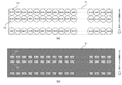
- FIG. 7 is a diagram showing the state of transmittance set for each of the microlenses 17 included in the microlens array 13 based on the correspondence illustrated in FIG.
- the microlens array 13 shown in FIG. 7A is the same as the microlens array 13 shown in FIG. As illustrated in FIG. 7A, the projection magnifications of the plurality of microlenses 17 included in the microlens array 13 are different from one another. Therefore, the transmittance of each of the plurality of microlenses 17 (the transmittance of the opening (transmission region) of the projection mask pattern 15) is shown in FIG. 7B based on the correspondence illustrated in FIG. Set
- the transmittance is set to "96.1%”. Further, since the microlens 17 b has a projection magnification of “ ⁇ 0.005”, the transmittance is set to “90.5%”. The transmittances of the other microlenses 17 are similarly set based on the projection magnification.
- the transmittance of each of the plurality of microlenses 17 (that is, the transmittance of the opening (transmission region) of the projection mask pattern 15) is set so that the energy density of the laser beam 14 on the substrate is substantially the same. It will be done. Specifically, the transmittance of each of the microlenses 17 is controlled so that all the microlenses 17 included in the microlens array 13 have substantially the same energy density on the substrate of the microlenses 17 with the lowest projection magnification. Is set.
- FIG. 8 is a view for explaining the transmittance of the opening 16 of the projection mask pattern 15 in the first embodiment of the present invention.
- the transmittance of each of the plurality of openings 16 included in the projection mask pattern 15 is set such that the laser light 14 is transmitted with the transmittance set in the corresponding microlens 17. Be done.
- the opening 16 a corresponds to the microlens 17 a whose transmittance is set to “96.1%”, so the transmittance of the laser light 14 of the opening 16 a is set to “96.1%”. Be done.
- the transmittance of the laser beam 14 of the opening 16 b is set to “90.5%”.
- the transmittance of each of the plurality of openings 16 included in the projection mask pattern 15 is the transmittance set for the corresponding microlens 17.
- the total transmittance (total value of transmittances) of the twenty openings 16 in one line of the projection mask pattern 15 is set to a predetermined value (a predetermined area). That is, the total transmittance of the openings 16 in each row of the projection mask pattern 15 illustrated in FIG. 8B is set to a predetermined value (predetermined transmittance).
- predetermined transmittance a predetermined value
- the total transmittance of the twenty openings 16 in one row of the projection mask pattern 15 does not necessarily have to be set to a predetermined value (predetermined transmittance), and the total transmittance of the laser beam 14 is “row May differ depending on
- the opening (transmission region) 16 of the projection mask pattern 15 is provided to be orthogonal to the moving direction (scanning direction) of the substrate 30.
- the opening (transmission region) 16 of the projection mask pattern 15 does not have to be orthogonal to the moving direction (scanning direction) of the substrate 30, and is parallel (substantially parallel) to the moving direction (scanning direction). May be provided.
- the substrate 30 moves by a predetermined distance each time the laser beam 14 is irradiated to the microlens array 13.
- the predetermined distance is the distance “H” between the plurality of thin film transistors 20 on the substrate 30.
- the laser irradiation apparatus 10 stops the irradiation of the laser beam 14 while moving the substrate 30 by the predetermined distance.
- the laser irradiation apparatus 10 irradiates the laser light 14 again using the microlenses 17 included in the microlens array 13.
- the laser beam 14 is irradiated to one amorphous silicon thin film 21 by twenty microlenses 17 because the microlens array 13 shown in FIG. 2 is used.
- the source 23 and the drain 24 are formed in the thin film transistor 20.
- the transmittance of each of the plurality of microlenses 17 is set so that the energy density of the laser beam 14 on the substrate is substantially the same. Therefore, the variation of the projection magnification of each of the plurality of microlenses 17 is It is possible to reduce the variation in the energy density irradiated onto the substrate 30 due to the above. Since the energy density of the laser beam 14 is substantially the same, the variation in electron mobility of the polysilicon thin film formed using the laser beam 14 is reduced. As a result, variations in the characteristics of the plurality of thin film transistors on the substrate can be reduced.
- the second embodiment of the present invention is an embodiment in which the size of the opening 16 of the projection mask pattern 15 is set based on the projection magnification of the microlens 17.
- FIG. 9 shows the correspondence between “projection magnification of micro lens 17”, “actual projection magnification”, and “size of opening 16 of projection mask pattern 15” in the second embodiment of the present invention.
- Is a table showing The opening 16 is substantially rectangular, and the “size of the opening 16 of the projection mask pattern 15” is indicated by the length (Y direction) and the width (X direction).
- the openings 16 do not necessarily have to be substantially rectangular, and in that case, the “size of the openings 16 of the projection mask pattern 15” may be indicated by an area or the like.
- each of the plurality of microlenses 17 included in the microlens array 13 has a certain variation, and the variation in the lens curvature is caused by the variation.
- the projection magnification projection magnification of the laser beam 14 on the substrate 30
- the projection magnification may be different for each of the plurality of microlenses 17. Therefore, if the sizes of the openings 16 of the projection mask pattern 15 are substantially the same, the range in which the laser annealing process is performed on the substrate 30 is different for each microlens 17 because the projection magnifications are different.
- the electron mobility of the polysilicon thin film formed on the substrate 30 varies, which causes a problem that the characteristics of the thin film transistor 20 vary.
- the projection magnification of each of the plurality of microlenses 17 included in the microlens array 13 is measured, and the opening 16 of the projection mask pattern 15 is based on the measured projection magnification. Adjust the size of As a result, the range to be subjected to the laser annealing process by the laser beam 14 transmitted through each of the plurality of microlenses 17 becomes substantially the same, whereby the variation in the characteristics of the thin film transistor 20 can be reduced.
- the microlenses 17f having a projection magnification of “0” (actual projection magnification is “0.2”)
- the size of the opening 16 is set to “100 ( ⁇ m)” in the vertical (Y direction) and “47.5 ( ⁇ m)” in the width (X direction). That is, based on the case where the projection magnification is a predetermined value, the “size of the opening 16 of the projection mask pattern 15” in that case is “100 ( ⁇ m)” and the width (X direction) “47 And set “5 ( ⁇ m)”.
- the actual projection magnification is “0.2”
- the length (Y direction) is “20 ( ⁇ m)”
- the width (X direction) is “9.5 ( ⁇ m) on the substrate 30.
- Laser annealing is performed in the range of
- the transmittance of laser light from the other microlens 17 is set to the other microlens 17 based on the projection magnification of the microlens 17 k having a transmittance of 100%.
- the microlens 17 a having a projection magnification of “ ⁇ 0.005” can be used to “size the opening 16 of the projection mask pattern 15” in the vertical direction (Y direction). Is set as “102.56 ( ⁇ m)” and the width (X direction) as “48.72 ( ⁇ m)”.
- the microlens 17 b has a projection magnification of “ ⁇ 0.004” (actual projection magnification is “0.196”)
- “the size of the opening 16 of the projection mask pattern 15” The direction is set to "102.04 ( ⁇ m)” and the width (X direction) to "47.98 ( ⁇ m)”.
- “the size of the opening 16 of the projection mask pattern 15” is set for the other microlenses 17c to j.
- each of the respective microlenses 17 has the corresponding relationship illustrated in FIG.
- the size of the opening 16 corresponding to the micro lens 17 is adjusted.
- the projection magnification of the microlens 17 a in FIG. 5 is “+0.001” (the actual projection magnification is “0.201”)
- the size of the opening 16 corresponding to the microlens 17 a is The Y direction is set to "99.50 (.mu.m)" and the width (X direction) to "47.26 (.mu.m)".
- the size of the opening 16 corresponding to the microlens 17 b is “102.56 ( ⁇ m) in the longitudinal direction (Y direction)
- the width (X direction) is set to “48.72 ( ⁇ m)”.
- the size of the opening 16 corresponding to the plurality of microlenses 17 included in the microlens array 13 is adjusted.
- each of the openings 16 of the projection mask pattern 15 has a size based on the projection magnification of the corresponding microlens 17, the range to be subjected to the laser annealing process by the laser beam 14 transmitted through the microlens 17 is It becomes almost the same.
- the laser annealing process is performed by the laser beam 14 which transmits each of the plurality of microlenses 17.
- the ranges become substantially the same, which makes it possible to reduce variations in the characteristics of the thin film transistor 20.
- the transmittance of each of the plurality of microlenses 17 (first embodiment) and the size of the opening 16 of the projection mask pattern 15 are determined based on the projection magnification of the microlens 17. (Second embodiment) is set.
- FIG. 10 shows the “projection magnification of the micro lens 17”, the “actual projection magnification”, the “transmittance set in the opening of the projection mask pattern 15”, and the “projection” in the third embodiment of the present invention. It is a table
- the relationship between “the projection magnification of the micro lens 17”, “the actual projection magnification”, and “the transmittance set to the opening of the projection mask pattern 15” is the same as the correspondence illustrated in FIG. Detailed description will be omitted as it is.
- the relationship between “the projection magnification of the micro lens 17”, “the actual projection magnification”, and “the size of the opening 16 of the projection mask pattern 15” is the same as the correspondence illustrated in FIG. Therefore, the detailed description is omitted.
- the transmittance to be set to the opening of the projection mask pattern 15 is set based on the projection magnification of the microlens 17 based on the correspondence illustrated in FIG.
- the size of the opening 16 of the mask pattern 15 is also set.
- the laser beam 14 transmitted through the projection mask pattern 15 is laser-annealed by the laser beam 14 transmitted through each of the plurality of microlenses 17 in addition to the energy density becoming substantially the same on the substrate 30. Since the ranges of the characteristics are substantially the same, variations in the characteristics of the thin film transistor 20 can be reduced.
- each of the plurality of microlenses 17 has the corresponding relationship illustrated in FIG.
- the size of the opening 16 corresponding to the micro lens 17 is adjusted. For example, since the projection magnification of the microlens 17 a in FIG. 5 is “+0.001” (the actual projection magnification is “0.201”), the transmittance of the laser beam 14 in the opening 16 a is “96.1%.
- the size of the opening 16 corresponding to the microlens 17 a is “99.50 ( ⁇ m)” in the vertical (Y direction) and “47.26 (width in the X direction)”. ⁇ m) is set.
- the transmittance of the laser beam 14 at the opening 16 b is set to “90.5%”
- the microlens The size of the opening 16 corresponding to 17 b is set to “102.56 ( ⁇ m)” in the vertical (Y direction) and “48.72 ( ⁇ m)” in the width (X direction).
- the transmittance of the opening 16 corresponding to the plurality of microlenses 17 included in the microlens array 13 and the size of the opening 16 are adjusted.
- each of the openings 16 of the projection mask pattern 15 has a transmittance such that the energy density is substantially the same on the substrate 30, and has a size based on the projection magnification of the corresponding microlens 17
- the energy density of the laser beam 14 transmitted through the micro lens 17 is substantially the same, and the ranges to be subjected to the laser annealing process are substantially the same.
- the transmittance of each of the plurality of microlenses 17 that is, the transmittance of the opening (transmission region) of the projection mask pattern 15
- the energy density on the substrate is set to be substantially the same
- the size of the opening 16 of the projection mask pattern 15 is adjusted based on the projection magnification.
- the laser beam 14 transmitted through the projection mask pattern 15 is laser-annealed by the laser beam 14 transmitted through each of the plurality of microlenses 17 in addition to the energy density becoming substantially the same on the substrate 30. Since the ranges of the characteristics are substantially the same, variations in the characteristics of the thin film transistor 20 can be reduced.
- the fourth embodiment of the present invention is an embodiment in which laser annealing is performed using one projection lens 18 instead of the microlens array 13.
- the projection magnification of the peripheral portion may be different from that of the central portion due to the influence of aberration and the like.
- the energy density of the laser beam irradiated to the substrate 30 varies, which causes the result of the annealing process to vary.
- the projection magnification is different, so that the range of the substrate 30 subjected to the laser annealing is the central portion or the peripheral portion of the projection lens 18. It will be different. As a result, the electron mobility of the polysilicon thin film formed on the substrate 30 varies, which causes a problem that the characteristics of the thin film transistor 20 vary.
- uniform transmittance is realized by changing the transmittance of the opening 16 of the projection mask pattern 15 provided on a single projection lens 18. For example, when the projection magnification of the peripheral part is smaller than that of the central part in a single projection lens, the transmittance of “the opening 16 at the central part of the projection mask pattern 15” corresponding to the central part of the projection lens
- the projection mask pattern is set by setting the transmittance of the “opening 16 at the periphery of the projection mask pattern 15” corresponding to the periphery of the projection lens lower than that of the center It becomes possible to realize uniform illumination over the entire 15.
- the projection magnification is measured at each of the predetermined portions of the single projection lens 18, and the size of the opening 16 of the projection mask pattern 15 is adjusted based on the measured projection magnification.
- the range to be laser-annealed by the laser beam 14 transmitted through each of the predetermined portions of the single projection lens 18 becomes substantially the same, thereby making it possible to reduce the variation in the characteristics of the thin film transistor 20. Become.
- (1) changing the transmittance of the opening 16 of the projection mask pattern 15 and (2) adjusting the size of the opening 16 of the projection mask pattern 15 can be performed either. Either one or the other may be performed.
- FIG. 11 is a view showing an example of the configuration of a laser irradiation apparatus 10 according to the fourth embodiment of the present invention.
- the laser irradiation apparatus 10 in the fourth embodiment of the present invention includes a laser light source 11, a coupling optical system 12, a projection mask pattern 15, and a projection lens 18.
- the laser light source 11 and the coupling optical system 12 have the same configuration as the laser light source 11 and the coupling optical system 12 in the first embodiment of the present invention shown in FIG. It is omitted.
- the projection mask pattern has the same configuration as the projection mask pattern in the first embodiment of the present invention, the detailed description will be omitted.
- the laser light passes through the opening (transmission region) of the projection mask pattern 15 (not shown), and is irradiated onto a predetermined region of the amorphous silicon thin film 21 by the projection lens 18.
- a predetermined region of the amorphous silicon thin film 21 is instantaneously heated and melted, and a part of the amorphous silicon thin film 21 becomes the polysilicon thin film 22.
- the laser irradiation apparatus 10 irradiates the laser light 14 with a predetermined cycle, moves the substrate 30 during the time when the laser light 14 is not irradiated, and the next amorphous silicon thin film 21 is formed.
- the laser beam 14 is irradiated to the portion.
- the amorphous silicon thin film 21 is disposed at a predetermined interval “H” in the moving direction. Then, the laser irradiation apparatus 10 irradiates the portion of the amorphous silicon thin film 21 disposed on the substrate 30 with the laser light 14 at a predetermined cycle.
- the laser beam 14 is converted by the magnification of the optical system of the projection lens 18. That is, the pattern of the projection mask pattern 15 (the pattern of the opening 16) is converted by the magnification of the optical system of the projection lens 18, and a predetermined region on the substrate 30 is laser annealed.
- the mask pattern (pattern of the opening 16) of the projection mask pattern 15 is converted by the magnification of the optical system of the projection lens 18, and a predetermined region on the substrate 30 is laser annealed.
- the magnification of the optical system of the projection lens 18 is about twice
- the mask pattern of the projection mask pattern 15 is multiplied by about 1/2 (0.5) and the predetermined region of the substrate 30 is laser annealed .
- the magnification of the optical system of the projection lens 18 is not limited to about twice, and may be any magnification.
- the mask pattern of the projection mask pattern 15 is laser-annealed in a predetermined region on the substrate 30 in accordance with the magnification of the optical system of the projection lens 18. For example, if the magnification of the optical system of the projection lens 18 is four times, the mask pattern (pattern of the opening 16) of the projection mask pattern 15 is multiplied by about 1/4 (0.25) and The area is laser annealed.
- the reduced image of the projection mask pattern 15 irradiated to the substrate 30 is a pattern rotated 180 degrees around the optical axis of the lens of the projection lens 18.
- the projection lens 18 forms an erect image
- the reduced image of the projection mask pattern 15 irradiated onto the substrate 30 is the projection mask pattern 15 as it is.
- the projection magnification of the peripheral part may be different compared to the central part under the influence of aberration etc.
- the substrate 30 is irradiated.
- the energy density of the laser light varies, which causes the results of the annealing process to vary.
- the electron mobility of the polysilicon thin film formed on the substrate 30 also varies, and as a result, the characteristic of the thin film transistor 20 varies.
- the projection magnification is measured by dividing the projection lens 18 into predetermined portions, such as the central portion and the peripheral portion of the projection lens 18, and the projection magnification is measured.
- the transmittance of the laser beam 14 of each of the other portions is adjusted based on the portion (for example, the peripheral portion of one) of the lowest projection magnification.
- the transmittance of the laser beam 14 the laser beams 14 irradiated by each of the predetermined portions of the projection lens 18 have substantially the same energy density on the substrate.
- the electron mobility of the polysilicon thin film formed by the laser beam 14 irradiated by the projection lens 18 is also substantially the same, whereby the variation in the characteristics of the thin film transistor 20 can be reduced.
- the transmittance of the other portion is adjusted in accordance with the portion where the projection magnification is the largest (that is, the lowest transmittance).
- the transmittance of the other portion is set in accordance with the transmittance of one portion having the largest projection magnification being 100%.
- the transmittance of one portion having the largest projection magnification is not necessarily 100%, and may be less than 100%.
- the size of the openings 16 of the projection mask pattern 15 are substantially the same, the area to be subjected to the laser annealing process on the substrate 30 is different for each of the predetermined portions of the projection lens 18 because the projection magnifications are different. It will be different. As a result, the electron mobility of the polysilicon thin film formed on the substrate 30 varies, which causes a problem that the characteristics of the thin film transistor 20 vary.
- the projection magnification of each of the predetermined portions of the single projection lens 18 is measured, and the size of the opening 16 of the projection mask pattern 15 is determined based on the measured projection magnification. Adjust the As a result, the range to be laser-annealed by the laser beam 14 transmitted through each of the predetermined portions of the single projection lens 18 becomes substantially the same, thereby making it possible to reduce the variation in the characteristics of the thin film transistor 20. Become.
- the transmittance of each of the predetermined portions of the single projection lens 18 ie, the transmittance of the opening (transmission region) of the projection mask pattern 15
- the size of the opening 16 of the projection mask pattern 15 is adjusted based on the projection magnification.
- (1) changing the transmittance of the opening 16 of the projection mask pattern 15 and (2) adjusting the size of the opening 16 of the projection mask pattern 15 Either one or the other may be performed.
Landscapes
- Physics & Mathematics (AREA)
- Optics & Photonics (AREA)
- Engineering & Computer Science (AREA)
- General Physics & Mathematics (AREA)
- Plasma & Fusion (AREA)
- Mechanical Engineering (AREA)
- Chemical & Material Sciences (AREA)
- Chemical Kinetics & Catalysis (AREA)
- General Chemical & Material Sciences (AREA)
- Oil, Petroleum & Natural Gas (AREA)
- Recrystallisation Techniques (AREA)
- Thin Film Transistor (AREA)
- Electromagnetism (AREA)
- Health & Medical Sciences (AREA)
- Toxicology (AREA)
Abstract
本発明の一実施形態におけるレーザ照射装置は、レーザ光を発生する光源と、基板上に被着されたアモルファスシリコン薄膜の所定の領域に、前記レーザ光を照射する投影レンズと、前記投影レンズ上に設けられ、前記アモルファスシリコン薄膜の所定の領域に対して前記レーザ光が照射されるように、複数の開口部が設けられた投影マスクパターンと、を備え、前記複数の開口部の各々は、前記投影レンズの投影倍率に基づく透過率を有することを特徴とする。
Description
本発明は、薄膜トランジスタの形成に関するものであり、特に、アモルファスシリコン薄膜にレーザ光を照射して、ポリシリコン薄膜を形成するためのレーザ照射装置、レーザ照射方法及び投影マスクに関する。
逆スタガ構造の薄膜トランジスタとして、アモルファスシリコン薄膜をチャネル領域に使用したものが存在する。ただ、アモルファスシリコン薄膜は電子移動度が小さいため、当該アモルファスシリコン薄膜をチャネル領域に使用すると、薄膜トランジスタにおける電荷の移動度が小さくなるという難点があった。
そこで、アモルファスシリコン薄膜の所定の領域をレーザ光により瞬間的に加熱することで多結晶化し、電子移動度の高いポリシリコン薄膜を形成して、当該ポリシリコン薄膜をチャネル領域に使用する技術が存在する。
例えば、特許文献1には、基板にアモルファスシリコン薄膜を形成し、その後、このアモルファスシリコン薄膜にエキシマレーザ等のレーザ光を照射してレーザアニールすることにより、短時間での溶融凝固によって、ポリシリコン薄膜に結晶化させる処理を行うことが開示されている。特許文献1には、当該処理を行うことにより、薄膜トランジスタのソースとドレイン間のチャネル領域を、電子移動度の高いポリシリコン薄膜とすることが可能となり、トランジスタ動作の高速化が可能になる旨が記載されている。
ここで、特許文献1には、レーザ光をマイクロレンズアレイに含まれる複数のマイクロレンズを透過させて、1回のレーザ光の照射により、基板上の複数個所をレーザアニールすることが記載されている。しかしながら、マイクロレンズアレイに含まれる複数のマイクロレンズの各々は、その形状が互いに異なっている場合がある。そのため、複数のマイクロレンズを透過するレーザ光のエネルギ密度は、互いにばらつきが生じる場合が生じ、当該レーザ光を用いて形成されるポリシリコン薄膜の電子移動度にもばらつきが生じるおそれがある。薄膜トランジスタの特性は電子移動密度に依存するため、複数のマイクロレンズの各々を透過するレーザ光のエネルギ密度にばらつきがあることにより、基板上の複数の薄膜トランジスタの特性にばらつきが生じてしまうという問題が生じる。
本発明の目的は、かかる問題点に鑑みてなされたものであって、基板に含まれる複数の薄膜トランジスタの特性のばらつきを抑制可能なレーザ照射装置、レーザ照射方法及び投影マスクを提供することである。
本発明の一実施形態におけるレーザ照射装置は、レーザ光を発生する光源と、基板上に被着されたアモルファスシリコン薄膜の所定の領域に、前記レーザ光を照射する投影レンズと、前記投影レンズ上に設けられ、前記アモルファスシリコン薄膜の所定の領域に対して前記レーザ光が照射されるように、複数の開口部が設けられた投影マスクパターンと、を備え、前記複数の開口部の各々は、前記投影レンズの投影倍率に基づく透過率を有することを特徴とする。
本発明の一実施形態におけるレーザ照射装置において、前記投影レンズは、前記レーザ光を分離可能なマイクロレンズアレイに含まれる複数のマイクロレンズであり、前記複数の開口部の各々は、前記マイクロレンズの投影倍率に基づく透過率を有することを特徴としてもよい。
本発明の一実施形態におけるレーザ照射装置において、前記複数の開口部の各々は、前記複数のマイクロレンズの各々の投影倍率のうちの最大値と、前記マイクロレンズの投影倍率との差異に基づいて決定された透過率を有することを特徴としてもよい。
本発明の一実施形態におけるレーザ照射装置において、前記複数のマイクロレンズのうち、前記投影倍率が最大値となる一のマイクロレンズの透過率は、予め定められた透過率であり、前記複数のマイクロレンズのうちの他のマイクロレンズは、前記予め定められた透過率と、前記最大値と前記他のマイクロレンズの投影倍率との差異に基づいて決定された透過率を有する、ことを特徴としてもよい。
本発明の一実施形態におけるレーザ照射装置において、前記複数の開口部の各々は、前記複数のマイクロレンズの各々の投影倍率に基づいて決定された大きさであることを特徴としてもよい。
本発明の一実施形態におけるレーザ照射装置において、前記複数の開口部の各々は長方形状であり、前記複数のマイクロレンズの各々の投影倍率に基づいて前記長方形状の長さ及び幅が決定されることを特徴としてもよい。
本発明の一実施形態におけるレーザ照射装置において、前記投影レンズは、薄膜トランジスタに含まれるソース電極とドレイン電極との間に対応する領域に被着されたアモルファスシリコン薄膜にレーザ光を照射して、ポリシリコン薄膜を形成することを特徴としてもよい。
本発明の一実施形態におけるレーザ照射方法は、レーザ光を発生する第1のステップと、基板上に被着されたアモルファスシリコン薄膜の所定の領域に、複数の開口部を含む投影マスクパターンが設けられた投影レンズを用いて、前記レーザ光を照射する第2のステップと、前記レーザ光が照射されるごとに、前記基板を所定の方向に移動する第3のステップと、を含み、前記複数の開口部の各々は、前記投影レンズの投影倍率に基づく透過率を有することを特徴とする。
本発明の一実施形態におけるレーザ照射方法において、前記投影レンズは、前記レーザ光を分離可能なマイクロレンズアレイに含まれる複数のマイクロレンズであり、前記複数の開口部の各々は、前記マイクロレンズの投影倍率に基づく透過率を有することを特徴としてもよい。
本発明の一実施形態におけるレーザ照射方法において、前記複数の開口部の各々は、前記複数のマイクロレンズの各々の投影倍率のうちの最大値と、前記マイクロレンズの投影倍率との差異に基づいて決定された透過率を有することを特徴としてもよい。
本発明の一実施形態におけるレーザ照射方法において、前記複数の開口部の各々は、前記複数のマイクロレンズの各々の投影倍率に基づいて決定された大きさであることを特徴としてもよい。
本発明の一実施形態における投影マスクは、光源から発生されたレーザ光を照射する投影レンズ上に配置される投影マスクであって、前記投影マスクは、所定の方向に移動する基板に被着されたアモルファスシリコン薄膜の所定の領域に対して前記レーザ光が照射されるように複数の開口部が設けられ、前記複数の開口部の各々は、前記投影レンズの投影倍率に基づく透過率を有することを特徴とする。
本発明の一実施形態における投影マスクにおいて、前記投影レンズは、前記レーザ光を分離可能なマイクロレンズアレイに含まれる複数のマイクロレンズであり、前記複数の開口部の各々は、前記マイクロレンズの投影倍率に基づく透過率を有することを特徴としてもよい。
本発明の一実施形態における投影マスクにおいて、前記複数の開口部の各々は、前記複数のマイクロレンズの各々の投影倍率のうちの最大値と、前記マイクロレンズの投影倍率との差異に基づいて決定された透過率を有することを特徴としてもよい。
本発明の一実施形態における投影マスクにおいて、前記複数の開口部の各々は、前記複数のマイクロレンズの各々の投影倍率に基づいて決定された大きさであることを特徴としてもよい。
本発明によれば、基板に含まれる複数の薄膜トランジスタの特性のばらつきを抑制可能な、レーザ照射装置、レーザ照射方法及び投影マスクを提供することである。
以下、本発明の実施形態について、添付の図面を参照して具体的に説明する。
(第1の実施形態)
図1は、本発明の第1の実施形態におけるレーザ照射装置10の構成例を示す図である。
図1は、本発明の第1の実施形態におけるレーザ照射装置10の構成例を示す図である。
本発明の第1の実施形態において、レーザ照射装置10は、薄膜トランジスタ(TFT)20のような半導体装置の製造工程において、例えば、チャネル領域形成予定領域にレーザ光を照射してアニール処理し、当該チャネル領域形成予定領域を多結晶化するための装置である。
レーザ照射装置10は、例えば、液晶表示装置の周辺回路などの画素の薄膜トランジスタを形成する際に用いられる。このような薄膜トランジスタを形成する場合、まず、基板30上にAl等の金属膜からなるゲート電極を、スパッタによりパターン形成する。そして、低温プラズマCVD法により、基板30上の全面にSiN膜からなるゲート絶縁膜を形成する。その後、ゲート絶縁膜上に、例えば、プラズマCVD法によりアモルファスシリコン薄膜21を形成する。すなわち、基板30の全面にアモルファスシリコン薄膜21が形成(被着)される。最後に、アモルファスシリコン薄膜21上に二酸化ケイ素(SiO2)膜を形成する。そして、図1に例示するレーザ照射装置10により、アモルファスシリコン薄膜21のゲート電極上の所定の領域(薄膜トランジスタ20においてチャネル領域となる領域)にレーザ光14を照射してアニール処理し、当該所定の領域を多結晶化してポリシリコン化する。なお、基板30は、例えばガラス基板であるが、基板30は必ずしもガラス素材である必要はなく、樹脂などの素材で形成された樹脂基板など、どのような素材の基板であってもよい。
図1に示すように、レーザ照射装置10において、レーザ光源11から出射されたレーザ光14は、カップリング光学系12によりビーム系が拡張され、輝度分布が均一化される。レーザ光源11は、例えば、波長が308nmや248nmなどのレーザ光14を、所定の繰り返し周期で放射するエキシマレーザである。
その後、レーザ光14は、マイクロレンズアレイ13上に設けられた投影マスクパターン15(図示しない)の複数の開口部(透過領域)により、複数のレーザ光14に分離され、アモルファスシリコン薄膜21の所定の領域に照射される。マイクロレンズアレイ13には、投影マスクパターン15が設けられ、当該投影マスクパターン15によって所定の領域にレーザ光14が照射される。そして、アモルファスシリコン薄膜21の所定の領域が瞬間加熱されて溶融し、アモルファスシリコン薄膜21の一部がポリシリコン薄膜22となる。なお、投影マスクパターン15は、投影マスクと呼称されてもよい。
ポリシリコン薄膜22は、アモルファスシリコン薄膜21に比べて電子移動度が高く、薄膜トランジスタ20において、ソース23とドレイン24とを電気的に接続させるチャネル領域に用いられる。なお、図1の例では、マイクロレンズアレイ13を用いた例を示しているが、必ずしもマイクロレンズアレイ13を用いる必要はなく、1個の投影レンズを用いてレーザ光14を照射してもよい。なお、実施形態1では、マイクロレンズアレイ13を用いて、ポリシリコン薄膜22を形成する場合を例にして説明する。
図2は、アニール処理に用いるマイクロレンズアレイ13の構成例を示す図である。図2に示すように、マイクロレンズアレイ13において、スキャン方向の1列(又は1行)には、20個のマイクロレンズ17が配置される。レーザ照射装置1は、アモルファスシリコン薄膜21の所定の領域に対して、マイクロレンズアレイ13の1列(又は1行)に含まれる20個のマイクロレンズ17の少なくとも一部を用いて、レーザ光14を照射する。なお、なお、マイクロレンズアレイ13に含まれる一列(又は一行)のマイクロレンズ17の数は、20個に限られず、いくつであってもよい。
図2に示すように、マイクロレンズアレイ13は、その一列(または一行)にマイクロレンズ17を20個含むが、一行(または一列)には例えば165個含む。なお、165個は例示であって、いくつであってもよいことは言うまでもない。
図3は、所定の領域がアニール処理された薄膜トランジスタ20の例を示す模式図である。なお、薄膜トランジスタ20は、最初にポリシリコン薄膜22を形成し、その後、形成されたポリシリコン薄膜22の両端にソース23とドレイン24を形成することで、作成される。
図3に示すように、薄膜トランジスタ20は、ソース23とドレイン24との間に、ポリシリコン薄膜22が形成されている。レーザ照射装置10は、アモルファスシリコン薄膜21の所定の領域に対して、図3に示したマイクロレンズアレイ13の一列(または一行)に含まれる例えば20個のマイクロレンズ17を用いて、レーザ光14を照射する。すなわち、レーザ照射装置10は、アモルファスシリコン薄膜21の所定の領域に対して、20ショットのレーザ光14を照射する。その結果、薄膜トランジスタ20となる領域において、アモルファスシリコン薄膜21の所定の領域が瞬間加熱されて溶融し、ポリシリコン薄膜22となる。
図4は、レーザ照射装置10がレーザ光14を照射する基板30の例を示す模式図である。なお、基板30は、必ずしもガラス素材である必要はなく、樹脂などの素材で形成された樹脂基板など、どのような素材の基板であってもよい。図4に示すように、基板30は、複数の画素31を含み、当該画素31の各々に薄膜トランジスタ20を備える。薄膜トランジスタ20は、複数の画素31の各々における光の透過制御を、電気的にON/OFFすることにより実行するものである。基板30には、その全面にアモルファスシリコン薄膜21が設けられている。当該アモルファスシリコン薄膜21の所定の領域は、薄膜トランジスタ20のチャネル領域となる部分である。
レーザ照射装置10は、アモルファスシリコン薄膜21の所定の領域(薄膜トランジスタ20においてチャネル領域となる領域)にレーザ光14を照射する。ここで、レーザ照射装置10は所定の周期でレーザ光14を照射し、レーザ光14が照射されていない時間に基板30を移動させ、次のアモルファスシリコン薄膜21の所定の領域に当該レーザ光14が照射されるようにする。図4に示すように、基板30は、その全面にアモルファスシリコン薄膜21が配置される。そして、レーザ照射装置10は、所定の周期で、基板30上に配置されたアモルファスシリコン薄膜21の所定の領域に、レーザ光14を照射する。
そして、レーザ照射装置10は、マイクロレンズアレイ13を用いて、基板上のアモルファスシリコン薄膜21の所定の領域に対して、レーザ光14を照射する。レーザ照射装置10は、例えば、基板30の全面に設けられている(被着している)アモルファスシリコン薄膜21のうち図4に示す領域Aに対して、レーザ光14を照射する。また、レーザ照射装置10は、基板30の全面に設けられている(被着している)アモルファスシリコン薄膜21のうち図4に示す領域Bに対しても、レーザ光14を照射する。
ここで、レーザ照射装置10は、アニール処理を行うために、図2に示すマイクロレンズアレイ13の一列(又は一行)に含まれる20個のマイクロレンズ17の各々を用いて、レーザ光14を照射することが考えられる。
この場合、基板30の全面に設けられている(被着している)アモルファスシリコン薄膜21のうち図4の領域Aは、まず、図2に示すマイクロレンズアレイ13のA列の第1のマイクロレンズ17を用いて、レーザ光14を照射される。その後、基板30を所定の間隔「H」だけ移動させる。基板30が移動している間、レーザ照射装置10は、レーザ光14の照射を停止してもよい。そして、基板30が「H」だけ移動した後、アモルファスシリコン薄膜21のうち図4の領域Aは、図2に示すマイクロレンズアレイ13のB列の第2のマイクロレンズ17を用いて、レーザ光14を照射される。なお、レーザ照射装置10は、基板30が移動している間レーザ光14の照射を停止してもよいし、移動し続けている当該基板30に対してレーザ光14を照射してもよい。
なお、レーザ照射装置10の照射ヘッド(すなわち、レーザ光源11、カップリング光学系12、マイクロレンズアレイ13及び投影マスクパターン15)が、基板30に対して移動してもよい。
レーザ照射装置10は、これを繰り返し実行して、最後に、アモルファスシリコン薄膜21のうち図4の領域Aに対して、図2に示すマイクロレンズアレイ13のT列のマイクロレンズ17(すなわち、最後のマイクロレンズ17)を用いて、レーザ光14を照射する。その結果、アモルファスシリコン薄膜21のうち領域Aは、図2に示すマイクロレンズアレイ13の一列(又は一行)に含まれる20個のマイクロレンズ17の各々を用いて、レーザ光14を照射されることになる。
同様にして、レーザ照射装置10は、アモルファスシリコン薄膜21のうち図4の領域Bに対しても、図2に示すマイクロレンズアレイ13の一列(又は一行)に含まれる20個のマイクロレンズ17の各々を用いて、レーザ光14を照射する。ただ、領域Bは、領域Aに比べて基板30の移動方向に対して「H」だけ位置が異なるため、レーザ光14が照射されるタイミングが、1照射分だけ遅れる。すなわち、領域Aが図2のB列の第2のマイクロレンズ17を用いてレーザ光14を照射される時に、領域Bは、図2のA列の第1のマイクロレンズ17を用いてレーザ光14が照射される。そして、領域Aが図2のT列の第20のマイクロレンズ17(すなわち、最後のマイクロレンズ17)を用いてレーザ光14を照射される時には、領域Bは、一つ前のS列のマイクロレンズ17を用いて、レーザ光が照射されることになる。そして、領域Bは、次のレーザ光の照射のタイミングで、T列のマイクロレンズ17(すなわち、最後のマイクロレンズ17)を用いて、レーザ光が照射されることになる。
ここで、マイクロレンズアレイ13に含まれる複数のマイクロレンズ17の各々は、一定のばらつきを有しており、当該ばらつきによるレンズ曲率のばらつきが生じているため、複数のマイクロレンズ17ごとに投影倍率(基板30上のレーザ光14の投影倍率)が異なる可能性があった。投影倍率が異なると、基板30に照射されるレーザ光のエネルギ密度がばらつき、それによって、アニール処理の結果がばらつく要因となっていた。そのため、基板30上に形成されるポリシリコン薄膜の電子移動度にもばらつきが生じ、その結果として、薄膜トランジスタ20の特性にばらつきが生じるという問題が発生していた。
そこで、本発明の第1の実施形態では、マイクロレンズアレイ13に含まれる複数のマイクロレンズ17の各々の投影倍率を測定し、測定された投影倍率のうちの最低の投影倍率に基づいて、複数のマイクロレンズ17の各々のレーザ光14の透過率を調整する。レーザ光14の透過率を調整することで、複数のマイクロレンズ17の各々によって照射されるレーザ光14は、基板上におけるエネルギ密度が略同一となる。その結果、複数のマイクロレンズ17の各々によって照射されるレーザ光14が形成するポリシリコン薄膜の電子移動度も、略同一となり、それにより薄膜トランジスタ20の特性のばらつきを低減することが可能となる。
上記のように、複数のマイクロレンズ17の各々のレーザ光14の透過率を調整するために、本発明の第1の実施形態では、マイクロレンズアレイ13上に設けられる投影マスクパターン15の開口部(透過領域)の透過率を調整する。具体的には、マイクロレンズアレイ13に含まれる複数のマイクロレンズ17の各々の投影倍率を測定し、測定された投影倍率のうちの最低の投影倍率に基づいて、複数のマイクロレンズ17の各々に対応する投影マスクパターン15の開口部(透過領域)の透過率を設定する。
マイクロレンズ17の投影倍率が高いと透過率は低くなるところ、透過率を上げることはできないため、投影倍率が最も大きいマイクロレンズ17(すなわち、最低の透過率)にあわせて、他のマイクロレンズ17の透過率を調整する。例えば、投影倍率が最も大きいマイクロレンズ17の透過率を100%として、それに合わせて、他のマイクロレンズ17の透過率を設定する。なお、投影倍率が最も大きいマイクロレンズ17の透過率は、必ずしも100%である必要はなく、100%未満であってもよい。
図5は、マイクロレンズアレイ13に含まれる複数のマイクロレンズ17の投影倍率を示す概略図である。なお、図5において、投影倍率は、所定の値を基準として、当該所定の値からの増減により示される。図5に示すように、マイクロレンズ17は、互いに異なる投影倍率となっている。例えば、マイクロレンズ17aの投影倍率は「+0.001%」であるのに対して、マイクロレンズ17bの投影倍率は「-0.005%」である。なお、上述したように、投影倍率が「+」になると、基板30上でのレーザ光14のエネルギ密度は低くなり、投影倍率が「-」になると、基板30上でのレーザ光14のエネルギ密度は高くなる。
図5に例示するように、マイクロレンズアレイ13に含まれるマイクロレンズ17の各々は、その投影倍率が互いに異なる。なお、投影倍率は、複数のマイクロレンズ17の各々を透過したレーザ光14が、基板30上に投影される場合の投影倍率である。
図6は、マイクロレンズ17の投影倍率と、実際の投影倍率と、投影マスクパターン15の開口部に設定する透過率と、の対応関係を示す表である。図6に例示するように、マイクロレンズアレイ13に含まれるマイクロレンズ17のうち、最低の投影倍率のマイクロレンズ17kの透過率が100%となるように設定される。図6の例では、マイクロレンズ17kの投影倍率が「0.005」(実際の投影倍率は「0.205」)で最低であるため、当該マイクロレンズ17Kからのレーザ光14の透過率を「100%」と設定する。
そして、他のマイクロレンズ17は、透過率100%のマイクロレンズ17kの投影倍率に基づいて、当該他のマイクロレンズ17からのレーザ光の透過率が設定される。例えば、投影倍率が「-0.005」(実際の投影倍率は「0.195」)であるマイクロレンズ17aは、マイクロレンズ17kの投影倍率「0.005」(実際の投影倍率は「0.205」)との差異に基づいて、透過率は「90.5%」と設定される。また、マイクロレンズ17bは、投影倍率が「-0.004」(実際の投影倍率は「0.196」)であるため、マイクロレンズ17kの投影倍率「0.005」(実際の投影倍率は「0.205」)との差異に基づいて、透過率は「91.4%」と設定される。他のマイクロレンズc乃至jも、同様にして、透過率が設定される。
図6に例示する「マイクロレンズ17の投影倍率」と、「実際の投影倍率」と、「投影マスクパターン15の開口部に設定する透過率」と、の対応関係に基づいて、図2のマイクロレンズアレイ13に含まれる各マイクロレンズ17について、透過率(投影マスクパターン15の開口部(透過領域)の透過率)が設定される。
図7は、図6に例示する対応関係に基づいて、マイクロレンズアレイ13に含まれるマイクロレンズ17の各々に設定される透過率の状況を示す図である。図7(a)に示すマイクロレンズアレイ13は、図7に示すマイクロレンズアレイ13と同様である。図7(a)に例示するように、マイクロレンズアレイ13に含まれる複数のマイクロレンズ17の各々の投影倍率は互いに異なる。そこで、当該複数のマイクロレンズ17の各々の透過率(投影マスクパターン15の開口部(透過領域)の透過率)を、図6に例示する対応関係に基づいて、図7(b)のように設定する。
図7(b)に示すように、マイクロレンズ17aは、投影倍率が「+0.001」であるため、透過率は「96.1%」と設定される。また、マイクロレンズ17bは、投影倍率が「-0.005」であるため、透過率は「90.5%」と設定される。他のマイクロレンズ17についても、同様にして、投影倍率に基づいて、その透過率が設定される。
その結果、複数のマイクロレンズ17の各々の透過率(すなわち、投影マスクパターン15の開口部(透過領域)の透過率)は、レーザ光14の基板上におけるエネルギ密度が略同一となるように設定されることになる。具体的には、マイクロレンズアレイ13に含まれる全てのマイクロレンズ17が、最低の投影倍率のマイクロレンズ17の基板上におけるエネルギ密度と略同一となるように、当該マイクロレンズ17の各々の透過率が設定される。
図8は、本発明の第1の実施形態における投影マスクパターン15の開口部16の透過率を説明するための図である。図8に例示するように、投影マスクパターン15に含まれる複数の開口部16の各々は、対応するマイクロレンズ17に設定された透過率でレーザ光14を透過するように、その透過率が設定される。図8において、開口部16aは透過率が「96.1%」と設定されたマイクロレンズ17aに対応するため、当該開口部16aのレーザ光14の透過率は、「96.1%」と設定される。また、開口部16bは透過率が「90.5%」と設定されたマイクロレンズ17bに対応するため、当該開口部16bのレーザ光14の透過率は、「90.5%」と設定される。同様にして、投影マスクパターン15に含まれる複数の開口部16の各々の透過率は、対応するマイクロレンズ17に設定された透過率となる。その結果、投影マスクパターン15を透過したレーザ光14は、基板30上において、エネルギ密度が略同一となる。
なお、投影マスクパターン15の一行において、20個の開口部16の総透過率(透過率の合計値)は、所定の値(所定の面積)に設定することが望ましい。すなわち、図8(b)に例示する投影マスクパターン15の各列の開口部16の総透過率は、いずれも所定の値(所定の透過率)に設定される。その結果、投影マスクパターン15のいずれの「行」を用いたとしても、アモルファスシリコン薄膜21の所定の領域に照射されるレーザ光14のエネルギ密度の総和は一定になる。なお、投影マスクパターン15の一行において、20個の開口部16の総透過率は、必ずしも所定の値(所定の透過率)に設定される必要はなく、レーザ光14の総透過率が「行」によって異なってもよい。
また、図8の例では、基板30の移動方向(スキャン方向)に対して、投影マスクパターン15の開口部(透過領域)16は、直交するように設けられる。なお、投影マスクパターン15の開口部(透過領域)16は、基板30の移動方向(スキャン方向)に対して必ずしも直交する必要はなく、該移動方向(スキャン方向)に対して平行(略平行)に設けられていてもよい。
ここで、本発明の第1の実施形態におけるレーザ照射装置10の動作例について説明する。まず、基板30は、マイクロレンズアレイ13に対してレーザ光14が照射されるごとに、所定の距離だけ移動する。所定の距離は、基板30における複数の薄膜トランジスタ20間の距離「H」である。レーザ照射装置10は、基板30を当該所定の距離移動させる間、レーザ光14の照射を停止する。
基板30が所定の距離「H」を移動した後、レーザ照射装置10は、マイクロレンズアレイ13に含まれるマイクロレンズ17を用いて、レーザ光14を再度照射する。なお、本発明の第1の実施形態では、図2に示すマイクロレンズアレイ13を用いるため、1つのアモルファスシリコン薄膜21に対して、20個のマイクロレンズ17によりレーザ光14が照射される。
そして、基板30のアモルファスシリコン薄膜21の所定の領域に、レーザアニールを用いてポリシリコン薄膜22を形成した後、別の工程において、当該薄膜トランジスタ20に、ソース23とドレイン24とが形成される。
上記の通り、複数のマイクロレンズ17の各々の透過率は、レーザ光14の基板上におけるエネルギ密度が略同一となるように設定されるため、当該複数のマイクロレンズ17の各々の投影倍率のばらつきに起因した、当該基板30上に照射されるエネルギ密度のばらつきを低減することができる。レーザ光14のエネルギ密度が略同一になるため、当該レーザ光14を用いて形成されるポリシリコン薄膜の電子移動度のばらつきが低減されることになる。その結果、基板上の複数の薄膜トランジスタの特性のばらつきも低減することが可能となる。
(第2の実施形態)
本発明の第2の実施形態は、マイクロレンズ17の投影倍率に基づいて、投影マスクパターン15の開口部16の大きさが設定される場合の形態である。
本発明の第2の実施形態は、マイクロレンズ17の投影倍率に基づいて、投影マスクパターン15の開口部16の大きさが設定される場合の形態である。
図9は、本発明の第2の実施形態における、「マイクロレンズ17の投影倍率」と、「実際の投影倍率」と、「投影マスクパターン15の開口部16の大きさ」と、の対応関係を示す表である。なお、開口部16は略長方形であり、「投影マスクパターン15の開口部16の大きさ」は、縦(Y方向)、および、幅(X方向)で示される。ただし、開口部16は、必ずしも略長方形である必要はなく、その場合「投影マスクパターン15の開口部16の大きさ」は、面積等で示されてもよい。
ここで、実施形態1でも示したように、マイクロレンズアレイ13に含まれる複数のマイクロレンズ17の各々は、一定のばらつきを有しており、当該ばらつきによるレンズ曲率のばらつきが生じているため、複数のマイクロレンズ17ごとに投影倍率(基板30上のレーザ光14の投影倍率)が異なる可能性があった。そのため、仮に投影マスクパターン15の開口部16の大きさが略同一である場合、投影倍率が異なることにより、基板30においてレーザアニール処理される範囲が、マイクロレンズ17ごとに異なることになる。その結果、基板30上に形成されるポリシリコン薄膜の電子移動度にもばらつきが生じることにより、薄膜トランジスタ20の特性にばらつきが生じるという問題が発生していた。
そこで、本発明の第2の実施形態では、マイクロレンズアレイ13に含まれる複数のマイクロレンズ17の各々の投影倍率を測定し、測定された投影倍率に基づいて、投影マスクパターン15の開口部16の大きさを調整する。その結果、複数のマイクロレンズ17の各々を透過するレーザ光14によってレーザアニール処理される範囲が略同一となるため、それにより薄膜トランジスタ20の特性のばらつきを低減することが可能となる。
図9に例示するように、マイクロレンズアレイ13に含まれるマイクロレンズ17のうち、投影倍率が「0」(実際の投影倍率は「0.2」)のマイクロレンズ17fについて、「投影マスクパターン15の開口部16の大きさ」を、縦(Y方向)を「100(μm)」、および、幅(X方向)を「47.5(μm)」と設定する。すなわち、投影倍率が所定の値である場合を基準として、その場合の「投影マスクパターン15の開口部16の大きさ」を、「100(μm)」、および、幅(X方向)を「47.5(μm)」と設定する。その結果、実際の投影倍率が「0.2」であるから、基板30上では、縦(Y方向)が「20(μm)」、および、幅(X方向)が「9.5(μm)」の範囲がレーザアニール処理される。
そして、他のマイクロレンズ17は、透過率100%のマイクロレンズ17kの投影倍率に基づいて、当該他のマイクロレンズ17からのレーザ光の透過率が設定される。例えば、投影倍率が「-0.005」(実際の投影倍率は「0.195」)であるマイクロレンズ17aは、「投影マスクパターン15の開口部16の大きさ」を、縦(Y方向)を「102.56(μm)」、および、幅(X方向)を「48.72(μm)」と設定する。また、マイクロレンズ17bは、投影倍率が「-0.004」(実際の投影倍率は「0.196」)であるため、「投影マスクパターン15の開口部16の大きさ」を、縦(Y方向)を「102.04(μm)」、および、幅(X方向)を「47.98(μm)」と設定する。他のマイクロレンズ17c乃至jも、同様にして、「投影マスクパターン15の開口部16の大きさ」が設定される。
図5に例示するように、マイクロレンズアレイ13に含まれる複数のマイクロレンズ17の投影倍率は互いに異なるため、各マイクロレンズ17の投影倍率に基づいて、図9に例示する対応関係により、当該各マイクロレンズ17に対応する開口部16の大きさを調整する。例えば、図5のマイクロレンズ17aの投影倍率は「+0.001」(実際の投影倍率は「0.201」)であるため、当該マイクロレンズ17aに対応する開口部16の大きさは、縦(Y方向)を「99.50(μm)」、および、幅(X方向)を「47.26(μm)」と設定される。また、図5のマイクロレンズ17bの投影倍率は「-0.005」であるため、当該マイクロレンズ17bに対応する開口部16の大きさは、縦(Y方向)を「102.56(μm)」、および、幅(X方向)を「48.72(μm)」と設定される。同様にして、マイクロレンズアレイ13に含まれる複数のマイクロレンズ17に対応する開口部16の大きさが調整される。その結果、投影マスクパターン15の開口部16の各々は、対応するマイクロレンズ17の投影倍率に基づいた大きさになるため、当該マイクロレンズ17を透過したレーザ光14によってレーザアニール処理される範囲が略同一となる。
上記の通り、マイクロレンズ17の投影倍率に基づいて、投影マスクパターン15の開口部16の大きさが設定されるため、複数のマイクロレンズ17の各々を透過するレーザ光14によってレーザアニール処理される範囲が略同一となり、それにより薄膜トランジスタ20の特性のばらつきを低減することが可能となる。
(第3の実施形態)
本発明の第3の実施形態は、マイクロレンズ17の投影倍率に基づいて、複数のマイクロレンズ17の各々の透過率(第1の実施形態)、及び、投影マスクパターン15の開口部16の大きさ(第2の実施形態)が設定される場合の形態である。
本発明の第3の実施形態は、マイクロレンズ17の投影倍率に基づいて、複数のマイクロレンズ17の各々の透過率(第1の実施形態)、及び、投影マスクパターン15の開口部16の大きさ(第2の実施形態)が設定される場合の形態である。
図10は、本発明の第3の実施形態における、「マイクロレンズ17の投影倍率」と、「実際の投影倍率」と、「投影マスクパターン15の開口部に設定する透過率」と、「投影マスクパターン15の開口部16の大きさ」と、の対応関係を示す表である。図10において、「マイクロレンズ17の投影倍率」と、「実際の投影倍率」と、「投影マスクパターン15の開口部に設定する透過率」の関係は、図6に例示する対応関係と同様であるため、詳細な説明は省略される。また、図10において、「マイクロレンズ17の投影倍率」と、「実際の投影倍率」と、「投影マスクパターン15の開口部16の大きさ」の関係は、図9に例示する対応関係と同様であるため、詳細な説明は省略される。
本発明の第3の実施形態では、図10に例示する対応関係に基づいて、マイクロレンズ17の投影倍率に基づいて、投影マスクパターン15の開口部に設定する透過率が設定されるとともに、投影マスクパターン15の開口部16の大きさも設定される。その結果、その結果、(1)複数のマイクロレンズ17の各々の透過率(すなわち、投影マスクパターン15の開口部(透過領域)の透過率)は、レーザ光14の基板上におけるエネルギ密度が略同一となるように設定されるとともに、(2)投影倍率に基づいて、投影マスクパターン15の開口部16の大きさも調整される。その結果、投影マスクパターン15を透過したレーザ光14は、基板30上において、エネルギ密度が略同一となることに加えて、複数のマイクロレンズ17の各々を透過するレーザ光14によってレーザアニール処理される範囲が略同一となるため、薄膜トランジスタ20の特性のばらつきを低減することが可能となる。
図5に例示するように、マイクロレンズアレイ13に含まれる複数のマイクロレンズ17の投影倍率は互いに異なるため、各マイクロレンズ17の投影倍率に基づいて、図10に例示する対応関係により、当該各マイクロレンズ17に対応する開口部16の大きさを調整する。例えば、図5のマイクロレンズ17aの投影倍率は「+0.001」(実際の投影倍率は「0.201」)であるため、開口部16aのレーザ光14の透過率は、「96.1%」と設定されるとともに、当該マイクロレンズ17aに対応する開口部16の大きさは、縦(Y方向)を「99.50(μm)」、および、幅(X方向)を「47.26(μm)」と設定される。
また、図5のマイクロレンズ17bの投影倍率は「-0.005」であるため、当該開口部16bのレーザ光14の透過率は、「90.5%」と設定されるともに、当該マイクロレンズ17bに対応する開口部16の大きさは、縦(Y方向)を「102.56(μm)」、および、幅(X方向)を「48.72(μm)」と設定される。同様にして、マイクロレンズアレイ13に含まれる複数のマイクロレンズ17に対応する開口部16の透過率、および、当該開口部16の大きさが調整される。その結果、投影マスクパターン15の開口部16の各々は、基板30上において、エネルギ密度が略同一となる透過率であり、かつ、対応するマイクロレンズ17の投影倍率に基づいた大きさになるため、当該マイクロレンズ17を透過したレーザ光14のエネルギ密度が略同一になり、かつ、レーザアニール処理される範囲が略同一となる。
上記の通り、本発明の第3の実施形態は、(1)複数のマイクロレンズ17の各々の透過率(すなわち、投影マスクパターン15の開口部(透過領域)の透過率)が、レーザ光14の基板上におけるエネルギ密度が略同一となるように設定されるとともに、(2)投影倍率に基づいて、投影マスクパターン15の開口部16の大きさが調整される。その結果、投影マスクパターン15を透過したレーザ光14は、基板30上において、エネルギ密度が略同一となることに加えて、複数のマイクロレンズ17の各々を透過するレーザ光14によってレーザアニール処理される範囲が略同一となるため、薄膜トランジスタ20の特性のばらつきを低減することが可能となる。
(第4の実施形態)
本発明の第4の実施形態は、マイクロレンズアレイ13の代わりに、1個の投影レンズ18を用いて、レーザアニールを行う場合の実施形態である。
本発明の第4の実施形態は、マイクロレンズアレイ13の代わりに、1個の投影レンズ18を用いて、レーザアニールを行う場合の実施形態である。
単一の投影レンズにおいて、例えば、収差等の影響で、中央部に比べて周辺部の投影倍率が異なることがある。そのような場合、投影倍率が異なると、基板30に照射されるレーザ光のエネルギ密度がばらつき、それによって、アニール処理の結果がばらつく要因となっていた。また、仮に投影マスクパターン15の開口部16の大きさが略同一である場合、投影倍率が異なることにより、基板30においてレーザアニール処理される範囲が、投影レンズ18の中央部か周辺部かにより異なることになる。その結果、基板30上に形成されるポリシリコン薄膜の電子移動度にもばらつきが生じることにより、薄膜トランジスタ20の特性にばらつきが生じるという問題が発生していた。
そこで、第4の実施形態では、単一の投影レンズ18上に設けられる投影マスクパターン15の開口部16の透過率を変えることで、均一な照射を実現する。例えば、単一の投影レンズにおいて、中央部に比べて周辺部の投影倍率が少ない場合は、当該投影レンズの中央部に対応する「投影マスクパターン15の中央部の開口部16」の透過率を高くし、一方で、当該投影レンズの周辺部に対応する「投影マスクパターン15の周辺部の開口部16」の透過率を当該中央部の透過率に比べて低く設定することにより、投影マスクパターン15全体で均一な照射を実現することが可能となる。
また、単一の投影レンズ18の所定の部分の各々において投影倍率を測定し、測定された投影倍率に基づいて、投影マスクパターン15の開口部16の大きさを調整する。その結果、単一の投影レンズ18の所定の部分の各々を透過するレーザ光14によってレーザアニール処理される範囲が略同一となるため、それにより薄膜トランジスタ20の特性のばらつきを低減することが可能となる。
なお、第4の実施形態において、(1)投影マスクパターン15の開口部16の透過率を変更することと、(2)投影マスクパターン15の開口部16の大きさを調整することは、いずれか一方のみが実施されても、いずれもが実施されてもよい。
図11は、本発明の第4の実施形態におけるレーザ照射装置10の構成例を示す図である。図11に示すように、本発明の第4の実施形態におけるレーザ照射装置10は、レーザ光源11と、カップリング光学系12と、投影マスクパターン15と、投影レンズ18とを含む。なお、レーザ光源11と、カップリング光学系12とは、図1に示す本発明の第1の実施形態におけるレーザ光源11と、カップリング光学系12と同様の構成であるため、詳細な説明は省略される。また、投影マスクパターンは、本発明の第1の実施形態における投影マスクパターンと同様の構成であるため、詳細な説明は省略される。
レーザ光は、投影マスクパターン15(図示しない)の開口(透過領域)を透過し、投影レンズ18により、アモルファスシリコン薄膜21の所定の領域に照射される。その結果、アモルファスシリコン薄膜21の所定の領域が瞬間加熱されて溶融し、アモルファスシリコン薄膜21の一部がポリシリコン薄膜22となる。
本発明の第4の実施形態においても、レーザ照射装置10は所定の周期でレーザ光14を照射し、レーザ光14が照射されていない時間に基板30を移動させ、次のアモルファスシリコン薄膜21の箇所に当該レーザ光14が照射されるようにする。第4の実施形態においても、図3に示すように、基板30は、移動方向に対して、所定の間隔「H」でアモルファスシリコン薄膜21が配置される。そして、レーザ照射装置10は、所定の周期で、基板30上に配置されたアモルファスシリコン薄膜21の部分に、レーザ光14を照射する。
ここで、投影レンズ18を用いる場合、レーザ光14が、当該投影レンズ18の光学系の倍率で換算される。すなわち、投影マスクパターン15のパターン(開口部16のパターン)が、投影レンズ18の光学系の倍率で換算され、基板30上の所定の領域がレーザアニールされる。
すなわち、投影マスクパターン15のマスクパターン(開口部16のパターン)は、投影レンズ18の光学系の倍率で換算され、基板30上の所定の領域がレーザアニールされる。例えば、投影レンズ18の光学系の倍率が約2倍であると、投影マスクパターン15のマスクパターンは、約1/2(0.5)倍され、基板30の所定の領域がレーザアニールされる。なお、投影レンズ18の光学系の倍率は、約2倍に限られず、どのような倍率であってもよい。投影マスクパターン15のマスクパターンは、投影レンズ18の光学系の倍率に応じて、基板30上の所定の領域がレーザアニールされる。例えば、投影レンズ18の光学系の倍率が4倍であれば、投影マスクパターン15のマスクパターン(開口部16のパターン)は、約1/4(0.25)倍され、基板30の所定の領域がレーザアニールされる。
また、投影レンズ18が倒立像を形成する場合、基板30に照射される投影マスクパターン15の縮小像は、投影レンズ18のレンズの光軸を中心に180度回転したパターンとなる。一方、投影レンズ18が正立像を形成する場合、基板30に照射される投影マスクパターン15の縮小像は、当該投影マスクパターン15そのままとなる。
ここで、上述したように、投影レンズ18において、例えば、収差等の影響で、中央部に比べて周辺部の投影倍率が異なることがあるところ、投影倍率が異なると、基板30に照射されるレーザ光のエネルギ密度がばらつき、それによって、アニール処理の結果がばらつく要因となる。そのため、基板30上に形成されるポリシリコン薄膜の電子移動度にもばらつきが生じ、その結果として、薄膜トランジスタ20の特性にばらつきが生じるという問題が発生していた。
そこで、本発明の第4の実施形態では、例えば、投影レンズ18の中央部や周辺部など、当該投影レンズ18を所定の部分に分けて投影倍率を測定し、測定された投影倍率のうちの最低の投影倍率の部分(例えば、一の周辺部)に基づいて、他の部分(中央部や他の周辺部)の各々のレーザ光14の透過率を調整する。レーザ光14の透過率を調整することで、投影レンズ18の所定の部分の各々によって照射されるレーザ光14は、基板上におけるエネルギ密度が略同一となる。その結果、投影レンズ18によって照射されるレーザ光14が形成するポリシリコン薄膜の電子移動度も、略同一となり、それにより薄膜トランジスタ20の特性のばらつきを低減することが可能となる。
上記のように、投影レンズ18のレーザ光14の透過率を調整するために、本発明の第4の実施形態では、当該投影レンズ18の所定の部分に対応する投影マスクパターン15の開口部16(透過領域)の透過率を調整する。具体的には、投影レンズ18の所定の部分の各々の投影倍率を測定し、測定された投影倍率のうち最低の投影倍率(所定の部分のうちの一の部分の投影倍率)に基づいて、他の所定の部分の各々に対応する投影マスクパターン15の開口部16(透過領域)の透過率を設定する。
投影レンズ18の所定の部分において、透過率を上げることはできないため、投影倍率が最も大きい位置の部分(すなわち、最低の透過率)にあわせて、他の部分の透過率を調整する。例えば、投影倍率が最も大きい一の部分の透過率を100%として、それに合わせて、他の部分の透過率を設定する。なお、投影倍率が最も大きい一の部分の透過率は、必ずしも100%である必要はなく、100%未満であってもよい。
また、仮に投影マスクパターン15の開口部16の大きさが略同一である場合、投影倍率が異なることにより、基板30においてレーザアニール処理される範囲が、投影レンズ18の所定の部分の各々ごとに異なることになる。その結果、基板30上に形成されるポリシリコン薄膜の電子移動度にもばらつきが生じることにより、薄膜トランジスタ20の特性にばらつきが生じるという問題が発生していた。
そこで、本発明の第4の実施形態では、単一の投影レンズ18の所定の部分の各々の投影倍率を測定し、測定された投影倍率に基づいて、投影マスクパターン15の開口部16の大きさを調整する。その結果、単一の投影レンズ18の所定の部分の各々を透過するレーザ光14によってレーザアニール処理される範囲が略同一となるため、それにより薄膜トランジスタ20の特性のばらつきを低減することが可能となる。
上記の通り、本発明の第4の実施形態は、(1)単一の投影レンズ18の所定の部分の各々の透過率(すなわち、投影マスクパターン15の開口部(透過領域)の透過率)が、レーザ光14の基板上におけるエネルギ密度が略同一となるように設定されるとともに、(2)投影倍率に基づいて、投影マスクパターン15の開口部16の大きさが調整される。その結果、投影マスクパターン15を透過したレーザ光14は、基板30上において、エネルギ密度が略同一となることに加えて、単一の投影レンズ18の所定の部分の各々を透過するレーザ光14によってレーザアニール処理される範囲が略同一となるため、薄膜トランジスタ20の特性のばらつきを低減することが可能となる。
なお、上述したように、第4の実施形態において、(1)投影マスクパターン15の開口部16の透過率を変更することと、(2)投影マスクパターン15の開口部16の大きさを調整することは、いずれか一方のみが実施されても、いずれもが実施されてもよい。
なお、以上の説明において、「垂直」「平行」「平面」「直交」等の記載がある場合に、これらの各記載は厳密な意味ではない。すなわち、「垂直」「平行」「平面」「直交」とは、設計上や製造上等における公差や誤差が許容され、「実質的に垂直」「実質的に平行」「実質的に平面」「実質的に直交」という意味である。なお、ここでの公差や誤差とは、本発明の構成・作用・効果を逸脱しない範囲における単位のことを意味するものである。
また、以上の説明において、外観上の寸法や大きさが「同一」「等しい」「異なる」等の記載がある場合に、これらの各記載は厳密な意味ではない。すなわち、「同一」「等しい」「異なる」とは、設計上や製造上等における公差や誤差が許容され、「実質的に同一」「実質的に等しい」「実質的に異なる」という意味である。なお、ここでの公差や誤差とは、本発明の構成・作用・効果を逸脱しない範囲における単位のことを意味するものである。
本発明を諸図面や実施形態に基づき説明してきたが、当業者であれば本開示に基づき種々の変形や修正を行うことが容易であることに注意されたい。従って、これらの変形や修正は本発明の範囲に含まれることに留意されたい。例えば、各手段、各ステップ等に含まれる機能等は論理的に矛盾しないように再配置可能であり、複数の手段やステップ等を1つに組み合わせたり、或いは分割したりすることが可能である。また、上記実施の形態に示す構成を適宜組み合わせることとしてもよい。
10 レーザ照射装置
11 レーザ光源
12 カップリング光学系
13 マイクロレンズアレイ
14 レーザ光
15 投影マスクパターン
16 開口部(透過領域)
17 マイクロレンズ
18 投影レンズ
20 薄膜トランジスタ
21 アモルファスシリコン薄膜
22 ポリシリコン薄膜
23 ソース
24 ドレイン
30 基板
11 レーザ光源
12 カップリング光学系
13 マイクロレンズアレイ
14 レーザ光
15 投影マスクパターン
16 開口部(透過領域)
17 マイクロレンズ
18 投影レンズ
20 薄膜トランジスタ
21 アモルファスシリコン薄膜
22 ポリシリコン薄膜
23 ソース
24 ドレイン
30 基板
Claims (15)
- レーザ光を発生する光源と、
基板上に被着されたアモルファスシリコン薄膜の所定の領域に、前記レーザ光を照射する投影レンズと、
前記投影レンズ上に設けられ、前記アモルファスシリコン薄膜の所定の領域に対して前記レーザ光が照射されるように、複数の開口部が設けられた投影マスクパターンと、を備え、
前記複数の開口部の各々は、前記投影レンズの投影倍率に基づく透過率を有することを特徴とするレーザ照射装置。 - 前記投影レンズは、前記レーザ光を分離可能なマイクロレンズアレイに含まれる複数のマイクロレンズであり、
前記複数の開口部の各々は、前記マイクロレンズの投影倍率に基づく透過率を有する
ことを特徴とする請求項1に記載のレーザ照射装置。 - 前記複数の開口部の各々は、前記複数のマイクロレンズの各々の投影倍率のうちの最大値と、前記マイクロレンズの投影倍率との差異に基づいて決定された透過率を有する
ことを特徴とする請求項2に記載のレーザ照射装置。 - 前記複数のマイクロレンズのうち、前記投影倍率が最大値となる一のマイクロレンズの透過率は、予め定められた透過率であり、
前記複数のマイクロレンズのうちの他のマイクロレンズは、前記予め定められた透過率と、前記最大値と前記他のマイクロレンズの投影倍率との差異に基づいて決定された透過率を有する、
ことを特徴とする請求項2又は3に記載のレーザ照射装置。 - 前記複数の開口部の各々は、前記複数のマイクロレンズの各々の投影倍率に基づいて決定された大きさである
ことを特徴とする請求項2乃至4のいずれか一項に記載のレーザ照射装置。 - 前記複数の開口部の各々は長方形状であり、前記複数のマイクロレンズの各々の投影倍率に基づいて前記長方形状の長さ及び幅が決定される
ことを特徴とする請求項5に記載のレーザ照射装置。 - 前記投影レンズは、薄膜トランジスタに含まれるソース電極とドレイン電極との間に対応する領域に被着されたアモルファスシリコン薄膜にレーザ光を照射して、ポリシリコン薄膜を形成する
ことを特徴とする請求項1乃至6のいずれか一項に記載のレーザ照射装置。 - レーザ光を発生する第1のステップと、
基板上に被着されたアモルファスシリコン薄膜の所定の領域に、複数の開口部を含む投影マスクパターンが設けられた投影レンズを用いて、前記レーザ光を照射する第2のステップと、
前記レーザ光が照射されるごとに、前記基板を所定の方向に移動する第3のステップと、を含み、
前記複数の開口部の各々は、前記投影レンズの投影倍率に基づく透過率を有する
ことを特徴とするレーザ照射方法。 - 前記投影レンズは、前記レーザ光を分離可能なマイクロレンズアレイに含まれる複数のマイクロレンズであり、
前記複数の開口部の各々は、前記マイクロレンズの投影倍率に基づく透過率を有する
ことを特徴とする請求項8に記載のレーザ照射方法。 - 前記複数の開口部の各々は、前記複数のマイクロレンズの各々の投影倍率のうちの最大値と、前記マイクロレンズの投影倍率との差異に基づいて決定された透過率を有する
ことを特徴とする請求項9に記載のレーザ照射方法。 - 前記複数の開口部の各々は、前記複数のマイクロレンズの各々の投影倍率に基づいて決定された大きさである
ことを特徴とする請求項9又は10に記載のレーザ照射方法。 - 光源から発生されたレーザ光を照射する投影レンズ上に配置される投影マスクであって、
前記投影マスクは、
所定の方向に移動する基板に被着されたアモルファスシリコン薄膜の所定の領域に対して前記レーザ光が照射されるように複数の開口部が設けられ、
前記複数の開口部の各々は、前記投影レンズの投影倍率に基づく透過率を有する
ことを特徴とする投影マスク。 - 前記投影レンズは、前記レーザ光を分離可能なマイクロレンズアレイに含まれる複数のマイクロレンズであり、
前記複数の開口部の各々は、前記マイクロレンズの投影倍率に基づく透過率を有する
ことを特徴とする請求項12に記載の投影マスク。 - 前記複数の開口部の各々は、前記複数のマイクロレンズの各々の投影倍率のうちの最大値と、前記マイクロレンズの投影倍率との差異に基づいて決定された透過率を有する
ことを特徴とする請求項13に記載の投影マスク。 - 前記複数の開口部の各々は、前記複数のマイクロレンズの各々の投影倍率に基づいて決定された大きさである
ことを特徴とする請求項13又は14に記載の投影マスク。
Priority Applications (3)
| Application Number | Priority Date | Filing Date | Title |
|---|---|---|---|
| KR1020207002875A KR20200057696A (ko) | 2017-09-26 | 2018-08-21 | 레이저 조사 장치, 레이저 조사 방법 및 투영 마스크 |
| CN201880055632.4A CN111052310A (zh) | 2017-09-26 | 2018-08-21 | 激光照射装置、激光照射方法及投影掩模 |
| US16/800,066 US20200194260A1 (en) | 2017-09-26 | 2020-02-25 | Laser irradiation device, laser irradiation method and projection mask |
Applications Claiming Priority (2)
| Application Number | Priority Date | Filing Date | Title |
|---|---|---|---|
| JP2017185497A JP2019062079A (ja) | 2017-09-26 | 2017-09-26 | レーザ照射装置、レーザ照射方法及び投影マスク |
| JP2017-185497 | 2017-09-26 |
Related Child Applications (1)
| Application Number | Title | Priority Date | Filing Date |
|---|---|---|---|
| US16/800,066 Continuation US20200194260A1 (en) | 2017-09-26 | 2020-02-25 | Laser irradiation device, laser irradiation method and projection mask |
Publications (1)
| Publication Number | Publication Date |
|---|---|
| WO2019065003A1 true WO2019065003A1 (ja) | 2019-04-04 |
Family
ID=65901779
Family Applications (1)
| Application Number | Title | Priority Date | Filing Date |
|---|---|---|---|
| PCT/JP2018/030866 Ceased WO2019065003A1 (ja) | 2017-09-26 | 2018-08-21 | レーザ照射装置、レーザ照射方法及び投影マスク |
Country Status (5)
| Country | Link |
|---|---|
| US (1) | US20200194260A1 (ja) |
| JP (1) | JP2019062079A (ja) |
| KR (1) | KR20200057696A (ja) |
| CN (1) | CN111052310A (ja) |
| WO (1) | WO2019065003A1 (ja) |
Families Citing this family (1)
| Publication number | Priority date | Publication date | Assignee | Title |
|---|---|---|---|---|
| KR102908351B1 (ko) * | 2024-07-11 | 2026-01-09 | 동원산업 주식회사 | Opll을 이용한 광 신호의 주파수 제어 방법과 그 제어 방법이 적용된 fmcw 라이다 및 그 제어 방법이 적용된 fmcw 라이다를 이용한 차량 자율주행 방법 |
Citations (3)
| Publication number | Priority date | Publication date | Assignee | Title |
|---|---|---|---|---|
| JP2011100838A (ja) * | 2009-11-05 | 2011-05-19 | V Technology Co Ltd | 低温ポリシリコン膜の形成装置及び方法 |
| JP2013520822A (ja) * | 2010-02-26 | 2013-06-06 | エクシコ フランス | レーザーエネルギーにより半導体材料表面を照射する方法と装置 |
| JP2017168614A (ja) * | 2016-03-16 | 2017-09-21 | 株式会社ブイ・テクノロジー | 薄膜トランジスタの製造方法及びその製造方法に使用するマスク |
Family Cites Families (1)
| Publication number | Priority date | Publication date | Assignee | Title |
|---|---|---|---|---|
| JP6471379B2 (ja) | 2014-11-25 | 2019-02-20 | 株式会社ブイ・テクノロジー | 薄膜トランジスタ、薄膜トランジスタの製造方法及びレーザアニール装置 |
-
2017
- 2017-09-26 JP JP2017185497A patent/JP2019062079A/ja active Pending
-
2018
- 2018-08-21 WO PCT/JP2018/030866 patent/WO2019065003A1/ja not_active Ceased
- 2018-08-21 CN CN201880055632.4A patent/CN111052310A/zh active Pending
- 2018-08-21 KR KR1020207002875A patent/KR20200057696A/ko not_active Withdrawn
-
2020
- 2020-02-25 US US16/800,066 patent/US20200194260A1/en not_active Abandoned
Patent Citations (3)
| Publication number | Priority date | Publication date | Assignee | Title |
|---|---|---|---|---|
| JP2011100838A (ja) * | 2009-11-05 | 2011-05-19 | V Technology Co Ltd | 低温ポリシリコン膜の形成装置及び方法 |
| JP2013520822A (ja) * | 2010-02-26 | 2013-06-06 | エクシコ フランス | レーザーエネルギーにより半導体材料表面を照射する方法と装置 |
| JP2017168614A (ja) * | 2016-03-16 | 2017-09-21 | 株式会社ブイ・テクノロジー | 薄膜トランジスタの製造方法及びその製造方法に使用するマスク |
Also Published As
| Publication number | Publication date |
|---|---|
| US20200194260A1 (en) | 2020-06-18 |
| CN111052310A (zh) | 2020-04-21 |
| JP2019062079A (ja) | 2019-04-18 |
| KR20200057696A (ko) | 2020-05-26 |
Similar Documents
| Publication | Publication Date | Title |
|---|---|---|
| JP6781872B2 (ja) | レーザ照射装置および薄膜トランジスタの製造方法 | |
| US20200176284A1 (en) | Laser irradiation device, method of manufacturing thin film transistor, and projection mask | |
| US10896817B2 (en) | Laser irradiation apparatus, thin film transistor, and method of manufacturing thin film transistor | |
| JP2018093154A (ja) | レーザ照射装置および薄膜トランジスタの製造方法 | |
| US10840095B2 (en) | Laser irradiation device, thin-film transistor and thin-film transistor manufacturing method | |
| JP2019062079A (ja) | レーザ照射装置、レーザ照射方法及び投影マスク | |
| WO2019111362A1 (ja) | レーザ照射装置、レーザ照射方法、および、投影マスク | |
| WO2018101154A1 (ja) | レーザ照射装置および薄膜トランジスタの製造方法 | |
| WO2019138674A1 (ja) | レーザ照射装置、及び、レーザ照射方法 | |
| US20200388495A1 (en) | Laser irradiation device, projection mask and laser irradiation method | |
| WO2019107108A1 (ja) | レーザ照射装置、レーザ照射方法及び投影マスク | |
| WO2018155455A1 (ja) | レーザ照射装置、薄膜トランジスタの製造方法、プログラムおよび投影マスク | |
| US20200171601A1 (en) | Laser irradiation device, method of manufacturing thin film transistor, program, and projection mask | |
| US20200168642A1 (en) | Laser irradiation device, projection mask, laser irradiation method, and program | |
| TW201820731A (zh) | 雷射照射裝置及薄膜電晶體的製造方法 |
Legal Events
| Date | Code | Title | Description |
|---|---|---|---|
| 121 | Ep: the epo has been informed by wipo that ep was designated in this application |
Ref document number: 18863163 Country of ref document: EP Kind code of ref document: A1 |
|
| ENP | Entry into the national phase |
Ref document number: 20207002875 Country of ref document: KR Kind code of ref document: A |
|
| NENP | Non-entry into the national phase |
Ref country code: DE |
|
| 122 | Ep: pct application non-entry in european phase |
Ref document number: 18863163 Country of ref document: EP Kind code of ref document: A1 |