WO2019011749A1 - Method and circuit for current integration - Google Patents
Method and circuit for current integration Download PDFInfo
- Publication number
- WO2019011749A1 WO2019011749A1 PCT/EP2018/068103 EP2018068103W WO2019011749A1 WO 2019011749 A1 WO2019011749 A1 WO 2019011749A1 EP 2018068103 W EP2018068103 W EP 2018068103W WO 2019011749 A1 WO2019011749 A1 WO 2019011749A1
- Authority
- WO
- WIPO (PCT)
- Prior art keywords
- digital
- feedback
- analog converter
- dac
- ota
- Prior art date
- Legal status (The legal status is an assumption and is not a legal conclusion. Google has not performed a legal analysis and makes no representation as to the accuracy of the status listed.)
- Ceased
Links
Classifications
-
- H—ELECTRICITY
- H03—ELECTRONIC CIRCUITRY
- H03M—CODING; DECODING; CODE CONVERSION IN GENERAL
- H03M1/00—Analogue/digital conversion; Digital/analogue conversion
- H03M1/12—Analogue/digital converters
- H03M1/124—Sampling or signal conditioning arrangements specially adapted for A/D converters
- H03M1/1245—Details of sampling arrangements or methods
-
- G—PHYSICS
- G11—INFORMATION STORAGE
- G11C—STATIC STORES
- G11C27/00—Electric analogue stores, e.g. for storing instantaneous values
- G11C27/02—Sample-and-hold arrangements
- G11C27/024—Sample-and-hold arrangements using a capacitive memory element
-
- H—ELECTRICITY
- H03—ELECTRONIC CIRCUITRY
- H03M—CODING; DECODING; CODE CONVERSION IN GENERAL
- H03M1/00—Analogue/digital conversion; Digital/analogue conversion
- H03M1/002—Provisions or arrangements for saving power, e.g. by allowing a sleep mode, using lower supply voltage for downstream stages, using multiple clock domains or by selectively turning on stages when needed
-
- H—ELECTRICITY
- H03—ELECTRONIC CIRCUITRY
- H03M—CODING; DECODING; CODE CONVERSION IN GENERAL
- H03M1/00—Analogue/digital conversion; Digital/analogue conversion
- H03M1/66—Digital/analogue converters
- H03M1/68—Digital/analogue converters with conversions of different sensitivity, i.e. one conversion relating to the more significant digital bits and another conversion to the less significant bits
-
- H—ELECTRICITY
- H03—ELECTRONIC CIRCUITRY
- H03M—CODING; DECODING; CODE CONVERSION IN GENERAL
- H03M1/00—Analogue/digital conversion; Digital/analogue conversion
- H03M1/66—Digital/analogue converters
- H03M1/86—Digital/analogue converters with intermediate conversion to frequency of pulses
Definitions
- An integration circuit is a circuit block often employed in delta-sigma analog-to-digital converters.
- FIG. 6a A particular type of Delta-Sigma converter consists of two conversion stages, where after a coarse voltage conversion, the residual voltage is sampled and converted to a digital signal by the second converter stage.
- Figure 6b A general schematic of a current integration configuration is depicted in Figure 6a.
- Figure 6b is a corresponding timing diagram, which shows the temporal variation of the relevant signals and quantities on a time line pointing towards the right.
- the signal indicated as “elk” is the clock signal providing the minimum time unit employed in the circuit.
- the signal indicated as “sample” is high only during the sampling time, which in this example equals the clock period.
- the signal indicated as “clk DAC” is derived from “elk” and is the clock signal provided for the feedback DAC to produce a synchronized feedback voltage "V out & " based on the previous comparator decision.
- ⁇ ⁇ is the input current, which is assumed to be constant in the example of Figure 6b.
- V out int is the output integrated voltage, which is indicated in
- the input current I i n is integrated on the integration capacitor C ⁇ n tr thus leading to a growing output integrated voltage V out int ⁇ 1
- the output integrated voltage V out ⁇ n t will eventually saturate and is kept in the allowed range by means of a feedback loop.
- Pulsed feedback is effected by a digital-to-analog converter (DAC) , which may be a switched capacitor digital-to-analog converter or a switched current source digital-to-analog converter.
- DAC digital-to-analog converter
- the total output noise V no i se 0 ut,rm S is calculated as follows.
- the input referred noise of the operational transconductance amplifier (OTA) is applied at the positive input in the voltage domain (Vi n + in Figure 6a) .
- OTA operational transconductance amplifier
- transconductance g m and therefore independent of the power consumption.
- the reason is that a smaller transconductance g increases noise, but at the same time reduces the gain- bandwidth product GBW, resulting in higher noise filtering.
- V noise out,rms J— ⁇ settling _ factor
- the settling time is tied to the DAC clock period due to the pulsed nature of the feedback DAC. Using a non-pulsed continuous feedback current would alleviate the settling constraint. However, this does not provide the inherent analog-to-digital conversion present in the DAC based feedback .
- a smoothing filter could be used after the DAC, but this can cause instability in a higher order feedback path.
- the feedback current does not have a one to one correspondence to the DAC pulses, because it is not known how much of the current comes from the feedback pulses directly before and after output sampling. It is an object of the invention to provide power savings in current integration.
- integration comprises transforming an input current into an output integrated voltage using a parallel connection of an operational transconductance amplifier (OTA) and an integration capacitor, reducing the output integrated voltage by repeatedly discharging the integration capacitor through a feedback loop via a digital-to-analog converter (DAC) generating feedback pulses, a feedback clock period defining time intervals between successive rising edges of the feedback pulses, and sampling during an extended feedback clock period after a lapse of a plurality of feedback clock periods.
- the extended feedback clock period may especially be twice as long as the feedback clock period.
- the gain-bandwidth product (GBW) of the operational transconductance amplifier is reduced during sampling.
- a range check is
- the range check is based on the number of feedback pulses occurring prior to sampling.
- a switched capacitor digital-to-analog converter or a switched current source digital-to-analog converter is applied.
- further feedback pulses are generated between the feedback pulses generated by the digital-to-analog converter.
- a further digital-to-analog converter is applied in the feedback loop.
- the method of current integration comprises transforming an input current into an output integrated voltage using a parallel connection of an operational transconductance amplifier and an integration capacitor, reducing the output integrated voltage by
- a circuit for current integration which comprises a parallel
- the operational transconductance amplifier being configured to transform an input current into an output integrated voltage, a digital-to-analog converter in the feedback loop, the digital-to-analog converter being configured to generate feedback pulses triggering discharges of the integration capacitor, a feedback clock period defining time intervals between successive rising edges of the feedback pulses, and a controller configured to provide an extended feedback clock period after a lapse of a plurality of feedback clock periods .
- the controller is configured to perform a range check for the output integrated voltage before sampling, the range check being based on a number of feedback pulses prior to sampling.
- the digital-to-analog converter is a switched capacitor digital-to-analog converter or a switched current source digital-to-analog converter.
- a further embodiment of the circuit comprises a further digital-to-analog converter in the feedback loop, the
- controller being configured to enable an alternative
- the circuit comprises a parallel connection of an integration capacitor, an
- the operational transconductance amplifier being configured to transform an input current into an output integrated voltage
- a digital-to-analog converter in the feedback loop the digital-to-analog converter being configured to generate feedback pulses triggering discharges of the integration capacitor, a supply of electric power for the operational transconductance amplifier, and a controller configured to elevate the applied electric power only during sampling.
- the method can be implemented, for example, by one of the corresponding embodiments of the current integration circuit.
- FIG. 1 shows timing diagrams for unmodulated operation
- Figure 2 shows timing diagrams for sampling time modulation.
- Figure 3 shows circuit diagrams for GBW reduction of the OTA.
- Figure 4 shows an embodiment of the circuit.
- FIG. 5 shows a timing diagram for the embodiment according to Figure 4.
- Figure 6 shows a circuit diagram for a current integrator
- doubling the T cik DAC takes place during the last cycle, just before sampling, depending on the input current level.
- the noise of the OTA is not integrated, only the instantaneous noise during the sampling instant is relevant.
- the OTA noise power during the rest of the integration time is irrelevant.
- the frequency of the feedback pulse is smaller than the clock frequency (in the example of Figure lb, the frequency of the pulses shown as " out a" is half the frequency of the clock signal "elk”) .
- the feedback clock period T cik DAC is tied to the frequency of feedback pulses needed to keep the output integrated voltage V out ⁇ n t in the required voltage range.
- the speed of the OTA can be set high during the major integration time but lower for higher noise filtering during the last cycle right before the sampling instant, if the signal range during that cycle is below half range.
- the last condition is important, because the last DAC clock cycle has to be doubled, thus allowing only one feedback pulse to occur .
- FIG. la A timing diagram for a conventional operation is depicted in Figure la, which shows the temporal variation of the relevant signals, quantities and parameters on a time line pointing towards the right.
- the signal indicated as “elk” is the clock signal providing the clock period T cik as the minimum time unit employed in the circuit.
- the signal indicated as “elk” is the clock signal providing the clock period T cik as the minimum time unit employed in the circuit.
- sample is high only during the sampling time, which in this example equals the clock period T cik .
- the signal indicated as “clk DAC " is the clock signal provided for the feedback loop and is the same as the signal "elk” during conventional operation. Hence in Figure la the feedback clock period
- T c ik DAc is the same as the clock period ⁇ ⁇ ⁇ 3 ⁇ 4.
- V out a is the feedback voltage indicated in Figure 6a.
- ⁇ ⁇ is the input current, which is assumed to be constant in the example of Figure la.
- V out i n t is the output integrated voltage, which is indicated in the circuit diagram of Figure 6a.
- GBW is the gain-bandwidth product of the OTA, "g m " is the
- FIG. lb A timing diagram for operation by sampling time modulation is depicted in Figure lb. Compared with the conventional
- sampling is performed during an extended feedback clock period T*, which is N times as long (in the example of Figure lb especially twice as long) as the regular feedback clock period ⁇ ⁇ ⁇ 3 ⁇ 4 DAC- Moreover, the GBW is reduced during sampling. Thus the sampling time is increased, especially doubled.
- T cik DAC is kept equal to T cik to avoid out of range conditions, according to Figure 2b, corresponding to a conventional operation according to Figure la.
- DAC noise is typically dominant, the power consumption can still be reduced to one half compared to the power consumption for conventional operation.
- FIG. lc A timing diagram for an alternative operation by power modulation is depicted in Figure lc.
- the feedback clock period T cik DAC is kept constant, but the supply power P and the transconductance g m are increased during sampling in combination with a reduction of the GBW of the OTA. In this way the majority of clock cycles can run at reduced power. However, the increase in supply current in the last cycle can result in supply noise, thus deteriorating accuracy. If a large number of parallel integrators with shifted sampling times is integrated on one chip, the supply current pulsing might smooth out on the main supply line.
- the GBW of the OTA during sampling can either be reduced by implementing additional load capacitance, which may be achieved with the circuit according to Figure 3a, or by attenuating the output current of the OTA during sampling, which may be achieved with the circuit according to Figure 3b.
- the GBW can also be reduced by lowering the
- FIG. 3a is a diagram of a circuit for adding a load
- Figure 3b is a diagram of a circuit for reducing the output current, which can be implemented in the OTA.
- the inputs and the output of the OTA are indicated by the corresponding voltages V in “ , V in + and V out OTA-
- Figure 3b also shows the connection of the integration capacitor Cint between the negative Input (V in " ) and the output (V out OTA) of the OTA.
- FIG. 4 is a circuit diagram for a device wherein the described method can be employed.
- the device may be a photocurrent readout circuit.
- the photodiode current is converted to a voltage by a current controlled oscillator.
- the total number of feedback pulses n count i + n count 2 during one full integration period Ti nt provides a coarse analog to digital conversion value, which is combined with a fine conversion result by digitization of the output voltage residue V res i d ue of the current integrator.
- DAC feedback is realized by precharged capacitors that are periodically discharged into the virtual ground node.
- Two equivalent switched capacitor digital-to-analog converters SC DAC1, SC DAC2 are implemented. The first switched capacitor
- the digital-to-analog converter SC DAC1 is always active by default.
- the second switched capacitor digital-to-analog converter SC DAC2 is activated in case two consecutive DAC pulses are required. In this way, after triggering the first switched capacitor digital-to-analog converter SC DAC1, at least the time interval of one clock period is provided for precharging before the first switched capacitor digital-to- analog converter SC DAC1 is triggered again. According to this concept, the second switched capacitor digital-to-analog converter SC DAC2 is only activated for input currents above half range. Activation of the second switched capacitor digital-to-analog converter SC DAC2 triggers an
- FIG. 5 is a timing diagram for the operation of a device comprising the circuit according to Figure 4.
- Ti nt is the integration period between two sampling events.
- An out-of-range condition is present when the signal "out_of_range” is high.
- FIG. 5 shows how the second switched capacitor digital-to-analog converter SC DAC2 is used after triggering the first switched capacitor digital-to-analog converter SC DAC1 in out-of-range conditions, when immediately successive feedback pulses are required and there is no time for sufficient recovery of the first switched-capacitor digital-to-analog converter SC DAC1 after triggering.
- sampling is only performed for a time interval corresponding to the regular feedback clock period T cik 0 TA (which is indicated at position "A” in Figure 5) , whereas the sampling time is increased when no such condition is met (which is indicated at position "B” in Figure 5) .
- This invention enables to reduce the power consumed in an integration stage for output residual sampling by a factor N, in particular by a factor of two.
Landscapes
- Engineering & Computer Science (AREA)
- Theoretical Computer Science (AREA)
- Analogue/Digital Conversion (AREA)
- Compression, Expansion, Code Conversion, And Decoders (AREA)
- Amplifiers (AREA)
- Networks Using Active Elements (AREA)
Abstract
An input current (Iin) is transformed into an output integrated voltage (Vout_int) using a parallel connection of an operational transconductance amplifier and an integration capacitor. The output integrated voltage is reduced by repeatedly discharging the integration capacitor through a feedback loop via a digital-to-analog converter generating feedback pulses, a feedback clock period (Tclk_DAC) defining time intervals between successive rising edges of the feedback pulses.Sampling is performed during an extended feedback clock period (T*) after a lapse of a plurality of feedback clock periods (Tclk_DAC).
Description
Description
METHOD AND CIRCUIT FOR CURRENT INTEGRATION The present disclosure is related to current integration.
An integration circuit is a circuit block often employed in delta-sigma analog-to-digital converters. Delta-sigma
modulation converts an analog voltage into a pulse frequency. A particular type of Delta-Sigma converter consists of two conversion stages, where after a coarse voltage conversion, the residual voltage is sampled and converted to a digital signal by the second converter stage. A general schematic of a current integration configuration is depicted in Figure 6a. Figure 6b is a corresponding timing diagram, which shows the temporal variation of the relevant signals and quantities on a time line pointing towards the right. The signal indicated as "elk" is the clock signal providing the minimum time unit employed in the circuit. The signal indicated as "sample" is high only during the sampling time, which in this example equals the clock period. The signal indicated as "clkDAC" is derived from "elk" and is the clock signal provided for the feedback DAC to produce a synchronized feedback voltage "Vout &" based on the previous comparator decision. "Ι±η" is the input current, which is assumed to be constant in the example of Figure 6b. "Vout int " is the output integrated voltage, which is indicated in
Figure 6a.
The input current I in is integrated on the integration capacitor C±ntr thus leading to a growing output integrated voltage Vout int ·
1
V.... [ /,.„ - dt
r Jo m
The output integrated voltage Vout ±nt will eventually saturate and is kept in the allowed range by means of a feedback loop. Pulsed feedback is effected by a digital-to-analog converter (DAC) , which may be a switched capacitor digital-to-analog converter or a switched current source digital-to-analog converter. The DAC removes charge packages from the
integration capacitor Cint during the feedback clock period Tcik DAc when the previous comparator decision was logic zero to keep I Vout_int | < Imax · Tcik_DAC for a maximal input current Imax. Owing to the pulsed nature of the feedback clock signal clkDAC, settling is required within one feedback clock period Tcik DAc- This impacts the output noise and increases the power consumption significantly.
The total output noise Vnoise 0ut,rmS is calculated as follows. The input referred noise of the operational transconductance amplifier (OTA) is applied at the positive input in the voltage domain (Vin + in Figure 6a) . Thus it is not integrated, but amplified by the inverse feedback factor β_1 = 1+ (Cp/Cint) :

In order to obtain the total output noise after sampling, noise out must be inte rated over the whole spectrum:
 Assuming constant white noise Vin = kn/gm with
transconductance and noise constant kn, this yields
V n.oise out,rms
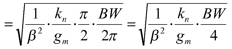
Inserting BW = =—— - , where GBW is the gain-bandwidth product and Ce = Cs + (Cint || Cp) , yields

Consequently, the output noise is independent of the
transconductance gm and therefore independent of the power consumption. The reason is that a smaller transconductance g increases noise, but at the same time reduces the gain- bandwidth product GBW, resulting in higher noise filtering. The calculation so far assumed that the GBW value is not relevant, i. e. the power consumption can be arbitrarily reduced at the cost of settling speed. However, typically there is a settling requirement related to feedback clock period T
r , T T T n
settling _ factor =—= =—= =— gm - fi (2)
BW
Solving equation (2) for Ceq and substituting the expression thus obtained in equation (1) yields
Vnoise out,rms = J— · settling _ factor
4 ' Tdk DAC · gm ■ β
The settling time is tied to the DAC clock period due to the pulsed nature of the feedback DAC. Using a non-pulsed continuous feedback current would alleviate the settling constraint. However, this does not provide the inherent analog-to-digital conversion present in the DAC based feedback .
Alternatively, a smoothing filter could be used after the DAC, but this can cause instability in a higher order feedback path. Furthermore, the feedback current does not
have a one to one correspondence to the DAC pulses, because it is not known how much of the current comes from the feedback pulses directly before and after output sampling. It is an object of the invention to provide power savings in current integration.
This object is achieved with the method of current
integration according to claim 1 and claim 8, respectively, and with the circuit for current integration according to claim 9 and claim 14, respectively. Variants and embodiments derive from the dependent claims.
The definitions as described above also apply to the
following description unless stated otherwise.
In one aspect of the invention, a method of current
integration is applied, which comprises transforming an input current into an output integrated voltage using a parallel connection of an operational transconductance amplifier (OTA) and an integration capacitor, reducing the output integrated voltage by repeatedly discharging the integration capacitor through a feedback loop via a digital-to-analog converter (DAC) generating feedback pulses, a feedback clock period defining time intervals between successive rising edges of the feedback pulses, and sampling during an extended feedback clock period after a lapse of a plurality of feedback clock periods. The extended feedback clock period may especially be twice as long as the feedback clock period.
In a variant of the method, the gain-bandwidth product (GBW) of the operational transconductance amplifier is reduced during sampling.
In a further variant of the method, a range check is
performed for the output integrated voltage before sampling. The range check is based on the number of feedback pulses occurring prior to sampling.
In further variants of the method, a switched capacitor digital-to-analog converter or a switched current source digital-to-analog converter is applied.
In a further variant of the method, further feedback pulses are generated between the feedback pulses generated by the digital-to-analog converter. For this purpose a further digital-to-analog converter is applied in the feedback loop.
In a further aspect of the invention, the method of current integration comprises transforming an input current into an output integrated voltage using a parallel connection of an operational transconductance amplifier and an integration capacitor, reducing the output integrated voltage by
repeatedly discharging the integration capacitor through a feedback loop via a digital-to-analog converter generating feedback pulses, applying an electric power for the
operational transconductance amplifier, and elevating the applied electric power only for sampling during a sampling time .
In a further aspect of the invention, a circuit for current integration is provided, which comprises a parallel
connection of an integration capacitor, an operational transconductance amplifier and a feedback loop, the
operational transconductance amplifier being configured to transform an input current into an output integrated voltage,
a digital-to-analog converter in the feedback loop, the digital-to-analog converter being configured to generate feedback pulses triggering discharges of the integration capacitor, a feedback clock period defining time intervals between successive rising edges of the feedback pulses, and a controller configured to provide an extended feedback clock period after a lapse of a plurality of feedback clock periods . In an embodiment of the circuit, the controller is configured to perform a range check for the output integrated voltage before sampling, the range check being based on a number of feedback pulses prior to sampling. In further embodiments of the circuit, the digital-to-analog converter is a switched capacitor digital-to-analog converter or a switched current source digital-to-analog converter.
A further embodiment of the circuit comprises a further digital-to-analog converter in the feedback loop, the
controller being configured to enable an alternative
operation of the digital-to-analog converter and the further digital-to-analog converter. In a further aspect of the invention, the circuit comprises a parallel connection of an integration capacitor, an
operational transconductance amplifier and a feedback loop, the operational transconductance amplifier being configured to transform an input current into an output integrated voltage, a digital-to-analog converter in the feedback loop, the digital-to-analog converter being configured to generate feedback pulses triggering discharges of the integration capacitor, a supply of electric power for the operational
transconductance amplifier, and a controller configured to elevate the applied electric power only during sampling.
The method can be implemented, for example, by one of the corresponding embodiments of the current integration circuit.
The following is a more detailed description of examples of the method and the circuit in conjunction with the appended figures .
Figure 1 shows timing diagrams for unmodulated operation,
sampling time modulation and power modulation.
Figure 2 shows timing diagrams for sampling time modulation.
Figure 3 shows circuit diagrams for GBW reduction of the OTA.
Figure 4 shows an embodiment of the circuit.
Figure 5 shows a timing diagram for the embodiment according to Figure 4.
Figure 6 shows a circuit diagram for a current integrator
with feedback and a corresponding timing diagram.
According to one aspect of the invention, doubling the Tcik DAC takes place during the last cycle, just before sampling, depending on the input current level. As the noise of the OTA is not integrated, only the instantaneous noise during the sampling instant is relevant. The OTA noise power during the rest of the integration time is irrelevant. For input levels below half range of the input current, the frequency of the feedback pulse is smaller than the clock frequency (in the
example of Figure lb, the frequency of the pulses shown as " out a" is half the frequency of the clock signal "elk") .
When the OTA is allowed to settle longer by increasing the feedback clock period Tcik DAC, a smaller transconductance gm is required and therefore less power for the same output noise. However, the feedback clock period Tcik DAC is tied to the frequency of feedback pulses needed to keep the output integrated voltage Vout ±nt in the required voltage range.
Hence, the speed of the OTA can be set high during the major integration time but lower for higher noise filtering during the last cycle right before the sampling instant, if the signal range during that cycle is below half range. The last condition is important, because the last DAC clock cycle has to be doubled, thus allowing only one feedback pulse to occur .
As a result, low noise performance is achieved for the lower signal range where high SNR (signal-to-noise ratio) is most important. For the larger input range, the noise of the DAC is dominant, making the higher OTA noise insignificant.
Increasing the DAC period for the last cycle by a factor N increases the available time for settling by N, thus
resulting in a factor N power saving for the same output noise (assuming the power is proportional to gm which is the case for OTA input transistors close to weak inversion) .
A timing diagram for a conventional operation is depicted in Figure la, which shows the temporal variation of the relevant signals, quantities and parameters on a time line pointing towards the right. The signal indicated as "elk" is the clock signal providing the clock period Tcik as the minimum time
unit employed in the circuit. The signal indicated as
"sample" is high only during the sampling time, which in this example equals the clock period Tcik. The signal indicated as "clkDAC" is the clock signal provided for the feedback loop and is the same as the signal "elk" during conventional operation. Hence in Figure la the feedback clock period
Tcik DAc is the same as the clock period Ται¾. "Vout a" is the feedback voltage indicated in Figure 6a. "Ι±η" is the input current, which is assumed to be constant in the example of Figure la. "Vout int" is the output integrated voltage, which is indicated in the circuit diagram of Figure 6a. "GBW" is the gain-bandwidth product of the OTA, "gm" is the
transconductance of the OTA and "P" is the consumed power of the OTA.
A timing diagram for operation by sampling time modulation is depicted in Figure lb. Compared with the conventional
operation according to Figure la, the feedback clock period Tcik DAc that corresponds to the sampling time Tsampie is
increased. In the example shown in Figure lb, sampling is performed during an extended feedback clock period T*, which is N times as long (in the example of Figure lb especially twice as long) as the regular feedback clock period Ται¾ DAC- Moreover, the GBW is reduced during sampling. Thus the sampling time is increased, especially doubled.
In a prescribed time interval, which is highlighted in Figure lb, a range check is performed based on the number of
feedback pulses immediately prior to sampling. Important for the feasibility is the assumption that the time constant of the input current is significantly below the sampling time. This constraint does not result in loss of signal
information, because the total integration time is a multiple of the feedback clock period Tcik DAC .
In Figure 2 two different scenarios are exemplified. The worst case scenario in terms of the range of the output integrated voltage Vout ±ntr which is depicted in Figure 2a, occurs for half range input when the output integrated voltage Vout ±nt is just below the reference voltage Vref
(indicated in Figure 6a) upon entering the sample period, i. e. feedback is not triggered. This results in the maximal possible value of the output integrated voltage Vout ±nt at the moment when sampling is required, because the next feedback pulse is delayed by two clock periods Tcik. However, as shown in Figure 2a, by limiting the application of the extended feedback clock period T* to input signals below half range, the risk of exceeding the allowed output range can be
obviated .
For signals above half range, Tcik DAC is kept equal to Tcik to avoid out of range conditions, according to Figure 2b, corresponding to a conventional operation according to Figure la. As in this regime DAC noise is typically dominant, the power consumption can still be reduced to one half compared to the power consumption for conventional operation.
A timing diagram for an alternative operation by power modulation is depicted in Figure lc. In the method according to Figure lc, the feedback clock period Tcik DAC is kept constant, but the supply power P and the transconductance gm are increased during sampling in combination with a reduction of the GBW of the OTA. In this way the majority of clock cycles can run at reduced power. However, the increase in supply current in the last cycle can result in supply noise,
thus deteriorating accuracy. If a large number of parallel integrators with shifted sampling times is integrated on one chip, the supply current pulsing might smooth out on the main supply line.
The GBW of the OTA during sampling can either be reduced by implementing additional load capacitance, which may be achieved with the circuit according to Figure 3a, or by attenuating the output current of the OTA during sampling, which may be achieved with the circuit according to Figure 3b. The GBW can also be reduced by lowering the
transconductance gm, but this would not yield any benefit regarding noise. Figure 3a is a diagram of a circuit for adding a load
capacitor, which can be implemented in the OTA. The inputs and the output of the OTA are indicated by the corresponding voltages Vin ", Vin + and Vout OTA- Figure 3a also shows the connection of the integration capacitor Cint between the negative Input (Vin ") and the output (Vout OTA) of the OTA.
Figure 3b is a diagram of a circuit for reducing the output current, which can be implemented in the OTA. The inputs and the output of the OTA are indicated by the corresponding voltages Vin ", Vin + and Vout OTA- Figure 3b also shows the connection of the integration capacitor Cint between the negative Input (Vin ") and the output (Vout OTA) of the OTA.
Figure 4 is a circuit diagram for a device wherein the described method can be employed. The device may be a photocurrent readout circuit. The photodiode current is converted to a voltage by a current controlled oscillator.
The total number of feedback pulses ncounti + ncount2 during one full integration period Tint provides a coarse analog to digital conversion value, which is combined with a fine conversion result by digitization of the output voltage residue Vresidue of the current integrator. DAC feedback is realized by precharged capacitors that are periodically discharged into the virtual ground node. Two equivalent switched capacitor digital-to-analog converters SC DAC1, SC DAC2 are implemented. The first switched capacitor
digital-to-analog converter SC DAC1 is always active by default. The second switched capacitor digital-to-analog converter SC DAC2 is activated in case two consecutive DAC pulses are required. In this way, after triggering the first switched capacitor digital-to-analog converter SC DAC1, at least the time interval of one clock period is provided for precharging before the first switched capacitor digital-to- analog converter SC DAC1 is triggered again. According to this concept, the second switched capacitor digital-to-analog converter SC DAC2 is only activated for input currents above half range. Activation of the second switched capacitor digital-to-analog converter SC DAC2 triggers an
"out_of_range" flag that prevents activation of the double sampling time scheme for large input currents. Figure 5 is a timing diagram for the operation of a device comprising the circuit according to Figure 4. "Tint" is the integration period between two sampling events. "Vpuisei" and " pUise2" are the pulsed voltages provided by the controller as indicated in Figure 4. An out-of-range condition is present when the signal "out_of_range" is high. Figure 5 shows how the second switched capacitor digital-to-analog converter SC DAC2 is used after triggering the first switched capacitor digital-to-analog converter SC DAC1 in out-of-range
conditions, when immediately successive feedback pulses are required and there is no time for sufficient recovery of the first switched-capacitor digital-to-analog converter SC DAC1 after triggering. In an out-of-range condition, sampling is only performed for a time interval corresponding to the regular feedback clock period Tcik 0TA (which is indicated at position "A" in Figure 5) , whereas the sampling time is increased when no such condition is met (which is indicated at position "B" in Figure 5) .
This invention enables to reduce the power consumed in an integration stage for output residual sampling by a factor N, in particular by a factor of two.
List of reference numerals
Cint integration capacitor
elk clock signal
clkDAC feedback clock signal
DAC digital-to-analog converter
GBW gain-bandwidth product
gm transconductance
Iin input current
OTA operational transconductance amplifier
P power
sample sampling signal
SC DAC1 first switched capacitor digital-to-analog converter
SC DAC2 second switched capacitor digital-to-analog converter Tcik clock period
Tcik DAc feedback clock period
T* extended feedback clock period
Tsample sampling time
Vin" negative input of the OTA
Vin+ positive input of the OTA
Vout a feedback voltage
Vout im output integrated voltage
out OTA output of the OTA
Vpuigei first pulsed voltage
VpUiSE2 second pulsed voltage
Vref reference voltage
Vresidue output voltage residue
Claims
1. A method of current integration, comprising:
transforming an input current (Ι±η) into an output integrated voltage (Vout ±nt) using a parallel connection of an
operational transconductance amplifier (OTA) and an
integration capacitor (Cint) ,
reducing the output integrated voltage (Vout ±nt) by repeatedly discharging the integration capacitor (Cint) through a
feedback loop via a digital-to-analog converter (DAC,
SC DAC1) generating feedback pulses, a feedback clock period (Tcik DAC) defining time intervals between successive rising edges of the feedback pulses, and
sampling during an extended feedback clock period (T*) after a lapse of a plurality of feedback clock periods (Tcik DAC) .
2. The method of claim 1, wherein
the extended feedback clock period (T*) is N times as long as the feedback clock period (Tcik DAC) .
3. The method of claim 1 or 2, further comprising:
reducing a gain-bandwidth product (GBW) of the operational transconductance amplifier (OTA) during sampling.
4. The method of one of claims 1 to 3, further comprising: performing a range check for the output integrated voltage (Vout int) before sampling, the range check being based on a number of feedback pulses prior to sampling.
5. The method of one of claims 1 to 4, wherein
the digital-to-analog converter (DAC, SC DAC1) is a switched capacitor digital-to-analog converter.
6. The method of one of claims 1 to 4, wherein
the digital-to-analog converter (DAC) is a switched current source digital-to-analog converter.
7. The method of one of claims 1 to 6, further comprising: generating further feedback pulses between the feedback pulses generated by the digital-to-analog converter (SC DAC1) by applying a further digital-to-analog converter (SC DAC2) in the feedback loop.
8. A method of current integration, comprising:
transforming an input current (Ι±η) into an output integrated voltage (Vout ±nt) using a parallel connection of an
operational transconductance amplifier (OTA) and an
integration capacitor (Cint) r
reducing the output integrated voltage (Vout ±nt) by repeatedly discharging the integration capacitor (Cint) through a feedback loop via a digital-to-analog converter (DAC,
SC DAC1) generating feedback pulses,
applying an electric power (P) for the operational
transconductance amplifier (OTA) , and
elevating the applied electric power (P) only for sampling during a sampling time (Tsampie) .
9. A circuit for current integration, comprising:
a parallel connection of an integration capacitor (Cint) t an operational transconductance amplifier (OTA) and a feedback loop, the operational transconductance amplifier (OTA) being configured to transform an input current (Iin) into an output integrated voltage (Vout int) ,
a digital-to-analog converter (DAC, SC DAC1) in the feedback loop, the digital-to-analog converter (DAC, SC DAC1) being configured to generate feedback pulses triggering discharges
of the integration capacitor (Cint) , a feedback clock period (Tcik DAC) defining time intervals between successive rising edges of the feedback pulses, and
a controller configured to provide an extended feedback clock period (T*) after a lapse of a plurality of feedback clock periods (Tcik_DAC) .
10. The circuit of claim 9, wherein:
the controller is configured to perform a range check for the output integrated voltage (Vout ±nt) before sampling, the range check being based on a number of feedback pulses prior to sampling .
11. The circuit of claim 9 or 10, wherein
the digital-to-analog converter (DAC, SC DAC1) is a switched capacitor digital-to-analog converter.
12. The circuit of claim 9 or 10, wherein
the digital-to-analog converter (DAC) is a switched current source digital-to-analog converter.
13. The circuit of one of claims 9 to 12, further comprising: a further digital-to-analog converter (SC DAC2) in the feedback loop, the controller being configured to enable an alternative operation of the digital-to-analog converter (SC DAC1) and the further digital-to-analog converter
(SC DAC2 ) .
14. A circuit for current integration, comprising:
a parallel connection of an integration capacitor (Cint) an operational transconductance amplifier (OTA) and a feedback loop, the operational transconductance amplifier (OTA) being
configured to transform an input current (Ι±η) into an output integrated voltage (Vout ±nt) ,
a digital-to-analog converter (DAC, SC DAC1) in the feedback loop, the digital-to-analog converter (DAC, SC DAC1) being configured to generate feedback pulses triggering discharges of the integration capacitor (Cint) ,
a supply of electric power (P) for the operational
transconductance amplifier (OTA) , and
a controller configured to elevate the applied electric power (P) only during sampling.
Priority Applications (2)
| Application Number | Priority Date | Filing Date | Title |
|---|---|---|---|
| US16/629,139 US10951222B2 (en) | 2017-07-13 | 2018-07-04 | Method and circuit for current integration |
| CN201880045533.8A CN110870206B (en) | 2017-07-13 | 2018-07-04 | Current integration method and circuit |
Applications Claiming Priority (2)
| Application Number | Priority Date | Filing Date | Title |
|---|---|---|---|
| EP17181215.9A EP3429083B1 (en) | 2017-07-13 | 2017-07-13 | Method and circuit for current integration |
| EP17181215.9 | 2017-07-13 |
Publications (1)
| Publication Number | Publication Date |
|---|---|
| WO2019011749A1 true WO2019011749A1 (en) | 2019-01-17 |
Family
ID=59337562
Family Applications (1)
| Application Number | Title | Priority Date | Filing Date |
|---|---|---|---|
| PCT/EP2018/068103 Ceased WO2019011749A1 (en) | 2017-07-13 | 2018-07-04 | Method and circuit for current integration |
Country Status (5)
| Country | Link |
|---|---|
| US (1) | US10951222B2 (en) |
| EP (1) | EP3429083B1 (en) |
| CN (1) | CN110870206B (en) |
| TW (1) | TWI775881B (en) |
| WO (1) | WO2019011749A1 (en) |
Cited By (1)
| Publication number | Priority date | Publication date | Assignee | Title |
|---|---|---|---|---|
| EP3839833A1 (en) * | 2019-12-16 | 2021-06-23 | ams International AG | Neural amplifier, neural network and sensor device |
Citations (3)
| Publication number | Priority date | Publication date | Assignee | Title |
|---|---|---|---|---|
| US6366231B1 (en) * | 2000-04-10 | 2002-04-02 | General Electric Company | Integrate and fold analog-to-digital converter with saturation prevention |
| US20020175844A1 (en) * | 2001-05-25 | 2002-11-28 | Elmar Bach | High-speed sample-and-hold circuit with gain |
| EP1594230A1 (en) * | 2004-05-05 | 2005-11-09 | STMicroelectronics S.r.l. | Switched capacitance circuit |
Family Cites Families (17)
| Publication number | Priority date | Publication date | Assignee | Title |
|---|---|---|---|---|
| US4939516B1 (en) * | 1988-06-13 | 1993-10-26 | Crystal Semiconductor Corporation | Chopper stabilized delta-sigma analog-to-digital converter |
| US6744394B2 (en) * | 2002-05-10 | 2004-06-01 | 02Micro International Limited | High precision analog to digital converter |
| US6778009B1 (en) * | 2002-10-31 | 2004-08-17 | National Semiconductor Corporation | High gain and wide bandwidth switched capacitor amplifier having a dynamically loaded amplifier output |
| US6750796B1 (en) * | 2003-03-27 | 2004-06-15 | National Semiconductor Corporation | Low noise correlated double sampling modulation system |
| US6869216B1 (en) * | 2003-03-27 | 2005-03-22 | National Semiconductor Corporation | Digitizing temperature measurement system |
| DE102004022572B4 (en) * | 2004-05-07 | 2012-02-16 | Infineon Technologies Ag | integrator circuit |
| US8030999B2 (en) * | 2004-09-20 | 2011-10-04 | The Trustees Of Columbia University In The City Of New York | Low voltage operational transconductance amplifier circuits |
| DE102005042710B4 (en) * | 2005-09-09 | 2007-04-26 | Infineon Technologies Ag | Device and method for the spectral shaping of a reference clock signal |
| WO2010119456A2 (en) * | 2009-04-03 | 2010-10-21 | Secretary, Department Of Information Technology (Dit) | Method and apparatus for low power continuous time delta sigma modulation |
| US9459833B2 (en) * | 2012-09-28 | 2016-10-04 | Maxim Integrated Products, Inc. | System and method with specific ordered execution over physical elements |
| US8614587B1 (en) * | 2013-03-12 | 2013-12-24 | Cypress Semiconductor Corp. | Capacitance sensing circuits and methods |
| US9218883B2 (en) * | 2013-03-15 | 2015-12-22 | West Virginia University | Continuous-time floating gate memory cell programming |
| US9197241B2 (en) * | 2013-12-20 | 2015-11-24 | Nokia Technologies Oy | Output power control for RF digital-to-analog converter |
| CN106027060B (en) * | 2016-05-20 | 2019-02-26 | 复旦大学 | An Input Feedforward Delta-Sigma Modulator |
| US10027338B2 (en) * | 2016-06-10 | 2018-07-17 | Analog Devices Global | Buffer, and digital to analog converter in combination with a buffer |
| US10243578B2 (en) * | 2017-02-23 | 2019-03-26 | Qualcomm Incorporated | Continuous-time delta-sigma ADC with scalable sampling rates and excess loop delay compensation |
| US10103744B1 (en) * | 2017-04-12 | 2018-10-16 | Analog Devices Global | Power scaling a continuous-time delta sigma modulator |
-
2017
- 2017-07-13 EP EP17181215.9A patent/EP3429083B1/en active Active
-
2018
- 2018-06-25 TW TW107121705A patent/TWI775881B/en active
- 2018-07-04 US US16/629,139 patent/US10951222B2/en active Active
- 2018-07-04 WO PCT/EP2018/068103 patent/WO2019011749A1/en not_active Ceased
- 2018-07-04 CN CN201880045533.8A patent/CN110870206B/en active Active
Patent Citations (3)
| Publication number | Priority date | Publication date | Assignee | Title |
|---|---|---|---|---|
| US6366231B1 (en) * | 2000-04-10 | 2002-04-02 | General Electric Company | Integrate and fold analog-to-digital converter with saturation prevention |
| US20020175844A1 (en) * | 2001-05-25 | 2002-11-28 | Elmar Bach | High-speed sample-and-hold circuit with gain |
| EP1594230A1 (en) * | 2004-05-05 | 2005-11-09 | STMicroelectronics S.r.l. | Switched capacitance circuit |
Cited By (2)
| Publication number | Priority date | Publication date | Assignee | Title |
|---|---|---|---|---|
| EP3839833A1 (en) * | 2019-12-16 | 2021-06-23 | ams International AG | Neural amplifier, neural network and sensor device |
| WO2021121820A1 (en) * | 2019-12-16 | 2021-06-24 | Ams International Ag | Neural amplifier, neural network and sensor device |
Also Published As
| Publication number | Publication date |
|---|---|
| TWI775881B (en) | 2022-09-01 |
| CN110870206A (en) | 2020-03-06 |
| US20200295774A1 (en) | 2020-09-17 |
| CN110870206B (en) | 2023-07-04 |
| EP3429083A1 (en) | 2019-01-16 |
| TW201918035A (en) | 2019-05-01 |
| US10951222B2 (en) | 2021-03-16 |
| EP3429083B1 (en) | 2020-09-02 |
Similar Documents
| Publication | Publication Date | Title |
|---|---|---|
| US7652603B2 (en) | ΔΣ-type AD converter, class-D amplifier, and DC-DC converter | |
| US9136867B2 (en) | ΔΣ-modulator and ΔΣ-A/D converter | |
| JP4774159B2 (en) | Integration and folding circuit for analog-digital conversion | |
| US9806733B1 (en) | Hybrid analog-to-digital converter | |
| US20220163572A1 (en) | Amplification interface, and corresponding measurement system and method for calibrating an amplification interface | |
| US20060187097A1 (en) | Sigma delta converter with flying capacitor input | |
| US6417725B1 (en) | High speed reference buffer | |
| KR20150108119A (en) | Ramp Signal Generator, and CMOS Image Sensor Using That | |
| US10951222B2 (en) | Method and circuit for current integration | |
| US6400214B1 (en) | Switched capacitor filter for reference voltages in analog to digital converter | |
| Wittmann et al. | A 12V 10MHz buck converter with dead time control based on a 125 ps differential delay chain | |
| US11515861B2 (en) | Electronic apparatus comprising a switching-type output stage, corresponding circuit arrangement and method | |
| US11349439B2 (en) | Method for amplifier load current cancellation in a current integrator and current integrator with amplifier load current cancellation | |
| US7423566B2 (en) | Sigma-delta modulator using a passive filter | |
| JP2015023544A (en) | Signal conversion device | |
| Smedley | Digital-PWM audio power amplifiers with noise and ripple shaping | |
| Miao et al. | ∑ Δ ADC based current mode power supply controller with digital voltage loop | |
| JP2026002271A (en) | Analog-to-digital conversion device and optical sensor | |
| HK1179059B (en) | A method for signal measuring | |
| HK1179059A1 (en) | A method for signal measuring |
Legal Events
| Date | Code | Title | Description |
|---|---|---|---|
| 121 | Ep: the epo has been informed by wipo that ep was designated in this application |
Ref document number: 18736904 Country of ref document: EP Kind code of ref document: A1 |
|
| NENP | Non-entry into the national phase |
Ref country code: DE |
|
| 122 | Ep: pct application non-entry in european phase |
Ref document number: 18736904 Country of ref document: EP Kind code of ref document: A1 |