WO2018181235A1 - 圧力センサ内蔵ディスプレイ - Google Patents
圧力センサ内蔵ディスプレイ Download PDFInfo
- Publication number
- WO2018181235A1 WO2018181235A1 PCT/JP2018/012276 JP2018012276W WO2018181235A1 WO 2018181235 A1 WO2018181235 A1 WO 2018181235A1 JP 2018012276 W JP2018012276 W JP 2018012276W WO 2018181235 A1 WO2018181235 A1 WO 2018181235A1
- Authority
- WO
- WIPO (PCT)
- Prior art keywords
- pressure sensor
- display
- touch
- pressure
- built
- Prior art date
- Legal status (The legal status is an assumption and is not a legal conclusion. Google has not performed a legal analysis and makes no representation as to the accuracy of the status listed.)
- Ceased
Links
Images




Classifications
-
- G—PHYSICS
- G06—COMPUTING OR CALCULATING; COUNTING
- G06F—ELECTRIC DIGITAL DATA PROCESSING
- G06F3/00—Input arrangements for transferring data to be processed into a form capable of being handled by the computer; Output arrangements for transferring data from processing unit to output unit, e.g. interface arrangements
- G06F3/01—Input arrangements or combined input and output arrangements for interaction between user and computer
- G06F3/03—Arrangements for converting the position or the displacement of a member into a coded form
- G06F3/041—Digitisers, e.g. for touch screens or touch pads, characterised by the transducing means
- G06F3/044—Digitisers, e.g. for touch screens or touch pads, characterised by the transducing means by capacitive means
- G06F3/0443—Digitisers, e.g. for touch screens or touch pads, characterised by the transducing means by capacitive means using a single layer of sensing electrodes
-
- G—PHYSICS
- G02—OPTICS
- G02F—OPTICAL DEVICES OR ARRANGEMENTS FOR THE CONTROL OF LIGHT BY MODIFICATION OF THE OPTICAL PROPERTIES OF THE MEDIA OF THE ELEMENTS INVOLVED THEREIN; NON-LINEAR OPTICS; FREQUENCY-CHANGING OF LIGHT; OPTICAL LOGIC ELEMENTS; OPTICAL ANALOGUE/DIGITAL CONVERTERS
- G02F1/00—Devices or arrangements for the control of the intensity, colour, phase, polarisation or direction of light arriving from an independent light source, e.g. switching, gating or modulating; Non-linear optics
- G02F1/01—Devices or arrangements for the control of the intensity, colour, phase, polarisation or direction of light arriving from an independent light source, e.g. switching, gating or modulating; Non-linear optics for the control of the intensity, phase, polarisation or colour
- G02F1/13—Devices or arrangements for the control of the intensity, colour, phase, polarisation or direction of light arriving from an independent light source, e.g. switching, gating or modulating; Non-linear optics for the control of the intensity, phase, polarisation or colour based on liquid crystals, e.g. single liquid crystal display cells
- G02F1/133—Constructional arrangements; Operation of liquid crystal cells; Circuit arrangements
- G02F1/1333—Constructional arrangements; Manufacturing methods
- G02F1/13338—Input devices, e.g. touch panels
-
- G—PHYSICS
- G06—COMPUTING OR CALCULATING; COUNTING
- G06F—ELECTRIC DIGITAL DATA PROCESSING
- G06F3/00—Input arrangements for transferring data to be processed into a form capable of being handled by the computer; Output arrangements for transferring data from processing unit to output unit, e.g. interface arrangements
- G06F3/01—Input arrangements or combined input and output arrangements for interaction between user and computer
- G06F3/03—Arrangements for converting the position or the displacement of a member into a coded form
- G06F3/041—Digitisers, e.g. for touch screens or touch pads, characterised by the transducing means
- G06F3/0412—Digitisers structurally integrated in a display
-
- G—PHYSICS
- G06—COMPUTING OR CALCULATING; COUNTING
- G06F—ELECTRIC DIGITAL DATA PROCESSING
- G06F3/00—Input arrangements for transferring data to be processed into a form capable of being handled by the computer; Output arrangements for transferring data from processing unit to output unit, e.g. interface arrangements
- G06F3/01—Input arrangements or combined input and output arrangements for interaction between user and computer
- G06F3/03—Arrangements for converting the position or the displacement of a member into a coded form
- G06F3/041—Digitisers, e.g. for touch screens or touch pads, characterised by the transducing means
- G06F3/0416—Control or interface arrangements specially adapted for digitisers
- G06F3/04166—Details of scanning methods, e.g. sampling time, grouping of sub areas or time sharing with display driving
-
- G—PHYSICS
- G06—COMPUTING OR CALCULATING; COUNTING
- G06F—ELECTRIC DIGITAL DATA PROCESSING
- G06F3/00—Input arrangements for transferring data to be processed into a form capable of being handled by the computer; Output arrangements for transferring data from processing unit to output unit, e.g. interface arrangements
- G06F3/01—Input arrangements or combined input and output arrangements for interaction between user and computer
- G06F3/03—Arrangements for converting the position or the displacement of a member into a coded form
- G06F3/041—Digitisers, e.g. for touch screens or touch pads, characterised by the transducing means
- G06F3/044—Digitisers, e.g. for touch screens or touch pads, characterised by the transducing means by capacitive means
- G06F3/0446—Digitisers, e.g. for touch screens or touch pads, characterised by the transducing means by capacitive means using a grid-like structure of electrodes in at least two directions, e.g. using row and column electrodes
-
- G—PHYSICS
- G06—COMPUTING OR CALCULATING; COUNTING
- G06F—ELECTRIC DIGITAL DATA PROCESSING
- G06F3/00—Input arrangements for transferring data to be processed into a form capable of being handled by the computer; Output arrangements for transferring data from processing unit to output unit, e.g. interface arrangements
- G06F3/01—Input arrangements or combined input and output arrangements for interaction between user and computer
- G06F3/03—Arrangements for converting the position or the displacement of a member into a coded form
- G06F3/041—Digitisers, e.g. for touch screens or touch pads, characterised by the transducing means
- G06F3/044—Digitisers, e.g. for touch screens or touch pads, characterised by the transducing means by capacitive means
- G06F3/0447—Position sensing using the local deformation of sensor cells
-
- G—PHYSICS
- G02—OPTICS
- G02F—OPTICAL DEVICES OR ARRANGEMENTS FOR THE CONTROL OF LIGHT BY MODIFICATION OF THE OPTICAL PROPERTIES OF THE MEDIA OF THE ELEMENTS INVOLVED THEREIN; NON-LINEAR OPTICS; FREQUENCY-CHANGING OF LIGHT; OPTICAL LOGIC ELEMENTS; OPTICAL ANALOGUE/DIGITAL CONVERTERS
- G02F1/00—Devices or arrangements for the control of the intensity, colour, phase, polarisation or direction of light arriving from an independent light source, e.g. switching, gating or modulating; Non-linear optics
- G02F1/01—Devices or arrangements for the control of the intensity, colour, phase, polarisation or direction of light arriving from an independent light source, e.g. switching, gating or modulating; Non-linear optics for the control of the intensity, phase, polarisation or colour
- G02F1/13—Devices or arrangements for the control of the intensity, colour, phase, polarisation or direction of light arriving from an independent light source, e.g. switching, gating or modulating; Non-linear optics for the control of the intensity, phase, polarisation or colour based on liquid crystals, e.g. single liquid crystal display cells
- G02F1/133—Constructional arrangements; Operation of liquid crystal cells; Circuit arrangements
- G02F1/1333—Constructional arrangements; Manufacturing methods
- G02F1/1343—Electrodes
- G02F1/134309—Electrodes characterised by their geometrical arrangement
-
- G—PHYSICS
- G06—COMPUTING OR CALCULATING; COUNTING
- G06F—ELECTRIC DIGITAL DATA PROCESSING
- G06F2203/00—Indexing scheme relating to G06F3/00 - G06F3/048
- G06F2203/041—Indexing scheme relating to G06F3/041 - G06F3/045
- G06F2203/04105—Pressure sensors for measuring the pressure or force exerted on the touch surface without providing the touch position
Definitions
- the present invention relates to a pressure sensor built-in display including a capacitive touch sensor that detects a touch on a counter substrate facing a circuit board, and a pressure sensor that detects a pressure applied to the counter substrate.
- An input device for an electronic device incorporating a pressure sensor is known as a prior art (Patent Document 1).
- the input device includes a first substrate having an input surface.
- the first substrate is provided with a plurality of sense electrodes for detecting proximity of an input target.
- a pair of pressure detection electrodes is provided on the back side of the first substrate.
- the input device includes a second substrate.
- the second substrate has a leaf spring including a peripheral region surrounding the internal region.
- the input device includes a space layer. The space layer is configured to physically couple the inner region of the second substrate to the first substrate.
- the pressure sensor can distinguish between the press touch and the feather touch, it is possible to reduce the mistaken operation of the conventional touch panel and provide a more intuitive and stress-free user interface. For this reason, attention has recently been paid to the incorporation of a pressure sensor in a display device.
- the display device incorporates the touch sensor and the pressure sensor separately, the display device is thick. Circuits and controllers related to the touch sensor and the pressure sensor are also provided separately for the touch sensor and the pressure sensor. Therefore, the manufacturing and assembly processes become complicated and the design rules become more strict. Costs also increased.
- An object of one embodiment of the present invention is to realize a low-cost and compact display with a built-in pressure sensor.
- a display with a built-in pressure sensor includes a circuit board, a counter substrate disposed to face the circuit board, and the circuit board and the counter substrate.
- a display layer formed on the counter substrate a capacitance type touch sensor that detects a touch on the counter substrate, and a pressure sensor that detects a pressure applied to the counter substrate.
- a plurality of touch pad electrodes disposed on the display layer side, and the pressure sensor includes a plurality of pressure pad electrodes disposed on the display layer side of the circuit board and the display layer of the counter substrate. And a plurality of drive electrodes arranged on the side.
- FIG. 1 is sectional drawing which shows the principal part structure of the display with a built-in pressure sensor which concerns on Embodiment 1
- (b) is sectional drawing which shows schematic structure of the said display with a built-in pressure sensor.
- (A) is a figure for demonstrating operation
- (b) is a model of the structure of the pressure sensor provided with the said display with a built-in pressure sensor.
- FIG. It is a schematic diagram which shows the structure of the circuit board and counter substrate which were provided in the said display with a built-in pressure sensor.
- (A) is a timing chart which shows operation
- (b) is a liquid crystal display part, a touch sensor, and a pressure sensor in a vertical blank period. It is a timing chart which shows the operation
- (A) is a schematic diagram for demonstrating operation
- (b) is a schematic diagram for demonstrating operation
- (A) is a top view which shows the structure of the circuit board provided in the display with a built-in pressure sensor which concerns on Embodiment 2
- (b) is a bottom view which shows the structure of the opposing board
- (A) is a top view which shows the structure of the circuit board provided in the display with a built-in pressure sensor which concerns on Embodiment 3
- (b) is a bottom view which shows the structure of the counter substrate provided in the said display with a built-in pressure sensor. is there.
- FIG. 1A is a cross-sectional view showing a main configuration of the pressure sensor built-in display 1 according to the first embodiment, and FIG.
- the pressure sensor built-in display 1 includes a circuit board 2, a counter substrate 3 disposed to face the circuit board 2, and a liquid crystal layer 4 (display layer) formed between the circuit board 2 and the counter substrate 3.
- a cover glass 22 is formed on the opposite side of the counter substrate 3 from the liquid crystal layer 4.
- the pressure sensor built-in display 1 is provided with a capacitive touch sensor 5 for detecting a touch on the counter substrate 3 and a pressure sensor 11 for detecting a pressure applied to the counter substrate 3.
- the touch sensor 5 has a plurality of touch pad electrodes 7 disposed on the liquid crystal layer 4 side of the circuit board 2.
- the pressure sensor 11 includes a plurality of pressure pad electrodes 12 (common electrodes) disposed on the liquid crystal layer 4 side of the circuit board 2 and a plurality of drive electrodes 13 disposed on the liquid crystal layer 4 side of the counter substrate 3. Have.
- FIG. 2A is a diagram for explaining the operation of the touch pad electrode 7 of the self-capacitance type touch sensor 5 provided in the pressure sensor built-in display 1, and FIG. 3 is a cross-sectional view schematically showing the configuration of the pressure sensor 11.
- the touch pad electrode 7 is a self-capacitance type electrode provided so as to detect a capacitance or capacitance change between the finger 16 as a detection target.
- the pressure sensor 11 has a capacitance change between the pressure pad electrode 12 and the drive electrode 13 based on a change in the cell gap of the liquid crystal layer 4 between the circuit substrate 2 and the counter substrate 3. Is detected.
- FIG. 3 is a schematic diagram showing the configuration of the circuit board 2 and the counter substrate 3 provided in the pressure sensor built-in display 1.
- a plurality of touch pad electrodes 7 and a plurality of pressure pad electrodes 12 are arranged in a matrix on the circuit board 2.
- a plurality of pressure pad electrodes 12 are arranged in odd rows, and a plurality of touch pad electrodes 7 are arranged in even rows.
- a plurality of touch pad electrodes 7 may be arranged in odd rows, and a plurality of pressure pad electrodes 12 may be arranged in even rows.
- the pressure pad electrode 12 is shared with a common electrode for forming an electric field that controls the orientation of liquid crystal molecules contained in the liquid crystal layer 4.
- the touch pad electrode 7 is also used as a common electrode.
- the touch sensor 5 has a plurality of sense lines 6 respectively extending in the column direction (Y-axis direction) corresponding to each of the touch pad electrodes 7 arranged in each column.
- a plurality of common electrodes for forming an electric field for controlling the alignment of liquid crystal molecules contained in the liquid crystal layer 4 are arranged in a matrix as an electrode array. Then, a group of the electrode array detects a change in capacitance due to touch as a self-capacitance type touch pad electrode 7. Further, the remaining group of the electrode array detects the capacitance change due to the pressure together with the drive electrode 13 as the mutual capacitance type pressure pad electrode 12.
- a plurality of drive electrodes 13 are arranged to face the pressure pad electrode 12.
- the counter substrate 3 has a black matrix 15 formed in a lattice shape so as to partition three color filter layers arranged periodically.
- a plurality of drive electrodes 13 are formed on the black matrix 15.
- the three color filter layers constitute a color filter.
- the drive electrode 13 as a transmission electrode (Tx) for pressure detection is patterned on the black matrix 15 of the counter substrate 3.
- the transmission electrode is patterned so as to overlap with the pressure pad electrode 12 as the reception electrode (Rx) for pressure detection disposed on the circuit board 2.
- the circuit board 2 includes a self-capacitance controller 17 coupled to each of a plurality of touch pad electrodes 7 via a sense line 6, a pressure pad electrode 12 arranged in each column, and a single pressure sense line 20. And a mutual capacitance controller 18 coupled to each other.
- the self-capacitance controller 17 and the mutual capacitance controller 18 are connected to the timing control circuit 19.
- the timing control circuit 19 controls the timing and synchronization of liquid crystal display, touch detection, and pressure detection.
- the self-capacitance controller 17 is integrated in the display driver.
- the counter substrate 3 is provided with a mutual capacitance controller 21 connected to a plurality of drive electrodes 13.
- the mutual capacitance controller 21 is connected to the mutual capacitance controller 18 of the circuit board 2.
- FIG. 4A is a timing chart showing the operation of the liquid crystal display unit, the touch sensor 5 and the pressure sensor 11 provided in the pressure sensor built-in display 1, and FIG. 4B is the liquid crystal display unit and the touch sensor in the vertical blank period.
- 5 is a timing chart showing the operation of the pressure sensor 11 and the pressure sensor 11.
- the touch sensor 5 and the pressure sensor 11 operate based on the vertical synchronization of the display by the liquid crystal layer 4.
- the liquid crystal layer 4 (LCD) operates in the display writing period t1, and stops in the vertical blank period t2 following the display writing period t1.
- the sum of the display writing period t1 and the vertical blanking period t2 is 16.67 (ms, milliseconds).
- the scanning by the touch sensor 5 and the scanning by the pressure sensor 11 are executed in the display refresh period (vertical blank period t2) by the liquid crystal layer 4.
- the touch sensor 5 Since the touch sensor 5 is a self-capacitance type, the individual touch pad electrodes 7 are charged and discharged sequentially.
- the drive electrode 13 as the transmission electrode (Tx) of the pressure sensor 11 is electrically floating during the period when the touch pad electrode 7 of the self-capacitance type touch sensor 5 is charged in order to avoid an adverse effect on touch detection. State (floating state).
- FIG. 5 is a timing chart for explaining the synchronization of the operations of the touch sensor 5 and the pressure sensor 11.
- the pressure sensor enable signal (Force TX enable) rises from the low state (VL) to the high state (VH) at time T1
- the transmission signal applied to the drive electrode 13 as the transmission electrode (Tx) of the pressure sensor 11 also rises from the low state (VL) to the high state (VH).
- the read signal (Force SH) read from the pressure pad electrode 12 as the receiving electrode of the pressure sensor 11 rises from the low state (VL) to the high state (VH) at time T2.
- the read signal (Force SH) falls from the high state (VH) to the low state (VL) at time T3.
- the pressure sensor enable signal (Force TX enable) and the transmission signal (Force Tx) fall from the high state (VH) to the low state (VL).
- the transmission signal (Touch Tx) applied to the touch pad electrode 7 of the touch sensor 5 rises from the low state (VL) to the high state (VH) at time T5.
- the transmission signal (Touch Tx) falls from the high state (VH) to the low state (VL) at time T6
- the readout signal (Touch SH) read from the touch pad electrode 7 of the touch sensor 5 is low ( It rises from VL to high state (VH).
- the read signal (Touch SH) falls from the high state (VH) to the low state (VL) at time T7. Thereafter, the same operation is repeated.
- the transmission signal (Force ⁇ ⁇ Tx) applied to the drive electrode 13 as the transmission electrode (Tx) of the pressure sensor 11 is transmitted to the touch pad electrode 7 of the touch sensor 5 (Touch Tx).
- FIG. 6 is a timing chart for explaining another synchronization of the operation of the touch sensor 5 and the pressure sensor 11. The same components as those described above with reference to FIG. Detailed description of these components will not be repeated.
- the transmission signal (Touch Tx) applied to the touch pad electrode 7 of the touch sensor 5 rises from the low state (VL) to the high state (VH) at time T5
- the pressure sensor enable signal (Force TX enable) is also in the low state. It rises from (VL) to high state (VH).
- the transmission signal (Touch Tx) falls from the high state (VH) to the low state (VL) at time T6
- the pressure sensor enable signal (Force TX enable) also changes from the high state (VH) to the low state (VL). To fall.
- the transmission signal (Touch Tx) is driven by a pressure sensor enable signal (Force TX enable) similar to a touch sensing signal for reducing the parasitic capacitance on the electrodes of the touch sensor 5.
- FIG. 7A is a schematic diagram for explaining the operation of the pressure sensor 11
- FIG. 7B is a schematic diagram for explaining the operation of the touch sensor 5.
- the self-capacitance method requires a charging period and a discharging period, but the mutual capacitance method does not require a sensing period to be divided into a charging period and a discharging period.
- the pressure can be detected during a reading period from the touch pad electrode 7 of the touch sensor 5.
- the period for applying the transmission signal (Touch Tx) to the touch pad electrode 7 is reduced, and the touch pad electrode 7 and the period for reading the readout signal (Force SH) from the pressure pad electrode 12 can be extended.
- all pressure pad electrodes 12 on the circuit board 2 are connected to the mutual capacitance controller 18 as shown in FIG. And the signal from the pressure pad electrode 12 as a receiving electrode of the pressure sensor 11 is measured, and the pressure on a touch panel is determined.
- the drive electrode 13 of the pressure sensor 11 is in an electrically floating state (floating state).
- the pressure pad electrode 12 of the pressure sensor 11 is coupled to a signal similar to that of the touch pad electrode 7 to reduce the load capacitance on the touch pad electrode 7 and improve performance.
- FIG. 8A is a top view showing the configuration of the circuit board 2 provided in the pressure sensor built-in display according to the second embodiment, and FIG. 8B shows the configuration of the counter substrate 3 provided in the pressure sensor built-in display. It is a bottom view shown.
- the circuit board 2 includes a plurality of sense lines 6A extending in the Y direction (column direction) corresponding to the touch pad electrodes 7 and the pressure pad electrodes 12 arranged in each column, and the sense lines 6A and the touch pad electrodes. 7 and a plurality of switch elements 8 (first switch elements) formed between the sense line 6A and each pressure pad electrode 12, respectively.
- the circuit board 2 has a plurality of pressure pad electrodes 12 arranged in each row, and a plurality of multiplexers 25 connected to the plurality of touch pad electrodes 7 arranged in each row via drive lines 24, respectively.
- Each multiplexer 25 is connected to a scanning circuit 26.
- a selection line 23 extending in the X direction is connected to the scanning circuit 26 in order to control the plurality of switch elements 8.
- a transmission signal (Touch Tx) is applied to the drive electrode 13
- the switch element 8 of the pressure pad electrode 12 is turned on by the scanning circuit 26 via the selection line 23, and the switch element 8 and the switch element 8 from the pressure pad electrode 12 are turned on.
- a read signal (Force SH) is read through the sense line 6A.
- a transmission signal (TouchxTx) is applied to the touch pad electrode 7 by the scanning circuit 26 via the drive line 24 and the multiplexer 25.
- the switch element 8 of the touch pad electrode 7 is turned on by the scanning circuit 26 through the selection line 23, and a read signal (Touch SH) is read from the touch pad electrode 7 through the switch element 8 and the sense line 6A.
- FIG. 9A is a top view showing the configuration of the circuit board 2 provided in the pressure sensor built-in display according to Embodiment 3, and FIG. 9B shows the configuration of the counter substrate 3 provided in the pressure sensor built-in display. It is a bottom view shown.
- the pressure pad electrode 12 has two switch elements 8 and 9 (first switch element and second switch element).
- the switch element 8 is connected to the sense line 6A extending in the Y direction, and is controlled by the scanning circuit 26C through the selection line 23 extending in the X direction.
- the switch element 9 is connected to a drive line 24C extending in the X direction and controlled by the scanning circuit 26C through a selection line 23C extending in the X direction.
- the display 1 with a built-in pressure sensor is formed between a circuit board 2, a counter board 3 disposed to face the circuit board 2, and the circuit board 2 and the counter board 3.
- the touch sensor 5 has a plurality of touch pad electrodes 7 arranged on the display layer (liquid crystal layer 4) side of the circuit board 2, and the pressure sensor 11 is connected to the display layer (liquid crystal layer 4) of the circuit board 2.
- the touch pad electrode of the touch sensor is arranged on the display layer side of the circuit board.
- the pressure pad electrode of the pressure sensor is disposed on the display layer side of the circuit board, and the drive electrode of the pressure sensor is disposed on the display layer side of the counter substrate. For this reason, a pressure sensor and a touch sensor are built in the display. As a result, a low-cost and compact pressure sensor built-in display can be realized.
- the pressure sensor built-in display 1 according to aspect 2 of the present invention is the above-described aspect 1, wherein the plurality of touch pad electrodes 7 and the plurality of pressure pad electrodes 12 are arranged in a matrix, and the plurality of touch pad electrodes are arranged. 7 may be arranged in odd rows, and the plurality of pressure pad electrodes 12 may be arranged in even rows.
- the touch pad electrode and the pressure pad electrode can be simultaneously formed by the same manufacturing process.
- the plurality of drive electrodes 13 may be arranged to face the pressure pad electrodes 12 in the even-numbered rows.
- a mutual capacitance type pressure sensor can be configured by the drive electrode and the pressure pad electrode.
- the display layer is the liquid crystal layer 4 and the pressure pad electrode 12 is included in the liquid crystal layer 4. You may share with the common electrode for forming the electric field which controls the orientation of a liquid crystal molecule.
- the pressure pad electrode is shared with the common electrode, the pressure sensor built-in display is further reduced in cost and compact.
- a pressure sensor built-in display 1 according to an aspect 5 of the present invention is the color filter in which the counter substrate 3 is configured by periodically arranging three color filter layers in any one of the above aspects 1 to 4. And a black matrix 15 formed in a lattice shape to partition the three color filter layers, and the plurality of drive electrodes 13 may be formed in the black matrix 15.
- the drive electrode of the pressure sensor is formed in a black matrix formed in a lattice shape to partition the three color filter layers, the display with a built-in pressure sensor becomes even more compact.
- the pressure sensor built-in display 1 according to the aspect 6 of the present invention is the pressure sensor built-in display 1 according to any one of the above aspects 2 to 5, in which the touch sensor 5 is arranged in the column direction corresponding to the touch pad electrodes 7 arranged in each column. It further includes a plurality of extending sense lines 6, 6A, and a plurality of first switch elements (switch elements 8) formed between the sense lines 6, 6A and the touch pad electrodes 7, respectively. Good.
- the readout signal can be read out from the touch pad electrode in the column direction by one sense line, and the pressure sensor built-in display becomes more compact.
- the pressure sensor built-in display 1 according to Aspect 7 of the present invention is the pressure sensor built-in display 1 according to any one of the Aspects 2 to 6, wherein the touch sensor 5 extends in the row direction corresponding to the touch pad electrode 7 arranged in each row.
- a plurality of drive lines 24C and a plurality of second switch elements (switch elements 9) respectively formed between the drive lines 24C and the touch pad electrodes 7 may be further included.
- the second switch element by providing the second switch element, it is possible to apply a transmission signal to the touch pad electrode in the row direction with one drive line, and the pressure sensor built-in display becomes even more compact.
Landscapes
- Engineering & Computer Science (AREA)
- Physics & Mathematics (AREA)
- General Engineering & Computer Science (AREA)
- Theoretical Computer Science (AREA)
- General Physics & Mathematics (AREA)
- Human Computer Interaction (AREA)
- Nonlinear Science (AREA)
- Chemical & Material Sciences (AREA)
- Crystallography & Structural Chemistry (AREA)
- Mathematical Physics (AREA)
- Optics & Photonics (AREA)
- Liquid Crystal (AREA)
- Position Input By Displaying (AREA)
Abstract
低コストでコンパクトな圧力センサ内蔵ディスプレイを実現するために圧力センサ内蔵ディスプレイ(1)は、タッチセンサ(5)が、回路基板(2)の液晶層(4)側に配置される複数個のタッチパッド電極(7)を有し、圧力センサ(11)が、回路基板(2)の液晶層(4)側に配置される複数個の圧力パッド電極(12)と、対向基板(3)の液晶層(4)側に配置される複数本の駆動電極(13)とを有する。
Description
本発明は、回路基板に対向する対向基板へのタッチを検出する静電容量型のタッチセンサと、前記対向基板に加わる圧力を検出する圧力センサとを備えた圧力センサ内蔵ディスプレイに関する。
圧力センサを内蔵する電子機器のための入力装置が従来技術として知られている(特許文献1)。この入力装置は、入力面を有する第1基板を備える。この第1基板に、入力対象の近接を検出するための複数のセンス電極が設けられる。そして、この第1基板の裏側に、一対の圧力検出電極が設けられる。入力装置は第2基板を備える。この第2基板は、内部領域を囲む周辺領域を含む板バネを有する。入力装置はスペース層を備える。このスペース層は、第2基板の内部領域を第1基板に物理的に結合させるように構成される。入力面に作用する圧力が第1基板及び内部領域を周辺領域に対して変形させると、圧力検出電極の間に形成される可変容量が変化する。
圧力センサは、プレスタッチとフェザータッチとを区別することができるので、従来のタッチパネルのミス操作を低減し、より直観的でストレスの無いユーザインターフェースを提供することができる。このため、圧力センサのディスプレイ装置への内蔵が近年注目されている。
しかしながら、圧力センサをディスプレイ装置に内蔵すると、コストが高価になり、ディスプレイ装置もかさばるという問題がある。
従来のディスプレイ装置は、タッチセンサと圧力センサとを別々に内蔵しているために、ディスプレイ装置が厚くなっていた。タッチセンサ及び圧力センサに関連する回路及びコントローラもタッチセンサ及び圧力センサで別個に設けられていた。従って、製造及び組立工程が煩雑になり、設計ルールもより厳しくなった。コストも増大した。
本発明の一態様は、低コストでコンパクトな圧力センサ内蔵ディスプレイを実現することを目的とする。
上記の課題を解決するために、本発明の一態様に係る圧力センサ内蔵ディスプレイは、回路基板と、前記回路基板に対向して配置される対向基板と、前記回路基板と前記対向基板との間に形成される表示層と、前記対向基板へのタッチを検出する静電容量型のタッチセンサと、前記対向基板に加わる圧力を検出する圧力センサとを備え、前記タッチセンサが、前記回路基板の前記表示層側に配置される複数個のタッチパッド電極を有し、前記圧力センサが、前記回路基板の前記表示層側に配置される複数個の圧力パッド電極と、前記対向基板の前記表示層側に配置される複数本の駆動電極とを有することを特徴とする。
本発明の一態様によれば、低コストでコンパクトな圧力センサ内蔵ディスプレイを実現することができるという効果を奏する。
以下、本発明の実施の形態について、詳細に説明する。
〔実施形態1〕
(圧力センサ内蔵ディスプレイ1の構成)
図1(a)は実施形態1に係る圧力センサ内蔵ディスプレイ1の要部構成を示す断面図であり、(b)は圧力センサ内蔵ディスプレイ1の概略構成を示す断面図である。
(圧力センサ内蔵ディスプレイ1の構成)
図1(a)は実施形態1に係る圧力センサ内蔵ディスプレイ1の要部構成を示す断面図であり、(b)は圧力センサ内蔵ディスプレイ1の概略構成を示す断面図である。
圧力センサ内蔵ディスプレイ1は、回路基板2と、回路基板2に対向して配置される対向基板3と、回路基板2と対向基板3との間に形成される液晶層4(表示層)とを備える。対向基板3の液晶層4と反対側にカバーガラス22が形成される。
圧力センサ内蔵ディスプレイ1には、対向基板3へのタッチを検出する静電容量型のタッチセンサ5と、対向基板3に加わる圧力を検出する圧力センサ11とが設けられる。タッチセンサ5が、回路基板2の液晶層4側に配置される複数個のタッチパッド電極7を有する。圧力センサ11が、回路基板2の液晶層4側に配置される複数個の圧力パッド電極12(共通電極)と、対向基板3の液晶層4側に配置される複数本の駆動電極13とを有する。
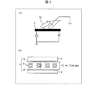
図2(a)は圧力センサ内蔵ディスプレイ1に設けられた自己容量型のタッチセンサ5のタッチパッド電極7の動作を説明するための図であり、(b)は圧力センサ内蔵ディスプレイ1に設けられた圧力センサ11の構成を模式的に示す断面図である。タッチパッド電極7は、図2(a)に示すように、検出対象である指16との間の容量又は容量変化を検出するように設けられる自己容量型の電極である。圧力センサ11は、図2(b)に示すように、回路基板2と対向基板3との間の液晶層4のセルギャップの変化に基づく圧力パッド電極12と駆動電極13との間の容量変化を検出する。
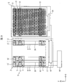
図3は、圧力センサ内蔵ディスプレイ1に設けられた回路基板2及び対向基板3の構成を示す模式図である。複数個のタッチパッド電極7及び複数個の圧力パッド電極12が回路基板2の上にマトリックス状に配置される。図3に示す例では、複数個の圧力パッド電極12が奇数行目に配置され、複数個のタッチパッド電極7が偶数行目に配置される。もちろん、逆に、複数個のタッチパッド電極7が奇数行目に配置され、複数個の圧力パッド電極12が偶数行目に配置されてもよい。
圧力パッド電極12は、液晶層4に含まれる液晶分子の配向を制御する電界を形成するための共通電極と共用される。タッチパッド電極7も共通電極と共用される。
タッチセンサ5は、各列に配置されたタッチパッド電極7のそれぞれに対応して列方向(Y軸方向)にそれぞれ延びる複数本のセンスライン6を有する。
このように、回路基板2には、液晶層4に含まれる液晶分子の配向を制御する電界を形成する複数の共通電極が電極アレイとしてマトリックス状に配置される。そして、当該電極アレイの一群が自己容量型のタッチパッド電極7としてタッチによる容量変化を検出する。また、当該電極アレイの残りの一群が相互容量型の圧力パッド電極12として駆動電極13と共に圧力による容量変化を検出する。
対向基板3には、複数本の駆動電極13が、圧力パッド電極12に対向して配置される。対向基板3は、周期的に配列して構成された三色のカラーフィルタ層を区画するために格子状に形成されたブラックマトリックス15を有する。そして、複数本の駆動電極13は、ブラックマトリックス15に形成される。三色のカラーフィルタ層はカラーフィルタを構成する。
このように、圧力検出のための送信電極(Tx)としての駆動電極13が、対向基板3のブラックマトリックス15の上にパターニングされる。そして、この送信電極は、回路基板2の上に配置された圧力検出のための受信電極(Rx)としての圧力パッド電極12と重なるようにパターニングされる。
回路基板2には、複数のタッチパッド電極7のそれぞれにセンスライン6を介して結合された自己容量コントローラ17と、各列に配置された圧力パッド電極12と1本の圧力センスライン20を介して結合された相互容量コントローラ18とが設けられる。自己容量コントローラ17及び相互容量コントローラ18はタイミング制御回路19に接続される。タイミング制御回路19は、液晶表示とタッチ検出と圧力検出とのタイミングと同期とを制御する。自己容量コントローラ17はディスプレイドライバに集積される。
対向基板3には、複数の駆動電極13と接続された相互容量コントローラ21が設けられる。相互容量コントローラ21は、回路基板2の相互容量コントローラ18に接続される。
(圧力センサ内蔵ディスプレイ1の動作)
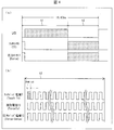
図4(a)は圧力センサ内蔵ディスプレイ1に設けられた液晶表示部とタッチセンサ5と圧力センサ11との動作を示すタイミングチャートであり、(b)は垂直ブランク期間における液晶表示部とタッチセンサ5と圧力センサ11との動作を示すタイミングチャートである。
図4(a)は圧力センサ内蔵ディスプレイ1に設けられた液晶表示部とタッチセンサ5と圧力センサ11との動作を示すタイミングチャートであり、(b)は垂直ブランク期間における液晶表示部とタッチセンサ5と圧力センサ11との動作を示すタイミングチャートである。
タッチセンサ5及び圧力センサ11は、液晶層4による表示の垂直同期に基づいて動作する。図4(a)に示すように、液晶層4(LCD)はディスプレイ書き込み期間t1において動作し、ディスプレイ書き込み期間t1に続く垂直ブランク期間t2にいて停止する。ディスプレイ書き込み期間t1と垂直ブランク期間t2の合計は16.67(ms、ミリ秒)である。タッチセンサ5による走査及び圧力センサ11による走査は、液晶層4による表示のリフレッシュ期間(垂直ブランク期間t2)に実行される。
タッチセンサ5は自己容量型であるため、個々のタッチパッド電極7は順番に充電され、そして放電する。圧力センサ11の送信電極(Tx)としての駆動電極13は、自己容量型のタッチセンサ5のタッチパッド電極7が充電される期間には、タッチ検出への悪影響を回避するために、電気的浮遊状態(フローティング状態)となる。
図5は、タッチセンサ5と圧力センサ11との動作の同期を説明するためのタイミングチャートである。まず、圧力センサイネーブル信号(Force TX enable)が時刻T1でロー状態(VL)からハイ状態(VH)に立ち上がると、圧力センサ11の送信電極(Tx)としての駆動電極13に印加される送信信号(Force Tx)もロー状態(VL)からハイ状態(VH)に立ち上がる。そして、圧力センサ11の受信電極としての圧力パッド電極12から読み出される読出信号(Force SH)が時刻T2においてロー状態(VL)からハイ状態(VH)に立ち上がる。次に、読出信号(Force SH)が時刻T3においてハイ状態(VH)からロー状態(VL)に立ち下がる。その後、時刻T4において圧力センサイネーブル信号(Force TX enable )及び送信信号(Force Tx)がハイ状態(VH)からロー状態(VL)に立ち下がる。
そして、タッチセンサ5のタッチパッド電極7に印加される送信信号(Touch Tx)が時刻T5においてロー状態(VL)からハイ状態(VH)に立ち上がる。次に、送信信号(Touch Tx)が時刻T6においてハイ状態(VH)からロー状態(VL)に立ち下がると、タッチセンサ5のタッチパッド電極7から読み出される読出信号(Touch SH)がロー状態(VL)からハイ状態(VH)に立ち上がる。その後、読出信号(Touch SH)が時刻T7においてハイ状態(VH)からロー状態(VL)に立ち下がる。そして、以下同様の動作が繰り返される。
圧力センサ11の送信電極(Tx)としての駆動電極13に印加される送信信号(Force Tx)は、図5に示すように、タッチセンサ5のタッチパッド電極7に印加される送信信号(Touch Tx)がハイ状態(VH)となる時刻T5から時刻T6までのセンシング期間t3において電気的浮遊状態(フローティング状態)となる。
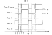
図6はタッチセンサ5と圧力センサ11との動作の他の同期を説明するためのタイミングチャートである。図5で前述した構成要素と同一の構成要素には同一の参照符号を付している。これらの構成要素の詳細な説明は繰り返さない。
タッチセンサ5のタッチパッド電極7に印加される送信信号(Touch Tx)が時刻T5においてロー状態(VL)からハイ状態(VH)に立ち上がるときに、圧力センサイネーブル信号(Force TX enable)もロー状態(VL)からハイ状態(VH)に立ち上がる。そして、送信信号(Touch Tx)が時刻T6においてハイ状態(VH)からロー状態(VL)に立ち下がるときに、圧力センサイネーブル信号(Force TX enable)もハイ状態(VH)からロー状態(VL)に立ち下がる。このように、送信信号(Touch Tx)は、タッチセンサ5の電極の上の寄生容量を低減するためのタッチセンシングの信号に類似した圧力センサイネーブル信号(Force TX enable)により駆動される。
図7(a)は圧力センサ11の動作を説明するための模式図であり、(b)はタッチセンサ5の動作を説明するための模式図である。センシング期間を効率的に使用するために圧力センシングとタッチセンシングとは連続して実施される。自己容量方式は充電期間と放電期間とが必要であるが、相互容量方式はセンシング期間を充電期間と放電期間とに分割する必要がない。圧力は、タッチセンサ5のタッチパッド電極7からの読出期間に検出することができる。タッチセンサ5のタッチパッド電極7の上の寄生容量を低減するために適切な方法を適用することにより、タッチパッド電極7に送信信号(Touch Tx)を印加する期間を低減して、タッチパッド電極7から読出信号(Touch SH)を読み出す期間及び圧力パッド電極12から読出信号(Force SH)を読み出す期間を長くすることができる。
圧力センシングの間は、図7(a)に示すように、回路基板2の上のすべての圧力パッド電極12が相互容量コントローラ18に接続される。そして、圧力センサ11の受信電極としての圧力パッド電極12からの信号が測定され、タッチパネル上の圧力が決定される。
タッチセンシングの間は、図7(b)に示すように、圧力センサ11の駆動電極13は電気的浮遊状態(フローティング状態)となる。圧力センサ11の圧力パッド電極12は、タッチパッド電極7上の負荷容量を低減してパフォーマンスを向上させるために、タッチパッド電極7の信号と類似した信号に結合される。
〔実施形態2〕
本発明の他の実施形態について、図8に基づいて説明すれば、以下のとおりである。なお、説明の便宜上、前記実施形態にて説明した部材と同じ機能を有する部材については、同じ符号を付記し、その説明を省略する。後続する実施形態も同様である。
本発明の他の実施形態について、図8に基づいて説明すれば、以下のとおりである。なお、説明の便宜上、前記実施形態にて説明した部材と同じ機能を有する部材については、同じ符号を付記し、その説明を省略する。後続する実施形態も同様である。
図8(a)は実施形態2に係る圧力センサ内蔵ディスプレイに設けられた回路基板2の構成を示す上面図であり、(b)は上記圧力センサ内蔵ディスプレイに設けられた対向基板3の構成を示す下面図である。
回路基板2には、各列に配置されたタッチパッド電極7及び圧力パッド電極12に対応してY方向(列方向)にそれぞれ延びる複数本のセンスライン6Aと、センスライン6Aと各タッチパッド電極7との間、及び、センスライン6Aと各圧力パッド電極12との間にそれぞれ形成される複数個のスイッチ素子8(第1スイッチ素子)が形成される。
回路基板2は、各行に配置された複数の圧力パッド電極12、及び、各行に配置された複数のタッチパッド電極7のそれぞれに駆動ライン24を介して接続された複数のマルチプレクサ25を有する。各マルチプレクサ25は走査回路26に接続される。複数個のスイッチ素子8を制御するためにX方向に延びる選択ライン23が走査回路26に接続される。
まず、駆動電極13に送信信号(Touch Tx)が印加されると、圧力パッド電極12のスイッチ素子8が選択ライン23を介して走査回路26によりオンになり、圧力パッド電極12からスイッチ素子8及びセンスライン6Aを通して読出信号(Force SH)が読み出される。そして、タッチパッド電極7に送信信号(Touch Tx)が駆動ライン24、マルチプレクサ25を介して走査回路26により印加される。次に、タッチパッド電極7のスイッチ素子8が選択ライン23を介して走査回路26によりオンになり、タッチパッド電極7からスイッチ素子8及びセンスライン6Aを通して読出信号(Touch SH)が読み出される。
〔実施形態3〕
図9(a)は実施形態3に係る圧力センサ内蔵ディスプレイに設けられた回路基板2の構成を示す上面図であり、(b)は上記圧力センサ内蔵ディスプレイに設けられた対向基板3の構成を示す下面図である。
図9(a)は実施形態3に係る圧力センサ内蔵ディスプレイに設けられた回路基板2の構成を示す上面図であり、(b)は上記圧力センサ内蔵ディスプレイに設けられた対向基板3の構成を示す下面図である。
圧力パッド電極12は2個のスイッチ素子8・9(第1スイッチ素子、第2スイッチ素子)を有する。スイッチ素子8は、Y方向に延びるセンスライン6Aに接続され、X方向に延びる選択ライン23を通して走査回路26Cにより制御される。
スイッチ素子9は、X方向に延びる駆動ライン24Cに接続され、X方向に延びる選択ライン23Cを通して走査回路26Cにより制御される。
〔まとめ〕
本発明の態様1に係る圧力センサ内蔵ディスプレイ1は、回路基板2と、前記回路基板2に対向して配置される対向基板3と、前記回路基板2と前記対向基板3との間に形成される表示層(液晶層4)と、前記対向基板3へのタッチを検出する静電容量型のタッチセンサ5と、前記対向基板3に加わる圧力を検出する圧力センサ11とを備え、前記タッチセンサ5が、前記回路基板2の前記表示層(液晶層4)側に配置される複数個のタッチパッド電極7を有し、前記圧力センサ11が、前記回路基板2の前記表示層(液晶層4)側に配置される複数個の圧力パッド電極12と、前記対向基板3の前記表示層(液晶層4)側に配置される複数本の駆動電極13とを有する。
本発明の態様1に係る圧力センサ内蔵ディスプレイ1は、回路基板2と、前記回路基板2に対向して配置される対向基板3と、前記回路基板2と前記対向基板3との間に形成される表示層(液晶層4)と、前記対向基板3へのタッチを検出する静電容量型のタッチセンサ5と、前記対向基板3に加わる圧力を検出する圧力センサ11とを備え、前記タッチセンサ5が、前記回路基板2の前記表示層(液晶層4)側に配置される複数個のタッチパッド電極7を有し、前記圧力センサ11が、前記回路基板2の前記表示層(液晶層4)側に配置される複数個の圧力パッド電極12と、前記対向基板3の前記表示層(液晶層4)側に配置される複数本の駆動電極13とを有する。
上記の構成によれば、タッチセンサのタッチパッド電極が回路基板の表示層側に配置される。そして、圧力センサの圧力パッド電極が回路基板の表示層側に配置され、圧力センサの駆動電極が対向基板の表示層側に配置される。このため、圧力センサとタッチセンサとがディスプレイに内蔵される。この結果、低コストでコンパクトな圧力センサ内蔵ディスプレイを実現することができる。
本発明の態様2に係る圧力センサ内蔵ディスプレイ1は、上記態様1において、前記複数個のタッチパッド電極7及び前記複数個の圧力パッド電極12がマトリックス状に配置され、前記複数個のタッチパッド電極7が奇数行目に配置され、前記複数個の圧力パッド電極12が偶数行目に配置されてもよい。
上記の構成によれば、タッチパッド電極と圧力パッド電極とを同一の製造工程により同時に形成することができる。
本発明の態様3に係る圧力センサ内蔵ディスプレイ1は、上記態様2において、前記複数本の駆動電極13が、前記偶数行目の圧力パッド電極12に対向して配置されてもよい。
上記の構成によれば、駆動電極と圧力パッド電極とにより相互容量型の圧力センサを構成することができる。
本発明の態様4に係る圧力センサ内蔵ディスプレイ1は、上記態様1から3のいずれか一態様において、前記表示層が液晶層4であり、前記圧力パッド電極12が、前記液晶層4に含まれる液晶分子の配向を制御する電界を形成するための共通電極と共用されてもよい。
上記の構成によれば、圧力パッド電極が共通電極と共用されるため、圧力センサ内蔵ディスプレイがより一層低コストでコンパクトになる。
本発明の態様5に係る圧力センサ内蔵ディスプレイ1は、上記態様1から4のいずれか一態様において、前記対向基板3が、三色のカラーフィルタ層を周期的に配列して構成されたカラーフィルタと、前記三色のカラーフィルタ層を区画するために格子状に形成されたブラックマトリックス15とを有し、前記複数本の駆動電極13が、前記ブラックマトリックス15に形成されてもよい。
上記の構成によれば、圧力センサの駆動電極が三色のカラーフィルタ層を区画するために格子状に形成されたブラックマトリックスに形成されるので、圧力センサ内蔵ディスプレイがより一層コンパクトになる。
本発明の態様6に係る圧力センサ内蔵ディスプレイ1は、上記態様2から5のいずれか一態様において、前記タッチセンサ5が、各列に配置されたタッチパッド電極7に対応して列方向にそれぞれ延びる複数本のセンスライン6・6Aと、前記センスライン6・6Aと各タッチパッド電極7との間にそれぞれ形成される複数個の第1スイッチ素子(スイッチ素子8)とをさらに有してもよい。
上記の構成によれば、第1スイッチ素子を設けることにより、列方向のタッチパッド電極から読出信号を1本のセンスラインで読み出すことができ、圧力センサ内蔵ディスプレイがより一層コンパクトになる。
本発明の態様7に係る圧力センサ内蔵ディスプレイ1は、上記態様2から6のいずれか一態様において、前記タッチセンサ5が、各行に配置されたタッチパッド電極7に対応して行方向にそれぞれ延びる複数本の駆動ライン24Cと、前記駆動ライン24Cと各タッチパッド電極7との間にそれぞれ形成される複数個の第2スイッチ素子(スイッチ素子9)とをさらに有してもよい。
上記の構成によれば、第2スイッチ素子を設けることにより、行方向のタッチパッド電極に送信信号を1本の駆動ラインで印加することができ、圧力センサ内蔵ディスプレイがより一層コンパクトになる。
本発明は上述した各実施形態に限定されるものではなく、請求項に示した範囲で種々の変更が可能であり、異なる実施形態にそれぞれ開示された技術的手段を適宜組み合わせて得られる実施形態についても本発明の技術的範囲に含まれる。さらに、各実施形態にそれぞれ開示された技術的手段を組み合わせることにより、新しい技術的特徴を形成することができる。
1 圧力センサ内蔵ディスプレイ
2 回路基板
3 対向基板
4 液晶層(表示層)
5 タッチセンサ
6 センスライン
7 タッチパッド電極
8 スイッチ素子(第1スイッチ素子)
9 スイッチ素子(第2スイッチ素子)
11 圧力センサ
12 圧力パッド電極(共通電極)
13 駆動電極
15 ブラックマトリックス
24 駆動ライン
2 回路基板
3 対向基板
4 液晶層(表示層)
5 タッチセンサ
6 センスライン
7 タッチパッド電極
8 スイッチ素子(第1スイッチ素子)
9 スイッチ素子(第2スイッチ素子)
11 圧力センサ
12 圧力パッド電極(共通電極)
13 駆動電極
15 ブラックマトリックス
24 駆動ライン
Claims (7)
- 回路基板と、
前記回路基板に対向して配置される対向基板と、
前記回路基板と前記対向基板との間に形成される表示層と、
前記対向基板へのタッチを検出する静電容量型のタッチセンサと、
前記対向基板に加わる圧力を検出する圧力センサとを備え、
前記タッチセンサが、前記回路基板の前記表示層側に配置される複数個のタッチパッド電極を有し、
前記圧力センサが、前記回路基板の前記表示層側に配置される複数個の圧力パッド電極と、前記対向基板の前記表示層側に配置される複数本の駆動電極とを有することを特徴とする圧力センサ内蔵ディスプレイ。 - 前記複数個のタッチパッド電極及び前記複数個の圧力パッド電極がマトリックス状に配置され、
前記複数個のタッチパッド電極が奇数行目に配置され、
前記複数個の圧力パッド電極が偶数行目に配置される請求項1に記載の圧力センサ内蔵ディスプレイ。 - 前記複数本の駆動電極が、前記偶数行目の圧力パッド電極に対向して配置される請求項2に記載の圧力センサ内蔵ディスプレイ。
- 前記表示層が液晶層であり、
前記圧力パッド電極が、前記液晶層に含まれる液晶分子の配向を制御する電界を形成するための共通電極と共用される請求項1から3の何れか一項に記載の圧力センサ内蔵ディスプレイ。 - 前記対向基板が、三色のカラーフィルタ層を周期的に配列して構成されたカラーフィルタと、前記三色のカラーフィルタ層を区画するために格子状に形成されたブラックマトリックスとを有し、
前記複数本の駆動電極が、前記ブラックマトリックスに形成される請求項1から4の何れか一項に記載の圧力センサ内蔵ディスプレイ。 - 前記タッチセンサが、各列に配置されたタッチパッド電極に対応して列方向にそれぞれ延びる複数本のセンスラインと、
前記センスラインと各タッチパッド電極との間にそれぞれ形成される複数個の第1スイッチ素子とをさらに有する請求項2から5の何れか一項に記載の圧力センサ内蔵ディスプレイ。 - 前記タッチセンサが、各行に配置されたタッチパッド電極に対応して行方向にそれぞれ延びる複数本の駆動ラインと、
前記駆動ラインと各タッチパッド電極との間にそれぞれ形成される複数個の第2スイッチ素子とをさらに有する請求項2から6の何れか一項に記載の圧力センサ内蔵ディスプレイ。
Priority Applications (2)
| Application Number | Priority Date | Filing Date | Title |
|---|---|---|---|
| CN201880022034.7A CN110462564A (zh) | 2017-03-29 | 2018-03-27 | 压力传感器内置显示器 |
| US16/496,465 US20200371626A1 (en) | 2017-03-29 | 2018-03-27 | Pressure-sensor-embedded display |
Applications Claiming Priority (2)
| Application Number | Priority Date | Filing Date | Title |
|---|---|---|---|
| JP2017065356 | 2017-03-29 | ||
| JP2017-065356 | 2017-03-29 |
Publications (1)
| Publication Number | Publication Date |
|---|---|
| WO2018181235A1 true WO2018181235A1 (ja) | 2018-10-04 |
Family
ID=63676186
Family Applications (1)
| Application Number | Title | Priority Date | Filing Date |
|---|---|---|---|
| PCT/JP2018/012276 Ceased WO2018181235A1 (ja) | 2017-03-29 | 2018-03-27 | 圧力センサ内蔵ディスプレイ |
Country Status (3)
| Country | Link |
|---|---|
| US (1) | US20200371626A1 (ja) |
| CN (1) | CN110462564A (ja) |
| WO (1) | WO2018181235A1 (ja) |
Families Citing this family (3)
| Publication number | Priority date | Publication date | Assignee | Title |
|---|---|---|---|---|
| GB2589974B (en) * | 2019-11-15 | 2022-01-26 | Clevetura Llc | Keyboard |
| CN112882593B (zh) * | 2019-11-29 | 2023-01-03 | 群创光电股份有限公司 | 触控电子装置的驱动方法 |
| US11741880B2 (en) * | 2020-09-02 | 2023-08-29 | Hefei Boe Optoelectronics Technology Co., Ltd. | Driving method, driving circuitry and display device |
Citations (3)
| Publication number | Priority date | Publication date | Assignee | Title |
|---|---|---|---|---|
| JP2010175595A (ja) * | 2009-01-27 | 2010-08-12 | Sony Corp | 液晶表示装置 |
| JP2010211541A (ja) * | 2009-03-10 | 2010-09-24 | Seiko Epson Corp | タッチセンサ機能付き表示装置 |
| JP2013508793A (ja) * | 2009-11-03 | 2013-03-07 | シャープ株式会社 | プレチャージ動作を用いるセンサ回路アレイを含む液晶デバイス |
Family Cites Families (2)
| Publication number | Priority date | Publication date | Assignee | Title |
|---|---|---|---|---|
| CN103150073B (zh) * | 2013-03-12 | 2015-10-14 | 合肥京东方光电科技有限公司 | 一种电容式内嵌触摸屏及显示装置 |
| CN106502444B (zh) * | 2015-09-03 | 2019-03-19 | 敦泰电子股份有限公司 | 触控显示装置及其驱动方法以及压力检测方法 |
-
2018
- 2018-03-27 US US16/496,465 patent/US20200371626A1/en not_active Abandoned
- 2018-03-27 WO PCT/JP2018/012276 patent/WO2018181235A1/ja not_active Ceased
- 2018-03-27 CN CN201880022034.7A patent/CN110462564A/zh active Pending
Patent Citations (3)
| Publication number | Priority date | Publication date | Assignee | Title |
|---|---|---|---|---|
| JP2010175595A (ja) * | 2009-01-27 | 2010-08-12 | Sony Corp | 液晶表示装置 |
| JP2010211541A (ja) * | 2009-03-10 | 2010-09-24 | Seiko Epson Corp | タッチセンサ機能付き表示装置 |
| JP2013508793A (ja) * | 2009-11-03 | 2013-03-07 | シャープ株式会社 | プレチャージ動作を用いるセンサ回路アレイを含む液晶デバイス |
Also Published As
| Publication number | Publication date |
|---|---|
| US20200371626A1 (en) | 2020-11-26 |
| CN110462564A (zh) | 2019-11-15 |
Similar Documents
| Publication | Publication Date | Title |
|---|---|---|
| JP6215640B2 (ja) | 静電容量式インセルタッチパネル及びディスプレイデバイス | |
| KR101418694B1 (ko) | 용량성 인-셀 터치 스크린 패널, 터치 포지셔닝 방법, 및 디스플레이 장치 | |
| JP4920245B2 (ja) | 感知素子を内装した液晶表示装置 | |
| US9529484B2 (en) | Capacitive touch structure using block electrodes to reduce wiring | |
| US9823789B2 (en) | Touch display panel and display device | |
| US10078239B2 (en) | Sensor-equipped display device | |
| EP3153915B1 (en) | Capacitive embedded touch panel, display device and drive method therefor | |
| US11093072B2 (en) | Touch display panel, method of driving and manufacturing same, and touch display device | |
| US9785276B2 (en) | Capacitive in-cell touch panel and display device | |
| TWI496044B (zh) | 觸控裝置、其觸控顯示器及其電子裝置 | |
| EP2602697A2 (en) | Display device with integrated touch screen | |
| EP3151098A1 (en) | Embedded touchscreen and display device | |
| TWI639938B (zh) | 觸控顯示面板 | |
| WO2014131248A1 (zh) | 电容式内嵌触摸屏及显示装置 | |
| WO2011139495A2 (en) | Integrated capacitive sensing and displaying | |
| TWI697822B (zh) | 觸控顯示方法與觸控顯示裝置 | |
| EP3118727B1 (en) | In-cell touchscreen and display device | |
| WO2016110045A1 (zh) | 内嵌式触摸屏及显示装置 | |
| EP3316237B1 (en) | Embedded touch control display screen and drive method therefor, and display device | |
| US10185423B2 (en) | Plug-in touch display device and an electronic device | |
| US20170060310A1 (en) | Touch sensor-integrated type display device | |
| KR20170026030A (ko) | 터치 디스플레이 장치와 이의 구동 방법 및 디스플레이 패널 | |
| WO2018181235A1 (ja) | 圧力センサ内蔵ディスプレイ | |
| CN108196723B (zh) | 显示面板 | |
| JPH09120334A (ja) | タブレット付液晶表示装置 |
Legal Events
| Date | Code | Title | Description |
|---|---|---|---|
| 121 | Ep: the epo has been informed by wipo that ep was designated in this application |
Ref document number: 18776679 Country of ref document: EP Kind code of ref document: A1 |
|
| NENP | Non-entry into the national phase |
Ref country code: DE |
|
| 122 | Ep: pct application non-entry in european phase |
Ref document number: 18776679 Country of ref document: EP Kind code of ref document: A1 |
|
| NENP | Non-entry into the national phase |
Ref country code: JP |