WO2018155196A1 - 受光装置 - Google Patents
受光装置 Download PDFInfo
- Publication number
- WO2018155196A1 WO2018155196A1 PCT/JP2018/004288 JP2018004288W WO2018155196A1 WO 2018155196 A1 WO2018155196 A1 WO 2018155196A1 JP 2018004288 W JP2018004288 W JP 2018004288W WO 2018155196 A1 WO2018155196 A1 WO 2018155196A1
- Authority
- WO
- WIPO (PCT)
- Prior art keywords
- pixel
- pixels
- amplifier
- unit
- unit element
- Prior art date
- Legal status (The legal status is an assumption and is not a legal conclusion. Google has not performed a legal analysis and makes no representation as to the accuracy of the status listed.)
- Ceased
Links
Images







Classifications
-
- H—ELECTRICITY
- H10—SEMICONDUCTOR DEVICES; ELECTRIC SOLID-STATE DEVICES NOT OTHERWISE PROVIDED FOR
- H10W—GENERIC PACKAGES, INTERCONNECTIONS, CONNECTORS OR OTHER CONSTRUCTIONAL DETAILS OF DEVICES COVERED BY CLASS H10
- H10W90/00—Package configurations
-
- G—PHYSICS
- G01—MEASURING; TESTING
- G01T—MEASUREMENT OF NUCLEAR OR X-RADIATION
- G01T1/00—Measuring X-radiation, gamma radiation, corpuscular radiation, or cosmic radiation
- G01T1/02—Dosimeters
- G01T1/10—Luminescent dosimeters
- G01T1/105—Read-out devices
-
- G—PHYSICS
- G01—MEASURING; TESTING
- G01T—MEASUREMENT OF NUCLEAR OR X-RADIATION
- G01T1/00—Measuring X-radiation, gamma radiation, corpuscular radiation, or cosmic radiation
- G01T1/16—Measuring radiation intensity
- G01T1/17—Circuit arrangements not adapted to a particular type of detector
-
- H—ELECTRICITY
- H04—ELECTRIC COMMUNICATION TECHNIQUE
- H04N—PICTORIAL COMMUNICATION, e.g. TELEVISION
- H04N23/00—Cameras or camera modules comprising electronic image sensors; Control thereof
- H04N23/30—Cameras or camera modules comprising electronic image sensors; Control thereof for generating image signals from X-rays
-
- H—ELECTRICITY
- H04—ELECTRIC COMMUNICATION TECHNIQUE
- H04N—PICTORIAL COMMUNICATION, e.g. TELEVISION
- H04N25/00—Circuitry of solid-state image sensors [SSIS]; Control thereof
- H04N25/70—SSIS architectures; Circuits associated therewith
- H04N25/76—Addressed sensors, e.g. MOS or CMOS sensors
-
- H—ELECTRICITY
- H10—SEMICONDUCTOR DEVICES; ELECTRIC SOLID-STATE DEVICES NOT OTHERWISE PROVIDED FOR
- H10F—INORGANIC SEMICONDUCTOR DEVICES SENSITIVE TO INFRARED RADIATION, LIGHT, ELECTROMAGNETIC RADIATION OF SHORTER WAVELENGTH OR CORPUSCULAR RADIATION
- H10F39/00—Integrated devices, or assemblies of multiple devices, comprising at least one element covered by group H10F30/00, e.g. radiation detectors comprising photodiode arrays
- H10F39/10—Integrated devices
- H10F39/12—Image sensors
-
- H—ELECTRICITY
- H10—SEMICONDUCTOR DEVICES; ELECTRIC SOLID-STATE DEVICES NOT OTHERWISE PROVIDED FOR
- H10F—INORGANIC SEMICONDUCTOR DEVICES SENSITIVE TO INFRARED RADIATION, LIGHT, ELECTROMAGNETIC RADIATION OF SHORTER WAVELENGTH OR CORPUSCULAR RADIATION
- H10F39/00—Integrated devices, or assemblies of multiple devices, comprising at least one element covered by group H10F30/00, e.g. radiation detectors comprising photodiode arrays
- H10F39/10—Integrated devices
- H10F39/12—Image sensors
- H10F39/18—Complementary metal-oxide-semiconductor [CMOS] image sensors; Photodiode array image sensors
- H10F39/189—X-ray, gamma-ray or corpuscular radiation imagers
-
- H—ELECTRICITY
- H10—SEMICONDUCTOR DEVICES; ELECTRIC SOLID-STATE DEVICES NOT OTHERWISE PROVIDED FOR
- H10F—INORGANIC SEMICONDUCTOR DEVICES SENSITIVE TO INFRARED RADIATION, LIGHT, ELECTROMAGNETIC RADIATION OF SHORTER WAVELENGTH OR CORPUSCULAR RADIATION
- H10F39/00—Integrated devices, or assemblies of multiple devices, comprising at least one element covered by group H10F30/00, e.g. radiation detectors comprising photodiode arrays
- H10F39/80—Constructional details of image sensors
- H10F39/802—Geometry or disposition of elements in pixels, e.g. address-lines or gate electrodes
-
- H—ELECTRICITY
- H10—SEMICONDUCTOR DEVICES; ELECTRIC SOLID-STATE DEVICES NOT OTHERWISE PROVIDED FOR
- H10F—INORGANIC SEMICONDUCTOR DEVICES SENSITIVE TO INFRARED RADIATION, LIGHT, ELECTROMAGNETIC RADIATION OF SHORTER WAVELENGTH OR CORPUSCULAR RADIATION
- H10F39/00—Integrated devices, or assemblies of multiple devices, comprising at least one element covered by group H10F30/00, e.g. radiation detectors comprising photodiode arrays
- H10F39/80—Constructional details of image sensors
- H10F39/803—Pixels having integrated switching, control, storage or amplification elements
-
- H—ELECTRICITY
- H10—SEMICONDUCTOR DEVICES; ELECTRIC SOLID-STATE DEVICES NOT OTHERWISE PROVIDED FOR
- H10F—INORGANIC SEMICONDUCTOR DEVICES SENSITIVE TO INFRARED RADIATION, LIGHT, ELECTROMAGNETIC RADIATION OF SHORTER WAVELENGTH OR CORPUSCULAR RADIATION
- H10F39/00—Integrated devices, or assemblies of multiple devices, comprising at least one element covered by group H10F30/00, e.g. radiation detectors comprising photodiode arrays
- H10F39/80—Constructional details of image sensors
- H10F39/813—Electronic components shared by multiple pixels, e.g. one amplifier shared by two pixels
Definitions
- the present technology relates to a light receiving device, for example, a light receiving device suitable for application to a device that detects radiation such as ⁇ rays, ⁇ rays, ⁇ rays, or X rays.
- Patent Document 1 describes a back-illuminated imaging device as an example of an imaging device having such a photoelectric conversion element.
- Patent Document 2 a radiation imaging apparatus is proposed as an example of an imaging apparatus having a photoelectric conversion element.
- an active light receiving device in which an amplifier circuit is built in a pixel is required.
- noise can be reduced.
- Sensitivity is also an important factor. Increasing sensitivity and reducing noise leads to reduced exposure.
- the radiation imaging device requires a size that matches the size of each part of the human body to be imaged. The maximum size is required to be 40 cm ⁇ 30 cm or more, for example. Therefore, a technique for enlarging a high-performance sensor is also necessary.
- an output line is formed for each column and is read simultaneously in the vertical direction.
- a low noise light receiving device active type
- a circuit in the vicinity of the pixel.
- the fill factor may be suppressed by the circuit area and the light receiving sensitivity may be reduced.
- the resolution and the light receiving sensitivity are in a trade-off relationship depending on the pixel area and the circuit area.
- the readout is simple but it is difficult to realize a global shutter due to problems with dynamic range and linearity.
- an image sensor having a structure in which an IC element is stacked and an amplifier is shared by a plurality of photoelectric conversion elements has been proposed.
- the pixel readout sequence becomes zigzag, and it is necessary to rearrange the numerical values after readout, which may complicate the sequence.
- the present technology has been made in view of such a situation, and even when a shared structure in which an amplifier is shared by a plurality of pixels is used, processing after readout can be prevented from becoming complicated. To do.
- a light receiving element includes a plurality of pixels arranged in m rows and n columns, and a reading unit that sequentially reads signals from the plurality of pixels arranged in the column direction among the plurality of pixels.
- a plurality of unit elements are arranged on the substrate, and the number of the reading units is at least the same as the number of columns.
- the light receiving element includes a plurality of pixels arranged in m rows and n columns, and a reading unit that sequentially reads signals from the plurality of pixels arranged in the column direction among the plurality of pixels.
- a plurality of unit elements are arranged on the substrate. Further, the number of reading units is at least the same as the number of columns.
- the light receiving device may be an independent device or an internal block constituting one device.
- FIG. 10 is a diagram for describing a structure of a transistor. It is a figure for demonstrating noise reduction.
- the present technology can be applied to an apparatus that detects radiation such as ⁇ rays, ⁇ rays, ⁇ rays, or X rays. Further, such a device can be applied to a light receiving device that receives light by radiation.
- FIG. 1 is a block diagram illustrating a configuration example of an embodiment of a radiation imaging apparatus including a light receiving device to which the present technology is applied.
- the radiation imaging apparatus includes a radiation detector, a CT apparatus, a line sensor, and the like.
- the radiation imaging apparatus 10 irradiates an object O (a person in the example of FIG. 1) on the imaging table 12 with X-rays to capture an image.
- the arm 11 of the radiation imaging apparatus 10 includes an MPU (Micro Processing Unit) (not shown) and various processing circuits inside, and controls the multipoint parallel X-ray source 13.
- the arm 11 holds the imaging table 12, the multipoint parallel X-ray source 13, the shield plate 14, and the imaging unit 15.
- the imaging table 12 is a table on which the subject O is placed.
- the multi-point parallel X-ray source 13 has, for example, a plurality of X-ray tubes and a plurality of collimators, and emits parallel beam X-rays to the imaging table 12 under the control of the arm 11.
- the shield plate 14 is made of a metal capable of blocking X-rays such as lead and iron, and is provided between the multipoint parallel X-ray source 13 and the imaging table 12.
- the subject O is placed between the photographing stand 12 and the shield plate 14.
- the shield plate 14 is provided with an opening 14A, and X-rays emitted from the multipoint parallel X-ray source 13 are applied to the subject O through the opening 14A. Accordingly, the subject O is placed on the photographing stand 12 so that the position of the opening 14A corresponds to the position of the photographing target.
- the imaging unit 15 has an X-ray CMOS image sensor, converts X-rays irradiated from the multipoint parallel X-ray source 13 through the opening 14A into visible light, and images the image.
- the imaging unit 15 holds an image obtained as a result, or transmits the image to another device via a network (not shown).
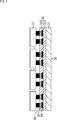
- FIG. 2 is a cross-sectional view showing the configuration of the light receiving device of the photographing unit 15 in FIG.
- the light receiving device 30 shown in FIG. 2 detects radiation such as ⁇ rays, ⁇ rays, ⁇ rays, or X rays, and can be used as an indirect conversion type radiation detector.
- the indirect conversion method refers to a method of converting radiation into visible light after converting radiation into visible light.
- the light receiving device 30 includes a substrate 31, an insulating film 32, an insulating film 33, a wiring layer 34, a UBM (Under Barrier Metal) 35, a solder layer 36, and a unit element 37.
- the layer 36 is a wiring board 38.
- the substrate 31 is made of, for example, glass, quartz, an organic substrate, etc., and a plurality of unit elements 37 are formed and connected thereto, and are connected to terminals of a power source, a ground, and a reference power source arranged side by side, for example. It also has wiring for extracting the signal to the outside.
- the wiring arranged in the horizontal direction is a wiring for supplying various control signals.
- a plurality of unit elements 37 are mounted on a wiring board 38 via a UBM 35 and a solder layer 36.
- the unit element 37 can be made of silicon.
- FIG. 3 shows an example in which nine unit elements 37 of the unit elements 37-1 to 37-9 are arranged.
- the imaging unit 15 of the radiation imaging apparatus 10 illustrated in FIG. 1 is sized according to the size of each part of the human body to be imaged, the imaging unit 15 is configured to have a size of about 40 cm ⁇ 30 cm, for example.
- the unit element 37 may be formed in a size of about 40 cm ⁇ 30 cm, but it is difficult to form the unit element 37 in this size because the strength cannot be maintained. Therefore, for example, a case where the unit element 37 is formed in a size that can maintain the strength and the plurality of unit elements 37 are arranged on the substrate 31 to form the imaging unit 15 of about 40 cm ⁇ 30 cm is taken as an example. Continue to explain.
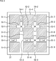
- One unit element 37 has a configuration as shown in FIG.
- the unit element 37 shown in FIG. 4 is a plan view when viewed from the substrate 31 side.
- the unit element 37 shown in FIG. 4 is configured to include nine 3 ⁇ 3 pixels 51.
- 1 unit element 37 includes a plurality of pixels 51, and the number of pixels 51 included in one unit element 37 is not limited to nine.
- the description will be continued by taking as an example a case where nine pixels 51 are included in one unit element 37, but the present technology is not limited to nine and may be applied to a unit element 37 including a plurality of pixels 51. .
- M is 3 or more
- n is 2 or more, that is, the number of pixels arranged in the vertical direction (vertical direction) is 3 or more, and the number of pixels arranged in the horizontal direction (horizontal direction) is The present technology is applied when the number is two or more.
- the unit element 37 shown in FIG. 4 includes buffers 52-1 to 52-3, constant current supply units (Iref) 53-1 to 53-3, and a decoder 54-1. To 54-3, and QV amplifiers 55-1 to 55-3.
- the pixels 51-1 to 51-9 are simply referred to as pixels 51 when it is not necessary to distinguish them individually. Moreover, it describes similarly about another part.
- the pixel 51 is configured to include a photodiode and receives incident light.
- the buffer 52 temporarily holds a signal indicating the amount of charge accumulated in the pixel 51 read out via the QV amplifier 55 and outputs the signal to a subsequent processing unit (not shown).
- the QV amplifier 55 is a charge-voltage conversion amplifier and includes a conversion circuit that converts the photocurrent from the pixel 51 into a voltage signal, and performs processing such as selection of the pixel 51 that reads the photocurrent and resetting of the pixel 51. Do.
- the decoder 54 controls the operation of the QV amplifier 55.
- the constant current supply unit 53 converts the supplied current and voltage into a stabilized current and voltage, and supplies the converted current and voltage to each unit of the unit element 37.
- the unit element 37 includes a plurality of pixels 51 and a reading unit that reads signals from the pixels 51, and the reading unit includes a QV amplifier 55 that includes a conversion circuit that converts a photocurrent from the pixels 51 into a voltage signal;
- the buffer 52 connected to the output side of the conversion circuit is included.
- the unit element 37 includes a decode 54 for controlling the reading unit.
- the unit element 37 shown in FIG. 4 has three pixels 51 that share one buffer 52, constant current supply unit 53, decoder 54, and QV amplifier 55.
- the buffer 52 When not sharing, since the buffer 52, the constant current supply unit 53, the decoder 54, and the QV amplifier 55 are provided for each pixel 51, when the size of the unit element 37 is limited, the buffer 52, There is a possibility that the area for arranging the constant current supply unit 53, the decoder 54, and the QV amplifier 55 becomes large, and the area of the pixel 51 becomes small. Therefore, there is a possibility that the sensitivity is lowered.
- the three pixels 51 share the buffer 52, constant current supply unit 53, decoder 54, and QV amplifier 55. It is possible to reduce the number of buffers 52, constant current supply units 53, decoders 54, and QV amplifiers 55 that are indispensable. By reducing these numbers, the area of the pixel 51 can be enlarged. Therefore, the sensitivity can be improved (maintained).
- the number of buffers 52, constant current supply units 53, decoders 54, and QV amplifiers 55 that must be arranged in the unit element 37 is reduced, so that the unit elements 37 in the unit element 37 that can be assigned to one of them are arranged. It is also possible to enlarge the area. Further, by sharing the buffer 52, the constant current supply unit 53, the decoder 54, and the QV amplifier 55, the number of terminals that must be provided on the substrate 31 can be reduced. Effects such as improvement of noise and reduction of noise can also be obtained.
- the pixel 51-1, the pixel 51-2, and the pixel 51-3 arranged in the vertical direction include a buffer 52-1, a constant current supply.
- the unit 53-1, the decoder 54-1, and the QV amplifier 55-1 are shared.
- the pixel 51-4, the pixel 51-5, and the pixel 51-6 arranged in the vertical direction include a buffer 52-2, a constant current supply unit 53-2, and a decoder. 54-2 and the QV amplifier 55-2 are shared.
- the pixel 51-7, the pixel 51-8, and the pixel 51-9 arranged in the vertical direction include a buffer 52-3, a constant current supply unit 53-3, and a decoder. 54-3 and the QV amplifier 55-3 are shared.
- the plurality of pixels 51 arranged in the vertical direction share the buffer 52, the constant current supply unit 53, the decoder 54, and the QV amplifier 55, so that signals from the pixels 51 in the vertical direction can be obtained. Can be read sequentially. This will be described with reference to FIG.
- FIG. 5 is a diagram showing only the pixel 51 and the QV amplifier 55 in the unit element 37 shown in FIG.
- the QV amplifier 55A-1 reads the signal from the pixel 51A-1, and then in the vertical direction of the pixel 51A-1.
- a signal from the pixel 51A-2 disposed on the lower side is read out, and then a signal from the pixel 51A-3 disposed on the lower side in the vertical direction of the pixel 51A-2 is read out.
- the QV amplifier 55A-2 reads out the signal from the pixel 51A-4, and then reads out the signal from the pixel 51A-5 arranged on the lower side in the vertical direction of the pixel 51A-4. Next, a signal from the pixel 51A-6 disposed on the lower side in the vertical direction of the pixel 51A-5 is read out.
- the QV amplifier 55A-3 reads a signal from the pixel 51A-7, and then reads a signal from the pixel 51A-8 arranged on the lower side in the vertical direction of the pixel 51A-7. Next, a signal from the pixel 51A-9 arranged on the lower side in the vertical direction of the pixel 51A-8 is read out.
- signals are sequentially read from the pixels 51 arranged in the vertical direction.
- processing such as replacement of signals (numerical values) in the subsequent processing, and simplifies the processing in the subsequent processing. Is possible.
- the QV amplifier 55A-1 is shared by the pixel 51A-1, the pixel 51A-2, the pixel 51A-4, and the pixel 51A-5 for comparison.
- the QV amplifier 55A-1 is shared by the 2 ⁇ 2 pixels 51A.
- the QV amplifier 55A-1 reads out signals in the order of the pixel 51A-1, the pixel 51A-4, the pixel 51A-2, and the pixel 51A-5.
- the pixel reading sequence becomes zigzag, and numerical value rearrangement is required during processing after reading, which may complicate the sequence.
- the pixel readout sequence can be a sequence that can be read out only in the vertical direction, and it is not necessary to rearrange numerical values during processing, and the sequence becomes complicated. It becomes possible to prevent this.
- the QV amplifier 55 includes 4 ⁇ 2 pixels 2 ⁇ 2 and is arranged in a portion that becomes a trap in such an arrangement.
- ⁇ In general, it means a road that crosses in a cross shape.
- the word “ ⁇ ” is used to mean a portion (area) where the road intersects.
- the heel is an area including a central portion of an area where 2 ⁇ 2 four pixels 51 are arranged, and is an area other than the pixels 51.
- the QV amplifier 55-1 is disposed in the heel portion composed of the pixel 51-1, the pixel 51-2, the pixel 51-4, and the pixel 51-5.
- the QV amplifier 55-2 is disposed in the heel portion composed of the pixel 51-4, the pixel 51-5, the pixel 51-7, and the pixel 51-8.
- the QV amplifier 55-3 is disposed in the heel portion composed of the pixel 51-5, the pixel 51-6, the pixel 51-8, and the pixel 51-9.
- the QV amplifier 55 is arranged in the heel portion constituted by arranging the 2 ⁇ 2 four pixels 51.
- the part that becomes the ridge becomes an area wider than an area (road) formed between the pixels 51.
- the QV amplifier 55 is arranged in such a wide area.
- the QV amplifier 55 includes a plurality of transistors inside, the circuit scale tends to increase. Therefore, it is possible to efficiently arrange the QV amplifier 55 in the unit element 37 by disposing such a QV amplifier 55 in a portion that becomes a flange.
- circuits other than the QV amplifier 55 such as the buffer 52, the constant current supply unit 53, and the decoder 54 are arranged in the region between the pixels 51 (region corresponding to the road). It becomes possible to do. Therefore, it is possible to increase the area allocated to circuits other than the QV amplifier 55.
- FIG. 6 shows an example in which 16 pixels 51B of 4 ⁇ 4 are arranged.
- the QV amplifier 55B-1 is arranged in a heel portion composed of 4 ⁇ 2 pixels, that is, the pixel 51B-1, the pixel 51B-2, the pixel 51B-5, and the pixel 51B-6.
- the QV amplifier 55B-1 is shared by the pixel 51B-1, the pixel 51B-2, the pixel 51B-3, and the pixel 51B-4 arranged in the vertical direction.
- the QV amplifier 55B-1 reads out signals in the order of the pixel 51B-1, the pixel 51B-2, the pixel 51B-3, and the pixel 51B-4 arranged in the vertical direction.
- the QV amplifier 55B-2 is arranged in a heel portion composed of 4 ⁇ 2 pixels, that is, the pixel 51B-2, the pixel 51B-3, the pixel 51B-6, and the pixel 51B-7.
- the QV amplifier 55B-2 is shared by the pixels 51B-5, 51B-6, 51B-7, and 51B-8 arranged in the vertical direction.
- the QV amplifier 55B-2 reads out signals in the order of the pixel 51B-5, the pixel 51B-6, the pixel 51B-7, and the pixel 51B-8 arranged in the vertical direction.
- the QV amplifier 55B-3 is disposed in the heel portion composed of 2 ⁇ 2 4 pixels of the pixel 51B-9, the pixel 51B-10, the pixel 51B-13, and the pixel 51B-14.
- the QV amplifier 55B-3 is shared by the pixel 51B-9, the pixel 51B-10, the pixel 51B-11, and the pixel 51B-12 arranged in the vertical direction.
- the QV amplifier 55B-3 reads signals in the order of the pixel 51B-9, the pixel 51B-10, the pixel 51B-11, and the pixel 51B-12 arranged in the vertical direction.
- the QV amplifier 55B-4 is disposed in the heel portion composed of 2 ⁇ 2 4 pixels of the pixel 51B-10, the pixel 51B-11, the pixel 51B-14, and the pixel 51B-15.
- the QV amplifier 55B-4 is shared by the pixels 51B-13, 51B-14, 51B-15, and 51B-16 arranged in the vertical direction.
- QV amplifier 55B-4 reads signals in the order of pixel 51B-13, pixel 51B-14, pixel 51B-15, and pixel 51B-16 arranged in the vertical direction.
- the QV amplifier 55B is shared so that signals are sequentially read from the pixels 51B arranged in the vertical direction (column direction). By doing so, it is possible to simplify the sequence after signal reading.
- the arrangement position of the QV amplifier 55B shown in FIG. 6 is an example, and does not indicate limitation.
- the QV amplifier 55B-2 is composed of 2 ⁇ 2 pixels, ie, a pixel (pixel 51B-5, pixel 51B-6, pixel 51B-9, and pixel 51B-10) on the right side of the QV amplifier 55B-1. You may comprise in the part of ⁇ ).
- the QV amplifier 55B-2 is connected to the next lower collar (pixel 51B-3, pixel 51B-4, pixel 51B-7, and pixel 51B-8 2 ⁇ ) below the QV amplifier 55B-1.
- it may be constructed in the part of ii) composed of 2 4 pixels.
- the QV amplifier 55B may be formed in the adjacent ridge portion, or may be formed in the ridge portion spaced apart.
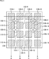
- the unit element 37C shown in FIG. 7 shows an example in which six 2 ⁇ 3 pixels 51C are arranged.
- the QV amplifier 55C-1 is arranged in a heel portion composed of 2 ⁇ 2 four pixels of the pixel 51C-1, the pixel 51C-2, the pixel 51C-4, and the pixel 51C-5.
- the QV amplifier 55C-1 is shared by the pixel 51C-1, the pixel 51C-2, and the pixel 51C-3 arranged in the vertical direction.
- the QV amplifier 55C-1 reads signals in the order of the pixel 51C-1, the pixel 51C-2, and the pixel 51C-3 arranged in the vertical direction.
- the QV amplifier 55C-2 is disposed in a heel portion composed of 4 ⁇ 2 pixels, that is, the pixel 51C-2, the pixel 51C-3, the pixel 51C-5, and the pixel 51C-6.
- the QV amplifier 55C-2 is shared by the pixel 51C-4, the pixel 51C-5, and the pixel 51C-6 arranged in the vertical direction.
- the QV amplifier 55C-2 reads signals in the order of the pixel 51C-4, the pixel 51C-5, and the pixel 51C-6 arranged in the vertical direction.
- the QV amplifier 55C is shared so that signals can be sequentially read from the pixels 51C arranged in the vertical direction (column direction) also in the unit element 37C including the 6 pixels 51C of 2 ⁇ 3. By doing so, it is possible to simplify the sequence after signal reading.
- the present technology when the same number of pixels 51 are arranged in the row direction and the column direction (horizontal direction and vertical direction) as in the unit element 37A shown in FIG. 5 and the unit element 37B shown in FIG.
- the present invention can also be applied, and can also be applied to the case where different numbers of pixels 51 are arranged in the row direction and the column direction (horizontal direction and vertical direction) as in the unit element 37C shown in FIG.
- the present technology can also be applied to the unit element 37 having the number of pixels 51 not shown in FIGS.
- the positions of the QV amplifiers 55A to 55C exemplified in the unit elements A to C shown in FIG. 5 to FIG. 7 are an example, and are not a limitation.
- the QV amplifier 55A-2 is provided below the QV amplifier 55A-1, in other words, the pixel 51A-2, the pixel 51A-3, the pixel 51A-5, and the pixel 51A. It may be placed in the heel part composed of -6.
- the number of QV amplifiers 55 in one unit element 37 is equal to the number of columns of the pixels 51 arranged in the unit element 37.
- the unit element 37A shown in FIG. 5 has three QV amplifiers 55A because the pixels 51A are arranged in three rows and three columns.
- the unit element 37B shown in FIG. 6 has four QV amplifiers 55B because the pixels 51B are arranged in four rows and four columns.
- the unit element 37C shown in FIG. 7 has two QV amplifiers 55C because the pixels 51C are arranged in three rows and two columns.
- the same number of QV amplifiers 55 as the number of columns of the pixels 51 arranged in the unit element 37 are arranged in the ridge portion in the unit element 37.
- the ridge portion is a portion where an anode and a cathode are not formed and has a large area. The design efficiency is very good, and the QV amplifier 55 is arranged in such a region.
- the description will be continued with an example in which the same number of QV amplifiers 55 as the number of columns of the pixels 51 arranged in the unit element 37 are arranged in the ridge portion in the unit element 37.
- the QV amplifiers 55 having a larger number than the number of columns of the pixels 51 may be provided.
- a QV amplifier 55 that reads out the pixels 51 for five rows is provided for each column, and in the unit element 37, six QV amplifiers are provided. 55 may be arranged.
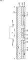
- FIG. 8 shows a cross-sectional view of the unit element 37.
- the cross-sectional view of the unit element 37 shown in FIG. 8 is, for example, a cross-sectional view taken along the line segment AA ′ shown at the pixel 51C-3 and the pixel 51C-5 of the unit element 37C of FIG. .
- the pixel 51C-2 and the pixel 51C-5 have a configuration in which a P ⁇ layer 101, a P ⁇ layer 102, a P ++ layer 103, and a circuit area 104 are stacked in this order from the light receiving unit side.
- the P + layer 105 is provided in the same layer as the circuit area 104.
- a cathode 106 is formed on the side of the P + layer 105.
- a separation layer including a P ++ layer 107 and a P ++ layer 108 is formed between the pixel 51C-2 and the pixel 51C-5 (between the cathodes 106).
- the circuit area 104 and the cathode 106 exist on the same plane, and an amplifier is formed inside the pixel.
- an amplifier is formed inside the pixel.
- the shape of the cathode 106 is a ring shape, is discrete (like a floating island), or a combination thereof.
- the circuit is inserted into the gap between the cathodes 106.
- a circuit is formed on the surface type (electrode side).
- high-concentration impurities are diffused in the epi layer.
- the portion where the QV amplifier 55 is disposed is the widest region of the P + layer 108, so that the design efficiency is very excellent.
- a circuit other than the QV amplifier 55 can be designed at the P + layer 108.
- FIG. 9 is a diagram illustrating a circuit configuration of the unit element 37. 9, an example in which the QV amplifier 55 and the like are shared by the three pixels 51 shown in FIG. 4 will be described.
- the pixels 51-1 to 51-3 are connected to the negative terminal side of the QV amplifier 55-1 via switches 152-1 to 152-3 that adjust the readout timing, respectively.
- a capacitor 151-1 is connected in parallel to the pixel 51-1.
- a capacitor 151-2 is connected in parallel to the pixel 51-2, and a capacitor 151-3 is connected in parallel to the pixel 51-3.
- the switch 152-1 is a timing adjustment switch for moving a signal from the pixel 51-1 (photodiode) to the QV amplifier 55-1.
- the switch 152-2 is a timing adjustment switch for moving a signal from the pixel 51-2 (photodiode) to the QV amplifier 55-1, and the switch 152-3 is the pixel 51-3 (photodiode). This is a switch for timing adjustment for moving a signal to the QV amplifier 55-1.
- the reference voltage Vref is supplied from the reference power source to the + terminal side of the QV amplifier 55-1.
- The-terminal and the output terminal of the QV amplifier 55-1 are connected via a capacitor 153 that stores photocharges.
- a transistor 154 for resetting the capacitor 153 is connected to both ends of the capacitor 153.
- the QV amplifier 55-1 performs IV conversion (current-voltage conversion).
- the output from the QV amplifier 55-1 is supplied to the + terminal of the buffer 52-2.
- The-terminal of the buffer 52-2 is connected to the output terminal of the buffer 52-2.
- the output terminal of the buffer 52-2 is connected to a transistor 155 for adjusting the output timing. By this transistor 155, a signal once held in the buffer 52-2 is processed in a subsequent processing unit (not shown). Are output at a predetermined timing.
- the buffer 52-2 is provided to output with low impedance because of the long wiring length.
- the switch 152-1 is closed, and a signal is transferred from the pixel 51-1 to the QV amplifier 55-1. After transfer, switch 152-1 is opened.
- the signal from the pixel 51-1 is processed after the QV amplifier 55-1, and the switch 152-2 is closed at time t2, and the signal is transferred from the pixel 51-2 to the QV amplifier 55-1. Is done. After transfer, switch 152-2 is opened.
- the signal from the pixel 51-2 is processed after the QV amplifier 55-1, and at the time t3, the switch 152-3 is closed, and the signal from the pixel 51-3 to the QV amplifier 55-1 is transmitted. Is transferred. After transfer, switch 152-3 is opened.
- the pixels 51-1 to 51-3 are the pixels 51 arranged in the column direction (vertical direction) as shown in FIG. In this way, signals from the pixels 51 arranged in the column direction are sequentially read out by the shared QV amplifier 55.
- FIG. 10 is a diagram illustrating an example of wirings and terminals formed on the substrate 31.
- the wirings and terminals shown in FIG. 10 are wirings and terminals for one unit element 37, and wirings and terminals for a plurality of unit elements 37 connected to the substrate 31 are formed on the substrate 31.
- Various power sources and output lines are formed on the substrate 31 in the vertical direction (vertical direction) in the figure, and various control lines are formed in the horizontal direction (horizontal direction) in the figure.
- a Vref signal line 201, an OUT1 signal line 202, a Vcc signal line 203, and a Gnd signal line 204 are formed as various power sources and output lines.
- As various control lines a D0 control line 205, a D1 control line 206, a D2 control line 207, a D3 control line 208, a D4 control line 209, a Gain control line 210, and a BIN control line 211 are formed.
- the BIN terminal 231, Vcc terminal 232, GND terminal 233, D4 terminal 234, Gain terminal 235, NC terminal 236, D2 terminal 237, D3 terminal 238, D0 terminal 239, OUT1 terminal 240, and D1 terminal 241 Is formed.
- the QV amplifier 55 is not shared by a plurality of pixels 51, the BIN terminals 231 to D1 terminals 241 are provided for each pixel 51.
- the terminals can be shared by the plurality of pixels 51, so that the number of terminals required for one unit element 37 can be reduced.
- FIG. 11 is a diagram showing another example of wirings and terminals formed on the substrate 31.
- the substrate 31 shown in FIG. 11 is different from the substrate 31 shown in FIG. 10 in that an output line is added.
- the substrate 31 shown in FIG. 10 shows the case where the output line is one of the OUT1 signal lines 202, but the substrate 31 shown in FIG. 11 has the output lines of the OUT1 signal line 202 and the OUT2 signal line 251. And three OUT3 signal lines 252 are formed. In addition, an OUT2 terminal 271 and an OUT3 terminal 272 are added as terminals connected to these signal lines. By using three OUT lines, the time required for output can be shortened.
- the number of terminals required for one unit element 37 can be reduced as in the case of the substrate 31 shown in FIG. 10.
- the number of terminals does not increase so much even if the number of pixels 51 sharing the QV amplifier 55 and the like increases.
- the QV amplifier 55 and the like are not illustrated, but the QV amplifier 55 is shared by the pixels 51-1 to 51-4.
- Terminals such as D0 to D4 terminals are connected to signal lines for transmitting 0 or 1 signals.
- FIG. 12 when the four terminals D0 to D3 are provided, the operation of 4 items in 2 is possible.
- FIG. 10 when five terminals, D0 to D4, are provided, the operation of 5 items of 2 is possible.
- double operation becomes possible by increasing the D terminal by one.
- the number of terminals can be reduced by adopting the shared pixel configuration.
- the distance between the bumps is shortened, the possibility that the bumps come into contact with each other increases. Since the distance between the terminals can be increased, the possibility that the bumps come into contact with each other can be reduced.
- the distance between the bumps can be increased, the possibility of contact with other bumps can be reduced even if the bump itself is enlarged.
- the connection between the terminal and the bump can be made stronger.
- the reliability of the light receiving device 30 can be improved by reducing the number of terminals and keeping the distance between the terminals.
- the light receiving device 30 When the light receiving device 30 is applied to a device that detects radiation such as ⁇ -rays, ⁇ -rays, ⁇ -rays, or X-rays, it is necessary to consider that it is affected by the radiation. When a large amount of radiation is incident, it is caused by the ionizing action, and the generated charge forms a fixed charge or an interface state, thereby deteriorating the characteristics of the device. For example, it becomes a leak source between transistors. Since the QV amplifier 55 and the like include a plurality of transistors, it is preferable to remove a leak source between the transistors.
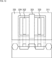
- FIG. 13A and 13B are a plan view and a cross-sectional view of the transistor 311.
- the transistor 311 includes a gate 321, a source 322, and a drain 323.
- a LOCOS (Local Oxidation of Silicon) portion 325 for element isolation is formed on the outer periphery of the transistor 311.
- an offset portion 324 is formed between the source 322 (drain 323) and the LOCOS portion 325. By providing such an offset portion 324, leakage from the LOCOS portion 325 can be prevented.
- the offset portion 324 may be formed by increasing the concentration by ion implantation of boron (B) to improve the isolation characteristics between transistors.
- a configuration in which leakage is prevented may be achieved by increasing the distance between the source 322 and the drain 323 by forming the transistor in a ring shape.
- the influence of the leak can be reduced.
- the offset portion 324 is provided as in the configuration of the transistor 311 illustrated in FIG. 13, the size of the transistor 311 itself is increased.
- the size of the transistor 311 itself increases.
- a structure in which leakage can be reduced can be obtained.
- the QV amplifier 55 includes a plurality of transistors 311, when the size of the transistor 311 increases, the size of the QV amplifier 55 also increases. In other words, if the area allocated to the QV amplifier 55 can be increased in the unit element 37, the transistor 311 constituting the QV amplifier 55 can be increased, and the resistance to radiation can be improved.
- the QV amplifier 55 can be disposed in the region of the eyelid generated by the pixel 51 being disposed, and the region of the eyelid is a relatively large region. Therefore, the QV amplifier 55 can be arranged with a sufficient size. Therefore, the resistance of the QV amplifier 55 to radiation can be improved.
- the buffer 52, the constant current supply unit 53, and the decoder 54 can be arranged in a region other than the bag, and since these are shared by the plurality of pixels 51, the number to be arranged can be reduced, It is also possible to make a large area for arranging them. Therefore, the buffer 52, the constant current supply unit 53, the decoder 54, and the like can also improve resistance to radiation.
- noise can be reduced.
- the noise reduction will be described with reference to FIG.
- the horizontal axis represents the capacity
- the vertical axis represents the amount of noise.
- FIG. 14 shows noise data when a capacitance of 1 pF differential, 4 pF single, 2 pF differential, and 4 pF differential is mounted.
- the pixels 51 arranged in the unit elements 37 can be sequentially read in the column direction.
- a plurality of unit elements 37 are arranged on the substrate 31 as described with reference to FIG.
- the plurality of unit elements 37 arranged on the substrate 31 are unified in the reading direction, that is, the column direction.
- the unit elements 37-1 to 37-9 are all the same size, for example, 3 ⁇ 3 unit elements 37 in which nine pixels 51 are arranged, or unit elements 37 having different sizes (number of pixels) may be mixed.
- the reading directions of the unit elements 37 are unified, even if the unit elements 37 having different numbers of pixels are mixed, the reading direction is the same direction, so that the processing becomes complicated. Can be prevented.
- the size of the substrate 31 is limited, it is possible to arrange unit elements 37 having different sizes in combination so as to match the size.
- the unit element 37 is manufactured, for example, by dividing it into pieces from a circular wafer.
- the relatively large unit element 37 is taken out from the circular central portion, and the relatively small unit element 37 is extracted from the circumferential portion.
- the unit element 37 can be efficiently manufactured from the wafer.
- the present technology it is possible to perform reading in the vertical and vertical directions (there is no need to rearrange numerical values) for each pixel, and it is possible to form a unit element without degrading the characteristics of light receiving sensitivity and resolution.
- X-ray resistance and noise reduction (capacity increase) can be achieved, and the bump pitch of the number of pixels / number of terminals can be relaxed, and reliability can be improved.
- signals are sequentially read out from pixels arranged in the vertical direction (vertical direction, column direction).
- the signals are arranged in the horizontal direction (horizontal direction, row direction).
- the scope of application of the present technology is also included. That is, the present technology can be configured to sequentially read out signals from pixels arranged in the same direction.
- system represents the entire apparatus composed of a plurality of apparatuses.
- this technique can also take the following structures.
- a plurality of unit elements including a reading unit that sequentially reads signals from a plurality of pixels arranged in a column direction are arranged on a substrate,
- the light-receiving device provided with at least the same number of the reading units as the number of columns.
- the QV amplifier is disposed in a heel portion including four pixels of two rows and two columns among the plurality of pixels.
- the light receiving device wherein the QV amplifier is disposed in a central portion in which four pixels in two rows and two columns among the plurality of pixels are disposed.
- the reading unit further includes a buffer, The light receiving device according to any one of (2) to (4), wherein the buffer is disposed in a region between pixels.
- the m is 3 or more, and the n is 2 or more.
- the light receiving device according to any one of (1) to (5).
- the light receiving device according to any one of (1) to (6), wherein the unit element is made of silicon.
- the light receiving device according to any one of (1) to (7), wherein radiation is detected.
Landscapes
- Engineering & Computer Science (AREA)
- Multimedia (AREA)
- Signal Processing (AREA)
- Physics & Mathematics (AREA)
- Health & Medical Sciences (AREA)
- Life Sciences & Earth Sciences (AREA)
- General Physics & Mathematics (AREA)
- High Energy & Nuclear Physics (AREA)
- Molecular Biology (AREA)
- Spectroscopy & Molecular Physics (AREA)
- Solid State Image Pick-Up Elements (AREA)
- Transforming Light Signals Into Electric Signals (AREA)
- Measurement Of Radiation (AREA)
Abstract
本技術は、受光感度や解像度の特性を劣化させることなく、複数の画素からの読み出し、読み出し後の処理を簡便に行えるようにすることができるようにする受光装置に関する。 m行n列に配置された複数の画素と、複数の画素のうち、列方向に配置された複数の画素から、順次信号を読み出す読み出し部とを備えるユニット素子が、基板上に複数配置され、読み出し部は、列数と少なくとも同数備えられている。読み出し部は、QVアンプを備える構成とされている。本技術は、放射線を検知する受光装置に適用できる。
Description
本技術は受光装置に関し、例えば、α線、β線、γ線またはX線などの放射線を検出する装置に適用して好適な受光装置に関する。
各画素(撮像画素)に光電変換素子を内蔵する撮像装置として、種々のものが提案されている。例えば特許文献1には、そのような光電変換素子を有する撮像装置の一例として、裏面照射型の撮像装置についての記載がある。
また特許文献2では、光電変換素子を有する撮像装置の一例として、放射線撮像装置が提案されている。放射線による被ばくを減らすために、アンプ回路を画素の中に作りこむアクティブ型の受光装置が必要になる。画素の中にアンプがある構造とすることで、ノイズを低減させることが可能になる。
また、感度も重要な要素となる。感度を上げ、ノイズを低減させることが被ばく低減に繋がる。放射線撮像デバイスは、撮像対象となる人体の各部位の大きさに合わせたサイズが必要である。最大サイズは、例えば、40cmx30cm以上が必要とされる。そのために、高性能なセンサを大判化させる技術も必要である。
行方向および列方向にアレイ状に配置されたものは列毎に出力線が形成されて垂直方向に同時に読み出されるのが一般的である。
その中で低線量が求められる低ノイズの受光装置(アクティブ型)は画素ピッチを狭ピッチ化して高解像度が望まれている。また低ノイズとするために、回路を画素の近傍に配置させる必要がある。そのような受光装置は、受光エリアと回路エリアが受光面に対して並んでレイアウトされるため、回路エリアによってフィルファクターが抑制され受光感度が低下してしまう可能性があった。換言すれば、画素エリアと回路エリアによって解像度と受光感度がトレードオフの関係となってしまう。
また読み出しはシンプルだがダイナミックレンジやリニアリティが課題でグローバルシャッタを実現するのは困難であった。
これらに対して、複数の光電変換素子でアンプなどを共有する、IC素子を積層させた構造の撮像素子が提案されている。例えば、4画素で1つのアンプなどを共有した場合、画素読み出しシーケンスがジグザグとなり、読み出し後の数値の並び替えが必要となり、シーケンスが複雑になる可能性があった。
本技術は、このような状況に鑑みてなされたものであり、複数の画素でアンプなどを共有する共有構造とした場合も、読み出し後の処理などが複雑にならないようにすることができるようにするものである。
本技術の一側面の受光素子は、m行n列に配置された複数の画素と、前記複数の画素のうち、列方向に配置された複数の画素から、順次信号を読み出す読み出し部とを備えるユニット素子が、基板上に複数配置され、前記読み出し部は、列数と少なくとも同数備えられている。
本技術の一側面の受光素子においては、m行n列に配置された複数の画素と、複数の画素のうち、列方向に配置された複数の画素から、順次信号を読み出す読み出し部とが備えられたユニット素子が、基板上に複数配置されている。また、読み出し部は、列数と少なくとも同数備えられている。
なお、受光装置は、独立した装置であっても良いし、1つの装置を構成している内部ブロックであっても良い。
本技術の一側面によれば、複数の画素でアンプなどを共有する共有構造とした場合も、読み出し後の処理などが複雑にならない。
なお、ここに記載された効果は必ずしも限定されるものではなく、本開示中に記載されたいずれかの効果であってもよい。
以下に、本技術を実施するための形態(以下、実施の形態という)について説明する。
<放射線撮像装置の構成例>
本技術は、α線、β線、γ線またはX線などの放射線を検出する装置に適用できる。さらにそのような装置で、放射線による光を受光する受光装置に適用できる。
本技術は、α線、β線、γ線またはX線などの放射線を検出する装置に適用できる。さらにそのような装置で、放射線による光を受光する受光装置に適用できる。
図1は、本技術を適用した受光装置を含む放射線撮像装置の一実施の形態の構成例を示すブロック図である。なおここでは、放射線撮像装置を例に挙げて説明を続けるが、放射線検出器を有するレントゲン装置、CT装置、ラインセンサなどに適用できる。
図1の放射線撮像装置10は、アーム11、撮影台12、多点平行X線源13、シールド板14、および撮像部15により構成される。放射線撮像装置10は、撮影台12上の被写体O(図1の例では人)にX線を照射し、撮像する。
具体的には、放射線撮像装置10のアーム11は、内部に、図示せぬMPU(Micro Processing Unit)や各種の処理回路を備え、多点平行X線源13を制御する。また、アーム11は、撮影台12、多点平行X線源13、シールド板14、および撮像部15を保持する。撮影台12は、被写体Oを載せるための台である。
多点平行X線源13は、例えば、複数のX線管と複数のコリメータを有し、アーム11の制御により、平行ビームのX線を撮影台12に出射する。シールド板14は、例えば、鉛や鉄などのX線を遮断することが可能な金属で構成され、多点平行X線源13と撮影台12の間に設けられる。被写体Oは、撮影台12とシールド板14の間に載せられる。
シールド板14には、開口部14Aが設けられており、多点平行X線源13から出射されたX線は、開口部14Aを介して被写体Oに照射される。従って、被写体Oは、開口部14Aの位置と撮影対象の位置が対応するように撮影台12に載せられる。
撮影部15は、X線CMOSイメージセンサを有し、多点平行X線源13から開口部14Aを介して照射されるX線を可視光に変換して、撮像する。撮影部15は、その結果得られる画像を保持したり、図示せぬネットワークを介して、他の装置に伝送したりする。
<受光装置の構成例>
図2は、図1の撮影部15の受光装置の構成を示す断面図である。図2に示した受光装置30は、α線、β線、γ線またはX線などの放射線を検出するものであり、間接変換方式の放射線検出器として用いることができる。間接変換方式とは、放射線を可視光に変換した後に電気信号に変換する方式を指す。
図2は、図1の撮影部15の受光装置の構成を示す断面図である。図2に示した受光装置30は、α線、β線、γ線またはX線などの放射線を検出するものであり、間接変換方式の放射線検出器として用いることができる。間接変換方式とは、放射線を可視光に変換した後に電気信号に変換する方式を指す。
受光装置30は、基板31、絶縁膜32、絶縁膜33、配線層34、UBM(Under Barrier Metal)35、ハンダ層36、ユニット素子37が積層された構成とされており、絶縁膜32乃至ハンダ層36を配線基板38とする構成とされている。
基板31は、例えばガラス、石英、有機基板などで構成され、複数のユニット素子37が形成、接続されるとともに、例えば縦方向に並んで配置された、電源、グランド、参照電源の端子に接続されており、信号を外部に取り出す配線も有している。横方向に並んで配置された配線は、各種制御信号を供給する配線である。
受光装置30は、配線基板38の上に複数のユニット素子37が、UBM35、ハンダ層36を介して実装されている。ユニット素子37は、シリコンで形成されているようにすることができる。
受光装置30は、受光側(ユニット素子37側)から見た場合、図3に示すように、基板31上に、複数のユニット素子37が基板31上に配置されている。図3に示した例では、ユニット素子37-1乃至37-9の9個のユニット素子37が配置されている例を示している。
図1に示した放射線撮像装置10の撮像部15は、撮像対象とされる人体の各部位の大きさに合わせたサイズとされるため、例えば、40センチ×30センチ程度の大きさで構成される。
ユニット素子37を、40センチ×30センチ程度の大きさで形成しても良いが、強度が保てないなどの理由により、ユニット素子37を、このサイズで形成するのは困難である。そこで、例えば、強度が保てる大きさでユニット素子37を形成し、複数のユニット素子37を基板31上に配置することで、40センチ×30センチ程度の撮像部15を形成する場合を例に挙げて説明を続ける。
<ユニット素子の構成例>
1つのユニット素子37は、図4に示すような構成を有する。図4に示したユニット素子37は、基板31側から見た場合の平面図である。図4に示したユニット素子37は、3×3の9個の画素51を含む構成とされている。
1つのユニット素子37は、図4に示すような構成を有する。図4に示したユニット素子37は、基板31側から見た場合の平面図である。図4に示したユニット素子37は、3×3の9個の画素51を含む構成とされている。
1ユニット素子37は、複数の画素51を含み、1ユニット素子37に含まれる画素51の個数は、9個に限定されるわけではない。ここでは、1ユニット素子37に9個の画素51が含まれる場合を例に挙げて説明を続けるが、9個に限らず、複数の画素51を含むユニット素子37に対して本技術は適用できる。
またここでは、9個の画素が、3行×3列のアレイ状に配置されている例を挙げて説明を続けるが、m行n列に画素が配置されているユニット素子37に対して本技術は適用できる。また、mは3以上であり、nは2以上、すなわち、縦方向(垂直方向)に配置されている画素数は3個以上であり、横方向(水平方向)に配置されている画素数は2個以上である場合に、本技術は適用される。
図4に示したユニット素子37は、画素51-1乃至51-9の他に、バッファ52-1乃至52-3、定電流供給部(Iref)53-1乃至53-3、デコーダ54-1乃至54-3、およびQVアンプ55-1乃至55-3を含む構成とされている。以下、画素51-1乃至51-9を、個々に区別する必要がない場合、単に画素51と記述する。また、他の部分に関しても同様に記載する。
画素51は、フォトダイオードを含む構成とされ、入射された光を受光する。バッファ52は、QVアンプ55を介して読み出された画素51で蓄積された電荷量を表す信号を一旦保持し、後段の処理部(不図示)に出力する。QVアンプ55は、電荷電圧変換アンプであり、画素51からの光電流を電圧信号に変換する変換回路を含む構成とされ、光電流を読み出す画素51の選択や、画素51のリセットなどの処理を行う。
デコーダ54は、QVアンプ55の動作を制御する。定電流供給部53は、供給される電流、電圧を安定化した電流、電圧に変換し、ユニット素子37の各部に供給する。
ユニット素子37は、複数の画素51と、それらの画素51からの信号を読み出す読み出し部を備え、読み出し部は、画素51からの光電流を電圧信号に変換する変換回路を含むQVアンプ55と、変換回路の出力側に接続されたバッファ52を含む構成とされている。また、ユニット素子37は、読み出し部を制御するためのデコード54を備える構成とされている。
図4に示したユニット素子37は、3つの画素51で、1つのバッファ52、定電流供給部53、デコーダ54、およびQVアンプ55を共有している。
共有していない場合、1つの画素51毎に、バッファ52、定電流供給部53、デコーダ54、およびQVアンプ55が設けられるため、ユニット素子37の大きさが限られている場合、バッファ52、定電流供給部53、デコーダ54、およびQVアンプ55を配置するための領域が大きくなり、画素51の領域が小さくなってしまう可能性があった。そのため、感度が低下してしまう可能性があった。
図4に示したユニット素子37のように、3つの画素51で、バッファ52、定電流供給部53、デコーダ54、およびQVアンプ55を共有する構成とすることで、ユニット素子37内に配置しなくてならないバッファ52、定電流供給部53、デコーダ54、およびQVアンプ55の数を減らすことが可能となる。これらの数が減ることで、画素51の領域を大きくすることが可能となる。よって、感度を向上させる(維持させる)ことができる。
また、ユニット素子37内に配置しなくてならないバッファ52、定電流供給部53、デコーダ54、およびQVアンプ55の数が減ることで、これらの1つのあたりに割り当てることができるユニット素子37内の領域を大きくすることも可能となる。また、バッファ52、定電流供給部53、デコーダ54、およびQVアンプ55を共有する構成とすることで、基板31に設けなくてならない端子の数も低減させることができ、後述するように、信頼性の向上、ノイズの低減などの効果も得られる。
図4に示したユニット素子37においては、縦方向(垂直方向、列方向)に配置されている画素51-1、画素51-2、および画素51-3が、バッファ52-1、定電流供給部53-1、デコーダ54-1、およびQVアンプ55-1を共有する構成とされている。
また図4に示したユニット素子37においては、縦方向に配置されている画素51-4、画素51-5、および画素51-6が、バッファ52-2、定電流供給部53-2、デコーダ54-2、およびQVアンプ55-2を共有する構成とされている。
さらに図4に示したユニット素子37においては、縦方向に配置されている画素51-7、画素51-8、および画素51-9が、バッファ52-3、定電流供給部53-3、デコーダ54-3、およびQVアンプ55-3を共有する構成とされている。
このように、縦方向に配置されている複数の画素51で、バッファ52、定電流供給部53、デコーダ54、およびQVアンプ55を共有する構成とすることで、縦方向で画素51からの信号を順次読み出すことが可能となる。このことについて図5を参照して説明する。
図5は、図4に示したユニット素子37のうち、画素51とQVアンプ55のみを図示した図である。図5に示した3×3の9個の画素51Aを有するユニット素子37Aにおいて、QVアンプ55A-1は、画素51A-1からの信号を読み出し、その次に、画素51A-1の垂直方向で下側に配置されている画素51A-2からの信号を読み出し、その次に、画素51A-2の垂直方向で下側に配置されている画素51A-3からの信号を読み出す。
同様に、QVアンプ55A-2は、画素51A-4からの信号を読み出し、その次に、画素51A-4の垂直方向で下側に配置されている画素51A-5からの信号を読み出し、その次に、画素51A-5の垂直方向で下側に配置されている画素51A-6からの信号を読み出す。
さらに同様に、QVアンプ55A-3は、画素51A-7からの信号を読み出し、その次に、画素51A-7の垂直方向で下側に配置されている画素51A-8からの信号を読み出し、その次に、画素51A-8の垂直方向で下側に配置されている画素51A-9からの信号を読み出す。
このように垂直方向に配置されている画素51から、順次信号が読み出される。このように垂直方向に並んでいる画素51の順で、信号が読み出されることで、後段の処理で信号(数値)の入れ替えといった処理をしなくてもよく、後段での処理を簡素化することが可能となる。
例えば、比較のために、QVアンプ55A-1が、画素51A-1、画素51A-2、画素51A-4、および画素51A-5で共有されている場合を考える。この場合、2×2の画素51AでQVアンプ55A-1が共有されている。このような場合、QVアンプ55A-1は、画素51A-1、画素51A-4、画素51A-2、および画素51A-5の順で信号を読み出す。
このような順で信号を読み出すと、画素読み出しシーケンスがジグザグとなり、読み出し後の処理時に数値並び替えが必要となり、シーケンスが複雑になってしまう可能性がある。しかしながら、本技術においては、上記したように画素読み出しシーケンスを、垂直方向のみで読み出しが行えるシーケンスとすることが可能となり、処理時に数値並び替えを行わなくてもよく、シーケンスが複雑になってしまうことを防ぐことが可能となる。
図4を再度参照するに、QVアンプ55は、2×2の4個の画素51が配置され、そのような配置における辻となる部分に配置されている。
辻とは、一般的に、十字状に交叉する道路を意味する。ここでは、2つの画素51間の領域を道と見立てたとき、その道が交差する部分(領域)という意味で、“辻”との言葉を用いる。
また、辻とは、ここでは、2×2の4個の画素51が配置されている領域の中央部分を含む領域であり、かつ画素51以外の領域である。
図4に示したユニット素子37において、QVアンプ55-1は、画素51-1、画素51-2、画素51-4、および画素51-5から構成される辻の部分に配置されている。同様に、QVアンプ55-2は、画素51-4、画素51-5、画素51-7、および画素51-8から構成される辻の部分に配置されている。同様に、QVアンプ55-3は、画素51-5、画素51-6、画素51-8、および画素51-9から構成される辻の部分に配置されている。
このように、QVアンプ55は、2×2の4個の画素51が配置されることで構成される辻の部分に配置される。辻となる部分は、画素51同士の間にできる領域(道)よりも広い領域となる。そのような広い領域となる部分に、QVアンプ55は配置される。
QVアンプ55は、内部に複数のトランジスタを有するため、回路規模が大きくなる傾向にある。よって、このようなQVアンプ55を、辻となる部分に配置することで、効率良くQVアンプ55をユニット素子37内に配置することが可能となる。
またQVアンプ55を、辻の部分に配置することで、画素51間の領域(道に該当する領域)に、バッファ52、定電流供給部53、デコーダ54など、QVアンプ55以外の回路を配置することが可能となる。よって、QVアンプ55以外の回路に対して割り当てられる領域も大きくすることが可能となる。
<ユニット素子の他の構成>
図4、図5に例示したユニット素子37は、画素51が3×3で配置されている例を示したが、3×3の画素配置に限定されることを示す記載ではなく、例えば、図6や図7に示すような構成に対しても本技術を適用することはできる。
図4、図5に例示したユニット素子37は、画素51が3×3で配置されている例を示したが、3×3の画素配置に限定されることを示す記載ではなく、例えば、図6や図7に示すような構成に対しても本技術を適用することはできる。
図6に示したユニット素子37Bは、4×4の16個の画素51Bが配置されている例を示している。
QVアンプ55B-1は、画素51B-1、画素51B-2、画素51B-5、および画素51B-6の2×2の4画素で構成される辻の部分に配置されている。このQVアンプ55B-1は、垂直方向に配置されている画素51B-1、画素51B-2、画素51B-3、および画素51B-4で共有される。
QVアンプ55B-1は、垂直方向に配置されている画素51B-1、画素51B-2、画素51B-3、および画素51B-4の順に信号を読み出す。
QVアンプ55B-2は、画素51B-2、画素51B-3、画素51B-6、および画素51B-7の2×2の4画素で構成される辻の部分に配置されている。このQVアンプ55B-2は、垂直方向に配置されている画素51B-5、画素51B-6、画素51B-7、および画素51B-8で共有される。
QVアンプ55B-2は、垂直方向に配置されている画素51B-5、画素51B-6、画素51B-7、および画素51B-8の順に信号を読み出す。
QVアンプ55B-3は、画素51B-9、画素51B-10、画素51B-13、および画素51B-14の2×2の4画素で構成される辻の部分に配置されている。このQVアンプ55B-3は、垂直方向に配置されている画素51B-9、画素51B-10、画素51B-11、および画素51B-12で共有される。
QVアンプ55B-3は、垂直方向に配置されている画素51B-9、画素51B-10、画素51B-11、および画素51B-12の順に信号を読み出す。
QVアンプ55B-4は、画素51B-10、画素51B-11、画素51B-14、および画素51B-15の2×2の4画素で構成される辻の部分に配置されている。このQVアンプ55B-4は、垂直方向に配置されている画素51B-13、画素51B-14、画素51B-15、および画素51B-16で共有される。
QVアンプ55B-4は、垂直方向に配置されている画素51B-13、画素51B-14、画素51B-15、および画素51B-16の順に信号を読み出す。
このように、4×4の16個の画素51Bで構成されるユニット素子37Bにおいても、垂直方向(列方向)に配置されている画素51Bから、順次信号が読み出されるようにQVアンプ55Bを共有することで、信号読み出し後のシーケンスを簡素化することが可能となる。
なお、図6に示したQVアンプ55Bの配置位置は、一例であり、限定を示すものではない。例えば、QVアンプ55B-2を、QVアンプ55B-1の右隣にある辻(画素51B-5、画素51B-6、画素51B-9、および画素51B-10の2×2の4画素から構成される辻)の部分に構成しても良い。
また、例えば、QVアンプ55B-2を、QVアンプ55B-1の下側にある1つ先の辻(画素51B-3、画素51B-4、画素51B-7、および画素51B-8の2×2の4画素から構成される辻)の部分に構成しても良い。
このように、QVアンプ55Bは、隣接する辻の部分に形成しても良いし、間を空けた辻の部分に形成しても良い。
さらに、図7を参照し、ユニット素子37の他の構成について説明する。図7に示したユニット素子37Cは、2×3の6個の画素51Cが配置されている例を示している。
QVアンプ55C-1は、画素51C-1、画素51C-2、画素51C-4、および画素51C-5の2×2の4画素で構成される辻の部分に配置されている。このQVアンプ55C-1は、垂直方向に配置されている画素51C-1、画素51C-2、および画素51C-3で共有される。
QVアンプ55C-1は、垂直方向に配置されている画素51C-1、画素51C-2、および画素51C-3の順に信号を読み出す。
QVアンプ55C-2は、画素51C-2、画素51C-3、画素51C-5、および画素51C-6の2×2の4画素で構成される辻の部分に配置されている。このQVアンプ55C-2は、垂直方向に配置されている画素51C-4、画素51C-5、および画素51C-6で共有される。
QVアンプ55C-2は、垂直方向に配置されている画素51C-4、画素51C-5、および画素51C-6の順に信号を読み出す。
このように、2×3の6個の画素51Cで構成されるユニット素子37Cにおいても、垂直方向(列方向)に配置されている画素51Cから、順次信号が読み出されるようにQVアンプ55Cを共有することで、信号読み出し後のシーケンスを簡素化することが可能となる。
本技術は、図5に示したユニット素子37Aや、図6に示したユニット素子37Bのように、行方向と列方向(水平方向と垂直方向)で同数の画素51が配置されている場合にも適用できるし、図7に示したユニット素子37Cのように、行方向と列方向(水平方向と垂直方向)で異なる数の画素51が配置されている場合にも適用できる。また、図5乃至7に示していない画素51の個数を有するユニット素子37に対しても本技術を適用できることは言うまでもない。
図5乃至図7に示したユニット素子A乃至Cにおいて例示したQVアンプ55A乃至Cの位置は、一例であり、限定を示す記載ではない。例えば、図5に示したユニット素子37Aにおいて、QVアンプ55A-2は、QVアンプ55A-1の下側、換言すれば、画素51A-2、画素51A-3、画素51A-5、および画素51A-6で構成される辻の部分に配置されていても良い。
図5乃至図7に示したユニット素子37A乃至Cから、1ユニット素子37内のQVアンプ55の数は、ユニット素子37に配置されている画素51の列の数と同等となる。例えば、図5に示したユニット素子37Aは、3行、3列に画素51Aが配置されているため、3個のQVアンプ55Aを有する構成とされている。
また例えば、図6に示したユニット素子37Bは、4行、4列に画素51Bが配置されているため、4個のQVアンプ55Bを有する構成とされている。また例えば、図7に示したユニット素子37Cは、3行、2列に画素51Cが配置されているため、2個のQVアンプ55Cを有する構成とされている。
このようにユニット素子37内に配置されている画素51の列の数と同数のQVアンプ55が、ユニット素子37内の辻の部分に配置される。辻の部分は、アノードやカソードが形成されない部分であるとともに面積も大きくとれ、設計効率が非常に良い領域であり、そのような領域にQVアンプ55が配置される。
なおここでは、ユニット素子37内に配置されている画素51の列の数と同数のQVアンプ55が、ユニット素子37内の辻の部分に配置される例を挙げて説明を続けるが、例えば、行方向に配置されている画素数が多い場合など、画素51の列の数よりも多い数のQVアンプ55が、備えられる構成とすることもできる。
例えば、10行3列で画素51が配置されているユニット素子37において、5行分の画素51を読み出すQVアンプ55が、1列毎に設けられ、ユニット素子37内では、6個のQVアンプ55が配置されるといった構成であっても良い。
すなわち、画素51の列の数と少なくとも同数のQVアンプ55が、1ユニット素子37内に設けられている。
図8に、ユニット素子37の断面図を示す。図8に示したユニット素子37の断面図は、例えば、図7のユニット素子37Cの画素51C-3と画素51C-5のところに示した線分AA’のところで切断した場合の断面図である。
図8において、上方向から下方向に光が入射される。すなわち、図8に示したユニット素子37Cにおいて、上辺が受光部側であり、下辺が電極側である。画素51C-2および画素51C-5は、受光部側から順に、P-層101、P――層102、P++層103、回路エリア104が積層された構成とされ、回路エリア104の側辺であり、回路エリア104と同層にP+層105を有する構成とされている。
また、P+層105の側辺には、カソード106が形成されている。また、画素51C-2と画素51C-5との間(カソード106間)には、P++層107とP+層108とから構成される分離層が形成されている。
図8に示したように、回路エリア104とカソード106が同一面上に存在する構成とされ、アンプが画素の内部に形成されている。個片化された裏面照射型のフォトダイオードの場合、受光面側に画素分離領域や遮光領域等、光電変換を遮る領域が存在しない。またカソード106の形状は、リング状であったり、離散的(浮島のような)であったり、さらに、それらの組み合わせた形状となっている。
そのようなカソード106の隙間に回路を入れ込んだ構成とされている。裏面照射型のフォトダイオードの場合、表面型(電極側)には回路が形成される。フォトダイオードと回路を上下で区分けするために、エピ(Epi)層に対して高濃度な不純物が拡散されている。QVアンプ55が配置される辻の部分は、P+層108のもっとも広い領域となるため、設計効率に非常に優れている。またQVアンプ55以外の回路等をP+層108のところに設計することもできる。
<ユニット素子の回路構成>
図9は、ユニット素子37の回路構成を示す図である。図9では、図4に示した3画素51でQVアンプ55などを共有する例を挙げて説明する。
図9は、ユニット素子37の回路構成を示す図である。図9では、図4に示した3画素51でQVアンプ55などを共有する例を挙げて説明する。
画素51-1乃至51-3は、それぞれ読み出しタイミングを調整するスイッチ152-1乃至152-3を介して、QVアンプ55-1のマイナス端子側に接続されている。画素51-1には並列に容量151-1が接続されている。同様に、画素51-2には並列に容量151-2が接続され、画素51-3には並列に容量151-3が接続されている。
スイッチ152-1は、画素51-1(フォトダイオード)からQVアンプ55-1に信号を移動させるタイミング調整用のスイッチである。同様に、スイッチ152-2は、画素51-2(フォトダイオード)からQVアンプ55-1に信号を移動させるタイミング調整用のスイッチであり、スイッチ152-3は、画素51-3(フォトダイオード)からQVアンプ55-1に信号を移動させるタイミング調整用のスイッチである。
QVアンプ55-1の+端子側には、参照電源から参照電圧Vrefが供給される。QVアンプ55-1の-端子と出力端子は、光電荷を貯める容量153を介して接続されている。また、容量153の両端には、容量153をリセットするためのトランジスタ154が接続されている。QVアンプ55-1は、IV変換(電流-電圧変換)を行う。
QVアンプ55-1からの出力は、バッファ52-2の+端子に供給される。バッファ52-2の-端子は、バッファ52-2の出力端子と接続されている。また、バッファ52-2の出力端子は、出力タイミングを調整するためのトランジスタ155と接続されており、このトランジスタ155により、バッファ52-2に一旦保持された信号は後段の処理部(不図示)に、所定のタイミングで出力される。なお、バッファ52-2は、配線長が長いために、低インピーダンスで出力するために設けられている。
例えば、時刻t1において、スイッチ152-1が閉じられ、画素51-1からQVアンプ55-1に対して信号が転送される。転送後、スイッチ152-1は開かれる。
QVアンプ55-1以降において、画素51-1からの信号が処理されているとともに、時刻t2において、スイッチ152-2が閉じられ、画素51-2からQVアンプ55-1に対して信号が転送される。転送後、スイッチ152-2は開かれる。
さらに、QVアンプ55-1以降において、画素51-2からの信号が処理されているとともに、時刻t3において、スイッチ152-3が閉じられ、画素51-3からQVアンプ55-1に対して信号が転送される。転送後、スイッチ152-3は開かれる。
このように、スイッチ152-1乃至152-3の開閉のタイミングが調整されることで、画素51-1乃至51-3からの信号の読み出しが順次行われる。画素51-1乃至51-3は、図4に示したように、列方向(垂直方向)に配置された画素51である。このように、列方向に配置された画素51からの信号が、共有されているQVアンプ55により順次読み出される。
<基板内の配線、端子について>
次に、ユニット素子37と接続されている基板31に形成されている配線や端子について説明する。図10は、基板31に形成されている配線と端子の一例を示す図である。図10に示した配線と端子は、1ユニット素子37に対する配線と端子であり、基板31には、基板31と接続される複数のユニット素子37分の配線と端子が形成されている。
次に、ユニット素子37と接続されている基板31に形成されている配線や端子について説明する。図10は、基板31に形成されている配線と端子の一例を示す図である。図10に示した配線と端子は、1ユニット素子37に対する配線と端子であり、基板31には、基板31と接続される複数のユニット素子37分の配線と端子が形成されている。
基板31には、各種電源、出力線が、図中縦方向(垂直方向)に形成され、各種制御線が、図中横方向(水平方向)に形成されている。各種電源、出力線として、Vref信号線201、OUT1信号線202、Vcc信号線203、およびGnd信号線204が形成されている。また各種制御線として、D0制御線205、D1制御線206、D2制御線207、D3制御線208、D4制御線209、Gain制御線210、およびBIN制御線211が形成されている。
端子として、左下から順にBIN端子231、Vcc端子232、GND端子233、D4端子234、Gain端子235、NC端子236、D2端子237、D3端子238、D0端子239、OUT1端子240、およびD1端子241が形成されている。
なおここで示した配線や端子は、一例であり、限定を示すものではない。例えば、配線の位置が入れ替えられたり、端子の位置が入れ替えられたりした場合も、本技術の適用範囲である。
仮に、複数の画素51でQVアンプ55などを共有する構成としない場合、BIN端子231乃至D1端子241は、画素51毎に設けられる。複数の画素51でQVアンプ55などを共有する構成とした場合、端子も複数の画素51で共有できるため、1ユニット素子37に対して必要とされる端子数を減らすことができる。
図11は、基板31に形成されている配線と端子の他の例を示す図である。図11に示した基板31は、図10に示した基板31と比較し、出力線が追加された構成とされている点が異なる。
図10に示した基板31は、出力線が、OUT1信号線202の1本である場合を示したが、図11に示した基板31は、出力線が、OUT1信号線202、OUT2信号線251、およびOUT3信号線252の3本形成されている。また、これらの信号線と接続される端子として、OUT2端子271とOUT3端子272が追加された構成とされている。OUTラインを3本にすることで、出力にかかる時間を短縮することができる。
図11に示した基板31においても、図10に示した基板31と同じく、1ユニット素子37に対して必要とされる端子数を減らすことができる。
ここで、QVアンプ55などを共有する画素51の数が増えても、端子数はあまり増えないことについて説明する。図12の左図に示したように、4画素51でQVアンプ55などを共有することを考える。図12では、QVアンプ55などは図示していないが、画素51-1乃至51-4で、QVアンプ55を共有した構成とされている。
ただし、説明のために2×2の4画素で1つのQVアンプ55を共有している例に挙げて説明するが、上記したように、本技術を適用した場合、画素51の列数と同数のQVアンプ55が備えられるため、2×2の4画素で1ユニット素子37を形成した場合、2個のQVアンプ55が備えられる。
4画素共有の場合、図12の右図に示したように(図12の左図の黒点で示したように)、10個の端子が基板31(不図示)には形成される。図10に示したように、9画素共有の場合、11個の端子が基板31に形成される。すなわち、共有画素としては、4個から9個に増えた場合であっても、端子の数は、1個増えただけである。
また、増えた端子は、D4端子234である。D0乃至D4端子のような端子は、0または1の信号を伝える信号線に接続されている。図12に示したように、D0乃至D3端子の4個の端子が備えられている場合、2の4条の操作が可能である。図10に示したように、D0乃至D4端子の5個の端子が備えられている場合、2の5条の操作が可能である。このように、D端子を1個増やすことで倍の操作が可能となる。
このように、共有画素数を増やしても、その増加した数よりも少ない数の端子しか増えないため、共有画素数が増えたとしても、端子数はさほど増やさなくても良い。よって、この点においても、共有画素構成とすることで、端子数を減らすことが可能となる。
端子数が少なくなることで、端子同士の配置を、距離を保った状態で配置することが可能となる。端子には、バンプ(ハンダ層36,図2)が接続されるため、端子同士の距離が短いと、バンプ同士の距離も短くなる。
バンプ同士の距離が短くなると、バンプ同士が接触してしまう可能性が高くなる。端子同士の距離を長くとれることで、バンプ同士が接触してしまう可能性を低減させることができる。
また、バンプ同士の距離を大きくとれることで、バンプ自体を大きくしても、他のバンプと接触する可能性を低くすることができる。バンプが大きくなることで、端子とバンプの接続をより強固なものとすることができる。
よって、端子数が少なくなり、端子同士の距離をとれるようになることで、受光装置30の信頼性を向上させることができる。
本技術によれば、以下の理由により、さらに受光装置30の信頼性を向上させることが可能である。
受光装置30が、α線、β線、γ線またはX線などの放射線を検出する装置に適用される場合、放射線による影響を受けることも考慮する必要がある。多量の放射線が入射されると、その電離作用によって引き起こされ、生成された電荷は、固定電荷や界面準位を形成し、素子の特性を劣化させる。例えば、トランジスタ間のリーク源となる。QVアンプ55などには、複数のトランジスタが含まれているため、トランジスタ間のリーク源は、取り除くのが好ましい。
対策として、図13のように、トランジスタ311内にオフセット領域を設けることが考えられる。図13は、トランジスタ311の平面図と断面図を示す図である。トランジスタ311は、ゲート321、ソース322、ドレイン323から構成されている。また、トランジスタ311の外周部分は、素子分離のためのLOCOS(Local Oxidation of Silicon)部325が形成されている。
さらに、ソース322(ドレイン323)とLOCOS部325との間には、オフセット部324が形成されている。このようなオフセット部324を設けることで、LOCOS部325からのリークを防ぐことができる。
また図示はしないが、オフセット部324を、ボロン(B)をイオン注入することによって濃度を上げた形成とし、トランジスタ間の分離特性を向上させた構成としても良い。
また、図示はしないが、トランジスタをリング状にすることで、ソース322とドレイン323の距離を広げた構成とすることで、リークを防止する構成としても良い。
トランジスタ311を、このようなリークを防止する構成とすることで、リークにより影響を低減させることができる。しかしながら、例えば、図13に示したトランジスタ311の構成のように、オフセット部324を設けた構成とした場合、トランジスタ311自体の大きさが大きくなってしまう。
他の構成、例えばトランジスタをリング状に形成した場合も、トランジスタ311自体の大きさは大きくなってしまう。換言すると、トランジスタ311の構成を大きくすることで、リークを低減することができる構成とすることができる。
QVアンプ55には、複数のトランジスタ311が含まれているため、トランジスタ311の大きさが大きくなると、QVアンプ55の大きさも大きくなってしまう。換言すれば、ユニット素子37内で、QVアンプ55に割り当てられる領域を大きくとれれば、QVアンプ55を構成するトランジスタ311も大きくでき、放射線に対する耐性を向上させることができる。
本技術によれば、上記したように、画素51が配置されることで生み出される辻の領域に、QVアンプ55を配置することができ、また辻の領域は比較的大きな領域であるため、結果的に、十分な大きさでQVアンプ55を配置することができる。よって、QVアンプ55の放射線に対する耐性を向上させることが可能となる。
さらに辻以外の領域に、バッファ52、定電流供給部53、デコーダ54を配置することができ、またこれらは、複数の画素51で共有されるため、配置すべき個数も少なくすることができ、これらを配置する領域を大きく取ることも可能となる。よって、バッファ52、定電流供給部53、デコーダ54なども、放射線に対する耐性を向上させることが可能となる。
また、バッファ52、定電流供給部53、デコーダ54、およびQVアンプ55の大きさを大きくとっても、画素51を小さくする必要はないため、感度が低下するようなことも防ぐことができる。
さらに本技術によれば、ノイズを低減させることも可能となる。図14を参照し、ノイズの低減について説明する。図14に示したグラフは、横軸が、容量を表し、縦軸が、ノイズ量を表している。
ノイズ低減には、MIM(Metal Insulator Metal)に代表されるように、キャパシタ(容量)を搭載することが多い。狹ピッチにするほど、寄生容量が減り、ノイズ低減効果を大きくすることが期待できる。例えば、図14に、差動で1pF、Singleで4pF、差動で2pF、差動で4pFの容量を搭載した際のノイズデータを示す。
図14から、容量が大きくなることで、200-eを切る特性が期待できる。以上のように、面積が増えることで、特性向上を図れる。すなわちこの場合、例えば、QVアンプ55の搭載できる面積を増やすことで、ノイズを低減させることができるといった効果も得られる。
上記したように、本技術によれば、ユニット素子37に配置された画素51を列方向で順次読み出すことができる。ユニット素子37は、図3を参照して説明したように、基板31上に複数配置される。基板31上に配置される複数のユニット素子37は、それぞれ読み出し方向、すなわち列方向で統一されている。
例えば、図3に示したように、基板31上に、ユニット素子37-1乃至37-9が配置される場合に、ユニット素子37-1乃至37-9が全て同じ大きさ、例えば、3×3の9画素51が配置されたユニット素子37であっても良いし、異なる大きさ(画素数)のユニット素子37が混在していても良い。
上記したように、ユニット素子37は、それぞれ読み出し方向が統一されているため、異なる画素数のユニット素子37が混在していても、読み出し方向は同一方向であるため、処理が複雑になるといったことを防ぐことができる。
また、例えば、基板31の大きさ限られている場合、その大きさに合うように、異なる大きさのユニット素子37を組み合わせて配置することも可能となる。
また、ユニット素子37は、例えば、円形のウェハから個片化することで製造されるが、円形の中央部分から、比較的大きなユニット素子37を取り出し、円周部分から、比較的小さなユニット素子37を取り出すといったようなことも可能となり、ウェハから効率良くユニット素子37を製造することが可能となる。
本技術によれば、画素毎に垂直縦方向(数値の並び替えしなくてすむ)読み出しが可能となるとともに、受光感度と解像度の特性を劣化させることなく、ユニット素子を形成することができる。
また、X線耐性、ノイズ低減(容量増)が可能となるとともに画素数/端子数のバンプピッチが緩和し、信頼性を向上させることもできる。
なお、上記した実施の形態においては、縦方向(垂直方向、列方向)に配置されている画素から、順次信号が読み出されるとして説明したが、例えば、横方向(水平方向、行方向)に配置されている画素から、順次信号が読み出される場合も、本技術の適用範囲である。すなわち、本技術は、同一方向に配置された画素から、順次信号を読み出すように構成することができる。
本明細書において、システムとは、複数の装置により構成される装置全体を表すものである。
なお、本明細書に記載された効果はあくまで例示であって限定されるものではなく、また他の効果があってもよい。
なお、本技術の実施の形態は、上述した実施の形態に限定されるものではなく、本技術の要旨を逸脱しない範囲において種々の変更が可能である。
なお、本技術は以下のような構成も取ることができる。
(1)
m行n列に配置された複数の画素と、
前記複数の画素のうち、列方向に配置された複数の画素から、順次信号を読み出す読み出し部と
を備えるユニット素子が、基板上に複数配置され、
前記読み出し部は、列数と少なくとも同数備えられている
受光装置。
(2)
前記読み出し部は、QVアンプを備える構成とされている
前記(1)に記載の受光装置。
(3)
前記QVアンプは、前記複数の画素のうちの2行2列の4画素で構成される辻の部分に配置されている
前記(2)に記載の受光装置。
(4)
前記QVアンプは、前記複数の画素のうちの2行2列の4画素が配置されている中央部分に配置されている
前記(2)に記載の受光装置。
(5)
前記読み出し部は、バッファをさらに備え、
前記バッファは、画素間の領域に配置されている
前記(2)乃至(4)のいずれかに記載の受光装置。
(6)
前記mは、3以上であり、前記nは2以上である
前記(1)乃至(5)のいずれかに記載の受光装置。
(7)
前記ユニット素子は、シリコンで形成されている
前記(1)乃至(6)のいずれかに記載の受光装置。
(8)
放射線を検知する
前記(1)乃至(7)のいずれかに記載の受光装置。
(1)
m行n列に配置された複数の画素と、
前記複数の画素のうち、列方向に配置された複数の画素から、順次信号を読み出す読み出し部と
を備えるユニット素子が、基板上に複数配置され、
前記読み出し部は、列数と少なくとも同数備えられている
受光装置。
(2)
前記読み出し部は、QVアンプを備える構成とされている
前記(1)に記載の受光装置。
(3)
前記QVアンプは、前記複数の画素のうちの2行2列の4画素で構成される辻の部分に配置されている
前記(2)に記載の受光装置。
(4)
前記QVアンプは、前記複数の画素のうちの2行2列の4画素が配置されている中央部分に配置されている
前記(2)に記載の受光装置。
(5)
前記読み出し部は、バッファをさらに備え、
前記バッファは、画素間の領域に配置されている
前記(2)乃至(4)のいずれかに記載の受光装置。
(6)
前記mは、3以上であり、前記nは2以上である
前記(1)乃至(5)のいずれかに記載の受光装置。
(7)
前記ユニット素子は、シリコンで形成されている
前記(1)乃至(6)のいずれかに記載の受光装置。
(8)
放射線を検知する
前記(1)乃至(7)のいずれかに記載の受光装置。
30 受光装置, 31 基板, 32,33 絶縁膜, 34 配線層, 35 UBM, 36 ハンダ層, 37 ユニット素子, 38 配線基板, 51 画素, 52 バッファ, 53 定電流供給部, 54 デコーダ, 55 QVアンプ
Claims (8)
- m行n列に配置された複数の画素と、
前記複数の画素のうち、列方向に配置された複数の画素から、順次信号を読み出す読み出し部と
を備えるユニット素子が、基板上に複数配置され、
前記読み出し部は、列数と少なくとも同数備えられている
受光装置。 - 前記読み出し部は、QVアンプを備える構成とされている
請求項1に記載の受光装置。 - 前記QVアンプは、前記複数の画素のうちの2行2列の4画素で構成される辻の部分に配置されている
請求項2に記載の受光装置。 - 前記QVアンプは、前記複数の画素のうちの2行2列の4画素が配置されている中央部分に配置されている
請求項2に記載の受光装置。 - 前記読み出し部は、バッファをさらに備え、
前記バッファは、画素間の領域に配置されている
請求項2に記載の受光装置。 - 前記mは、3以上であり、前記nは2以上である
請求項1に記載の受光装置。 - 前記ユニット素子は、シリコンで形成されている
請求項1に記載の受光装置。 - 放射線を検知する
請求項1に記載の受光装置。
Priority Applications (2)
| Application Number | Priority Date | Filing Date | Title |
|---|---|---|---|
| CN201880011790.XA CN110291638A (zh) | 2017-02-22 | 2018-02-08 | 光接收装置 |
| US16/482,878 US20200233098A1 (en) | 2017-02-22 | 2018-02-08 | Light-receiving device |
Applications Claiming Priority (2)
| Application Number | Priority Date | Filing Date | Title |
|---|---|---|---|
| JP2017-030742 | 2017-02-22 | ||
| JP2017030742A JP2018137336A (ja) | 2017-02-22 | 2017-02-22 | 受光装置 |
Publications (1)
| Publication Number | Publication Date |
|---|---|
| WO2018155196A1 true WO2018155196A1 (ja) | 2018-08-30 |
Family
ID=63254224
Family Applications (1)
| Application Number | Title | Priority Date | Filing Date |
|---|---|---|---|
| PCT/JP2018/004288 Ceased WO2018155196A1 (ja) | 2017-02-22 | 2018-02-08 | 受光装置 |
Country Status (4)
| Country | Link |
|---|---|
| US (1) | US20200233098A1 (ja) |
| JP (1) | JP2018137336A (ja) |
| CN (1) | CN110291638A (ja) |
| WO (1) | WO2018155196A1 (ja) |
Citations (3)
| Publication number | Priority date | Publication date | Assignee | Title |
|---|---|---|---|---|
| JP2008172607A (ja) * | 2007-01-12 | 2008-07-24 | Sony Corp | 固体撮像装置、撮像装置 |
| JP2009038263A (ja) * | 2007-08-02 | 2009-02-19 | Sharp Corp | 固体撮像素子および電子情報機器 |
| US20120033117A1 (en) * | 2009-04-16 | 2012-02-09 | Panasonic Corporation | Solid-state imaging device and driving method |
Family Cites Families (8)
| Publication number | Priority date | Publication date | Assignee | Title |
|---|---|---|---|---|
| JP4847202B2 (ja) * | 2006-04-27 | 2011-12-28 | キヤノン株式会社 | 撮像装置及び放射線撮像システム |
| US7839439B2 (en) * | 2007-01-12 | 2010-11-23 | Sony Corporation | Solid-state imaging device and imaging device |
| JP2009141439A (ja) * | 2007-12-03 | 2009-06-25 | Canon Inc | 放射線撮像装置、その駆動方法及びプログラム |
| KR101427022B1 (ko) * | 2010-05-26 | 2014-08-05 | 가부시끼가이샤 도시바 | 방사선 평면검출기의 리프레시 동작방법 |
| JPWO2013125113A1 (ja) * | 2012-02-22 | 2015-07-30 | 富士フイルム株式会社 | 放射線画像撮影制御装置、放射線画像撮影システム、放射線画像撮影装置の制御方法、及び放射線画像撮影制御プログラム |
| JP6087780B2 (ja) * | 2013-10-10 | 2017-03-01 | ソニーセミコンダクタソリューションズ株式会社 | 撮像素子、放射線検出装置および撮像素子の制御方法 |
| JP6214353B2 (ja) * | 2013-11-20 | 2017-10-18 | キヤノン株式会社 | 放射線撮像装置及び放射線撮像システム |
| JP6491434B2 (ja) * | 2014-08-12 | 2019-03-27 | キヤノン株式会社 | 放射線撮像装置及び放射線検出システム |
-
2017
- 2017-02-22 JP JP2017030742A patent/JP2018137336A/ja active Pending
-
2018
- 2018-02-08 US US16/482,878 patent/US20200233098A1/en not_active Abandoned
- 2018-02-08 CN CN201880011790.XA patent/CN110291638A/zh active Pending
- 2018-02-08 WO PCT/JP2018/004288 patent/WO2018155196A1/ja not_active Ceased
Patent Citations (3)
| Publication number | Priority date | Publication date | Assignee | Title |
|---|---|---|---|---|
| JP2008172607A (ja) * | 2007-01-12 | 2008-07-24 | Sony Corp | 固体撮像装置、撮像装置 |
| JP2009038263A (ja) * | 2007-08-02 | 2009-02-19 | Sharp Corp | 固体撮像素子および電子情報機器 |
| US20120033117A1 (en) * | 2009-04-16 | 2012-02-09 | Panasonic Corporation | Solid-state imaging device and driving method |
Also Published As
| Publication number | Publication date |
|---|---|
| US20200233098A1 (en) | 2020-07-23 |
| JP2018137336A (ja) | 2018-08-30 |
| CN110291638A (zh) | 2019-09-27 |
Similar Documents
| Publication | Publication Date | Title |
|---|---|---|
| US9808159B2 (en) | Solid-state image sensor and imaging apparatus including the same | |
| US7872218B2 (en) | Radiation image pickup apparatus and its control method | |
| CN106576147B (zh) | 像素电路、半导体光检测装置和辐射计数装置 | |
| US8530989B2 (en) | Solid-state imaging apparatus and imaging system | |
| US10269839B2 (en) | Apparatus and method using a dual gate TFT structure | |
| JP2013089869A (ja) | 検出装置及び検出システム | |
| US20090147118A1 (en) | Device and pixel architecture for high resolution digital imaging | |
| US20180374882A1 (en) | Solid-state imaging device | |
| US8704146B2 (en) | Solid-state imaging device | |
| CN107895731A (zh) | 在互连件之间具有屏蔽凸块的堆叠式图像传感器 | |
| US10212368B2 (en) | Solid-state imaging device | |
| JP6302122B1 (ja) | 放射線検出器 | |
| WO2018155196A1 (ja) | 受光装置 | |
| JP6282363B2 (ja) | 検出装置及び検出システム | |
| JP2025099502A (ja) | 放射線撮像装置、および、放射線撮像システム | |
| US20170234995A1 (en) | Solid-state image sensor, manufacturing method, and radiation imaging device | |
| JP2020081325A (ja) | 放射線検出器 |
Legal Events
| Date | Code | Title | Description |
|---|---|---|---|
| 121 | Ep: the epo has been informed by wipo that ep was designated in this application |
Ref document number: 18757549 Country of ref document: EP Kind code of ref document: A1 |
|
| NENP | Non-entry into the national phase |
Ref country code: DE |
|
| 122 | Ep: pct application non-entry in european phase |
Ref document number: 18757549 Country of ref document: EP Kind code of ref document: A1 |